JP2021530742A - Magnetizable particles forming optical control structures and methods of manufacturing such structures - Google Patents
Magnetizable particles forming optical control structures and methods of manufacturing such structures Download PDFInfo
- Publication number
- JP2021530742A JP2021530742A JP2021502472A JP2021502472A JP2021530742A JP 2021530742 A JP2021530742 A JP 2021530742A JP 2021502472 A JP2021502472 A JP 2021502472A JP 2021502472 A JP2021502472 A JP 2021502472A JP 2021530742 A JP2021530742 A JP 2021530742A
- Authority
- JP
- Japan
- Prior art keywords
- magnetizable particles
- magnetic field
- mixture
- desired structure
- respect
- Prior art date
- Legal status (The legal status is an assumption and is not a legal conclusion. Google has not performed a legal analysis and makes no representation as to the accuracy of the status listed.)
- Pending
Links
- 239000002245 particle Substances 0.000 title claims abstract description 332
- 238000000034 method Methods 0.000 title claims abstract description 182
- 230000003287 optical effect Effects 0.000 title claims description 16
- 238000004519 manufacturing process Methods 0.000 title abstract description 8
- 230000005291 magnetic effect Effects 0.000 claims abstract description 233
- 239000000203 mixture Substances 0.000 claims abstract description 123
- 239000012788 optical film Substances 0.000 claims abstract description 116
- 239000000758 substrate Substances 0.000 claims abstract description 100
- 229920005989 resin Polymers 0.000 claims abstract description 93
- 239000011347 resin Substances 0.000 claims abstract description 93
- 239000000463 material Substances 0.000 claims description 38
- 239000010408 film Substances 0.000 claims description 31
- 230000004907 flux Effects 0.000 claims description 10
- 238000004017 vitrification Methods 0.000 claims description 10
- 230000005415 magnetization Effects 0.000 claims description 5
- 238000005452 bending Methods 0.000 claims description 4
- 230000000379 polymerizing effect Effects 0.000 claims description 2
- 238000000151 deposition Methods 0.000 claims 3
- 239000010410 layer Substances 0.000 description 50
- 239000011521 glass Substances 0.000 description 26
- XEEYBQQBJWHFJM-UHFFFAOYSA-N Iron Chemical compound [Fe] XEEYBQQBJWHFJM-UHFFFAOYSA-N 0.000 description 25
- 238000010586 diagram Methods 0.000 description 25
- 239000011230 binding agent Substances 0.000 description 16
- 238000000576 coating method Methods 0.000 description 14
- 239000011248 coating agent Substances 0.000 description 13
- -1 physical deposition Substances 0.000 description 13
- 102100024017 Glycerol-3-phosphate acyltransferase 3 Human genes 0.000 description 12
- 101000904259 Homo sapiens Glycerol-3-phosphate acyltransferase 3 Proteins 0.000 description 12
- PXHVJJICTQNCMI-UHFFFAOYSA-N Nickel Chemical compound [Ni] PXHVJJICTQNCMI-UHFFFAOYSA-N 0.000 description 10
- 229910052742 iron Inorganic materials 0.000 description 9
- 229910045601 alloy Inorganic materials 0.000 description 8
- 239000000956 alloy Substances 0.000 description 8
- 230000005540 biological transmission Effects 0.000 description 8
- 101100184148 Xenopus laevis mix-a gene Proteins 0.000 description 7
- 239000010941 cobalt Substances 0.000 description 7
- GUTLYIVDDKVIGB-UHFFFAOYSA-N cobalt atom Chemical compound [Co] GUTLYIVDDKVIGB-UHFFFAOYSA-N 0.000 description 7
- 239000011159 matrix material Substances 0.000 description 7
- 239000002243 precursor Substances 0.000 description 7
- 229910017052 cobalt Inorganic materials 0.000 description 6
- 239000012530 fluid Substances 0.000 description 6
- 229910052751 metal Inorganic materials 0.000 description 6
- 239000002184 metal Substances 0.000 description 6
- 229910000702 sendust Inorganic materials 0.000 description 6
- 239000002002 slurry Substances 0.000 description 6
- 229910000859 α-Fe Inorganic materials 0.000 description 6
- NIXOWILDQLNWCW-UHFFFAOYSA-M Acrylate Chemical compound [O-]C(=O)C=C NIXOWILDQLNWCW-UHFFFAOYSA-M 0.000 description 5
- 230000005308 ferrimagnetism Effects 0.000 description 5
- 238000006116 polymerization reaction Methods 0.000 description 5
- 230000008569 process Effects 0.000 description 5
- 238000012545 processing Methods 0.000 description 5
- 238000001878 scanning electron micrograph Methods 0.000 description 5
- NIXOWILDQLNWCW-UHFFFAOYSA-N acrylic acid group Chemical group C(C=C)(=O)O NIXOWILDQLNWCW-UHFFFAOYSA-N 0.000 description 4
- 230000008859 change Effects 0.000 description 4
- 239000010949 copper Substances 0.000 description 4
- 230000005294 ferromagnetic effect Effects 0.000 description 4
- 239000007788 liquid Substances 0.000 description 4
- 230000033001 locomotion Effects 0.000 description 4
- 229910052759 nickel Inorganic materials 0.000 description 4
- 239000012798 spherical particle Substances 0.000 description 4
- 239000000126 substance Substances 0.000 description 4
- 238000002834 transmittance Methods 0.000 description 4
- 229910000640 Fe alloy Inorganic materials 0.000 description 3
- OKKJLVBELUTLKV-UHFFFAOYSA-N Methanol Chemical compound OC OKKJLVBELUTLKV-UHFFFAOYSA-N 0.000 description 3
- 101100345673 Xenopus laevis mix-b gene Proteins 0.000 description 3
- 239000006185 dispersion Substances 0.000 description 3
- 239000003302 ferromagnetic material Substances 0.000 description 3
- 239000000155 melt Substances 0.000 description 3
- 229910001092 metal group alloy Inorganic materials 0.000 description 3
- 238000005240 physical vapour deposition Methods 0.000 description 3
- 239000004417 polycarbonate Substances 0.000 description 3
- 229920000515 polycarbonate Polymers 0.000 description 3
- 229920000139 polyethylene terephthalate Polymers 0.000 description 3
- 239000005020 polyethylene terephthalate Substances 0.000 description 3
- 229920000642 polymer Polymers 0.000 description 3
- 238000001228 spectrum Methods 0.000 description 3
- RYGMFSIKBFXOCR-UHFFFAOYSA-N Copper Chemical compound [Cu] RYGMFSIKBFXOCR-UHFFFAOYSA-N 0.000 description 2
- 239000004593 Epoxy Substances 0.000 description 2
- LFQSCWFLJHTTHZ-UHFFFAOYSA-N Ethanol Chemical compound CCO LFQSCWFLJHTTHZ-UHFFFAOYSA-N 0.000 description 2
- PWHULOQIROXLJO-UHFFFAOYSA-N Manganese Chemical compound [Mn] PWHULOQIROXLJO-UHFFFAOYSA-N 0.000 description 2
- 102100025599 Microfibrillar-associated protein 2 Human genes 0.000 description 2
- 101710147473 Microfibrillar-associated protein 2 Proteins 0.000 description 2
- 229910017034 MnSn Inorganic materials 0.000 description 2
- LRHPLDYGYMQRHN-UHFFFAOYSA-N N-Butanol Chemical compound CCCCO LRHPLDYGYMQRHN-UHFFFAOYSA-N 0.000 description 2
- 229910000990 Ni alloy Inorganic materials 0.000 description 2
- 239000011358 absorbing material Substances 0.000 description 2
- 239000000853 adhesive Substances 0.000 description 2
- 230000001070 adhesive effect Effects 0.000 description 2
- 229910000828 alnico Inorganic materials 0.000 description 2
- 229910052782 aluminium Inorganic materials 0.000 description 2
- XAGFODPZIPBFFR-UHFFFAOYSA-N aluminium Chemical compound [Al] XAGFODPZIPBFFR-UHFFFAOYSA-N 0.000 description 2
- 230000008901 benefit Effects 0.000 description 2
- 239000000919 ceramic Substances 0.000 description 2
- 239000002131 composite material Substances 0.000 description 2
- 229910052802 copper Inorganic materials 0.000 description 2
- 238000002474 experimental method Methods 0.000 description 2
- 230000005293 ferrimagnetic effect Effects 0.000 description 2
- 239000002902 ferrimagnetic material Substances 0.000 description 2
- 230000005307 ferromagnetism Effects 0.000 description 2
- 238000010438 heat treatment Methods 0.000 description 2
- 229910000833 kovar Inorganic materials 0.000 description 2
- 230000005389 magnetism Effects 0.000 description 2
- 229910052748 manganese Inorganic materials 0.000 description 2
- 239000011572 manganese Substances 0.000 description 2
- 150000002739 metals Chemical class 0.000 description 2
- 239000000178 monomer Substances 0.000 description 2
- 238000005289 physical deposition Methods 0.000 description 2
- 230000000704 physical effect Effects 0.000 description 2
- 229920000728 polyester Polymers 0.000 description 2
- 239000000843 powder Substances 0.000 description 2
- 238000002360 preparation method Methods 0.000 description 2
- 230000005855 radiation Effects 0.000 description 2
- 230000000717 retained effect Effects 0.000 description 2
- 229910000938 samarium–cobalt magnet Inorganic materials 0.000 description 2
- 239000002356 single layer Substances 0.000 description 2
- 239000007787 solid Substances 0.000 description 2
- 238000007711 solidification Methods 0.000 description 2
- 230000008023 solidification Effects 0.000 description 2
- XNWFRZJHXBZDAG-UHFFFAOYSA-N 2-METHOXYETHANOL Chemical compound COCCO XNWFRZJHXBZDAG-UHFFFAOYSA-N 0.000 description 1
- 239000010963 304 stainless steel Substances 0.000 description 1
- 229910000838 Al alloy Inorganic materials 0.000 description 1
- 229920002799 BoPET Polymers 0.000 description 1
- SHOMMGQAMRXRRK-UHFFFAOYSA-N C1C2CCCC1C2 Chemical compound C1C2CCCC1C2 SHOMMGQAMRXRRK-UHFFFAOYSA-N 0.000 description 1
- 229920008347 Cellulose acetate propionate Polymers 0.000 description 1
- 229920002284 Cellulose triacetate Polymers 0.000 description 1
- 229910000531 Co alloy Inorganic materials 0.000 description 1
- 229910052692 Dysprosium Inorganic materials 0.000 description 1
- JOYRKODLDBILNP-UHFFFAOYSA-N Ethyl urethane Chemical compound CCOC(N)=O JOYRKODLDBILNP-UHFFFAOYSA-N 0.000 description 1
- CWYNVVGOOAEACU-UHFFFAOYSA-N Fe2+ Chemical compound [Fe+2] CWYNVVGOOAEACU-UHFFFAOYSA-N 0.000 description 1
- 229910052688 Gadolinium Inorganic materials 0.000 description 1
- FYYHWMGAXLPEAU-UHFFFAOYSA-N Magnesium Chemical compound [Mg] FYYHWMGAXLPEAU-UHFFFAOYSA-N 0.000 description 1
- 229910016964 MnSb Inorganic materials 0.000 description 1
- KAFRFAGQZAUOCS-UHFFFAOYSA-N NC#CCC(C1)C2C1CC1C2C1 Chemical compound NC#CCC(C1)C2C1CC1C2C1 KAFRFAGQZAUOCS-UHFFFAOYSA-N 0.000 description 1
- ISWSIDIOOBJBQZ-UHFFFAOYSA-N Phenol Chemical compound OC1=CC=CC=C1 ISWSIDIOOBJBQZ-UHFFFAOYSA-N 0.000 description 1
- OAICVXFJPJFONN-UHFFFAOYSA-N Phosphorus Chemical compound [P] OAICVXFJPJFONN-UHFFFAOYSA-N 0.000 description 1
- 239000004695 Polyether sulfone Substances 0.000 description 1
- 239000004698 Polyethylene Substances 0.000 description 1
- 239000004642 Polyimide Substances 0.000 description 1
- 239000004743 Polypropylene Substances 0.000 description 1
- 239000004793 Polystyrene Substances 0.000 description 1
- 229910000589 SAE 304 stainless steel Inorganic materials 0.000 description 1
- 229910000676 Si alloy Inorganic materials 0.000 description 1
- XUIMIQQOPSSXEZ-UHFFFAOYSA-N Silicon Chemical compound [Si] XUIMIQQOPSSXEZ-UHFFFAOYSA-N 0.000 description 1
- 229910001069 Ti alloy Inorganic materials 0.000 description 1
- RTAQQCXQSZGOHL-UHFFFAOYSA-N Titanium Chemical compound [Ti] RTAQQCXQSZGOHL-UHFFFAOYSA-N 0.000 description 1
- 229910001308 Zinc ferrite Inorganic materials 0.000 description 1
- NNLVGZFZQQXQNW-ADJNRHBOSA-N [(2r,3r,4s,5r,6s)-4,5-diacetyloxy-3-[(2s,3r,4s,5r,6r)-3,4,5-triacetyloxy-6-(acetyloxymethyl)oxan-2-yl]oxy-6-[(2r,3r,4s,5r,6s)-4,5,6-triacetyloxy-2-(acetyloxymethyl)oxan-3-yl]oxyoxan-2-yl]methyl acetate Chemical compound O([C@@H]1O[C@@H]([C@H]([C@H](OC(C)=O)[C@H]1OC(C)=O)O[C@H]1[C@@H]([C@@H](OC(C)=O)[C@H](OC(C)=O)[C@@H](COC(C)=O)O1)OC(C)=O)COC(=O)C)[C@@H]1[C@@H](COC(C)=O)O[C@@H](OC(C)=O)[C@H](OC(C)=O)[C@H]1OC(C)=O NNLVGZFZQQXQNW-ADJNRHBOSA-N 0.000 description 1
- QJVKUMXDEUEQLH-UHFFFAOYSA-N [B].[Fe].[Nd] Chemical compound [B].[Fe].[Nd] QJVKUMXDEUEQLH-UHFFFAOYSA-N 0.000 description 1
- 150000001298 alcohols Chemical class 0.000 description 1
- 230000005290 antiferromagnetic effect Effects 0.000 description 1
- 230000005303 antiferromagnetism Effects 0.000 description 1
- 239000002518 antifoaming agent Substances 0.000 description 1
- 238000013459 approach Methods 0.000 description 1
- 230000015572 biosynthetic process Effects 0.000 description 1
- 229910000877 bismanol Inorganic materials 0.000 description 1
- 230000000903 blocking effect Effects 0.000 description 1
- 229920006217 cellulose acetate butyrate Polymers 0.000 description 1
- 239000003795 chemical substances by application Substances 0.000 description 1
- KPLQYGBQNPPQGA-UHFFFAOYSA-N cobalt samarium Chemical compound [Co].[Sm] KPLQYGBQNPPQGA-UHFFFAOYSA-N 0.000 description 1
- 239000003086 colorant Substances 0.000 description 1
- 238000001816 cooling Methods 0.000 description 1
- 238000003851 corona treatment Methods 0.000 description 1
- 239000003431 cross linking reagent Substances 0.000 description 1
- 239000013078 crystal Substances 0.000 description 1
- 230000007423 decrease Effects 0.000 description 1
- 230000003247 decreasing effect Effects 0.000 description 1
- 238000007865 diluting Methods 0.000 description 1
- 239000003085 diluting agent Substances 0.000 description 1
- 238000003618 dip coating Methods 0.000 description 1
- KPUWHANPEXNPJT-UHFFFAOYSA-N disiloxane Chemical class [SiH3]O[SiH3] KPUWHANPEXNPJT-UHFFFAOYSA-N 0.000 description 1
- 239000002270 dispersing agent Substances 0.000 description 1
- 238000006073 displacement reaction Methods 0.000 description 1
- 239000000428 dust Substances 0.000 description 1
- KBQHZAAAGSGFKK-UHFFFAOYSA-N dysprosium atom Chemical compound [Dy] KBQHZAAAGSGFKK-UHFFFAOYSA-N 0.000 description 1
- 230000000694 effects Effects 0.000 description 1
- 238000010894 electron beam technology Methods 0.000 description 1
- 238000004049 embossing Methods 0.000 description 1
- 150000002118 epoxides Chemical class 0.000 description 1
- 229920006332 epoxy adhesive Polymers 0.000 description 1
- 238000005530 etching Methods 0.000 description 1
- 150000002170 ethers Chemical class 0.000 description 1
- 229910001940 europium oxide Inorganic materials 0.000 description 1
- AEBZCFFCDTZXHP-UHFFFAOYSA-N europium(3+);oxygen(2-) Chemical compound [O-2].[O-2].[O-2].[Eu+3].[Eu+3] AEBZCFFCDTZXHP-UHFFFAOYSA-N 0.000 description 1
- 230000008020 evaporation Effects 0.000 description 1
- 238000001704 evaporation Methods 0.000 description 1
- 230000001747 exhibiting effect Effects 0.000 description 1
- 229910000830 fernico Inorganic materials 0.000 description 1
- 229910000977 fernicos II Inorganic materials 0.000 description 1
- UIWYJDYFSGRHKR-UHFFFAOYSA-N gadolinium atom Chemical compound [Gd] UIWYJDYFSGRHKR-UHFFFAOYSA-N 0.000 description 1
- 239000002223 garnet Substances 0.000 description 1
- 230000005484 gravity Effects 0.000 description 1
- 229910001291 heusler alloy Inorganic materials 0.000 description 1
- 230000001771 impaired effect Effects 0.000 description 1
- MTRJKZUDDJZTLA-UHFFFAOYSA-N iron yttrium Chemical compound [Fe].[Y] MTRJKZUDDJZTLA-UHFFFAOYSA-N 0.000 description 1
- SZVJSHCCFOBDDC-UHFFFAOYSA-N iron(II,III) oxide Inorganic materials O=[Fe]O[Fe]O[Fe]=O SZVJSHCCFOBDDC-UHFFFAOYSA-N 0.000 description 1
- 230000001788 irregular Effects 0.000 description 1
- 229910052749 magnesium Inorganic materials 0.000 description 1
- 239000011777 magnesium Substances 0.000 description 1
- 238000001755 magnetron sputter deposition Methods 0.000 description 1
- 238000005259 measurement Methods 0.000 description 1
- 150000002734 metacrylic acid derivatives Chemical class 0.000 description 1
- 229910044991 metal oxide Inorganic materials 0.000 description 1
- 150000004706 metal oxides Chemical class 0.000 description 1
- 239000006082 mold release agent Substances 0.000 description 1
- 238000000465 moulding Methods 0.000 description 1
- KYTZHLUVELPASH-UHFFFAOYSA-N naphthalene-1,2-dicarboxylic acid Chemical class C1=CC=CC2=C(C(O)=O)C(C(=O)O)=CC=C21 KYTZHLUVELPASH-UHFFFAOYSA-N 0.000 description 1
- 229910001172 neodymium magnet Inorganic materials 0.000 description 1
- NQNBVCBUOCNRFZ-UHFFFAOYSA-N nickel ferrite Chemical compound [Ni]=O.O=[Fe]O[Fe]=O NQNBVCBUOCNRFZ-UHFFFAOYSA-N 0.000 description 1
- 230000008520 organization Effects 0.000 description 1
- 230000010355 oscillation Effects 0.000 description 1
- AJCDFVKYMIUXCR-UHFFFAOYSA-N oxobarium;oxo(oxoferriooxy)iron Chemical compound [Ba]=O.O=[Fe]O[Fe]=O.O=[Fe]O[Fe]=O.O=[Fe]O[Fe]=O.O=[Fe]O[Fe]=O.O=[Fe]O[Fe]=O.O=[Fe]O[Fe]=O AJCDFVKYMIUXCR-UHFFFAOYSA-N 0.000 description 1
- 229910000889 permalloy Inorganic materials 0.000 description 1
- 229910052698 phosphorus Inorganic materials 0.000 description 1
- 239000011574 phosphorus Substances 0.000 description 1
- 238000009832 plasma treatment Methods 0.000 description 1
- 229920003207 poly(ethylene-2,6-naphthalate) Polymers 0.000 description 1
- 229920003229 poly(methyl methacrylate) Polymers 0.000 description 1
- 229920006393 polyether sulfone Polymers 0.000 description 1
- 229920000573 polyethylene Polymers 0.000 description 1
- 239000011112 polyethylene naphthalate Substances 0.000 description 1
- 229920001721 polyimide Polymers 0.000 description 1
- 239000002952 polymeric resin Substances 0.000 description 1
- 239000004926 polymethyl methacrylate Substances 0.000 description 1
- 229920000098 polyolefin Polymers 0.000 description 1
- 229920001155 polypropylene Polymers 0.000 description 1
- 229920002223 polystyrene Polymers 0.000 description 1
- 229920002635 polyurethane Polymers 0.000 description 1
- 239000004814 polyurethane Substances 0.000 description 1
- 229920000915 polyvinyl chloride Polymers 0.000 description 1
- 239000004800 polyvinyl chloride Substances 0.000 description 1
- SCUZVMOVTVSBLE-UHFFFAOYSA-N prop-2-enenitrile;styrene Chemical compound C=CC#N.C=CC1=CC=CC=C1 SCUZVMOVTVSBLE-UHFFFAOYSA-N 0.000 description 1
- BDERNNFJNOPAEC-UHFFFAOYSA-N propan-1-ol Chemical compound CCCO BDERNNFJNOPAEC-UHFFFAOYSA-N 0.000 description 1
- 229910052761 rare earth metal Inorganic materials 0.000 description 1
- 150000002910 rare earth metals Chemical class 0.000 description 1
- 239000002994 raw material Substances 0.000 description 1
- 230000004044 response Effects 0.000 description 1
- 238000000518 rheometry Methods 0.000 description 1
- 239000010703 silicon Substances 0.000 description 1
- 239000002904 solvent Substances 0.000 description 1
- 230000002269 spontaneous effect Effects 0.000 description 1
- 238000005507 spraying Methods 0.000 description 1
- 229910052712 strontium Inorganic materials 0.000 description 1
- CIOAGBVUUVVLOB-UHFFFAOYSA-N strontium atom Chemical compound [Sr] CIOAGBVUUVVLOB-UHFFFAOYSA-N 0.000 description 1
- 229920000638 styrene acrylonitrile Polymers 0.000 description 1
- 238000004381 surface treatment Methods 0.000 description 1
- 239000004094 surface-active agent Substances 0.000 description 1
- 229920003002 synthetic resin Polymers 0.000 description 1
- 238000012360 testing method Methods 0.000 description 1
- 229920001187 thermosetting polymer Polymers 0.000 description 1
- 238000007736 thin film deposition technique Methods 0.000 description 1
- 239000010936 titanium Substances 0.000 description 1
- 229910052719 titanium Inorganic materials 0.000 description 1
- 230000000007 visual effect Effects 0.000 description 1
- XLYOFNOQVPJJNP-UHFFFAOYSA-N water Substances O XLYOFNOQVPJJNP-UHFFFAOYSA-N 0.000 description 1
- WGEATSXPYVGFCC-UHFFFAOYSA-N zinc ferrite Chemical compound O=[Zn].O=[Fe]O[Fe]=O WGEATSXPYVGFCC-UHFFFAOYSA-N 0.000 description 1
Images


Classifications
-
- B—PERFORMING OPERATIONS; TRANSPORTING
- B05—SPRAYING OR ATOMISING IN GENERAL; APPLYING FLUENT MATERIALS TO SURFACES, IN GENERAL
- B05D—PROCESSES FOR APPLYING FLUENT MATERIALS TO SURFACES, IN GENERAL
- B05D3/00—Pretreatment of surfaces to which liquids or other fluent materials are to be applied; After-treatment of applied coatings, e.g. intermediate treating of an applied coating preparatory to subsequent applications of liquids or other fluent materials
- B05D3/20—Pretreatment of surfaces to which liquids or other fluent materials are to be applied; After-treatment of applied coatings, e.g. intermediate treating of an applied coating preparatory to subsequent applications of liquids or other fluent materials by magnetic fields
- B05D3/203—Pretreatment of surfaces to which liquids or other fluent materials are to be applied; After-treatment of applied coatings, e.g. intermediate treating of an applied coating preparatory to subsequent applications of liquids or other fluent materials by magnetic fields pre-treatment by magnetic fields
-
- H—ELECTRICITY
- H01—ELECTRIC ELEMENTS
- H01L—SEMICONDUCTOR DEVICES NOT COVERED BY CLASS H10
- H01L31/00—Semiconductor devices sensitive to infrared radiation, light, electromagnetic radiation of shorter wavelength or corpuscular radiation and specially adapted either for the conversion of the energy of such radiation into electrical energy or for the control of electrical energy by such radiation; Processes or apparatus specially adapted for the manufacture or treatment thereof or of parts thereof; Details thereof
- H01L31/04—Semiconductor devices sensitive to infrared radiation, light, electromagnetic radiation of shorter wavelength or corpuscular radiation and specially adapted either for the conversion of the energy of such radiation into electrical energy or for the control of electrical energy by such radiation; Processes or apparatus specially adapted for the manufacture or treatment thereof or of parts thereof; Details thereof adapted as photovoltaic [PV] conversion devices
- H01L31/054—Optical elements directly associated or integrated with the PV cell, e.g. light-reflecting means or light-concentrating means
-
- B—PERFORMING OPERATIONS; TRANSPORTING
- B05—SPRAYING OR ATOMISING IN GENERAL; APPLYING FLUENT MATERIALS TO SURFACES, IN GENERAL
- B05D—PROCESSES FOR APPLYING FLUENT MATERIALS TO SURFACES, IN GENERAL
- B05D3/00—Pretreatment of surfaces to which liquids or other fluent materials are to be applied; After-treatment of applied coatings, e.g. intermediate treating of an applied coating preparatory to subsequent applications of liquids or other fluent materials
- B05D3/20—Pretreatment of surfaces to which liquids or other fluent materials are to be applied; After-treatment of applied coatings, e.g. intermediate treating of an applied coating preparatory to subsequent applications of liquids or other fluent materials by magnetic fields
-
- B—PERFORMING OPERATIONS; TRANSPORTING
- B05—SPRAYING OR ATOMISING IN GENERAL; APPLYING FLUENT MATERIALS TO SURFACES, IN GENERAL
- B05D—PROCESSES FOR APPLYING FLUENT MATERIALS TO SURFACES, IN GENERAL
- B05D5/00—Processes for applying liquids or other fluent materials to surfaces to obtain special surface effects, finishes or structures
- B05D5/06—Processes for applying liquids or other fluent materials to surfaces to obtain special surface effects, finishes or structures to obtain multicolour or other optical effects
- B05D5/061—Special surface effect
-
- G—PHYSICS
- G02—OPTICS
- G02B—OPTICAL ELEMENTS, SYSTEMS OR APPARATUS
- G02B5/00—Optical elements other than lenses
- G02B5/003—Light absorbing elements
-
- H—ELECTRICITY
- H01—ELECTRIC ELEMENTS
- H01L—SEMICONDUCTOR DEVICES NOT COVERED BY CLASS H10
- H01L31/00—Semiconductor devices sensitive to infrared radiation, light, electromagnetic radiation of shorter wavelength or corpuscular radiation and specially adapted either for the conversion of the energy of such radiation into electrical energy or for the control of electrical energy by such radiation; Processes or apparatus specially adapted for the manufacture or treatment thereof or of parts thereof; Details thereof
- H01L31/02—Details
-
- H—ELECTRICITY
- H01—ELECTRIC ELEMENTS
- H01L—SEMICONDUCTOR DEVICES NOT COVERED BY CLASS H10
- H01L31/00—Semiconductor devices sensitive to infrared radiation, light, electromagnetic radiation of shorter wavelength or corpuscular radiation and specially adapted either for the conversion of the energy of such radiation into electrical energy or for the control of electrical energy by such radiation; Processes or apparatus specially adapted for the manufacture or treatment thereof or of parts thereof; Details thereof
- H01L31/04—Semiconductor devices sensitive to infrared radiation, light, electromagnetic radiation of shorter wavelength or corpuscular radiation and specially adapted either for the conversion of the energy of such radiation into electrical energy or for the control of electrical energy by such radiation; Processes or apparatus specially adapted for the manufacture or treatment thereof or of parts thereof; Details thereof adapted as photovoltaic [PV] conversion devices
- H01L31/054—Optical elements directly associated or integrated with the PV cell, e.g. light-reflecting means or light-concentrating means
- H01L31/0549—Optical elements directly associated or integrated with the PV cell, e.g. light-reflecting means or light-concentrating means comprising spectrum splitting means, e.g. dichroic mirrors
-
- B—PERFORMING OPERATIONS; TRANSPORTING
- B05—SPRAYING OR ATOMISING IN GENERAL; APPLYING FLUENT MATERIALS TO SURFACES, IN GENERAL
- B05D—PROCESSES FOR APPLYING FLUENT MATERIALS TO SURFACES, IN GENERAL
- B05D3/00—Pretreatment of surfaces to which liquids or other fluent materials are to be applied; After-treatment of applied coatings, e.g. intermediate treating of an applied coating preparatory to subsequent applications of liquids or other fluent materials
- B05D3/06—Pretreatment of surfaces to which liquids or other fluent materials are to be applied; After-treatment of applied coatings, e.g. intermediate treating of an applied coating preparatory to subsequent applications of liquids or other fluent materials by exposure to radiation
- B05D3/061—Pretreatment of surfaces to which liquids or other fluent materials are to be applied; After-treatment of applied coatings, e.g. intermediate treating of an applied coating preparatory to subsequent applications of liquids or other fluent materials by exposure to radiation using U.V.
- B05D3/065—After-treatment
- B05D3/067—Curing or cross-linking the coating
-
- B—PERFORMING OPERATIONS; TRANSPORTING
- B05—SPRAYING OR ATOMISING IN GENERAL; APPLYING FLUENT MATERIALS TO SURFACES, IN GENERAL
- B05D—PROCESSES FOR APPLYING FLUENT MATERIALS TO SURFACES, IN GENERAL
- B05D5/00—Processes for applying liquids or other fluent materials to surfaces to obtain special surface effects, finishes or structures
- B05D5/06—Processes for applying liquids or other fluent materials to surfaces to obtain special surface effects, finishes or structures to obtain multicolour or other optical effects
-
- G—PHYSICS
- G02—OPTICS
- G02B—OPTICAL ELEMENTS, SYSTEMS OR APPARATUS
- G02B2207/00—Coding scheme for general features or characteristics of optical elements and systems of subclass G02B, but not including elements and systems which would be classified in G02B6/00 and subgroups
- G02B2207/123—Optical louvre elements, e.g. for directional light blocking
-
- G—PHYSICS
- G02—OPTICS
- G02B—OPTICAL ELEMENTS, SYSTEMS OR APPARATUS
- G02B5/00—Optical elements other than lenses
- G02B5/30—Polarising elements
- G02B5/3025—Polarisers, i.e. arrangements capable of producing a definite output polarisation state from an unpolarised input state
- G02B5/3058—Polarisers, i.e. arrangements capable of producing a definite output polarisation state from an unpolarised input state comprising electrically conductive elements, e.g. wire grids, conductive particles
-
- H—ELECTRICITY
- H01—ELECTRIC ELEMENTS
- H01L—SEMICONDUCTOR DEVICES NOT COVERED BY CLASS H10
- H01L31/00—Semiconductor devices sensitive to infrared radiation, light, electromagnetic radiation of shorter wavelength or corpuscular radiation and specially adapted either for the conversion of the energy of such radiation into electrical energy or for the control of electrical energy by such radiation; Processes or apparatus specially adapted for the manufacture or treatment thereof or of parts thereof; Details thereof
- H01L31/04—Semiconductor devices sensitive to infrared radiation, light, electromagnetic radiation of shorter wavelength or corpuscular radiation and specially adapted either for the conversion of the energy of such radiation into electrical energy or for the control of electrical energy by such radiation; Processes or apparatus specially adapted for the manufacture or treatment thereof or of parts thereof; Details thereof adapted as photovoltaic [PV] conversion devices
- H01L31/042—PV modules or arrays of single PV cells
- H01L31/048—Encapsulation of modules
- H01L31/0488—Double glass encapsulation, e.g. photovoltaic cells arranged between front and rear glass sheets
-
- H—ELECTRICITY
- H02—GENERATION; CONVERSION OR DISTRIBUTION OF ELECTRIC POWER
- H02S—GENERATION OF ELECTRIC POWER BY CONVERSION OF INFRARED RADIATION, VISIBLE LIGHT OR ULTRAVIOLET LIGHT, e.g. USING PHOTOVOLTAIC [PV] MODULES
- H02S20/00—Supporting structures for PV modules
- H02S20/20—Supporting structures directly fixed to an immovable object
- H02S20/22—Supporting structures directly fixed to an immovable object specially adapted for buildings
- H02S20/23—Supporting structures directly fixed to an immovable object specially adapted for buildings specially adapted for roof structures
- H02S20/25—Roof tile elements
-
- Y—GENERAL TAGGING OF NEW TECHNOLOGICAL DEVELOPMENTS; GENERAL TAGGING OF CROSS-SECTIONAL TECHNOLOGIES SPANNING OVER SEVERAL SECTIONS OF THE IPC; TECHNICAL SUBJECTS COVERED BY FORMER USPC CROSS-REFERENCE ART COLLECTIONS [XRACs] AND DIGESTS
- Y02—TECHNOLOGIES OR APPLICATIONS FOR MITIGATION OR ADAPTATION AGAINST CLIMATE CHANGE
- Y02E—REDUCTION OF GREENHOUSE GAS [GHG] EMISSIONS, RELATED TO ENERGY GENERATION, TRANSMISSION OR DISTRIBUTION
- Y02E10/00—Energy generation through renewable energy sources
- Y02E10/50—Photovoltaic [PV] energy
- Y02E10/52—PV systems with concentrators
Landscapes
- Physics & Mathematics (AREA)
- General Physics & Mathematics (AREA)
- Computer Hardware Design (AREA)
- Condensed Matter Physics & Semiconductors (AREA)
- Electromagnetism (AREA)
- Engineering & Computer Science (AREA)
- Microelectronics & Electronic Packaging (AREA)
- Power Engineering (AREA)
- Optics & Photonics (AREA)
- Photovoltaic Devices (AREA)
- Application Of Or Painting With Fluid Materials (AREA)
- Optical Elements Other Than Lenses (AREA)
- Manufacture Of Macromolecular Shaped Articles (AREA)
- Laminated Bodies (AREA)
Abstract
一実施形態によれば、光を制御するための光学フィルムを作製する方法であって、方法は、第1の混合物を基材上に配置することであって、第1の混合物は、第1の樹脂中に分散された第1の複数の磁化可能な粒子を含む、配置することと、第1の複数の磁化可能な粒子に対する少なくとも第1の磁界を回転変調することによって、第1の複数の磁化可能な粒子を、光を制御するための所望の構造に組み立てることと、第1の複数の磁化可能な粒子が所望の構造にある間に第1の樹脂をガラス化することと、を含む。According to one embodiment, it is a method of making an optical film for controlling light, the method is to place a first mixture on a substrate, and the first mixture is a first. The first plurality by arranging, including the first plurality of magnetizable particles dispersed in the resin of the above, and by rotationally modulating at least the first magnetic field with respect to the first plurality of magnetizable particles. Assembling the magnetizable particles into the desired structure for controlling light, and vitrifying the first resin while the first plurality of magnetizable particles are in the desired structure. include.
Description
本明細書は、概して、磁化可能な粒子、光を制御するための磁化可能な粒子から形成された構造、並びにそのような構造を作製する関連する装置及び方法に関するが、限定するものではない。 The present specification generally relates to, but is not limited to, magnetizable particles, structures formed from magnetizable particles for controlling light, and related devices and methods for making such structures.
光制御フィルム(LCF)は、光の透過を調節するように構成された光学フィルムである。典型的なLCFは、光吸収材料で形成された複数の平行溝を有する光透過性フィルムを含む。 An optical control film (LCF) is an optical film configured to regulate the transmission of light. A typical LCF includes a light transmissive film having a plurality of parallel grooves formed of a light absorbing material.
当該技術分野において公知のLCFは可視光を制御し、ディスプレイに利用可能な光の制御と併せて使用される。例えば、LCFは、ディスプレイ表面、画像表面、又は視認される他の表面に近接して配置され得る。観察者がフィルム表面に垂直な方向でLCFを通して画像を見る垂直入射(すなわち、0度の視野角)では、画像は視認可能である。視野角が増加するにつれて、LCFを透過する光の量は、外部視野カットオフ角度に達するまで減少し、外部視野カットオフ角度では実質的に全て(約95%超)の光が光吸収材料によって阻止され、画像はもはや視認できない。LCFは、視野角の典型的な範囲の外にいる他の観察者による観察を阻止することによって、観察者にプライバシーを提供する。 LCFs known in the art control visible light and are used in conjunction with the control of light available for displays. For example, the LCF may be placed in close proximity to the display surface, image surface, or other surface visible. The image is visible at vertical incidence (ie, a viewing angle of 0 degrees) where the observer views the image through the LCF in a direction perpendicular to the film surface. As the viewing angle increases, the amount of light that passes through the LCF decreases until it reaches the external field cutoff angle, at which virtually all (more than about 95%) of the light is due to the light absorbing material. Blocked and the image is no longer visible. The LCF provides the observer with privacy by blocking observation by other observers outside the typical range of viewing angles.
元来、LCFは、重合性樹脂をポリカーボネート基材上で成形及び紫外線硬化することによって調製することができる。このようなLCFは、商標名「3M(商標)Privacy Filters for Notebook Computers and LCD Monitors」にて、3M Company(St.Paul,MN)から市販されている。これらの形成プロセスは、労力の集中を要し、かつ費用を要する場合がある。 Originally, LCF can be prepared by molding a polymerizable resin on a polycarbonate substrate and curing it with ultraviolet rays. Such LCFs are commercially available from 3M Company (St. Paul, MN) under the trade name "3M ™ Privacy Filters for Notebooks and LCD Monitors". These formation processes can be labor intensive and costly.
本開示は、LCFの一部として使用することができる磁化可能な粒子に関する。磁化可能な粒子を、磁界を使用して樹脂中で互いに対して配置、整列、及び/又は配向させて、光を制御するための所望の構造を形成することができる。 The present disclosure relates to magnetizable particles that can be used as part of an LCF. Magnetizable particles can be placed, aligned, and / or oriented relative to each other in the resin using a magnetic field to form the desired structure for controlling light.
従来のLCFに関連するプロセシング及びコストを考慮すると、本発明者らは、LCFが、とりわけ、より低いコストで所望の構造に構成できる磁化可能な粒子の使用から利益を得ることができることを認識した。したがって、本発明者らは、磁界を変化させて、磁化可能な粒子の互いに対する配向、位置、及び/又は整列を制御して所望の構造を形成するプロセス及び装置を開発した。より具体的には、本発明者らは、磁化可能な粒子に対して回転変調することによって変化するとき、印加された磁界を使用して、樹脂中の複数の磁化可能な粒子について所望の構造を実現できることを発見した。樹脂中の複数の磁化可能な粒子にとって、このような所望の構造がいったん実現されると、樹脂を部分的に硬化させるか又は完全に硬化させることによって、樹脂の粘度を増加させることができる。磁界の変化は複数のプロセスによって達成することができ、そのプロセスのいくつかが以下の実施形態に記載される。プロセスは、複数の磁化可能な粒子に対して所望の構造を実現することができる。 Given the processing and costs associated with conventional LCFs, we have recognized that LCFs can benefit, among other things, from the use of magnetizable particles that can be constructed into the desired structure at a lower cost. .. Therefore, we have developed processes and devices that change the magnetic field to control the orientation, position, and / or alignment of magnetizable particles with respect to each other to form the desired structure. More specifically, we use the applied magnetic field to create the desired structure for a plurality of magnetizable particles in a resin when changing by rotationally modulating the magnetizable particles. I found that it can be realized. For the plurality of magnetizable particles in the resin, once such a desired structure is realized, the viscosity of the resin can be increased by partially or completely curing the resin. The change in magnetic field can be achieved by multiple processes, some of which are described in the following embodiments. The process can achieve the desired structure for multiple magnetizable particles.
一例示的実施形態によれば、光を制御するための光学フィルムを作製する方法は、第1の混合物を基材上に配置することであって、第1の混合物は、第1の樹脂中に分散された第1の複数の磁化可能な粒子を含む、配置することと、第1の複数の磁化可能な粒子に対する少なくとも第1の磁界を回転変調することによって、第1の複数の磁化可能な粒子を、光を制御するための所望の構造に組み立てることと、第1の複数の磁化可能な粒子が所望の構造にある間に第1の樹脂をガラス化することと、を任意選択的に含み得る。 According to an exemplary embodiment, the method of making an optical film for controlling light is to place the first mixture on a substrate, the first mixture being in the first resin. A first plurality of magnetizable particles by arranging, including a first plurality of magnetizable particles dispersed in, and rotationally modulating at least a first magnetic field with respect to the first plurality of magnetizable particles. The particles are assembled into a desired structure for controlling light, and the first resin is vitrified while the first plurality of magnetizable particles are in the desired structure. Can be included in.
別の実施形態によれば、光を制御するための光学フィルムを作製する方法は、基材と、第1の樹脂中に分散された第1の複数の磁化可能な粒子を含む第1の混合物と、第2の樹脂中に分散された第2の複数の磁化可能な粒子を含む第2の混合物と、を提供することと、第1の複数の磁化可能な粒子に対する少なくとも第1の磁界を回転変調することによって、第1の複数の磁化可能な粒子を、光を制御するための第1の所望の構造に組み立てることと、第1の所望の構造に組み立てられた第1の複数の磁化可能な粒子を有する第1の樹脂をガラス化することと、第2の複数の磁化可能な粒子に対する少なくとも第2の磁界を回転変調することによって、第2の複数の磁化可能な粒子を、光を制御するための第2の所望の構造に組み立てることと、第2の所望の構造に組み立てられた第2の複数の磁化可能な粒子を有する第2の樹脂をガラス化することと、を任意選択的に含み得る。 According to another embodiment, the method of making an optical film for controlling light is a first mixture comprising a substrate and a first plurality of magnetizable particles dispersed in a first resin. And a second mixture containing the second plurality of magnetizable particles dispersed in the second resin, and at least a first magnetic field for the first plurality of magnetizable particles. By rotationally modulating, the first plurality of magnetizable particles are assembled into a first desired structure for controlling light, and a first plurality of magnetized particles assembled into the first desired structure. By vitrifying the first resin having the possible particles and rotationally modulating at least the second magnetic field against the second plurality of magnetizable particles, the second plurality of magnetizable particles are lightened. To vitrify a second resin having a second plurality of magnetizable particles assembled into a second desired structure, and optionally to be assembled into a second desired structure for controlling. Can be selectively included.
更に別の実施形態では、光を制御するための光学フィルムを作製する方法は、第1の磁石を、第1の複数の磁化可能な粒子が第1の樹脂中に分散されている第1の混合物を少なくとも含有するウェブに対して配置することと、第1の磁石のN極及びS極がウェブの近傍を交互に通過するように、第1の磁石を軸の周りに回転させることと、第1の複数の磁化可能な粒子が、第1の磁石の磁界によって影響を受けて、第1の磁界によって影響を及ぼされた所望の構造を形成するようにウェブを第1の磁石に隣接させて通過させることであって、所望の構造は光を制御するように構成されている、通過させることと、第1の樹脂をガラス化して第1の複数の磁化可能な粒子を所望の構造にて捕捉することと、を任意選択的に含み得る。 In yet another embodiment, the method of making an optical film for controlling light is to use a first magnet with a first plurality of magnetizable particles dispersed in a first resin. Placing the mixture relative to the web containing at least, and rotating the first magnet around an axis so that the north and south poles of the first magnet pass alternately in the vicinity of the web. The web is adjacent to the first magnet so that the first plurality of magnetizable particles are affected by the magnetic field of the first magnet to form the desired structure affected by the first magnetic field. The desired structure is configured to control light, passing and vitrifying the first resin to bring the first plurality of magnetizable particles into the desired structure. Can optionally include capturing and capturing.
本明細書で使用される場合、
「1つの(a)」、「1つの(an)」、及び「その(the)」という用語は、「少なくとも1つの」と交換可能に使用され、記載されている要素のうちの1つ又は複数を意味する。
As used herein,
The terms "one (a)", "one (an)", and "the" are used interchangeably with "at least one" and are one of the elements described. Means plural.
用語「及び/又は(and/or)」は、いずれか一方又は両方を意味する。例えば「A及び/又はB」は、Aのみ、Bのみ、又はAとBとの両方を意味する。 The term "and / or (and / or)" means either or both. For example, "A and / or B" means A only, B only, or both A and B.
用語「含む(including)」、「備える/含む(comprising)」又は「有する(having)」及びこれらの変化形は、それらの後に記載される物品及びそれらの均等物並びに付加的な物品を包含するものである。 The terms "including", "comprising" or "having" and their variants include the articles described below them and their equivalents and additional articles. It is a thing.
特に指定又は限定されない限り、「結合された」、「配置された」、又は「堆積された」という用語及びその変形は広義で使用され、直接及び間接の両方の、結合、配置、堆積などを包含する。 Unless otherwise specified or otherwise defined, the term "combined", "arranged", or "deposited" and its variants are used in a broad sense to refer to both direct and indirect, combined, arranged, deposited, etc. Include.
用語「隣接している」とは、本明細書で使用する場合、例えば、互いに近接している2つの層などの、2つの要素の相対位置を意味し、これらは、互いに接触していても必ずしも接触していなくてもよく、「隣接している」が用いられている文脈により理解される2つの要素を分離する1つ以上の層を有していてもよい。 As used herein, the term "adjacent" means the relative position of two elements, for example, two layers that are in close proximity to each other, even though they are in contact with each other. It does not necessarily have to be in contact and may have one or more layers that separate the two elements that are understood by the context in which "adjacent" is used.
用語「直接隣接している」は、例えば、互いに隣り合い、互いに接触し、2つの要素を分離する中間層を有さない2つの層などの、2つの要素の相対位置を指す。ただし、用語「直接隣接している」は、一方又は両方の要素(例えば、層)がプライマーで処理されている状況、又はそれらの性質に影響を及ぼすように、例えば、エッチング、エンボス加工等、若しくは粘着力を改善し得る表面処理、例えば、コロナ処理若しくはプラズマ処理等によって、その表面が改質される状況を包含する。 The term "directly adjacent" refers to the relative position of two elements, for example, two layers that are adjacent to each other, in contact with each other, and do not have an intermediate layer that separates the two elements. However, the term "directly adjacent" is used, for example, to affect the situation in which one or both elements (eg, layers) are treated with a primer, or their properties, such as etching, embossing, etc. Alternatively, it includes a situation in which the surface is modified by a surface treatment that can improve the adhesive strength, for example, a corona treatment or a plasma treatment.
本明細書で使用する場合、用語「光学的に透明な」は、電磁スペクトルの所与の領域(例えば、可視光、赤外線、無線、又は任意の他の範囲)において、20%より高い視感透過率を有し40%未満のヘイズ値を呈する物品(例えば、フィルム)を指す。視感透過率及び全ヘイズの両方は、ASTM−D 1003−13、手順A(視程計)の方法に従って、例えば、BYK Gardner Haze−gard Plus(カタログ番号4725)を使用して、決定することができる。 As used herein, the term "optically transparent" refers to visibility greater than 20% in a given region of the electromagnetic spectrum (eg, visible light, infrared light, radio, or any other range). Refers to an article (for example, a film) having a transmittance and exhibiting a haze value of less than 40%. Both the visual transmittance and the total haze can be determined according to the method of ASTM-D 1003-13, Procedure A (transmissometer), for example, using BYK Gardener Haze-gard Plus (catalog number 4725). can.
用語「フィルム」は、本明細書で使用する場合、状況に応じて、単一層物品、又は様々な層が本明細書にて記載される技術に従って処理された多層構造体のいずれかを指す。 As used herein, the term "film" refers to either a single layer article or a multilayer structure in which various layers have been processed according to the techniques described herein.
本明細書で使用する場合、用語「透過率」は、電磁スペクトル(例えば、可視光、赤外線、又は任意の他の範囲)の所与の領域において、表面を横切って透過されたのエネルギーの割合を指す。透過率は、ASTM 1348−15に記載されている方法に従って測定される。 As used herein, the term "transmittance" is the percentage of energy transmitted across a surface in a given region of an electromagnetic spectrum (eg, visible light, infrared light, or any other range). Point to. Transmittance is measured according to the method described in ASTM 1348-15.
「主表面」又はその変形は、その長さ及び幅と比較して小さい厚さを有する物品、例えばウェブ、を記述するために使用される。かかる物品の長さ及び幅は、物品の「主表面」を画定することができるが、この主表面は物品と同様に、平坦又は平面である必要はない。例えば、上記のフレーズは、物品が主表面の第1の表面寸法(例えば、幅又は長さ)に対する厚さ(例えば、主表面に沿った任意の点で物品の主表面に直交するZ方向での)の第1の比(R1)と、主表面の第2の表面寸法に対する厚さの第2の比(R2)とを有して、第1の比(R1)及び第2の比(R2)が共に0.1未満である場合に、その物品を記述するために使用することができる。いくつかの実施形態では、第1の比(R1)及び第2の比(R2)は0.01未満、いくつかの実施形態では0.001未満、及びいくつかの実施形態では0.0001未満であり得る。第1の比(R1)及び第2の比(R2)の双方が所望の範囲内に収まるようにするために、2つの表面寸法は同じである必要はなく、第1の比(R1)と第2の比(R2)は同じである必要はない。加えて、第1の比(R1)及び第2の比(R2)の双方が所望の範囲内に収まるようにするために、第1の表面寸法、第2の表面寸法、厚さ、第1の比(R1)、及び第2の比(R2)のいずれも一定である必要はない。
A "main surface" or a variant thereof is used to describe an article having a small thickness relative to its length and width, such as the web. The length and width of such an article can define the "main surface" of the article, which, like the article, need not be flat or flat. For example, the phrase above is in the Z direction in which the article is orthogonal to the main surface of the article at any point along the main surface (eg, width or length) relative to the first surface dimension (eg, width or length) of the article. Has a first ratio (R 1) of) and a second ratio (R 2 ) of the thickness of the main surface to the second surface dimension, the first ratio (R 1 ) and the second. Can be used to describe the article if both ratios (R 2) are less than 0.1. In some embodiments, the first ratio (R 1 ) and the second ratio (R 2 ) are less than 0.01, in some embodiments less than 0.001, and in some
用語「光」は、可視光、紫外光及び赤外線、並びに高周波電磁波を含むがこれらに限定されない1つ以上の形態の光を単独で又は組み合わせて含む。 The term "light" includes, alone or in combination, one or more forms of light including, but not limited to, visible light, ultraviolet and infrared light, and high frequency electromagnetic waves.
用語「光を制御する」、「光制御」などは、光学フィルムを通る光の透過を調節するように構成された光学フィルムを意味する。いくつかの実施形態では、光の透過は、光学フィルムを通過して基材に至ることになる。 The terms "controlling light", "light control" and the like mean an optical film configured to regulate the transmission of light through the optical film. In some embodiments, the transmission of light will pass through the optical film to the substrate.
用語「フェリ磁性の」は、フェリ磁性を呈する材料を指す。フェリ磁性は、個々の原子に関連する磁界がそれ自体を自発的に整列させ、ある場合は(強磁性のように)平行に又は同一方向に、及び他の場合は(反強磁性のように)略逆平行に又は反対方向に対をなして整列させる、固体中で生じる永久磁性の一種である。フェリ磁性材料の単一結晶の磁気挙動を、平行な整列に起因させることができ、逆平行構成にあるそれら原子の希釈効果により、これら材料の磁気強度は、金属鉄などの純粋な強磁性固体の磁気強度よりも概ね低く保持される。フェリ磁性は、主にフェライトとして知られる磁性酸化物において生じる。フェリ磁性を生成する自発的な整列は、各フェリ磁性材料の特性であるキュリー点と呼ばれる温度を超えると完全に損なわれる。材料の温度がキュリー点を下回ると、フェリ磁性が復活する。 The term "ferrimagnetic" refers to a material that exhibits ferrimagnetism. Ferrimagnetism is that the magnetic fields associated with individual atoms spontaneously align themselves, in some cases parallel or in the same direction (like ferromagnetism), and in other cases (like antiferromagnetism). ) A type of permanent magnetism that occurs in solids, aligned in pairs in approximately antiferromagnetic or opposite directions. The magnetic behavior of a single crystal of ferrimagnetic material can be attributed to parallel alignment, and due to the diluting effect of those atoms in antiparallel configurations, the magnetic strength of these materials is a pure ferromagnetic solid such as metallic iron. It is kept generally lower than the magnetic strength of. Ferrimagnetism occurs primarily in magnetic oxides known as ferrites. The spontaneous alignment that produces ferrimagnetism is completely impaired above a temperature called the Curie point, which is a characteristic of each ferrimagnetic material. When the temperature of the material falls below the Curie point, ferrimagnetism is restored.
用語「磁石」は、磁界に応答し磁石として機能する強磁性材料を含むことができる。「磁石」は、永久的、半永久的、又は一時的な状態のいずれかで磁界を及ぼす任意の材料であり得る。用語「磁石」は、1つの個々の磁石であるか、又は単一の磁石のように機能する磁石のアセンブリであり得る。用語「磁石」は、永久磁石及び電磁石を含むことができる。 The term "magnet" can include a ferromagnetic material that acts as a magnet in response to a magnetic field. A "magnet" can be any material that exerts a magnetic field in either a permanent, semi-permanent, or temporary state. The term "magnet" can be an individual magnet or an assembly of magnets that act like a single magnet. The term "magnet" can include permanent magnets and electromagnets.
用語「強磁性の」は、強磁性を呈する材料を指す。磁性は、特定の帯電していない材料が他の材料を強く引き付ける物理的現象である。他の物質とは対照的に、強磁性材料は容易に磁化され、強い磁界において、磁化は飽和と呼ばれる明確な限界に近づく。磁界が印加され、次いで除去されると、磁化はその元の値には戻らない。この現象は、ヒステリシスと呼ばれる。強磁性材料は、キュリー点と呼ばれる特定の温度(一般にキュリー点は各物質にとって異なる)に加熱されると、その特性を失い、磁性であることを停止するが、冷却されると再び強磁性になる。 The term "ferromagnetic" refers to materials that exhibit ferromagnetism. Magnetism is a physical phenomenon in which a particular uncharged material strongly attracts other materials. In contrast to other materials, ferromagnetic materials are easily magnetized, and in strong magnetic fields the magnetization approaches a clear limit called saturation. When a magnetic field is applied and then removed, the magnetization does not return to its original value. This phenomenon is called hysteresis. Ferromagnetic materials lose their properties when heated to a specific temperature called the Curie point (generally the Curie point is different for each substance) and cease to be magnetic, but become ferromagnetic again when cooled. Become.
用語「磁性」及び「磁化された」は、特に指定しない限り、20℃で強磁性又はフェリ磁性であることを意味する。 The terms "magnetic" and "magnetized" mean ferromagnetic or ferrimagnetic at 20 ° C., unless otherwise specified.
用語「磁化可能」は、言及されている物品が磁性であるか、又は印加された磁界を用いて磁性にすることができることを意味し、少なくとも0.001電磁単位(emu)、場合によっては少なくとも0.005emu、及び更に他の場合では0.01emu、最大で0.1emuの磁気モーメントを有するが、これは必要条件ではない。用語「磁化可能」は、磁化されることが可能であるか、又は既に磁化された状態にあることを意味する。 The term "magnetizable" means that the article referred to is magnetic or can be made magnetic using an applied magnetic field, at least 0.001 electromagnetic units (emu), and in some cases at least. It has a magnetic moment of 0.005 emu, and in other cases 0.01 emu, up to 0.1 emu, but this is not a requirement. The term "magnetizable" means that it can be magnetized or is already magnetized.
用語「磁界」は、任意の天体(例えば、地球又は太陽)によって生成された磁界ではない磁界を指す。一般に、本開示の実施に使用される磁界は、磁化可能な粒子の配向されている領域における磁界強度が、少なくとも約10ガウス(1mT)、場合によっては少なくとも約100ガウス(10mT)、更に他の場合では少なくとも約1000ガウス(0.1T)、更に他の場合では少なくとも約10,000ガウス(1.0T)である。 The term "magnetic field" refers to a magnetic field that is not a magnetic field generated by any celestial body (eg, the earth or the sun). Generally, the magnetic field used in the practice of the present disclosure has a magnetic field strength in the oriented region of the magnetizable particles of at least about 10 gauss (1 mT), and in some cases at least about 100 gauss (10 mT), and yet others. In some cases it is at least about 1000 gauss (0.1T) and in other cases it is at least about 10,000 gauss (1.0T).
用語「回転」は、1回転の一部、又は1回転、又は複数の回転である角変位を指す。 The term "rotation" refers to an angular displacement that is part, one rotation, or multiple rotations of one rotation.
「長さ」という用語は、物体の最長寸法を指す。 The term "length" refers to the longest dimension of an object.
「幅」という用語は、物体の長さに対して垂直なその最長寸法を指す。 The term "width" refers to its longest dimension, which is perpendicular to the length of the object.
「厚さ」という用語は、物体の長さ及び幅の両方に対して垂直なその最長寸法を指す。 The term "thickness" refers to its longest dimension, which is perpendicular to both the length and width of the object.
用語「アスペクト比」は、物体の長さ/厚さの比を指す。 The term "aspect ratio" refers to the length / thickness ratio of an object.
用語「配向」、「配向させる」、「配向する」、又は「配向された」は、本開示の磁界によって提供される磁化可能な粒子を指す場合、基材(本明細書ではバッキングと呼ばれることもある)に対する少なくとも大部分の粒子の非ランダムな配置を指し得る。例えば、大部分の磁化可能な粒子は、磁界の印加後に、基材の第1の主表面に対して少なくとも70度の角度で配置された主平坦表面を有する。これらの用語はまた、磁化可能な粒子自体の主軸及び寸法を指し得る。例えば、粒子の最大長さ、幅、及び厚さは、磁化可能な粒子の形状の関数であり、形状は均一であっても、均一でなくてもよい。本開示は、いかなる特定の粒子の形状、寸法、種類などに限定されることもなく、本開示にとって有用な多数の例示的な磁化可能な粒子について、以下で更に詳細に記載される。しかしながら、いくつかの形状では、「高さ」、「幅」、及び「厚さ」は、主面及び副側面を与える。厳密な形状にかかわらず、任意の磁化可能な粒子は、図1に示すような粒子の局所的なデカルト軸であるu(長さ)、v(幅)、及びw(厚さ)を画定し得る重心を有し得る。これらの記法において、粒子w軸は最大高さと平行であり、粒子u軸は最大長さと平行であり、粒子v軸は粒子の最大厚さと平行である。基準点として、磁化可能な粒子の各々に対して、バッキング構造から独立したスタンドアロン物体として、粒子軸を特定することができ、各粒子は(粒子の局所(uvw)座標系に沿って)磁界によって操作されて、粒子にグローバル(xyz)座標系に対する所望の配向を実現させることができる。ここで、x軸はダウンウェブ(長さ)、y軸はクロスウェブ(幅)、z軸はxy平面に対して垂直(厚さ)であり、図3及び追加の図2〜図23Bを参照のこと。いったんバッキングに適用されると、磁化可能粒子の「z軸回転配向」は、粒子を通過しバッキングに対して垂直なz軸の周りの、粒子の角度回転によって画定される。本開示の磁界によって達成される配向は、磁界を適用して、基材に対して及び/又は粒子レベルで、複数の磁化可能な粒子の少なくとも大部分の空間構成を、粒子軸の周りの回転配向範囲についてのz軸、y軸、及び/又はx軸のうちの1つ以上における粒子の周りの所望の回転配向範囲に変更する、又はなんらかのやり方で変えることを必然的に伴う。 The terms "aligned", "aligned", "aligned", or "oriented" as used to refer to magnetizable particles provided by the magnetic field of the present disclosure are referred to herein as backing. It can refer to a non-random arrangement of at least most particles relative to (some). For example, most magnetizable particles have a main flat surface that is located at an angle of at least 70 degrees with respect to the first main surface of the substrate after the application of a magnetic field. These terms can also refer to the main axis and dimensions of the magnetizable particles themselves. For example, the maximum length, width, and thickness of a particle is a function of the shape of the magnetizable particle, which may or may not be uniform. The present disclosure is not limited to any particular particle shape, size, type, etc., and a number of exemplary magnetizable particles useful for the present disclosure are described in more detail below. However, in some shapes, "height", "width", and "thickness" provide the main and secondary surfaces. Regardless of the exact shape, any magnetizable particle defines u (length), v (width), and w (thickness), which are the local Cartesian axes of the particle as shown in FIG. Can have a center of gravity to obtain. In these notations, the particle w-axis is parallel to the maximum height, the particle u-axis is parallel to the maximum length, and the particle v-axis is parallel to the maximum thickness of the particle. As a reference point, for each magnetizable particle, the particle axis can be identified as a stand-alone object independent of the backing structure, where each particle is driven by a magnetic field (along the particle's local (uvw) coordinate system). Manipulated to allow the particles to achieve the desired orientation with respect to the global (xyz) coordinate system. Here, the x-axis is the down web (length), the y-axis is the cross-web (width), and the z-axis is perpendicular (thickness) to the xy plane, see FIG. 3 and additional FIGS. 2 to 23B. That thing. Once applied to the backing, the "z-axis rotational orientation" of the magnetizable particle is defined by the angular rotation of the particle around the z-axis that passes through the particle and is perpendicular to the backing. The orientation achieved by the magnetic field of the present disclosure applies the magnetic field to rotate around the particle axis with respect to the substrate and / or at the particle level, at least the spatial composition of at least most of the magnetizable particles. It is inevitably involved in changing or in some way changing to the desired rotational orientation range around the particles on one or more of the z-axis, y-axis, and / or x-axis for the alignment range.
用語「位置」、「位置決め」、「位置」、又は「位置」は、本開示の磁界によって提供される磁化可能な粒子を指す場合、少なくとも大部分の粒子の、互いに対しての非ランダムな配置を指し得る。例えば、磁化可能な粒子の大部分は、磁界の印加後に、少なくとも1つの軸において所望の距離だけ離れていてもよい。 The terms "position", "positioning", "position", or "position", when referring to the magnetizable particles provided by the magnetic fields of the present disclosure, are non-random arrangements of at least most of the particles relative to each other. Can point to. For example, most of the magnetizable particles may be separated by a desired distance on at least one axis after the application of a magnetic field.
用語「整列」、「整列する」、「整列された」、又は「整列させる」という用語は、本開示の磁界によって提供される磁化可能な粒子を指す場合、磁化可能な粒子の少なくとも大部分の非ランダムな配置を指し得る。具体的には、「整列」させることにより、大部分の磁化可能な粒子が、互いに実質的に平行である、互いに実質的に垂直である、及び/又は互いに対して所望の角度に配向されている、主表面を有するように、磁化可能な粒子の大部分を配置することができる。 The terms "align", "align", "aligned", or "align" when referring to the magnetizable particles provided by the magnetic fields of the present disclosure, at least most of the magnetizable particles. Can refer to non-random arrangements. Specifically, by "aligning", most magnetizable particles are substantially parallel to each other, substantially perpendicular to each other, and / or oriented at a desired angle with respect to each other. Most of the magnetizable particles can be arranged so that they have a main surface.
用語「所望の構造」は、複数の粒子のうちの少なくとも大部分が、互いに対する配向、位置、及び/又は整列のうちの1つ以上を有する複数の磁化可能な粒子から形成される構造、及び/又は磁界の印加によって影響を受ける基材、を意味する。 The term "desired structure" refers to a structure in which at least most of the particles are formed from a plurality of magnetizable particles having one or more of orientations, positions, and / or alignments with respect to each other. / Or a substrate that is affected by the application of a magnetic field.
用語「ガラス化」、「ガラス化された」、「ガラス化している」、又は「ガラス化する」は、磁化可能な粒子を含有する樹脂混合物を指す場合、磁化可能な粒子の少なくとも大部分が、磁界の適用後に、それらの所望の構造を維持することが可能なように、樹脂混合物の粘度を増加させることを意味する。ガラス化は、磁界の印加後に、磁化可能な粒子の少なくとも大部分が、その所望の構造を維持することが可能となるのに十分な量が部分的にのみ達成されてもよい。ガラス化は、重合(例えば、放射線硬化性樹脂系又は熱硬化性樹脂系)、熱エネルギーの除去による固化(例えば、ポリマー溶融体の固化)、又は樹脂混合物からの溶媒の蒸発によって起こり得る。本明細書で使用する場合、用語「硬化」、「硬化1」、及び「硬化2」は、全てガラス化プロセスである。 When the terms "vitrified", "vitrified", "vitrified", or "vitrified" refer to a resin mixture containing magnetizable particles, at least the majority of the magnetizable particles It means increasing the viscosity of the resin mixture so that they can maintain their desired structure after application of the magnetic field. Vitrification may only be partially achieved after the application of a magnetic field in an amount sufficient to allow at least the majority of the magnetizable particles to maintain their desired structure. Vitrification can occur by polymerization (eg, radiation-curable resin-based or thermosetting resin-based), solidification by removal of thermal energy (eg, solidification of polymer melts), or evaporation of the solvent from the resin mixture. As used herein, the terms "curing", "curing 1", and "curing 2" are all vitrification processes.
本明細書で使用される全ての科学用語及び技術用語は、別途明記しない限り、当該技術分野で通常使用される意味を有する。本明細書に提示される定義は、本出願で頻繁に使用される特定の用語の理解を促すためのものであり、そうした用語の妥当な解釈を本開示の文脈で排除することを意図していない。 All scientific and technical terms used herein have the meaning commonly used in the art, unless otherwise stated. The definitions presented herein are intended to facilitate understanding of certain terms frequently used in this application and are intended to exclude reasonable interpretation of such terms in the context of this disclosure. No.
特に示さない限り、本明細書及び特許請求の範囲に使用される加工寸法(特徴サイズ)、量及び物理的特性を表す、説明及び特許請求の範囲における数字は全て、全ての場合において、「約」という用語によって修飾されているものとして理解されるべきである。したがって、特に反対の指示がない限り、上記明細書及び添付の特許請求の範囲に記載されている数値パラメータは、本明細書で開示される教示を利用して当業者が得ようとする所望の特性に応じて変動し得る近似値である。最低でも、各数値パラメータは少なくとも、報告される有効桁の数に照らして通常の丸め技法を適用することにより解釈されるべきであるが、このことは特許請求の範囲への均等論の適用を制限しようとするものではない。本開示の広範な範囲を記述する数値範囲及びパラメータは近似値であるが、具体例において記載される数値は可能な限り正確に報告される。しかしながら、どの数値も、それぞれの試験測定値に見られる標準偏差から必然的に生じる一定の誤差を本質的に含んでいる。 Unless otherwise stated, all numbers in the description and claims that represent the processing dimensions (feature size), quantities and physical properties used herein and in the claims are "about" in all cases. It should be understood as being modified by the term. Therefore, unless otherwise indicated, the numerical parameters described in the specification and the appended claims are desired to be obtained by those skilled in the art using the teachings disclosed herein. It is an approximate value that can vary depending on the characteristics. At a minimum, each numerical parameter should be interpreted at least by applying the usual rounding techniques in the light of the number of effective digits reported, which applies the doctrine of equivalents to the claims. I'm not trying to limit it. The numerical ranges and parameters that describe the broad range of the present disclosure are approximations, but the numerical values given in the examples are reported as accurately as possible. However, each number essentially contains a certain error that inevitably arises from the standard deviation found in each test measurement.
用語「実質的に」は、参照される属性から20パーセント以内(場合によっては15パーセント以内、更に他の場合では10パーセント以内、更に他の場合では5パーセント以内)を意味する。したがって、値Aが、値Aから5%、10%、20%のうちの1つ以上の、プラス/マイナスの範囲内にある場合、値Aは値Bと「実質的に類似」である。 The term "substantially" means within 20 percent of the referenced attribute (sometimes within 15 percent, in other cases within 10 percent, and in other cases within 5 percent). Thus, if the value A is in the plus / minus range of one or more of 5%, 10%, and 20% from the value A, then the value A is "substantially similar" to the value B.
本開示の特徴及び利点は、詳細な説明並びに添付の特許請求の範囲を考察することによって更に理解されるであろう。 The features and advantages of the present disclosure will be further understood by considering the detailed description and the appended claims.
端点による数値範囲の列挙には、その範囲内に包含される全ての数値(例えば、1〜5の範囲は、例えば、1、1.5、2、2.75、3、3.80、4及び5を含む)、及びその範囲内の任意の範囲が含まれる。 In the enumeration of the numerical range by the endpoints, all the numerical values included in the range (for example, the range of 1 to 5 is, for example, 1, 1.5, 2, 2.75, 3, 3.80, 4). And 5), and any range within that range is included.
この概要は、本特許出願の主題の概観を提供することが意図されている。本発明の専門的又は網羅的説明を提供することは意図されていない。詳細な説明は、本特許出願に関する更なる情報を提供するために含まれる。 This summary is intended to provide an overview of the subject matter of this patent application. It is not intended to provide a professional or exhaustive description of the invention. Detailed description is included to provide further information regarding this patent application.
磁化可能な粒子は、本明細書に例として記載されており、様々な構成を有することができる。例えば、磁化可能な粒子は、セラミック、金属合金粉末、金属合金、磁化可能となるようにコーティングされたガラス粒子、複合材などが挙げられるが、これらに限定されない様々な材料で構成することができる。同様に、磁化可能な粒子は、いくつかの実施例によれば、実質的に完全に磁化可能な材料で構成されてもよく、その中に配置された磁化可能な部分(例えば、鉄トレース)を有することができ、又はその1つ以上の表面上の層として配置された磁化可能な部分を有することができる(例えば、1つ以上の表面を磁化可能な材料でコーティングすることができる)。磁化可能な粒子は、いくつかの実施例、例えば図1に示す実施例、に従って成形することができる。他の実施例によれば、磁化可能な粒子は、フレーク、破砕粒子(crush grain)、集塊物(agglomerates)などを含むことができる。磁化可能な粒子は、硬化前に固まっていない(loose)形態(例えば、易流動性である又はスラリー中にある)で使用することができ、本明細書で論じられる光学フィルムを含む様々な物品に組み込むことができる。 Magnetizable particles are described herein as examples and can have a variety of configurations. For example, the magnetizable particles include, but are not limited to, ceramics, metal alloy powders, metal alloys, glass particles coated so as to be magnetizable, composite materials, and the like. .. Similarly, the magnetizable particles may be made of a material that is substantially completely magnetizable, according to some embodiments, and magnetizable portions (eg, iron traces) located therein. Or can have magnetizable portions arranged as layers on one or more surfaces thereof (eg, one or more surfaces can be coated with a magnetizable material). Magnetizable particles can be molded according to some examples, such as those shown in FIG. According to other embodiments, the magnetizable particles can include flakes, crushed particles, agglomerates, and the like. Magnetizable particles can be used in a loose form (eg, easily fluidized or in a slurry) prior to curing and are a variety of articles, including the optical films discussed herein. Can be incorporated into.
ここで図1及び図1Aを参照すると、例示的な磁化可能な粒子100が開示される。磁化可能な粒子100は、磁化可能な材料120でコーティングされた成形された本体110を有することができる。いくつかの例によれば、本体110は成形される必要はなく、ランダムであり得る。更に、本体110は、磁化可能な材料で形成することができ、コーティングされる必要はない。磁化可能な材料120は、図1Aに更に示すように、バインダーマトリックス130(単に「バインダー」とも称される)中に保持された磁化可能な粒子125(例えば、鉄)から構成され得る。多くの実施形態では必要はないが、図1の実施形態に示すように成形される場合、本体110は、4つの副側面140a、140b、140c、及び140dによって互いに接続された2つの反対側の主表面160、162を有し得る。図示された種類の磁化可能な粒子は、所望の構造を形成するために後で論じられるように、磁界の力線と整列するように移動可能であり得る。
Here, with reference to FIGS. 1 and 1A, exemplary
磁化可能な材料120は、一体となった磁化可能な材料とすることができ、又はバインダーマトリックス中で磁化可能な粒子を含むことができる。好適なバインダーは、バインダーマトリックス130に関して後述されるように、例えば、ガラス質又は有機であり得る。バインダーマトリックスは、例えば、これらのガラス質バインダー及び有機バインダーから選択され得る。本体110は、例えば、鉄材料又は非鉄材料を含み得る。
The
磁化可能な材料が、図1の実施形態に示すように粒子100上にコーティングされた層を含む場合、これは、例えばディップコーティング、噴霧、塗装、物理蒸着、及び粉末コーティングなどの任意の好適な方法によって達成することができる。個々の磁化可能な粒子は、異なる被覆率及び/又は被覆場所を有する磁化可能な層を有し得る。磁化可能な材料は、成形された本体110において使用される材料を本質的に含まない(すなわち、5重量パーセント未満を含有する、更に他の場合では1重量パーセント未満を含有する)場合がある。磁化可能な層は、磁化可能な材料(例えば、99超〜100重量%の蒸着された金属及びその合金)から本質的になることができ、又はバインダーマトリックス中に保持された磁化可能な粒子を含有することができる。磁化可能な層のバインダーマトリックスは、存在する場合は、無機(例えば、ガラス質)樹脂ベース又は有機樹脂ベースとすることができ、典型的には、それぞれのバインダー前駆体から形成される。
If the magnetizable material comprises a layer coated on the
本開示による磁化可能な粒子は、例えば、磁化可能な層又はその前駆体を本体110に適用することによって調製することができる。磁化可能な層は、以下で論じられるように、物理蒸着によって提供され得る。磁化可能な層の前駆体は、液状ビヒクル中の分散体又はスラリーとして提供することができる。分散体又はスラリービヒクルは、例えば、その成分(例えば、磁化可能な粒子、任意選択のバインダー前駆体、及び液状ビヒクル)の単純な混合によって作製することができる。例示的な液状ビヒクルとしては、水、アルコール(例えば、メタノール、エタノール、プロパノール、ブタノール、エチレングリコールモノメチルエーテル)、エーテル(例えば、グリム、ジグリム)、及びこれらの組み合わせが挙げられる。分散体又はスラリーは、例えば、分散剤、界面活性剤、離型剤、着色剤、消泡剤、及びレオロジー変性剤などの追加の成分を含有し得る。典型的には、セラミック本体上にコーティングした後、磁化可能な層の前駆体を乾燥させて、液状ビヒクルの大部分又は全てを除去するが、これは必要条件ではない。硬化性バインダー前駆体が使用される場合、一般に硬化工程(例えば、加熱及び/又は化学線への曝露)が続いて、磁化可能な層が提供される。
The magnetizable particles according to the present disclosure can be prepared, for example, by applying a magnetizable layer or a precursor thereof to the
ガラス質バインダーは、高温に加熱されると融解及び/又は溶融してガラス質バインダーマトリックスを形成する、1つ以上の原材料の混合物又は組み合わせを含む前駆体組成物から生成され得る。物品と共に使用することができる適切なガラス質バインダーの更なる開示は、PCT国際公開第2018/080703号、同第2018/080756号、同第2018/080704号、同第2018/080705号、同第2018/080765号、同第2018/080784号、同第2018/080755号、及び同第2018/080799号に見出すことができ、これらはそれぞれ、参照によりその全体が本明細書に組み込まれる。 The vitreous binder can be produced from a precursor composition comprising a mixture or combination of one or more raw materials that melts and / or melts when heated to high temperatures to form a vitreous binder matrix. Further disclosure of suitable vitreous binders that can be used with the article is PCT International Publication Nos. 2018/08703, 2018/080756, 2018/08704, 2018/080705, 1. It can be found in 2018/080765, 2018/08784, 2018/080755, and 2018/08799, each of which is incorporated herein by reference in its entirety.
いくつかの実施形態では、例えば、マグネトロンスパッタリングを含む物理蒸着(PVD)などの蒸着技術を用いて磁化可能な層を堆積させることができる。様々な金属、金属酸化物、及び金属合金のPVD金属被覆法は、例えば、米国特許第4,612,242号(Vesley)、及び同第7,727,931号(Breyら)に開示されている。磁化可能な層は、典型的には、この一般的な方法で作製することができる。 In some embodiments, magnetizable layers can be deposited using, for example, thin-film deposition techniques such as physical vapor deposition (PVD) involving magnetron sputtering. PVD metal coating methods for various metals, metal oxides, and metal alloys are disclosed, for example, in US Pat. Nos. 4,612,242 (Wesley) and 7,727,931 (Brey et al.). There is. Magnetizable layers can typically be made by this common method.
前述したように、磁化可能な粒子の本体は、成形される(例えば、精密に成形される)、又はランダム(例えば、フレーク、破砕、球体など)であり得る。例示的な形状としては、正方形、球体、矩形、角錐(例えば、3面、4面、5面、又は6面の角錐)、切頭角錐(例えば、3面、4面、5面、又は6面の切頭角錐)、錐体、切頭錐体、ロッド(例えば、円筒形、虫状(vermiform))、及びプリズム(例えば、3面、4面、5面、又は6面のプリズム)が挙げられる。 As mentioned above, the body of the magnetizable particle can be molded (eg, precisely molded) or random (eg, flakes, crushed, spheres, etc.). Illustrative shapes include squares, spheres, rectangles, pyramids (eg, 3-sided, 4-sided, 5-sided, or 6-sided pyramids), truncated pyramids (eg, 3-sided, 4-sided, 5-sided, or 6-sided). Face-faced pyramids), cones, faceted pyramids, rods (eg, cylindrical, vermiform), and prisms (eg, 3-sided, 4-sided, 5-sided, or 6-sided prisms) Can be mentioned.
磁化可能な粒子での使用に好適であり得る例示的な磁化可能な材料の例としては、鉄;コバルト;ニッケル;様々なグレードでPermalloyとして市販されているニッケルと鉄の様々な合金;Fernico、Kovar、FerNiCo I、又はFerNiCo IIとして市販されている鉄、ニッケル、及びコバルトの様々な合金;様々なグレードでAlnicoとして市販されている鉄、アルミニウム、ニッケル、コバルト、及び場合によっては銅及び/又はチタンの様々な合金;センダスト合金として市販されている鉄、ケイ素、及びアルミニウムの合金(典型的には重量比約85:9:6);Heusler合金(例えば、Cu2MnSn);ビスマス化マンガン(Bismanolとしても知られる);希土類の磁化可能な材料、例えば、ガドリニウム、ジスプロシウム、ホルミウム、ユーロピウム酸化物、ネオジムと鉄とホウ素の合金(例えば、Nd2Fe14B)、及びサマリウムとコバルトの合金(例えば、SmCo5);MnSb;MnOFe2O3;Y3Fe5O12;CrO2;MnAs;フェライト、例えば、フェライト、マグネタイト;亜鉛フェライト;ニッケルフェライト;コバルトフェライト、マグネシウムフェライト、バリウムフェライト、及びストロンチウムフェライト;イットリウム鉄ガーネット;及びこれらの組み合わせが挙げられる。いくつかの実施形態では、磁化可能な材料は、鉄、ニッケル、及びコバルトから選択される少なくとも1つの金属、2つ以上のそのような金属の合金、又は1つのそのような金属と、リン及びマンガンから選択される少なくとも1つの元素との合金を含む。いくつかの実施形態では、磁化可能な材料は、8〜12重量%(wt%)のアルミニウム、15〜26重量%のニッケル、5〜24重量%のコバルト、最大で6重量%の銅、最大で1重量%のチタンを含有する合金(例えば、アルニコ合金)であり、100重量%にするための材料の残部は鉄である。
Examples of exemplary magnetizable materials that may be suitable for use with magnetizable particles are iron; cobalt; nickel; various alloys of nickel and iron commercially available as Permalloy in various grades; Fernico,. Various alloys of iron, nickel, and cobalt commercially available as Kovar, FerNiCo I, or FerNiCo II; iron, aluminum, nickel, cobalt, and possibly copper and / or cobalt, commercially available as Alnico in various grades. Various alloys of titanium; iron, silicon, and aluminum alloys commercially available as sentust alloys (typically about 85: 9: 6 by weight); Heusler alloys (eg, Cu 2 MnSn); bismuthated manganese (eg,
磁化可能な粒子は、磁化可能な粒子が一部を占める光学フィルムの厚さに対して、任意の大きさの主寸法を有する場合があるが、場合によっては、光学フィルムの厚さよりもはるかに小さい場合がある。例えば、磁化可能な粒子は、いくつかの実施形態では、1〜2000分の1倍の大きさ、更に他の実施形態では、100〜2000分の1倍の大きさ、更に他の実施形態では、500〜2000分の1倍の大きさであり得るが、他のサイズも使用することができる。 Magnetizable particles may have a major dimension of any size relative to the thickness of the optical film to which the magnetizable particles occupy, but in some cases much greater than the thickness of the optical film. It may be small. For example, magnetizable particles are 1 to 2000 times larger in some embodiments, 100 to 2000 times larger in other embodiments, and still in other embodiments. , 500 to 1/2000 times larger, but other sizes can be used.
図2は、所望の構造に組織化された複数の磁化可能な粒子202を有する光学フィルム200の写真であり、磁界の印加に起因して、磁化可能な粒子の大部分が磁力線に沿って非ランダムな配置を示している。図2に示すように、複数の磁化可能な粒子202の少なくとも大部分が整列され離されて、特有の列を有する所望の構造204になっている。図2では、複数の磁化可能な粒子202はセンダストを含む。センダスト粒子は、重量パーセントで光学フィルムの実質的に20%を占め、基材上にスラリーとして適用される。センダスト粒子は、最初に、光学的に透明な樹脂中にランダムに分散される。樹脂系の種類としては、(メタ)アクリレートモノマー、及び(メタ)アクリレートオリゴマー、及びそれらの混合物から選択される、第1の重合性成分及び第2の重合性成分の組み合わせが挙げられるが、これらに限定されない。本明細書で使用するとき、「モノマー」又は「オリゴマー」は、ポリマーに変換できる任意の物質である。用語「(メタ)アクリレート」は、アクリレート化合物及びメタクリレート化合物の両方を指す。いくつかの事例では、重合性組成物は、(メタ)アクリル化ウレタンオリゴマー、(メタ)アクリル化エポキシオリゴマー、(メタ)アクリル化ポリエステルオリゴマー、(メタ)アクリル化フェノールオリゴマー、(メタ)アクリル化アクリルオリゴマー及びそれらの混合物を含むことができる。重合性樹脂は任意選択的に、かつ好ましくは、3つ以上の(メタ)アクリレート基を有する少なくとも1種の架橋剤を更に含む。重合性組成物は、(例えば、単官能性の)反応性希釈剤を任意選択的に含んでもよい。重合性樹脂は、UV硬化性樹脂などの放射線硬化性ポリマー樹脂であってもよい。放射線(例えばUV)硬化性組成物は通常、少なくとも1種の光開始剤を含む。1種の光開始剤、又は光開始剤の組み合わせは、約0.1〜約10重量%の濃度で使用することができる。より好ましくは、光開始剤又はその組み合わせは、約0.2〜約3重量%の濃度で使用される。概ね、光開始剤は、少なくとも部分的に可溶性であり(例えば、樹脂の加工温度で)、重合後に実質的に無色である。紫外線源への曝露後に光開始剤が実質的に無色となるのであれば、光開始剤は有色(例えば黄色)であってよい。樹脂系の種類としては、高ポリマー、エポキシド及び/又はシロキサンからなる重合性樹脂を含むことができるが、これらに限定されない。
FIG. 2 is a photograph of an
印加された磁界によってセンダスト粒子が所望の構造に組織化された後に、樹脂を少なくとも部分的に硬化することができる。センダストフレークの高いアスペクト比に起因して、磁界による組織化の前には、スラリーを通した透過が最初は殆ど又は全く存在しない可能性がある。いったん磁界が印加されると、センダスト粒子は組織化されて所望の構造になり、磁力線(field line)が、センダスト粒子(フレークを含む)を上向きに配向させ、それらを互いに対して整列させる。この所望の構造は、光学フィルム200を通る法線方向(z軸に平行)、及びx−z平面における任意の角度にて光透過の能力を実現するが、更に(y−z平面内の)光学フィルム200に対して傾斜した角度での光透過を制限する。引き続いて更に詳細に論じられるように、光が遮断される角度、並びに光学フィルムを垂直方向から視野方向へと角度を付けたときに透過が低減する速さの程度を、光学的に透明な樹脂へのセンダストの重量含有率と、光学フィルムの構造に影響を及ぼす他の技術及びフィーチャとによって制御することができる。
The resin can be at least partially cured after the sentust particles are organized into the desired structure by the applied magnetic field. Due to the high aspect ratio of the sendust flakes, there may be little or no permeation through the slurry initially prior to magnetic field organization. Once a magnetic field is applied, the sendust particles are organized into the desired structure, and field lines align the sendust particles (including flakes) upwards and align them with each other. This desired structure provides light transmission capability in the normal direction through the optical film 200 (parallel to the z-axis) and at any angle in the x-z plane, but also (in the y-z plane). Limits light transmission at an angle tilted with respect to the
図3は、本開示の一実施形態による、光学フィルム302を作製する方法300を示す。図3Aは、図3の方法の磁界から生じる、複数の磁化可能な粒子306の所望の構造304を示す。図3Aにおいて、並びに引き続き示され説明される方法及び図4〜図29Aの所望の構造において、所望の構造、方法、及び光学フィルムは、複数の磁化可能な粒子の個体が具体的には示されないような、より大きなスケール(高レベル)で示されていることに留意すべきである。したがって、所望の構造の(線として示される)各列は、複数の磁化可能な粒子のいくつかから構成されることになる。所望の構造は、複数の磁化可能な粒子から構成され、これら粒子は、図2に示すように、磁力線に沿って列にグループ化されている場合であっても、互いに離されている場合があることを認識すべきである。開示される方法では、複数の磁化可能な粒子の大部分(又はそれ以上)が所望の構造を示す場合があり、本明細書に示される所望の構造は高度に概略的な形態で示されており、複数の磁化可能な粒子の少なくとも一部(過半数未満)の配向、整列、及び/又は配置において生じ得る、ある程度のランダム性を示していないことを更に認識すべきである。このランダム性は、図2の光学フィルムの一部の領域に示されている。
FIG. 3 shows a
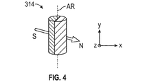
方法300は、図3Aに示すように、光学フィルム302中に所望の構造304を有する複数の磁化可能な粒子306を提供するように実施可能である。図3Bは、別の視点からの所望の構造304を示す図3Aの断面図を示す。複数の磁化可能な粒子306は、前に図示した又は記載したものと同様の構造を有することができる。一実施形態によると、ここで図3を参照すると、磁化可能な粒子は、(関心の対象である電磁スペクトルの範囲において)光学的に透明な樹脂中に分散されて、第1の混合物308を形成することができる。光学的に透明な樹脂は、図2を参照して提供される実施例と同じ組成を有することができる。第1の混合物308を、(基材312を含む)ウェブ310上に配置することができる。複数の磁化可能な粒子306は、樹脂の重量パーセントに対して、0.01%〜90%重量パーセントのいずれかであり得る。基材312の特定の化学組成及び厚さは、構築されている特定の光学製品の必要条件に依存し得る。すなわち、とりわけ、強度、透明度、耐熱性、表面エネルギー、光学層への接着、についての必要性のバランスをとることである。基材312の厚さは、典型的には、少なくとも約0.025ミリメートル(mm)、より典型的には少なくとも約0.125mmである。更に、基材312は一般に、約0.5mm以下の厚さを有する。
有用な基材材料としては、例えばスチレン−アクリロニトリル、酢酸酪酸セルロース、酢酸プロピオン酸セルロース、三酢酸セルロース、ポリエーテルスルホン、ポリメチルメタクリレート、ポリウレタン、ポリエステル、ポリカーボネート、ポリ塩化ビニル、ポリスチレン、ポリエチレンナフタレート、ナフタレンジカルボン酸に基づくコポリマー又はブレンド、ポリオレフィン系材料、例えばポリエチレン、ポリプロピレン、及びポリシクロ−オレフィンの、キャストフィルム又は配向フィルム、ポリイミド、及びガラスが挙げられる。任意選択的に、基材材料は、これらの材料の混合物又は組み合わせを含んでもよい。いくつかの実施形態では、基材は多層であってもよく、又は連続相中に懸濁若しくは分散された分散成分を含有してもよい。 Useful substrate materials include, for example, styrene-acrylonitrile, cellulose acetate butyrate, cellulose acetate propionate, cellulose triacetate, polyether sulfone, polymethylmethacrylate, polyurethane, polyester, polycarbonate, polyvinyl chloride, polystyrene, polyethylene naphthalate, etc. Comixes or blends based on naphthalenedicarboxylic acids, polyolefin-based materials such as polyethylene, polypropylene, and polycyclo-olefins, cast or oriented films, polyimides, and glasses. Optionally, the substrate material may include a mixture or combination of these materials. In some embodiments, the substrate may be multi-layered or may contain dispersed components suspended or dispersed in a continuous phase.
基材の更なる例としては、ポリエチレンテレフタレート(PET)及びポリカーボネートが挙げられる。有用なPETフィルムの例としては、DuPont Films(Wilmington,Del.)から、商品名「Melinex 618」で入手可能なフォトグレードポリエチレンテレフタレートが挙げられる。
Further examples of the substrate include polyethylene terephthalate (PET) and polycarbonate. Examples of useful PET films include photograde polyethylene terephthalate available from DuPont Films (Wilmington, Del.) Under the trade name "
任意選択的に、第2の基材(組成及び厚さにおいて第1の基材312と同様であっても同様でなくてもよい)を、光学フィルム302にラミネートして(laminate)(例えば、光学的に透明な接着剤を使用して接着させ)、透明度を向上させること、光学層304を保護すること、光学フィルム302に所望の物理的性質を提供すること、などができる。
Optionally, a second substrate (which may or may not be similar in composition and thickness to the first substrate 312) is laminated to the optical film 302 (eg, for example. It can be adhered using an optically transparent adhesive) to improve transparency, protect the
第1の混合物308は、磁石314(永久又は電磁石)のアップウェブに適用することができる。磁石314は、複数の磁化可能な粒子306と樹脂との第1の混合物308を含有するウェブ310の極めて近傍に(数フィート以内)置くことができる。磁石314に対するウェブ310の配置を理解すること、及び図3Aの所望の構造304を理解することに役立つように、デカルト座標系が図3及び図3Bに提供される。示される実施形態によれば、提供されるデカルト座標系は、ダウンウェブ/アップウェブ方向に配向された軸(x軸)を有することができる。(y軸)は、ウェブ310のクロスウェブ方向、及び磁石314の回転軸ARと実質的に整列している。(z軸)は、x軸及びy軸の両方に対して実質的に垂直に整列している。
The
図3の例に示すように、磁石314は、回転軸ARの周りに、ウェブ310に対して回転される。磁石の回転速度は、100〜10,000rpm、又はそれ以上であり得る。ウェブ310は、矢印316によって示すように磁石314に対して並進移動することができる。図4及び図4Aは、磁石314の構造を更に詳細に示す。図4は、磁石314が、それぞれ半球として成形され、回転軸ARの両側に配置された2つの極、N及びS、を含むことができることを示す。図4Aは、磁石314によって生成される磁界318、及び回転軸AR(図3及び図4)の周りの磁石314の回転により生じる磁界318の回転変調を示す。図3の方法300の光学フィルム302及び他の詳細は、図4Aには示されていない。複数の磁化可能な粒子306に及ぼされるであろう分解された磁力線は、図4Aの矢印Aによって示される。
As shown in the example of FIG. 3, the
磁界構成及び磁界を生成するための装置の更なる例は、米国特許出願公開第2008/0289262A1号(Gao)、及び米国特許第2,370,636号(Carlton)、同第2,857,879号(Johnson)、同第3,625,666号(James)、同第4,008,055号(Phaal)、同第5,181,939号(Neff)、及び英国特許第1477767号(Edenville Engineering Works Limited)に記載されており、これらはそれぞれ、参照によりその全体が本明細書に組み込まれる。 Further examples of magnetic field configurations and devices for generating magnetic fields are U.S. Patent Application Publication No. 2008/0289262A1 (Gao) and U.S. Pat. Nos. 2,370,636 (Carlton), 2,857,879. Johnson, 3,625,666 (James), 4,008,055 (Phaal), 5,181,939 (Neff), and U.S. Pat. No. 1,477,767 (Edenville Engineering). Works Limited), each of which is incorporated herein by reference in its entirety.
ここで図3に戻ると、例示的実施形態によれば、磁石314は、提供されるデカルト座標系のy軸方向にウェブ310のクロスウェブ延長の全体を横切って延びるように配置される。しかしながら、いくつかの実施形態では、磁石314は、図3に示すように、クロスウェブ長さ全体にわたって延びていなくてもよい。図3は、加えて、方法300が、図3において硬化1として示される少なくとも1つの硬化を光学フィルム302に適用することを示す。硬化1は、磁石314の近傍(アップウェブ又はダウンウェブに数インチ以内)に適用される。硬化1は、限定するわけではないが、例えば、紫外線光の適用、電子ビームの適用、熱エネルギーの適用又は除去(例えば、加熱又は冷却の適用)などの任意の既知の技術によって適用することができる。図4Aに示すように、磁界318が回転変調を受けている際に、複数の磁化可能な粒子が所望の構造304(図3A)になるように、磁力線と分解された磁力線とが所望の形態で配向される特定の時間及び場所において、硬化1の適用が光学フィルム302に適用されるべきである。硬化1は、完全な硬化(すなわち、樹脂の完全な重合が起こり得る)であることができる、又は磁化可能な粒子の大部分が所望の構造304(図3A)にあるような十分な重合を伴う部分硬化であることができる。完全硬化の場合は、図3の方法では、(硬化2として示される)第2の硬化は必要ないであろう。図3は、完全な重合を完了するために、ダウンウェブの場所での部分硬化(硬化1)及び第2の硬化(硬化2)を有する方法300を示す。
Returning to FIG. 3, according to an exemplary embodiment, the
したがって、図3の方法300は、第1の混合物308を基材310上に配置することを含めて、光を制御するための光学フィルムを作製することができる。第1の混合物308は、第1の樹脂中に分散された複数の磁化可能な粒子306を含むことができる。方法300は、複数の磁化可能な粒子306に対する少なくとも磁界318を回転変調することによって、複数の磁化可能な粒子306を、光を制御するための所望の構造304に組み立てることを含み得る。方法300は、複数の磁化可能な粒子306が所望の構造304にある間に、第1の樹脂の粘度を増加させるためにガラス化させる(例えば、上記の硬化1及び/又は硬化2による)ことを更に含み得る。
Therefore, the
図3Aは、高レベルで及び高度に概略的な形態で所望の構造304を示す。図3Aに示すように、基材312(図3)を除去することができる。しかしながら、他の実施形態では、基材312を保持することができる。前述したように、複数の磁化可能な粒子のうちの個々の粒子は、図3Aには示されていない。図3Aは、図2の光学フィルム200と同様の所望の構造304を有する光学フィルム302の構成を示す。所望の構造304は、複数の磁化可能な粒子が、概ねダウンウェブ方向に延びる離れた列320で構成されている構造である。所望の構造304は、図3Aに示す配向(x−z平面に平行)で直接見た場合に、光学フィルム302が実質的に光透過性になることを可能にする構造である。しかしながら、所望の構造304はまた、y−z平面(すなわち、図3Aの図に直交する、xz平面内ではない平面)内の光学フィルム302に対して傾斜した角度での光透過を制限する。図3及び図3Aの実施形態は、第1の混合物308を単一層として基材上に適用することについて記載されていることに留意することが重要である。しかしながら、同じ混合物又は異なる混合物の組成物を使用した複数の層の適用も考えられ、実際に、本開示において更に説明及び例示される。
FIG. 3A shows the desired
図5A〜図5Cは、本明細書に記載される複数の磁化可能な粒子のうちの例示的な粒子の更なる可能な配向、位置、及び整列を示す。図5Aは、粒子402及び404の特定の配向を示し、副表面がデカルト座標系のz方向及びx方向に構成され(図3〜図4Aで使用されているものと同じ配向系)、主表面がy方向に配向されている。そのような配向は、本質的に純粋に例示的であり、参照及び説明を容易にするために使用される。図5Aの多層配向では、粒子402及び404は、互いに積層され離されている。いくつかの実施形態では、粒子402及び404は、矢印Aによって示すように、互いに引き寄せられるか、又は反発するように構成され得る。
5A-5C show further possible orientations, positions, and alignments of exemplary particles among the plurality of magnetizable particles described herein. FIG. 5A shows the specific orientations of the
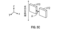
図5Bは、クロスウェブ方向に互いに離されている粒子406及び408を示す。いくつかの実施形態では、粒子406及び408は、矢印Aによって示すように、互いに引き寄せられるか、又は反発するように構成され得る。図5Cは、クロスウェブ方向に互いに離されている粒子410及び412を示す。いくつかの実施形態では、粒子410及び412は、矢印Aによって示すように、互いに引き寄せられるか、又は反発するように構成され得る。複数の粒子の複数の構成(例えば、図5A、図5B及び/又は図5Cが考えられ、実際に、本明細書にて開示されている。
FIG. 5B shows
図6は、複数の層を有する光学フィルム500の1つの可能な構成を示す。光学フィルム500は、前述したような基材502と、第1の層504とを有することができる。第1の層504は、第1の光学的に透明な樹脂508と第1の複数の磁化可能な粒子510との第1の混合物506を含むことができる。第1の層504は、直接的に又は間接的に、基材502に結合することができる。図6では、第1の複数の磁化可能な粒子510の相対的なサイズ及び間隔は、例示目的で及び見る人の理解のために誇張されている。図6に示すように、第1の複数の磁化可能な粒子510は、第1の所望の構造511を有する。
FIG. 6 shows one possible configuration of an
図6では、第2の層512は、直接的に又は間接的に(例えば、第2の基材を介して)第1の層506に結合することができる。第2の層512は、第2の光学的に透明な樹脂516と第2の複数の磁化可能な粒子518との第2の混合物514を含むことができる。図6では、第2の複数の磁化可能な粒子518の相対的なサイズ及び間隔は、例示目的で及び見る人の理解のために誇張されている。図6に示すように、第2の複数の磁化可能な粒子518は、第2の所望の構造519を有する。第2の所望の構造518は、第1の所望の構造511とは異なるか、又は実質的に同様であり得る。
In FIG. 6, the
図6に示すように、第1の複数の磁化可能な粒子510は、基材502に対して共有された第1の配向又は第1の共通整列方向のうちの少なくとも一方を有することができ、第2の複数の粒子518は、基材502に対して共有された第2の配向又は第2の共通整列方向のうちの少なくとも一方を有することができる。図6では、共有された第1の配向又は第1の共通整列方向は、共有された第2の配向又は第2の共通整列方向とは異なる。
As shown in FIG. 6, the first plurality of
任意選択的に、更なる所望の構造を有する磁化可能な粒子を有する層を含む更なる層を光学フィルム500に追加することができる。図6の実施形態は、光学フィルムの基材502とは反対側に沿って、光学フィルム500に平滑な表面を提供するように構成され得る更なる層520を示す。他の場合には、更なる層520は、所望であれば、所望のテクスチャリング又は他の物理的属性を提供することができる。
Optionally, an additional layer can be added to the
図7は、光を制御するための少なくとも2つの層を有する光学フィルム602を形成する別の方法600を示す。本開示の残りの部分については特に更に指示がない限り、磁石、樹脂、磁化可能な粒子、基材の構造及び構成は、本明細書で前述したものと実質的に類似であるか又は同じであり得る。したがって、例えば、各磁石は、特に指示がない限り、図3〜図4Aの磁石314と同様の回転を受ける。したがって、このような磁石によって生成される磁界は、回転振動を受ける。
FIG. 7 shows another
方法600は、第1の混合物608を基材612上に配置すること(「混合物を適用」で示される)を含み得る。第1の混合物608は、第1の樹脂607(図7A及び図7B)中に分散された複数の磁化可能な粒子606(図7A及び図7Bを参照)を含み得る。方法600は、複数の磁化可能な粒子606に対する第1の磁界618を回転変調することによって、第1の複数の磁化可能な粒子606を、光を制御するための所望の構造604A及び604B(ここでも図7A及び図7Bを参照)に組み立てることを含み得る。方法300は、複数の磁化可能な粒子606が所望の構造604A又は604Bにある間に、第1の樹脂の粘度を増加させるためにガラス化すること(「硬化1」として示される)を更に含むことができる。
図7A及び図7Bは、方法600から得られ得る所望の構造604A及び604Bを示す。これらの所望の構造は、第1の磁石614及び第2の磁石620を、光学フィルム602に対してクロスウェブ及びダウンウェブの両方向に配向させることから生じる。第1の磁石614及び第2の磁石620のこの配向は、磁界618及び622を、第1の複数の磁化可能な粒子606及び第2の複数の磁化可能な粒子624に印加される際に変化させる。
7A and 7B show the desired
第1の磁石614の配向は、図7の軸AA1の周りの矢印A1によって示すように、光学フィルム602に対して変えることができる。同様に、第2の磁石620の配向は、軸AA2の周りの矢印A2によって示すように、光学フィルム602に対して変えることができる。第1の磁石614及び/又は第2の磁石620を互いに対して及び光学フィルムに対して所望に応じて配向させることによって、(第1の磁石614の配向/再配向によって)第1の所望の構造604A及び604Bを含む異なる全体的な所望の構造を得ることができる。図7A及び図7Bは、第2の磁石620の配向/再配向から生じる、第2の複数の磁化可能な粒子624に対する第2の所望の構造626A及び626Bを更に示す。第2の所望の構造626Aを第1の所望の構造604Aと組み合わせると、図7Aに示す全体的な所望の構造が提供される。第2の所望の構造626Bを第1の所望の構造604Bと組み合わせると、図7Bに示す全体的な所望の構造が提供される。繰り返すと、図7A及び図7Bの全体的な所望の構造は、第1の磁石614及び第2の磁石620の異なる配向に起因して異なり得る。
The orientation of the
図7A及び図7Bは、可能な所望の構造の2つの例のみを提供しており、具体的に示していないが、光学フィルムに対する第1の磁石及び第2の磁石の配向に起因して異なる形状を有する更なる所望の構造も考えられることに留意すべきである。図7A及び図7Bでは、第1の所望の構造604A又は604Bが、第2の所望の構造626A又は626Bと同じ層内にあるように見えるが、これは図7A及び図7Bを見る向きの結果であり、第1の所望の構造604A又は604Bは実際には、第2の所望の構造626A又は626Bとは異なる光学フィルム602の層内に配置されるであろうことにも更に留意すべきである。
7A and 7B provide only two examples of possible desired structures and are not specifically shown, but differ due to the orientation of the first and second magnets with respect to the optical film. It should be noted that additional desired structures with a shape are also conceivable. In FIGS. 7A and 7B, the first desired
所望の構造604A又は604Bにより、光学フィルム602をz軸に直接平行に見たときに実質的に光透過性であることが可能になる。しかしながら、所望の構造604A又は604Bはまた、光学フィルム602に対して傾斜した角度での光透過を制限する(構造が二次元なので、これはy−z平面に限定されない。
The desired
図7の方法600は、複数の層を有する光学フィルム602を形成するので、方法600は、第2の樹脂630中に分散された第2の複数の磁化可能な粒子624(図7A及び図7B)を含む第2の混合物628を形成すること(「混合物を適用」で示される)を含むことができる。方法600は、第2の混合物628を、基材、第2の基材、又は第1の混合物のうちの1つ以上の上に配置することができる。方法600は、第2の複数の磁化可能な粒子624に対する第2の磁界622を更に回転変調することによって、第2の複数の磁化可能な粒子624を、光を制御するための第2の所望の構造626A又は626Bに組み立てることができる。この方法は、第2の複数の磁化可能な粒子624が第2の所望の構造626A又は626Bにおける列である間に、第2の樹脂630(硬化2として示される)の粘度を増加させることができる。
Since the
いくつかの実施形態では、第2の混合物628及び第1の混合物608は、異なる組成物を有する、又は実質的に同じ組成物を有する、のいずれか一方である。第1の混合物608及び第2の混合物628の組成が実質的に同じ組成である場合、第1の複数の磁化可能な粒子が第1の所望の構造604A又は604Bにある間、かつ第1の樹脂608の粘度を増加させた後に、図8の方法700に従って第2の混合物628を配置することができる。
In some embodiments, the
図8は、光を制御するための少なくとも2つの層を有する光学フィルム602を形成する更なる方法700を示す。方法700は、第2の樹脂630(図7A及び図7B)が第1の樹脂607(図7A及び図7B)と共に硬化されないように、硬化1の後に第2の混合物628が(「層を追加」と)表示された箇所においてウェブに適用され得るという点で、図7の方法600とは異なる。
FIG. 8 shows a
図9、図9A、及び図9Bは、硬化1の前に、又は硬化1の前そして次に再び硬化2の前に適用することができる複数の層を有する光学フィルム802を形成する方法800を示す。方法800は、光学フィルム802に対する磁石804の配向に起因して、前述したように、例えば、第1の所望の構造604A又は604B及び第2の所望の構造626A又は626Bを提供することができる。図9、図9A、及び図9Bの方法800は、単一の磁石804を利用できるという点で図7〜図8とは異なる。硬化1における磁石の回転軸とウェブとの間の距離は、硬化2における回転軸とウェブとの間の距離とは異なっていてもよい。単一の磁石804は、図9及び図9Aの視野Aによって示すように、硬化1の領域内の光学フィルム802上に回転変調することを伴う第1の印加磁界808を発生させ、図9Bの視野Bによって示すように、硬化2の領域内に回転変調すること(少なくとも配向に起因して、第1の印加磁界808とは異なる)を伴う第2の印加磁界810を生成する。このようにして、方法800は、単一の磁石を使用して、光学フィルム802の複数の層内に図9Cのような所望の構造812及び814を生成することができる。
9, 9A, and 9B show a
図10は、軸AA3の周りで往復する矢印O1及びO2によって示すように揺動する形態で磁石904を移動させることができることを除いて、方法300と同じであり得る光学フィルム902を形成する方法900を示す。この揺動運動は、前述したような回転軸ARの周りの磁石904の回転に追加されるものである。したがって、磁石904によって生成される磁界906は、光学フィルム902に対して回転変調することと揺動の両方を有することになる。
FIG. 10 shows a method of forming an
図10Aは、磁界906の適用から生じる、光学フィルム902内の複数の磁化可能な粒子910の所望の構造908を示す。所望の構造908は、磁界906の揺動運動に起因して、ダウンウェブ方向に正弦波パターンを有する。
FIG. 10A shows the desired structure 908 of the plurality of
図10Bは、別の実施形態に係る、光学フィルム902内の複数の磁化可能な粒子910のついての別の所望の構造912を示し、図10に示すように360度未満の円弧状に往復して揺動するよりもむしろ、磁石904を、軸AA3の周りに360度連続して完全に回転させて、図10Bに示す構造のような繰り返しリングを生成する。
FIG. 10B shows another desired
図11は、この方法が、複数の磁石1004及び1006を利用し、光学フィルム1002が複数の層を有することは除いては、図10の方法900と同一である光学フィルム1002を形成する方法1000を示す。図11Aは、2つの層について所望の構造1008及び1010を有する光学フィルム1002を示す。所望の構造1008は、第1の複数の磁化可能な粒子1012を有する。所望の構造1010は、第2の複数の磁化可能な粒子1014を有する。第1の複数の磁化可能な粒子1012は、第2の複数の磁化可能な粒子1014とは異なる配向を有する。
FIG. 11 shows a
図12は、光学フィルム1102を形成する方法1100を示し、少なくとも部分硬化の場所を、磁石1106によりアップウェブ又はダウンウェブにシフトさせることができる。硬化におけるこのシフトは、磁石1106の回転に起因する回転変調を受ける、磁界1104からの磁力線が、光学フィルム1102の主表面1108に対して異なる角度にある場所へのシフトであり得る。図12の実施形態では、磁石1106は、以前に示し説明した磁石に対して再配向されていることに留意されたい。磁石1106は、概ねアップウェブ方向及びダウンウェブ方向に延び、デカルト座標系(この座標系は、図全体にわたって維持されている)のx方向と整列する回転軸ARを有する。光学フィルム1102が受ける磁力線の角度は、主表面1108に対して実質的に直交する角度から測定されるように示され、0度の角度は主表面に実質的に直交し、25度の角度は直交から実質的に25度であり、45度の角度は直交から実質的に45度である、といった具合である。
FIG. 12 shows a
図12Aは、図12の方法1100を示すが、図12の視野に直交する角度におけるものである。図12Aは、光学フィルム1102を、ローラー、気流、テンティング(tenting)、ウェブ張力、又は別の技術によって、クロスウェブ方向に湾曲させるか又は別の方法で成形し得ることを更に示す。光学フィルム1102をクロスウェブ方向にこのように成形することにより、光学フィルム1102の主表面1108が、磁石1106の曲率に概ね対応し一致する曲率を有するようにできる。光学フィルム1102をこのように成形することにより、主表面1108にとって、矢印Aで示すようなクロスウェブ方向の磁界1104の磁力線に対する相対角度が実質的に同じになることが可能になる。換言すれば、磁石1106の外面の曲率と実質的に一致する光学フィルム1102の曲率ゆえに、矢印Aの各々が、主表面1108に対して実質的に同じ角度を有する。したがって、複数の磁化可能な粒子は、異なるクロスウェブの場所に位置する場合であっても、磁界1104に対して実質的に同じ相対角度になる。
12A shows the
図13は、図12で前述した方法1100を利用する例を示し、ダウンウェブ方向における硬化の場所が磁石1106に対して変更され、それにより、磁石1106の回転に起因する回転変調を受ける磁界1104からの磁力線は、主表面1108に直交する方向から測定して実質的に0度、及び主表面1108に直交する方向から測定して実質的に25度の角度にある。
FIG. 13 shows an example of utilizing the
図13Aは、図13の方法から、光学フィルム1102に対してもたらされた所望の構造1110を示す。図13Bは、図13Aの線13B−13Bに沿った断面における所望の構造1110を示す。
FIG. 13A shows the desired structure 1110 brought to the
図14は、磁界1205を有する磁石1204に対して、光学フィルム1202の相対位置を(矢印Aで示すように)変えた方法1200を示す。より具体的には、光学フィルム1202の主表面1214と磁石1204の回転軸ARとの間の距離が変化するように、磁石1204及び磁界1205から、相対的に近い位置1206と相対的に離れた位置1208との間で、光学フィルム1202を移動させることができる。光学フィルム1202が相対的に近い位置1206にある場合は、複数の磁化可能な粒子の軌道は、より近く離れる傾向があり、光学フィルム1202が相対的に離れた位置1208にある場合は、複数の磁化可能な粒子の軌道は、より広く離れる傾向がある。図14及び図15(後で論じられる)では、磁石1204、1304は、以前に図3に示したように実質的にクロスウェブに配向され、したがって、図12〜図13のようには配向されないことに留意されたい。しかしながら、他の実施形態では、磁石1204、1304は、図12〜図13に示すように光学フィルム1202、1302に対して配向され得ることに留意すべきであり、方法1200、1300は、図14A、図14B、及び図15Aに示すものとは異なる所望の構造を得るために利用される。
FIG. 14 shows a
図14A及び図14Bは、複数の磁化可能な粒子1212に対する所望の構造1210を示す。図14C〜図14Eは、図14A及び図14Bの様々な断面からの所望の構造1210を示す。図14Aは、図14の方法及び図3の方法を組み合わせることによって形成されるダウンウェブ方向(x方向)への複数の磁化可能な粒子1212の波形トラックであり、図3の方法はダウンウェブトラックを形成する傾向があり、図14の方法は、これらのトラックの間隔を変化させる傾向がある。図14Bは、図14の方法と図12の方法とを組み合わせることによって形成され、図12の方法はクロスウェブトラックを形成する傾向があり、図14の方法は、これらのトラックの間隔を変化させる傾向がある。
14A and 14B show the desired
図15は、磁界1305を有する磁石1304に対して、光学フィルム1302の第1の部分1303のみの相対位置を(矢印Aで示すように)変えた方法1300を示す。より具体的には、光学フィルム1302の第1の部分1303は、磁石1304及び磁界1305から、相対的に近い位置1306と相対的に離れた位置1308との間で移動する(例えば、傾ける)ことができる。光学フィルム1302の第2の端部1307は、磁石1304及び磁界1305に対して、実質的に同じ位置に、又はわずかに変更された位置に留まることができる。
FIG. 15 shows a
図15Aは、光学フィルム1302の第1の部分1303の、1306の位置及び1308の位置からの位置の往復変化から生じる、所望の構造1310を示す。図15B及び図15Cは、図15Aからの所望の構造1310の断面図である。図15Aに示すように、位置1308への変化及び位置1306へと戻る変化により、複数の磁化可能な粒子がクロスウェブ方向に傾いた領域1312がもたらされる。
FIG. 15A shows the desired
図16は、方法900〜1300の様々な方法を組み合わせて多層光学フィルム1402、1404、及び1406を形成する実施例を示す。実際に、本明細書に開示される方法のいずれも、組み合わせるか又は修正して、例えば、光を制御するための様々な所望の構造で組織化された複数の磁化可能な粒子を有する多層光学フィルムを形成することができることに留意すべきである。
FIG. 16 shows an example in which various methods of
図17は、光学フィルム1502を作製するための、別の実施形態による方法1500であり、光学フィルムは、図17Aに示すように、全体的な所望の構造1506に組織化された第1の複数の磁化可能な粒子1504及び第2の複数の磁化可能な粒子1505を有する。方法1500は、少なくとも2つの磁石1508及び1510を利用することができる。第1の磁石1508は、回転軸ARの周りに回転することができ、回転変調することを伴う第1の磁界1512を有することができる。第2の磁石1510は、回転軸ARの周りに回転することができ、回転変調することを伴う第2の磁界1514を有することができる。加えて、第1の磁石1508は、矢印T1及びT2によって示すように、クロスウェブ(y軸)方向に往復で並進移動することができる。
FIG. 17 is a
図17Aは、方法1500から得られた、多層光学フィルム1502についての全体的な所望の構造1506を示し、第1の複数の磁化可能な粒子1504が第1の磁界1512によって配置、配向、及び/又は整列されて第1の所望の構造体1516になり、第2の複数の磁化可能な粒子1505が第2の磁界1514によって配置、配向、及び/又は整列されて第2の所望の構造体1518になっている。図17Aに示すように、第1の所望の構造1516の第1の複数の磁化可能な粒子1504の列が、第2の所望の構造1518の第2の複数の磁化可能な粒子1505の列を横断して配向されている。
FIG. 17A shows the overall desired
図18は、フィーチャ1604及び/又は1606を、光学的に透明な樹脂及び複数の磁化可能な粒子を含有する少なくとも第1の混合物の少なくとも部分硬化の前に、最中に、又は後に、光学フィルム1602に付与することができる方法1600を示す。図18は、第1の磁石1608に隣接する第1の部分硬化(「硬化1」)を実行し、第1の磁石1608からダウンウェブに第2の完全硬化(「硬化2」)適用する方法1600を示す。フィーチャは、光学フィルム1602に付与することができ、又は、方法1600の適用前に、光学フィルム1602の初期的なウェブに固有に存在するように事前に作製することができる。フィーチャは、限定するものではないが、光学フィルム1602をクロスウェブ方向に一時的に湾曲させること(図12及び図12Aに前述)、光学フィルム1602をアップウェブ/ダウンウェブ方向に湾曲させる/歪ませること、光学フィルムに磁化可能な粒子、基材、及び/又は層を更に付与すること(前述)、基材にテクスチャを追加すること(図19に示す)、複数の磁化可能な粒子を含有する層にテクスチャを追加すること(図20に示す)、プロファイルダイ(profiled die)又は別のツールを用いて混合物/層に厚さ変動を付与すること、複数の磁化可能な粒子を含有する不連続層を設けること、磁界に局所的不規則性を提供すること、磁界に磁束集中を提供すること、磁石によって印加される磁界強度(磁力)を増加又は減少させること、及び/又は可変厚さを有する基材を提供すること、を含む。
FIG. 18 shows an optical film with
図19は、少なくとも部分硬化(図18の「硬化1」)の前に、最中に、又は後に、装置1610によってフィーチャが基材に付与される方法1600を示す。これらのフィーチャは、磁石の回転軸に対する基材の、基材の位置及び角度が、1つの領域(領域1612)と別の領域とで変化し得るように、クロスウェブ、ダウンウェブ、又はその両方のいずれかの方向における基材のテクスチャ加工を含み得る。この基材のテクスチャ加工により、ある領域における複数の磁化可能な粒子が、他の領域におけるものとは異なる配置、配向、又は整列を有し得るように、複数の磁化可能な粒子を含有する層1614を変化させることができる。図20は、フィーチャが基材によってではなく装置1610によって層1614に直接付与される方法1600を示す。層1614をテクスチャ加工することにより、ある領域における複数の磁化可能な粒子が、他の領域におけるものとは異なる配置、配向、又は整列を有し得るように、複数の磁化可能な粒子を含有する層1614の厚さを、クロスウェブ、ダウンウェブ、又はその両方のいずれかの方向で変化させることができる。
FIG. 19
図21は、その磁界1704中に局所的不規則性を形成するための複合アセンブリである磁石1702を示す。より具体的には、磁石1702は、第1の磁界1708を有する第1の部分1706と、第2の磁界1712を有する第2の部分1710とを有する。第1の部分1702は、第1の部分1706の極Nが第2の部分1710の極Nと直接整列しないように、軸Aの周りにわずかに回転されている。したがって、第1の磁界1708は、第2の磁界1712とは配向が異なっており、そのような配向のシフトは、本開示において局所的不規則性と呼ばれる。
FIG. 21 shows a
図22は、磁石1802の表面に沿った突出部1808に起因する磁束集中1806を有する磁界1804を有する磁石1802を示す。このような突出部は、磁石1802の一部とすることができ、又は磁石1802とは別個の鉄片であってもよい。磁束集中に関する更なる情報は、PCT国際公開第2018/136269号に見出すことができ、その開示全体が参照により本明細書に組み込まれる。
FIG. 22 shows a
図23及び図23Aは、可変厚さを有するように製作された基材1904を有する光学フィルム1902を示す。基材1904は、交互の山部1906及び谷部1908を有することができる。谷部1908は、図23Aに示すように、複数の磁化可能な粒子1910を内部に収容するように構成され得る。光学的に透明な樹脂は、図23Aには示されていない。山部1908は、複数の磁化可能な粒子1910を図23Aに示す配向にガイドすることによって、かつ複数の磁化可能な粒子1910をその側面に沿って支持することによって、複数の磁化可能な粒子1910が所望の配向を実現することを支援するように構成され得る。谷部1908は、複数の磁化可能な粒子1910が、所望の配向で、並びに図23Aに示すような相対間隔で配置されることを支援するように構成され得る。
23 and 23A show an
以下の実施形態は、本開示を例示することが意図され、限定するものではない。 The following embodiments are intended to illustrate, but are not limited to, the present disclosure.
様々な注記及び実施例
実施例1は、光を制御するための光学フィルムを作製する方法であって、第1の混合物を基材上に配置することであって、第1の混合物は、第1の樹脂中に分散された第1の複数の磁化可能な粒子を含む、配置することと、第1の複数の磁化可能な粒子に対する少なくとも第1の磁界を回転変調することによって、第1の複数の磁化可能な粒子を、光を制御するための所望の構造に組み立てることと、第1の複数の磁化可能な粒子が所望の構造にある間に第1の樹脂をガラス化することと、を任意選択的に含み得る方法である。
Various Notes and Examples Example 1 is a method of making an optical film for controlling light, in which the first mixture is placed on a substrate, and the first mixture is the first. A first by arranging, including a first plurality of magnetizable particles dispersed in one resin, and by rotationally modulating at least a first magnetic field with respect to the first plurality of magnetizable particles. Assembling the plurality of magnetizable particles into a desired structure for controlling light, and vitrifying the first resin while the first plurality of magnetizable particles are in the desired structure. Is a method that can optionally include.
実施例2は、第1の樹脂をガラス化することが、第1の樹脂を少なくとも部分的に重合させることを含み得る、実施例1に記載の方法である。 Example 2 is the method of Example 1, wherein vitrification of the first resin may include at least partially polymerizing the first resin.
実施例3は、第2の樹脂中に分散された第2の複数の磁化可能な粒子を含む第2の混合物を形成することと、第2の混合物を、基材、第2の基材、又は第1の混合物のうちの1つ以上の上に配置することと、更に第2の複数の磁化可能な粒子に対する少なくとも第2の磁界を回転変調することによって、第2の複数の磁化可能な粒子を、光を制御するための第2の所望の構造に組み立てることと、第2の複数の磁化可能な粒子が第2の所望の構造にある間に第2の樹脂をガラス化することと、を任意選択的に更に含む、実施例1又は2に記載の方法、又は実施例1及び2を組み合わせた方法である。 In Example 3, a second mixture containing a second plurality of magnetizable particles dispersed in the second resin is formed, and the second mixture is used as a base material, a second base material, and the like. Alternatively, a second plurality of magnetizable particles can be generated by placing them on one or more of the first mixture and by rotationally modulating at least a second magnetic field with respect to the second plurality of magnetizable particles. Assembling the particles into a second desired structure for controlling light and vitrifying the second resin while the second plurality of magnetizable particles are in the second desired structure. , Is optionally further included, the method according to Example 1 or 2, or a method in which Examples 1 and 2 are combined.
実施例4は、第2の混合物及び第1の混合物が、異なる組成を有する、又は実質的に同じ組成を有する、のいずれか一方であることができ、実質的に同じ組成を有する場合、第1の複数の磁化可能な粒子が所望の構造にある間、かつ第1の樹脂の粘度を増加させた後に、第2の混合物が配置され得る、実施例3に記載の方法である。 In Example 4, when the second mixture and the first mixture can either have different compositions or have substantially the same composition, and have substantially the same composition, the first The method of Example 3, wherein the second mixture can be placed while the plurality of magnetizable particles of 1 are in the desired structure and after increasing the viscosity of the first resin.
実施例5は、第1の複数の磁化可能な粒子が、基材に対して共有された第1の配向又は第1の共通整列方向のうちの少なくとも一方を有することができ、第2の複数の粒子が、基材に対して共有された第2の配向又は第2の共通整列方向のうちの少なくとも一方を有することができ、共有された第1の配向又は第1の共通整列方向が、共有された第2の配向又は第2の共通整列方向とは異なり得る、実施例3又は4に記載の方法、又は実施例3及び4を組み合わせた方法である。 In Example 5, the first plurality of magnetizable particles can have at least one of the first orientation or the first common alignment direction shared with respect to the substrate, and the second plurality. Particles can have at least one of a shared second orientation or second common alignment direction with respect to the substrate, and the shared first orientation or first common alignment direction is The method according to Example 3 or 4, or a method in which Examples 3 and 4 are combined, which may be different from the shared second orientation or the second common alignment direction.
実施例6は、第1の複数の磁化可能な粒子に対する少なくとも第1の磁界を回転変調することと、第2の複数の磁化可能な粒子に対する少なくとも第2の磁界を回転変調することとが、単一の磁石からのものである、実施例3〜5のいずれか1つに記載の方法、又は実施例3〜5に記載の方法を任意に組み合わせた方法である。 In the sixth embodiment, at least the first magnetic field for the first plurality of magnetizable particles is rotationally modulated, and at least the second magnetic field for the second plurality of magnetizable particles is rotationally modulated. The method according to any one of Examples 3 to 5, which is from a single magnet, or a method in which the methods according to Examples 3 to 5 are arbitrarily combined.
実施例7は、第1の複数の磁化可能な粒子を第1の磁界に対して1つ以上の方向に移動させることと、第1の磁界を第1の複数の磁化可能な粒子に対して少なくとも第2の方向に移動させることと、第1の磁界の強度を変化させることと、第1の磁界において局所的不規則性又は磁束集中のうちの少なくとも1つを提供することと、のうちの1つ以上によって、第1の磁界を第1の複数の磁化可能な粒子に対して変化させることを、任意選択的に更に含み得る、実施例1〜6のいずれか1つに記載の方法、又は実施例1〜6に記載の方法を任意に組み合わせた方法である。 In the seventh embodiment, the first plurality of magnetizable particles are moved in one or more directions with respect to the first magnetic field, and the first magnetic field is transferred to the first plurality of magnetizable particles. Of moving at least in the second direction, changing the strength of the first magnetic field, and providing at least one of local irregularities or flux concentration in the first magnetic field. The method according to any one of Examples 1 to 6, which may optionally further include altering the first magnetic field with respect to the first plurality of magnetizable particles by one or more of the above. , Or a method in which the methods described in Examples 1 to 6 are arbitrarily combined.
実施例8は、第1の複数の磁化可能な粒子を第1の磁界に対して移動させることが、第1の混合物及び基材のうちの1つ以上にテクスチャを適用して第1の混合物及び基材のうちの1つ以上に可変厚さを提供することと、基材及び第1の混合物をダウンウェブ方向及びクロスウェブ方向のうちの1つ以上に湾曲させることと、基材及び第1の混合物を歪ませることと、基材が可変厚さを有しかつ第1の混合物を基材上に堆積させることと、のうちの1つ以上を含み得る、実施例7に記載の方法である。 In Example 8, moving a first plurality of magnetizable particles with respect to a first magnetic field applies a texture to one or more of the first mixture and the substrate to make the first mixture. And to provide variable thickness to one or more of the substrates, to bend the substrate and the first mixture to one or more of the downweb and crossweb directions, and to provide the substrate and the first mixture. The method of Example 7, wherein the mixture of 1 may be distorted, the substrate may have a variable thickness and the first mixture may be deposited on the substrate, and one or more of the following may be included. Is.
実施例9は、第1の磁界を第1の複数の磁化可能な粒子に対して少なくとも第2の方向に移動させることが、第1の磁界を、第1の磁界の回転軸に直交する平面内でクロスウェブ及びダウンウェブのうちの1つ以上の方向に並進移動させることと、第1の磁界を、第1の磁界の回転軸に直交する平面内でクロスウェブ及びダウンウェブのうちの1つ以上の方向に揺動させることと、のうちの1つ以上を含み得る、実施例7又は8に記載の方法、又は実施例7及び8に記載の方法を任意に組み合わせた方法である。 In Example 9, moving the first magnetic field in at least a second direction with respect to the first plurality of magnetizable particles causes the first magnetic field to be a plane orthogonal to the axis of rotation of the first magnetic field. Translational movement in one or more directions of the crossweb and downweb within, and one of the crossweb and downweb in a plane orthogonal to the axis of rotation of the first magnetic field. A method according to Example 7 or 8, or a method in which the methods according to Examples 7 and 8 are arbitrarily combined, which may include swinging in one or more directions and one or more of them.
実施例10は、光を制御するための光学フィルムを作製する方法であって、基材と、第1の樹脂中に分散された第1の複数の磁化可能な粒子を含む第1の混合物と、第2の樹脂中に分散された第2の複数の磁化可能な粒子を含む第2の混合物と、を提供することと、第1の複数の磁化可能な粒子に対する少なくとも第1の磁界を回転変調することによって、第1の複数の磁化可能な粒子を、光を制御するための第1の所望の構造に組み立てることと、第1の所望の構造に組み立てられた第1の複数の磁化可能な粒子を有する第1の樹脂をガラス化することと、第2の複数の磁化可能な粒子に対する少なくとも第2の磁界を回転変調することによって、第2の複数の磁化可能な粒子を、光を制御するための第2の所望の構造に組み立てることと、第2の所望の構造に組み立てられた第2の複数の磁化可能な粒子を有する第2の樹脂をガラス化することと、を任意選択的に含み得る方法である。 Example 10 is a method of making an optical film for controlling light, which comprises a substrate and a first mixture containing a first plurality of magnetizable particles dispersed in a first resin. To provide a second mixture containing a second plurality of magnetizable particles dispersed in a second resin, and to rotate at least a first magnetic field with respect to the first plurality of magnetizable particles. By modulating, the first plurality of magnetizable particles are assembled into a first desired structure for controlling light, and a first plurality of magnetizable particles assembled into the first desired structure. By vitrifying the first resin having the same particles and rotationally modulating at least the second magnetic field with respect to the second plurality of magnetizable particles, the second plurality of magnetizable particles are exposed to light. Optional choice between assembling into a second desired structure for control and vitrifying a second resin having a second plurality of magnetizable particles assembled into the second desired structure. It is a method that can be included in the target.
実施例11は、第1の樹脂及び第2の樹脂が異なる組成を有することができ、異なるガラス化技術を使用してガラス化され得る、実施例10に記載の方法である。 Example 11 is the method of Example 10, wherein the first resin and the second resin can have different compositions and can be vitrified using different vitrification techniques.
実施例12は、異なるガラス化技術は、UVガラス化を含み、第1の樹脂を第1の波長でガラス化し第2の樹脂を第2の波長でガラス化するものである、実施例11に記載の方法である。 In Example 12, different vitrification techniques include UV vitrification, in which the first resin is vitrified at the first wavelength and the second resin is vitrified at the second wavelength. This is the method described.
実施例13は、第1の複数の磁化可能な粒子を第1の磁界に対して1つ以上の方向に移動させることと、第1の磁界を第1の複数の磁化可能な粒子に対して少なくとも第2の方向に移動させることと、第1の磁界の強度を変化させることと、第1の磁界において局所的不規則性又は磁束集中のうちの少なくとも1つを提供することと、のうちの1つ以上によって、少なくとも第1の磁界を第1の複数の磁化可能な粒子に対して変化させることを任意選択的に更に含む、実施例10〜12のいずれか1つに記載の方法、又は実施例10〜12に記載の方法を任意に組み合わせた方法である。 In the thirteenth embodiment, the first plurality of magnetizable particles are moved in one or more directions with respect to the first magnetic field, and the first magnetic field is transferred to the first plurality of magnetizable particles. Of moving at least in the second direction, changing the strength of the first magnetic field, and providing at least one of local irregularities or flux concentration in the first magnetic field. The method according to any one of Examples 10 to 12, further optionally further varying at least a first magnetic field with respect to the first plurality of magnetizable particles by one or more of the above. Alternatively, it is a method in which the methods described in Examples 10 to 12 are arbitrarily combined.
実施例14は、第1の複数の磁化可能な粒子を第1の磁界に対して移動させることが、第1の混合物及び基材のうちの1つ以上にテクスチャを適用して第1の混合物及び基材のうちの1つ以上に可変厚さを提供することと、基材及び第1の混合物をダウンウェブ方向及びクロスウェブ方向のうちの1つ以上に湾曲させることと、基材及び第1の混合物を歪ませることと、基材が可変厚さを有しかつ第1の混合物を基材上に堆積させることと、のうちの1つ以上を含み得る、実施例13に記載の方法である。 In Example 14, moving a first plurality of magnetizable particles with respect to a first magnetic field applies a texture to one or more of the first mixture and the substrate to make the first mixture. And to provide variable thickness to one or more of the substrates, to bend the substrate and the first mixture to one or more of the downweb and crossweb directions, and to provide the substrate and the first mixture. 13. The method of Example 13, wherein the mixture of 1 may be distorted, the substrate may have a variable thickness and the first mixture may be deposited on the substrate, and one or more of the following may be included. Is.
実施例15は、第1の磁界を第1の複数の磁化可能な粒子に対して少なくとも第2の方向に移動させることが、第1の磁界を、第1の磁界の回転軸に直交する平面内で、クロスウェブ及びダウンウェブのうちの1つ以上の方向に並進移動させることと、第1の磁界を、第1の磁界の回転軸に直交する平面内でクロスウェブ及びダウンウェブのうちの1つ以上の方向に揺動させることと、のうちの1つ以上を含み得る、実施例12又は13に記載の方法、又は実施例12及び13に記載の方法を任意に組み合わせた方法である。 In Example 15, moving the first magnetic field in at least a second direction with respect to the first plurality of magnetizable particles causes the first magnetic field to be a plane orthogonal to the axis of rotation of the first magnetic field. Within, translating in one or more of the cross-web and down-web directions, and moving the first magnetic field out of the cross-web and down-web in a plane orthogonal to the axis of rotation of the first magnetic field. A method according to Example 12 or 13, or a method in which the methods according to Examples 12 and 13 are arbitrarily combined, which may include swinging in one or more directions and one or more of them. ..
実施例16は、光を制御するための光学フィルムを作製する方法であって、第1の磁石を、第1の複数の磁化可能な粒子が第1の樹脂中に分散されている第1の混合物を少なくとも含有するウェブに対して配置することと、第1の磁石のN極及びS極がウェブの近傍を交互に通過するように、第1の磁石を軸の周りに回転させることと、第1の複数の磁化可能な粒子が、第1の磁石の磁界によって影響を受けて、第1の磁界によって影響を及ぼされた所望の構造を形成するように、ウェブを第1の磁石に隣接させて通過させることであって、所望の構造は光を制御するように構成されている、通過させることと、第1の樹脂をガラス化して第1の複数の磁化可能な粒子を所望の構造にて捕捉することと、を任意選択的に含み得る方法である。 Example 16 is a method of producing an optical film for controlling light, wherein a first magnet is provided with a first plurality of magnetizable particles dispersed in a first resin. Placing the mixture relative to the web containing at least, and rotating the first magnet around an axis so that the north and south poles of the first magnet pass alternately in the vicinity of the web. Adjacent the web to the first magnet so that the first plurality of magnetizable particles are affected by the magnetic field of the first magnet to form the desired structure affected by the first magnetic field. Passing through, the desired structure is configured to control light, passing and vitrifying the first resin to allow the first plurality of magnetizable particles to pass through the desired structure. It is a method that can optionally include capturing with.
実施例17は、第2の磁石をウェブに対して配置することであって、ウェブは、ウェブ上に堆積された、第2の複数の磁化可能な粒子が第2の樹脂中に分散されている第2の混合物を少なくとも有する、配置することと、第2の磁石のN極及びS極がウェブの近傍を交互に通過するように、第2の磁石を軸線の周りに回転させることと、第2の複数の磁化可能な粒子が、第2の磁石の磁界によって影響を受けて、第2の磁界によって影響を及ぼされた第2の所望の構造を形成するように、ウェブを第2の磁石に隣接させて通過させることであって、第2の所望の構造は光を制御するように構成されている、通過させることと、第2の樹脂をガラス化して第2の複数の磁化可能な粒子を所望の構造にて捕捉することと、を任意選択的に更に含む、実施例16に記載の方法である。 Example 17 is to place a second magnet with respect to the web, in which the web has a plurality of second magnetizable particles deposited on the web dispersed in the second resin. Having at least a second mixture that is present, and rotating the second magnet around the axis so that the north and south poles of the second magnet pass alternately in the vicinity of the web. A second web is made such that the second plurality of magnetizable particles are affected by the magnetic field of the second magnet to form a second desired structure affected by the second magnetic field. Passing adjacent to a magnet, the second desired structure is configured to control light, passing and vitrifying a second resin to allow a second plurality of magnetizations. 16 is the method of Example 16, further optionally further capturing the particles with a desired structure.
実施例18は、第1の複数の磁化可能な粒子を第1の磁界に対して1つ以上の方向に移動させることと、第1の磁界を第1の複数の磁化可能な粒子に対して少なくとも第2の方向に移動させることと、第1の磁界の強度を変化させることと、第1の磁界において局所的不規則性又は磁束集中のうちの少なくとも1つを提供することと、のうちの1つ以上によって、少なくとも第1の磁界を第1の複数の磁化可能な粒子に対して変化させることを任意選択的に更に含む、実施例16又は17に記載の方法、又は実施例16及び17に記載の方法を任意に組み合わせた方法である。 In Example 18, the first plurality of magnetizable particles are moved in one or more directions with respect to the first magnetic field, and the first magnetic field is transferred to the first plurality of magnetizable particles. Of moving at least in the second direction, changing the strength of the first magnetic field, and providing at least one of local irregularities or flux concentration in the first magnetic field. The method according to Example 16 or 17, or Example 16 and, further comprising optionally further altering at least the first magnetic field with respect to the first plurality of magnetizable particles by one or more of the above. 17 is a method in which the methods described in 17 are arbitrarily combined.
実施例19は、第1の複数の磁化可能な粒子を第1の磁界に対して移動させることが、第1の混合物及び基材のうちの1つ以上にテクスチャを適用して第1の混合物及び基材のうちの1つ以上に可変厚さを提供することと、基材及び第1の混合物をダウンウェブ方向及びクロスウェブ方向のうちの1つ以上に湾曲させることと、基材及び第1の混合物を歪ませることと、基材が可変厚さを有しかつ第1の混合物を基材上に堆積させることと、のうちの1つ以上を含み得る、実施例18に記載の方法である。 In Example 19, moving a first plurality of magnetizable particles with respect to a first magnetic field applies a texture to one or more of the first mixture and the substrate to make the first mixture. And to provide variable thickness to one or more of the substrates, to bend the substrate and the first mixture to one or more of the downweb and crossweb directions, and to provide the substrate and the first mixture. The method of Example 18, wherein the mixture of 1 may be distorted, the substrate may have a variable thickness and the first mixture may be deposited on the substrate, and one or more of the following may be included. Is.
実施例20は、第1の磁界を第1の複数の磁化可能な粒子に対して少なくとも第2の方向に移動させることが、第1の磁界を、第1の磁界の回転軸に直交する平面内でクロスウェブ及びダウンウェブのうちの1つ以上の方向に並進移動させることと、第1の磁界を、第1の磁界の回転軸に直交する平面内でクロスウェブ及びダウンウェブのうちの1つ以上の方向に揺動させることと、のうちの1つ以上を含み得る、実施例18又は19に記載の方法、又は実施例18及び19に記載の方法を任意に組み合わせた方法である。 In Example 20, moving the first magnetic field in at least a second direction with respect to the first plurality of magnetizable particles causes the first magnetic field to be a plane orthogonal to the axis of rotation of the first magnetic field. Translational movement in one or more directions of the crossweb and downweb within, and one of the crossweb and downweb in a plane orthogonal to the axis of rotation of the first magnetic field. A method according to Example 18 or 19, or a method in which the methods according to Examples 18 and 19 are arbitrarily combined, which may include swinging in one or more directions and one or more of them.
実施例
特に記載のない限り、実施例及び本明細書のその他の箇所における全ての部、百分率、比などは、重量によるものである。
Examples Unless otherwise stated, all parts, percentages, ratios, etc. in the Examples and elsewhere herein are by weight.
実施例において使用される材料の略記を以下の表1に記載する。 Abbreviations for the materials used in the examples are given in Table 1 below.

磁石装置MAG1のアセンブリ
寸法が、外径50.8mm、幅50.8mm、内径6.35mmである6個の直径方向に磁化された円筒磁石(K&J Magnetic Inc.(Plumsteadville,Pennsylvania)からRY04Y0DIAとして入手)を、全てのN極が同じ方向を向くように、6.22mmの304ステンレス鋼シャフトに、エポキシ(3M Company(St.Paul,Minnesota)からEPOXY ADHESIVE DP460として入手)で取り付けて、寸法が直径50.8mm×304.8mmである、単一の直径方向に磁化された円筒磁石を本質的に構築した。この結果得られた円筒磁石MAG1を、電気DCモータ(Lake Forest,ILにあるW.W.Grainger(Lake Forest,IL)からLEESON 108020.00 1HP DC motorとして入手)に接続し、磁石をその軸の周りにスピンさせた。
Obtained as RY04Y0DIA from six diametrically magnetized cylindrical magnets (K & J Magnetic Inc. (Plumsteadel, Pennsylvania)) with assembly dimensions of the magnet device MAG1: outer diameter 50.8 mm, width 50.8 mm, inner diameter 6.35 mm. ) Is attached to a 6.22
以下の2つの溶液を、本明細書に列挙される実験に使用した。 The following two solutions were used in the experiments listed herein.
MIX1の調製
98グラムのRESを2グラムのSENと手で30秒間混合した。得られたMIX1は、2重量%のSEN粒子を含有していた。
Preparation of
MIX2の調製
98グラムのRESを2グラムのMAGPと手で30秒間混合した。得られたMIX2は、2重量%のMAGP粒子を含有していた。
Preparation of MIX2 98 grams of RES was mixed by hand with 2 grams of MAGP for 30 seconds. The obtained MIX2 contained 2% by weight of MAGP particles.
実施例1
ピペットを使用してMIX1の0.5mLの液滴をガラススライド(GLAS)上に置いた。厚さ0.38mmのシムをスライドの2つの縁部に置いて間隙を設け、フィルムの厚さを設定した。第2のガラススライド(GLAS)をシムの上に置き、液滴を挟んで比較的一定の厚さを得た。次いで、液滴を、2枚のガラススライド間でUVLEDを使用して10秒間硬化させた。コーティングを光学顕微鏡で観察し、図24Aに示す画像を得た。この画像では、粒子が流体全体にランダムに分散されていることが観察される。断面SEMを図24Bに示す。フィルム厚さは垂直方向における厚さである。この画像では、w軸がガラススライド(GLAS)の主表面に対して垂直に概ね整列されるように、粒子は配向されている。粒子は、概ね垂直方向に整列していない。
Example 1
A 0.5 mL droplet of MIX1 was placed on a glass slide (GLAS) using a pipette. A 0.38 mm thick shim was placed on the two edges of the slide to create a gap and set the film thickness. A second glass slide (GLAS) was placed on the shim to sandwich the droplets and obtain a relatively constant thickness. The droplets were then cured between the two glass slides using a UV LED for 10 seconds. The coating was observed with an optical microscope to obtain the image shown in FIG. 24A. In this image, it is observed that the particles are randomly dispersed throughout the fluid. A cross-sectional SEM is shown in FIG. 24B. The film thickness is the thickness in the vertical direction. In this image, the particles are oriented so that the w-axis is approximately aligned perpendicular to the main surface of the glass slide (GLAS). The particles are generally not aligned vertically.
実施例2
ピペットを使用してMIX1の0.5mLの液滴をガラススライド(GLAS)上に置いた。厚さ0.38mmのシムをスライドの2つの縁部に置いて間隙を設け、フィルムの厚さを設定した。第2のガラススライド(GLAS)をシムの上に置き、液滴を挟んで比較的一定の厚さを得た。次いで、このガラス、シム、及び流体の積層体をMAG1(この実験では静止していた)の約10mm上方に置き、次いで、2枚のガラススライド間でUVLEDを使用して10秒間硬化させた。コーティングを光学顕微鏡で観察し、図25Aに示す画像を得た。この画像では、粒子は、w軸がGLASの主表面に平行であるように配向され、そうでなければ、粒子のクラスターが画像内でランダムに配向されているように見えるように、ランダムに配向されている。断面SEMを図25Bに示す。フィルム厚さは垂直方向における厚さである。粒子が、磁界の方向に積層されていることが示されている。
Example 2
A 0.5 mL droplet of MIX1 was placed on a glass slide (GLAS) using a pipette. A 0.38 mm thick shim was placed on the two edges of the slide to create a gap and set the film thickness. A second glass slide (GLAS) was placed on the shim to sandwich the droplets and obtain a relatively constant thickness. The glass, shim, and fluid laminate was then placed approximately 10 mm above MAG1 (which was stationary in this experiment) and then cured for 10 seconds using UVLED between the two glass slides. The coating was observed with an optical microscope to obtain the image shown in FIG. 25A. In this image, the particles are randomly oriented so that the w-axis is parallel to the main surface of the GLAS, otherwise the clusters of particles appear to be randomly oriented in the image. Has been done. A cross-sectional SEM is shown in FIG. 25B. The film thickness is the thickness in the vertical direction. It is shown that the particles are stacked in the direction of the magnetic field.
実施例3
ピペットを使用してMIX1の0.5mLの液滴をガラススライド(GLAS)上に置いた。厚さ0.38mmのシムをスライドの2つの縁部に置いて間隙を設け、フィルムの厚さを設定した。第2のガラススライド(GLAS)をシムの上に置き、液滴を挟んで比較的一定の厚さを得た。次いで、このガラス、シム、及び流体の積層体を、MAG1を2,500RPMで回転させながらMAG1の約10mm上方に置き、次いで、2枚のガラススライド間でUVLEDを使用して10秒間硬化させた。コーティングを光学顕微鏡で観察し、図26Aに示す画像を得た。この画像では、粒子は、w軸が回転軸(Y軸)に平行であるように配向され、粒子のクラスターが線状の配向構造を構築するように配置されている。断面SEMを図26Bに示す。フィルム厚さは垂直方向における厚さである。粒子が、磁界の方向に積層されていることが示されている。
Example 3
A 0.5 mL droplet of MIX1 was placed on a glass slide (GLAS) using a pipette. A 0.38 mm thick shim was placed on the two edges of the slide to create a gap and set the film thickness. A second glass slide (GLAS) was placed on the shim to sandwich the droplets and obtain a relatively constant thickness. The glass, shim, and fluid laminate was then placed approximately 10 mm above the MAG1 while rotating the MAG1 at 2,500 RPM and then cured for 10 seconds using UVLED between the two glass slides. .. The coating was observed with an optical microscope to obtain the image shown in FIG. 26A. In this image, the particles are oriented so that the w-axis is parallel to the rotation axis (Y-axis) and the clusters of particles are arranged to build a linear orientation structure. A cross-sectional SEM is shown in FIG. 26B. The film thickness is the thickness in the vertical direction. It is shown that the particles are stacked in the direction of the magnetic field.
実施例4
ピペットを使用してMIX2の0.5mLの液滴をガラススライド(GLAS)上に置いた。厚さ0.38mmのシムをスライドの2つの縁部に置いて間隙を設け、フィルムの厚さを設定した。第2のガラススライド(GLAS)をシムの上に置き、液滴を挟んで比較的一定の厚さを得た。次いで、このガラス、シム、及び流体の積層体を、MAG1を2,500RPMで回転させながらMAG1の約10mm上方に置き、次いで、2枚のガラススライド間でUVLEDを使用して10秒間硬化させた。コーティングを光学顕微鏡で観察し、図27Aに示す画像を得た。この画像では、粒子は一緒にクラスター化されているように、かつ線状に配向した構造を構築するように整列されているように見える。断面SEMを図27Bに示す。フィルム厚さは垂直方向における厚さである。図27Cは、線状構造が球状粒子のアセンブリであることを示す、図27Bのより高倍率のSEMである。
Example 4
A 0.5 mL drop of MIX2 was placed on a glass slide (GLAS) using a pipette. A 0.38 mm thick shim was placed on the two edges of the slide to create a gap and set the film thickness. A second glass slide (GLAS) was placed on the shim to sandwich the droplets and obtain a relatively constant thickness. The glass, shim, and fluid laminate was then placed approximately 10 mm above the MAG1 while rotating the MAG1 at 2,500 RPM and then cured for 10 seconds using UVLED between the two glass slides. .. The coating was observed with an optical microscope to obtain the image shown in FIG. 27A. In this image, the particles appear to be clustered together and aligned to build a linearly oriented structure. A cross-sectional SEM is shown in FIG. 27B. The film thickness is the thickness in the vertical direction. FIG. 27C is a higher magnification SEM of FIG. 27B showing that the linear structure is an assembly of spherical particles.
実施例5
ピペットを使用して0.5mLのMIX1の液滴をプリズムフィルム(3M Company(St.Paul,MN)から入手したOptical Lighting Film OLF−2405)の表面上に置いた。厚さ0.38mmのシムをガラススライド上に置き、MIX1の液滴をフィルムとスライドとの間に挟み、シムがプリズム構造の上のコーティングの厚さを設定するように、このスライドをフィルム上に置いた。次いで、MAG1を2,500RPMで回転させながら、このフィルム、ガラス、シム、及び流体の積層体をMAG1の約10mm上方に置いた。次いで、液滴を、フィルムとスライドの間でUVLEDを使用して10秒間硬化させた。コーティングを光学顕微鏡で観察し、図28Aに示す画像を得た。この画像では、粒子は、w軸が回転軸(Y軸)に平行であるように配向され、粒子のクラスターが線状の配向構造を構築するように配置されている。加えて、構造体は、フィルムの溝内に収容されている。すなわち、粒子は、プリズムフィルム内に埋め込まれたルーバーを形成する。断面SEMを図28Bに示す。フィルム厚さは垂直方向における厚さである。粒子が、磁界の方向に積層され、プリズムの谷部と一致していることが示される。
Example 5
A 0.5 mL drop of MIX1 was placed on the surface of a prism film (Optical Lighting Film OLF-2405 obtained from 3M Company (St. Paul, MN)) using a pipette. A 0.38 mm thick shim is placed on a glass slide, a drop of MIX1 is sandwiched between the film and the slide, and this slide is placed on the film so that the shim sets the thickness of the coating on the prismatic structure. I put it in. The film, glass, shim, and fluid laminate was then placed approximately 10 mm above MAG1 while rotating MAG1 at 2,500 RPM. The droplets were then cured for 10 seconds using a UV LED between the film and the slide. The coating was observed with an optical microscope to obtain the image shown in FIG. 28A. In this image, the particles are oriented so that the w-axis is parallel to the rotation axis (Y-axis) and the clusters of particles are arranged to build a linear orientation structure. In addition, the structure is housed in the grooves of the film. That is, the particles form louvers embedded in the prism film. A cross-sectional SEM is shown in FIG. 28B. The film thickness is the thickness in the vertical direction. It is shown that the particles are stacked in the direction of the magnetic field and coincide with the valleys of the prism.
実施例6
ピペットを使用してMIX1の0.5mLの液滴をガラススライド(GLAS)(2002)上に置いた。厚さ0.38mmのシム(2006)をスライドの2つの縁部に置いて間隙を設け、フィルムの厚さを設定した。第2のガラススライド(GLAS)(2004)をシム(2006)の上に置き、液滴を挟んで比較的一定の厚さを得た。次いで、このガラス、シム、及び流体の積層体を、磁石の長さに対して20°の角度でMAG1(2008)の上方に保持した(図29Aを参照)。MAG1(2008)を2,500RPMで回転させ、次いで、液滴を、2枚のガラススライド間でUVLEDを使用して10秒間硬化させた。コーティングを光学顕微鏡で観察し、図29Bに示す画像、及び図29Cにおけるコーティングの断面を得た。この画像では、粒子は、w軸が回転軸(Y軸)に平行であるように配向され、粒子のクラスターが線状の配向構造を構築するように配置されている。しかしながら、この例では、コーティング自体が磁石に対して傾けられ、ガラススライドの法線ベクトルに対して傾いた線状構造が構築されている(図29Aを参照)。
Example 6
A 0.5 mL droplet of MIX1 was placed on a glass slide (GLAS) (2002) using a pipette. A 0.38 mm thick shim (2006) was placed on the two edges of the slide to create a gap and set the film thickness. A second glass slide (GLAS) (2004) was placed on the shim (2006) to obtain a relatively constant thickness across the droplets. The glass, shim, and fluid laminate was then held above MAG1 (2008) at an angle of 20 ° with respect to the length of the magnet (see FIG. 29A). MAG1 (2008) was spun at 2,500 RPM and then the droplets were cured for 10 seconds using UVLED between the two glass slides. The coating was observed with an optical microscope to obtain the image shown in FIG. 29B and the cross section of the coating in FIG. 29C. In this image, the particles are oriented so that the w-axis is parallel to the rotation axis (Y-axis) and the clusters of particles are arranged to build a linear orientation structure. However, in this example, the coating itself is tilted with respect to the magnet, constructing a linear structure tilted with respect to the normal vector of the glass slide (see FIG. 29A).
実施例7
本実施例で実施される方法は、MAG1とガラススライドの積層体の底部との間の距離を表3に従って変化させたことを除き、実施例3と同一であった。複数の顕微鏡画像を撮影し、隣接する線状の配向された構造間のおよその間隔を測定し、その平均も表3に記入した。表3から、隣接する構造間の間隔は、磁石からの距離が増加するにつれて、概ね増加することが注目される。間隔が150mmの場合は、構造は、間隔を確実に測定するのに十分な配向をもはや有しておらず、この点における値は記録されなかったことに留意すべきである。
Example 7
The method performed in this example was the same as in Example 3 except that the distance between MAG1 and the bottom of the glass slide laminate was changed according to Table 3. Multiple microscopic images were taken, the approximate spacing between adjacent linearly oriented structures was measured, and the averages are also shown in Table 3. From Table 3, it is noted that the spacing between adjacent structures generally increases as the distance from the magnet increases. It should be noted that if the spacing is 150 mm, the structure no longer has sufficient orientation to reliably measure the spacing and no value was recorded at this point.
Claims (25)
第1の混合物を基材上に配置することであって、前記第1の混合物は、第1の樹脂中に分散された第1の複数の磁化可能な粒子を含む、配置することと、
前記第1の複数の磁化可能な粒子に対する少なくとも第1の磁界を回転変調することによって、前記第1の複数の磁化可能な粒子を、前記光を制御するための所望の構造に組み立てることと、
前記第1の複数の磁化可能な粒子が前記所望の構造にある間に前記第1の樹脂をガラス化することと、を含む、方法。 A method of producing an optical film for controlling light.
The first mixture is placed on a substrate, the first mixture comprising a first plurality of magnetizable particles dispersed in a first resin.
By rotationally modulating at least the first magnetic field with respect to the first plurality of magnetizable particles, the first plurality of magnetizable particles can be assembled into a desired structure for controlling the light.
A method comprising vitrifying the first resin while the first plurality of magnetizable particles are in the desired structure.
前記第2の混合物を、前記基材、第2の基材、又は前記第1の混合物のうちの1つ以上の上に配置することと、
更に前記第2の複数の磁化可能な粒子に対する少なくとも第2の磁界を回転変調することによって、前記第2の複数の磁化可能な粒子を、前記光を制御するための第2の所望の構造に組み立てることと、
前記第2の複数の磁化可能な粒子が前記第2の所望の構造にある間に前記第2の樹脂をガラス化することと、を更に含む、請求項1又は2に記載の方法。 Forming a second mixture containing a second plurality of magnetizable particles dispersed in a second resin,
Placing the second mixture on one or more of the substrate, the second substrate, or the first mixture.
Further, by rotationally modulating at least a second magnetic field with respect to the second plurality of magnetizable particles, the second plurality of magnetizable particles are made into a second desired structure for controlling the light. Assembling and
The method of claim 1 or 2, further comprising vitrifying the second resin while the second plurality of magnetizable particles are in the second desired structure.
基材と、第1の樹脂中に分散された第1の複数の磁化可能な粒子を含む第1の混合物と、第2の樹脂中に分散された第2の複数の磁化可能な粒子を含む第2の混合物と、を提供することと、
前記第1の複数の磁化可能な粒子に対する少なくとも第1の磁界を回転変調することによって、前記第1の複数の磁化可能な粒子を、前記光を制御するための第1の所望の構造に組み立てることと、
前記第1の所望の構造に組み立てられた前記第1の複数の磁化可能な粒子を有する前記第1の樹脂をガラス化することと、
前記第2の複数の磁化可能な粒子に対する少なくとも第2の磁界を回転変調することによって、前記第2の複数の磁化可能な粒子を、前記光を制御するための第2の所望の構造に組み立てることと、
前記第2の所望の構造に組み立てられた前記第2の複数の磁化可能な粒子を有する前記第2の樹脂をガラス化することと、を含む、方法。 A method of producing an optical film for controlling light.
It contains a substrate, a first mixture containing a first plurality of magnetizable particles dispersed in a first resin, and a second plurality of magnetizable particles dispersed in a second resin. To provide a second mixture, and
By rotationally modulating at least the first magnetic field with respect to the first plurality of magnetizable particles, the first plurality of magnetizable particles are assembled into a first desired structure for controlling the light. That and
To vitrify the first resin having the first plurality of magnetizable particles assembled into the first desired structure.
By rotationally modulating at least a second magnetic field with respect to the second plurality of magnetizable particles, the second plurality of magnetizable particles are assembled into a second desired structure for controlling the light. That and
A method comprising vitrifying the second resin having the second plurality of magnetizable particles assembled into the second desired structure.
第1の磁石を、第1の複数の磁化可能な粒子が第1の樹脂中に分散されている第1の混合物を少なくとも含有するウェブに対して配置することと、
前記第1の磁石のN極及びS極が前記ウェブの近傍を交互に通過するように、前記第1の磁石を軸線の周りに回転させることと、
前記第1の複数の磁化可能な粒子が、前記第1の磁石の磁界によって影響を受けて、第1の磁界によって影響を及ぼされた所望の構造を形成するように、前記ウェブを前記第1の磁石に隣接させて通過させることであって、前記所望の構造は前記光を制御するように構成されている、通過させることと、
前記第1の樹脂をガラス化して前記第1の複数の磁化可能な粒子を前記所望の構造にて捕捉することと、を含む、方法。 A method of producing an optical film for controlling light.
Placing the first magnet on a web containing at least a first mixture in which the first plurality of magnetizable particles are dispersed in the first resin.
Rotating the first magnet around the axis so that the north and south poles of the first magnet alternately pass near the web.
The web is described so that the first plurality of magnetizable particles are affected by the magnetic field of the first magnet to form a desired structure affected by the first magnetic field. The desired structure is configured to control the light, and the passage is to be passed adjacent to the magnet.
A method comprising vitrifying the first resin and capturing the first plurality of magnetizable particles in the desired structure.
前記第2の磁石のN極及びS極が前記ウェブの近傍を交互に通過するように、前記第2の磁石を軸線の周りに回転させることと、
前記第2の複数の磁化可能な粒子が、前記第2の磁石の磁界によって影響を受けて、第2の磁界によって影響を及ぼされた第2の所望の構造を形成するように、前記ウェブを前記第2の磁石に隣接させて通過させることであって、前記第2の所望の構造は前記光を制御するように構成されている、通過させることと、
前記第2の樹脂をガラス化して前記第2の複数の磁化可能な粒子を前記所望の構造にて捕捉することと、を更に含む、請求項16に記載の方法。 By arranging the second magnet with respect to the web, the web has a second plurality of magnetizable particles deposited on the web dispersed in a second resin. Having at least a mixture of two, placing and
Rotating the second magnet around the axis so that the north and south poles of the second magnet alternately pass near the web.
The web is so that the second plurality of magnetizable particles are affected by the magnetic field of the second magnet to form a second desired structure affected by the second magnetic field. Passing adjacent to the second magnet, the second desired structure being configured to control the light, and passing.
16. The method of claim 16, further comprising vitrifying the second resin and capturing the second plurality of magnetizable particles in the desired structure.
前記基材に直接的に又は間接的に結合された第1の層であって、第1の光学的に透明な樹脂と第1の複数の磁化可能な粒子との第1の混合物を含み、前記第1の複数の磁化可能な粒子は第1の所望の構造を含む、第1の層と、
前記第1の層に直接的に又は間接的に結合された第2の層であって、第2の光学的に透明な樹脂と第2の複数の磁化可能な粒子との第2の混合物を含み、前記第2の複数の磁化可能な粒子は第2の所望の構造を含む、第2の層と、を備える、光制御フィルム。 With the base material
A first layer that is directly or indirectly bonded to the substrate and comprises a first mixture of a first optically transparent resin and a first plurality of magnetizable particles. The first plurality of magnetizable particles include a first layer and a first layer, which comprises a first desired structure.
A second layer that is directly or indirectly bonded to the first layer and is a second mixture of a second optically transparent resin and a second plurality of magnetizable particles. An optical control film comprising a second layer comprising, said second plurality of magnetizable particles comprising a second desired structure.
Applications Claiming Priority (3)
| Application Number | Priority Date | Filing Date | Title |
|---|---|---|---|
| US201862699966P | 2018-07-18 | 2018-07-18 | |
| US62/699,966 | 2018-07-18 | ||
| PCT/US2019/042372 WO2020018771A1 (en) | 2018-07-18 | 2019-07-18 | Magnetizable particles forming light controlling structures and methods of making such structures |
Publications (2)
| Publication Number | Publication Date |
|---|---|
| JP2021530742A true JP2021530742A (en) | 2021-11-11 |
| JPWO2020018771A5 JPWO2020018771A5 (en) | 2022-07-26 |
Family
ID=67515160
Family Applications (2)
| Application Number | Title | Priority Date | Filing Date |
|---|---|---|---|
| JP2021502473A Pending JP2021530743A (en) | 2018-07-18 | 2019-07-18 | A device having an optical control structure with magnetizable particles |
| JP2021502472A Pending JP2021530742A (en) | 2018-07-18 | 2019-07-18 | Magnetizable particles forming optical control structures and methods of manufacturing such structures |
Family Applications Before (1)
| Application Number | Title | Priority Date | Filing Date |
|---|---|---|---|
| JP2021502473A Pending JP2021530743A (en) | 2018-07-18 | 2019-07-18 | A device having an optical control structure with magnetizable particles |
Country Status (4)
| Country | Link |
|---|---|
| US (3) | US11998947B2 (en) |
| JP (2) | JP2021530743A (en) |
| CN (2) | CN112639585A (en) |
| WO (2) | WO2020018771A1 (en) |
Families Citing this family (3)
| Publication number | Priority date | Publication date | Assignee | Title |
|---|---|---|---|---|
| US11998947B2 (en) * | 2018-07-18 | 2024-06-04 | 3M Innovative Properties Company | Magnetizable particles forming light controlling structures and methods of making such structures |
| US11427026B1 (en) * | 2021-03-23 | 2022-08-30 | Viavi Solutions Inc. | Orienting magnetic flakes within a binder layer |
| AU2021229201B1 (en) * | 2021-09-08 | 2022-10-06 | Yaue-Sheng Chang | Solar panel for pitched roof and construction method thereof |
Citations (4)
| Publication number | Priority date | Publication date | Assignee | Title |
|---|---|---|---|---|
| JPS61235804A (en) * | 1985-04-11 | 1986-10-21 | Ricoh Co Ltd | Optical filter and its manufacture |
| JPH0331804A (en) * | 1989-06-16 | 1991-02-12 | Minnesota Mining & Mfg Co <3M> | Multidirectional optical control film |
| JP2008176065A (en) * | 2007-01-18 | 2008-07-31 | Kyoritsu Kagaku Sangyo Kk | Composite material having optical anisotropy and method for manufacturing electronic device |
| US20170003424A1 (en) * | 2014-01-13 | 2017-01-05 | The Regents Of The University Of California | Wide-range infra-red-reflection and ultra-violet-cut transparent filters based on magnetically responsive photonic crystals |
Family Cites Families (42)
| Publication number | Priority date | Publication date | Assignee | Title |
|---|---|---|---|---|
| US2370636A (en) | 1933-03-23 | 1945-03-06 | Minnesota Mining & Mfg | Manufacture of abrasives |
| US2857879A (en) | 1955-09-01 | 1958-10-28 | Abrasive Company Of America | Apparatus for preparing abrasive articles |
| GB1209139A (en) | 1968-06-19 | 1970-10-21 | Ind Distributors 1946 Ltd | Abrasive article manufacture |
| ZA741474B (en) | 1974-03-07 | 1975-10-29 | Edenvale Eng Works | Abrasive tools |
| ZA746013B (en) | 1974-09-23 | 1976-05-26 | Edenvale Eng Works | Abrasive tools |
| US4612242A (en) | 1985-06-03 | 1986-09-16 | Minnesota Mining And Manufacturing Company | Pressure-sensitive adhesive tape containing coated glass microbubbles |
| US5104210A (en) * | 1989-04-24 | 1992-04-14 | Monsanto Company | Light control films and method of making |
| US5181939A (en) | 1989-12-20 | 1993-01-26 | Charles Neff | Article and a method for producing an article having a high friction surface |
| JP2942707B2 (en) | 1994-08-09 | 1999-08-30 | 鹿島建設株式会社 | Solar cell |
| JPH09269513A (en) * | 1996-03-29 | 1997-10-14 | Tokin Corp | Magnetic oriented sheet |
| JPH116916A (en) * | 1997-06-13 | 1999-01-12 | Tdk Corp | Polarizing plate and its manufacture |
| US5943156A (en) * | 1997-04-25 | 1999-08-24 | Tdk Corporation | Polarizing plate and method of manufacturing polarizing plate |
| US7517578B2 (en) * | 2002-07-15 | 2009-04-14 | Jds Uniphase Corporation | Method and apparatus for orienting magnetic flakes |
| US6649256B1 (en) * | 2000-01-24 | 2003-11-18 | General Electric Company | Article including particles oriented generally along an article surface and method for making |
| US20040036993A1 (en) | 2002-05-17 | 2004-02-26 | Tin Hla Ngwe | Transparent heat mirror for solar and heat gain and methods of making |
| RU2359754C2 (en) | 2003-09-26 | 2009-06-27 | Зм Инновейтив Пропертиз Компани | Nanometric golden catalysts, activators, solid carriers and corresponding techniques used for making of such catalytic systems, especially at gold precipitation to solid carriers by condensation from vapour phase |
| JP2005257782A (en) * | 2004-03-09 | 2005-09-22 | Fuji Photo Film Co Ltd | Anisotropic light transmitting film and method for manufacturing same |
| KR20090016155A (en) * | 2007-08-10 | 2009-02-13 | 삼성전자주식회사 | Magnetic field controlled active reflector and magnetic display panel empolying the same |
| CN100563935C (en) | 2007-05-23 | 2009-12-02 | 江苏天一超细金属粉末有限公司 | A kind of method and apparatus that makes material granule uniform distributing/orderly arranging/preferred orientation |
| EP2235570A4 (en) | 2007-12-21 | 2014-10-15 | 3M Innovative Properties Co | Light control film |
| WO2009143459A1 (en) | 2008-05-23 | 2009-11-26 | Reflexite Corporation | Light control films and method thereof |
| KR101042263B1 (en) * | 2010-08-02 | 2011-06-21 | 주식회사 나노브릭 | Light transmission control method, film and display device using magnetic particles |
| ES2831605T3 (en) * | 2013-01-09 | 2021-06-09 | Sicpa Holding Sa | Optical effect layers showing an optical effect dependent on the angle of view, processes and devices for their production, articles provided with an optical effect layer and uses thereof |
| KR20160002943A (en) * | 2013-05-02 | 2016-01-08 | 시크파 홀딩 에스에이 | Processes for producing security threads or stripes |
| BR112017005092A2 (en) * | 2014-11-27 | 2018-01-23 | Sicpa Holding Sa | process and device for producing an optical effect layer on a substrate, said optical effect layer and objects comprising said optical effect layer |
| EP3178569A1 (en) * | 2016-06-29 | 2017-06-14 | Sicpa Holding Sa | Processes and devices for producing optical effect layers using a photomask |
| WO2018080784A1 (en) | 2016-10-25 | 2018-05-03 | 3M Innovative Properties Company | Bonded abrasive wheel and method of making the same |
| EP3559142A4 (en) | 2016-10-25 | 2020-12-09 | 3M Innovative Properties Company | Magnetizable agglomerate abrasive particles, abrasive articles, and methods of making the same |
| CN109890930B (en) | 2016-10-25 | 2021-03-16 | 3M创新有限公司 | Magnetizable abrasive particles and method of making same |
| EP3532560A4 (en) | 2016-10-25 | 2020-04-01 | 3M Innovative Properties Company | Functional abrasive particles, abrasive articles, and methods of making the same |
| CN109890566B (en) | 2016-10-25 | 2021-11-19 | 3M创新有限公司 | Bonded grinding wheel and preparation method thereof |
| WO2018080703A1 (en) | 2016-10-25 | 2018-05-03 | 3M Innovative Properties Company | Magnetizable abrasive particles and abrasive articles including them |
| US10655038B2 (en) | 2016-10-25 | 2020-05-19 | 3M Innovative Properties Company | Method of making magnetizable abrasive particles |
| WO2018080765A1 (en) | 2016-10-25 | 2018-05-03 | 3M Innovative Properties Company | Structured abrasive articles and methods of making the same |
| US10948734B2 (en) | 2016-10-28 | 2021-03-16 | 3M Innovative Properties Company | Light control film with varied viewing angle |
| WO2018134732A1 (en) | 2017-01-19 | 2018-07-26 | 3M Innovative Properties Company | Magnetically assisted transfer of magnetizable abrasive particles and methods, apparatuses and systems related thereto |
| EP3571013A4 (en) | 2017-01-19 | 2020-10-07 | 3M Innovative Properties Company | Use of magnetics with magnetizable abrasive particles, methods, apparatuses and systems using magnetics to make abrasive articles |
| EP3571012A4 (en) | 2017-01-19 | 2020-11-04 | 3M Innovative Properties Company | Manipulation of magnetizable abrasive particles with modulation of magnetic field angle or strength |
| WO2018136269A1 (en) | 2017-01-23 | 2018-07-26 | 3M Innovative Properties Company | Magnetically assisted disposition of magnetizable abrasive particles |
| CN110770612A (en) | 2017-06-13 | 2020-02-07 | 3M创新有限公司 | Light control film |
| WO2019207415A1 (en) * | 2018-04-24 | 2019-10-31 | 3M Innovative Properties Company | Method of making a coated abrasive article |
| US11998947B2 (en) | 2018-07-18 | 2024-06-04 | 3M Innovative Properties Company | Magnetizable particles forming light controlling structures and methods of making such structures |
-
2019
- 2019-07-18 US US17/250,318 patent/US11998947B2/en active Active
- 2019-07-18 JP JP2021502473A patent/JP2021530743A/en active Pending
- 2019-07-18 CN CN201980046997.5A patent/CN112639585A/en active Pending
- 2019-07-18 CN CN201980046683.5A patent/CN112424955A/en not_active Withdrawn
- 2019-07-18 WO PCT/US2019/042372 patent/WO2020018771A1/en active Application Filing
- 2019-07-18 US US17/257,878 patent/US11911791B2/en active Active
- 2019-07-18 JP JP2021502472A patent/JP2021530742A/en active Pending
- 2019-07-18 WO PCT/US2019/042411 patent/WO2020018794A1/en active Application Filing
-
2023
- 2023-08-25 US US18/238,097 patent/US20230411547A1/en active Pending
Patent Citations (4)
| Publication number | Priority date | Publication date | Assignee | Title |
|---|---|---|---|---|
| JPS61235804A (en) * | 1985-04-11 | 1986-10-21 | Ricoh Co Ltd | Optical filter and its manufacture |
| JPH0331804A (en) * | 1989-06-16 | 1991-02-12 | Minnesota Mining & Mfg Co <3M> | Multidirectional optical control film |
| JP2008176065A (en) * | 2007-01-18 | 2008-07-31 | Kyoritsu Kagaku Sangyo Kk | Composite material having optical anisotropy and method for manufacturing electronic device |
| US20170003424A1 (en) * | 2014-01-13 | 2017-01-05 | The Regents Of The University Of California | Wide-range infra-red-reflection and ultra-violet-cut transparent filters based on magnetically responsive photonic crystals |
Also Published As
| Publication number | Publication date |
|---|---|
| CN112424955A (en) | 2021-02-26 |
| US20210273126A1 (en) | 2021-09-02 |
| WO2020018771A1 (en) | 2020-01-23 |
| US20230411547A1 (en) | 2023-12-21 |
| US20210294002A1 (en) | 2021-09-23 |
| CN112639585A (en) | 2021-04-09 |
| WO2020018794A1 (en) | 2020-01-23 |
| US11911791B2 (en) | 2024-02-27 |
| JP2021530743A (en) | 2021-11-11 |
| US11998947B2 (en) | 2024-06-04 |
Similar Documents
| Publication | Publication Date | Title |
|---|---|---|
| JP2021530742A (en) | Magnetizable particles forming optical control structures and methods of manufacturing such structures | |
| Smith et al. | Magnetic microhelix coil structures | |
| EP3533075A1 (en) | Method of making magnetizable abrasive particles | |
| KR101871977B1 (en) | A mixture of magnetically orientable color shifting flakes and non-magnetically orientable color shifting flakes exhibiting a common color | |
| JP6619216B2 (en) | Translucent magnetic material | |
| US20220403177A1 (en) | Effect pigment, production method, value document and printing ink | |
| JP2013241489A (en) | Resin molded body and method of manufacturing the same | |
| Lisjak et al. | Influence of the morphology of ferrite nanoparticles on the directed assembly into magnetically anisotropic hierarchical structures | |
| JP2007024949A (en) | Optical film and manufacturing method thereof | |
| Hu et al. | Nanoscale-driven crystal growth of hexaferrite heterostructures for magnetoelectric tuning of microwave semiconductor integrated devices | |
| JPS60119625A (en) | Magnetic recording medium | |
| CN117651897B (en) | Magneto-optical material and method for manufacturing the same | |
| US20230055151A1 (en) | Thermal interface layer | |
| JP5291885B2 (en) | Designed medium forming method | |
| US20230059388A1 (en) | Magnetic film | |
| JP2005257782A (en) | Anisotropic light transmitting film and method for manufacturing same | |
| CN115379954B (en) | Effect pigment, printing ink, security element and data carrier | |
| Bubenhofer et al. | Magnetic switching of optical reflectivity in nanomagnet/micromirror suspensions: colloid displays as a potential alternative to liquid crystal displays | |
| Thomas et al. | Exchange bias effect in partially oxidized amorphous Fe–Ni–B based metallic glass nanostructures | |
| Nagarajan et al. | Additive manufacturing of magnetically loaded polymer composites: An experimental study for process development | |
| Rozenberg et al. | Resin-bonded permanent magnetic films with out-of-plane magnetization for MEMS applications | |
| US20230001735A1 (en) | Effect pigment, manufacturing method, valuable document and printing ink | |
| Hui et al. | Spin Hall magnetoresistance in Ta/CoFe2O4 nanostructures | |
| Thórarinsdóttir et al. | Competing interface and bulk anisotropies in Co-rich TbCo amorphous thin films | |
| Sahoo et al. | Role of film thickness and disorder in tuning perpendicular magnetic anisotropy in GdTb-FeCo alloy films |
Legal Events
| Date | Code | Title | Description |
|---|---|---|---|
| RD03 | Notification of appointment of power of attorney |
Free format text: JAPANESE INTERMEDIATE CODE: A7423 Effective date: 20220421 |
|
| A521 | Request for written amendment filed |
Free format text: JAPANESE INTERMEDIATE CODE: A523 Effective date: 20220715 |
|
| A621 | Written request for application examination |
Free format text: JAPANESE INTERMEDIATE CODE: A621 Effective date: 20220715 |
|
| A131 | Notification of reasons for refusal |
Free format text: JAPANESE INTERMEDIATE CODE: A131 Effective date: 20230418 |
|
| A977 | Report on retrieval |
Free format text: JAPANESE INTERMEDIATE CODE: A971007 Effective date: 20230419 |
|
| A02 | Decision of refusal |
Free format text: JAPANESE INTERMEDIATE CODE: A02 Effective date: 20231114 |