JP2021520056A - Solar cells with joints recessed from cleaved edges - Google Patents
Solar cells with joints recessed from cleaved edges Download PDFInfo
- Publication number
- JP2021520056A JP2021520056A JP2020520110A JP2020520110A JP2021520056A JP 2021520056 A JP2021520056 A JP 2021520056A JP 2020520110 A JP2020520110 A JP 2020520110A JP 2020520110 A JP2020520110 A JP 2020520110A JP 2021520056 A JP2021520056 A JP 2021520056A
- Authority
- JP
- Japan
- Prior art keywords
- solar cell
- substrate
- emitter region
- side wall
- conductive
- Prior art date
- Legal status (The legal status is an assumption and is not a legal conclusion. Google has not performed a legal analysis and makes no representation as to the accuracy of the status listed.)
- Pending
Links
- 239000000758 substrate Substances 0.000 claims abstract description 142
- 238000002161 passivation Methods 0.000 claims abstract description 73
- 238000004519 manufacturing process Methods 0.000 claims abstract description 28
- 238000000034 method Methods 0.000 claims description 52
- 239000002019 doping agent Substances 0.000 claims description 43
- 229910052709 silver Inorganic materials 0.000 claims description 22
- 239000004332 silver Substances 0.000 claims description 22
- VYPSYNLAJGMNEJ-UHFFFAOYSA-N Silicium dioxide Chemical compound O=[Si]=O VYPSYNLAJGMNEJ-UHFFFAOYSA-N 0.000 claims description 13
- 229910052814 silicon oxide Inorganic materials 0.000 claims description 13
- 229910052581 Si3N4 Inorganic materials 0.000 claims description 8
- HQVNEWCFYHHQES-UHFFFAOYSA-N silicon nitride Chemical compound N12[Si]34N5[Si]62N3[Si]51N64 HQVNEWCFYHHQES-UHFFFAOYSA-N 0.000 claims description 8
- 238000000926 separation method Methods 0.000 claims description 7
- 238000005530 etching Methods 0.000 claims description 5
- 238000007650 screen-printing Methods 0.000 claims description 5
- 238000000608 laser ablation Methods 0.000 claims description 4
- 238000012545 processing Methods 0.000 claims description 4
- OAICVXFJPJFONN-UHFFFAOYSA-N Phosphorus Chemical compound [P] OAICVXFJPJFONN-UHFFFAOYSA-N 0.000 claims description 3
- 229910052785 arsenic Inorganic materials 0.000 claims description 3
- RQNWIZPPADIBDY-UHFFFAOYSA-N arsenic atom Chemical compound [As] RQNWIZPPADIBDY-UHFFFAOYSA-N 0.000 claims description 3
- 229910021421 monocrystalline silicon Inorganic materials 0.000 claims description 3
- 229910052698 phosphorus Inorganic materials 0.000 claims description 3
- 239000011574 phosphorus Substances 0.000 claims description 3
- 210000004027 cell Anatomy 0.000 description 379
- 239000010410 layer Substances 0.000 description 90
- 238000001465 metallisation Methods 0.000 description 38
- 235000012431 wafers Nutrition 0.000 description 36
- 239000004020 conductor Substances 0.000 description 33
- 239000000463 material Substances 0.000 description 22
- BQCADISMDOOEFD-UHFFFAOYSA-N Silver Chemical compound [Ag] BQCADISMDOOEFD-UHFFFAOYSA-N 0.000 description 21
- XUIMIQQOPSSXEZ-UHFFFAOYSA-N Silicon Chemical compound [Si] XUIMIQQOPSSXEZ-UHFFFAOYSA-N 0.000 description 19
- 229910052710 silicon Inorganic materials 0.000 description 19
- 239000010703 silicon Substances 0.000 description 19
- 230000008569 process Effects 0.000 description 13
- 238000010586 diagram Methods 0.000 description 9
- 239000004065 semiconductor Substances 0.000 description 9
- RYGMFSIKBFXOCR-UHFFFAOYSA-N Copper Chemical compound [Cu] RYGMFSIKBFXOCR-UHFFFAOYSA-N 0.000 description 7
- 229910052802 copper Inorganic materials 0.000 description 7
- 239000010949 copper Substances 0.000 description 7
- 239000011521 glass Substances 0.000 description 7
- 229910052782 aluminium Inorganic materials 0.000 description 6
- XAGFODPZIPBFFR-UHFFFAOYSA-N aluminium Chemical group [Al] XAGFODPZIPBFFR-UHFFFAOYSA-N 0.000 description 6
- TWNQGVIAIRXVLR-UHFFFAOYSA-N oxo(oxoalumanyloxy)alumane Chemical compound O=[Al]O[Al]=O TWNQGVIAIRXVLR-UHFFFAOYSA-N 0.000 description 6
- 238000013459 approach Methods 0.000 description 5
- 230000015572 biosynthetic process Effects 0.000 description 4
- 230000004048 modification Effects 0.000 description 4
- 238000012986 modification Methods 0.000 description 4
- 238000005215 recombination Methods 0.000 description 4
- 230000006798 recombination Effects 0.000 description 4
- 230000008901 benefit Effects 0.000 description 3
- 238000006243 chemical reaction Methods 0.000 description 3
- 230000005684 electric field Effects 0.000 description 3
- 229910052751 metal Inorganic materials 0.000 description 3
- 239000002184 metal Substances 0.000 description 3
- 238000000059 patterning Methods 0.000 description 3
- 239000005365 phosphate glass Substances 0.000 description 3
- 241000409201 Luina Species 0.000 description 2
- 230000009471 action Effects 0.000 description 2
- 239000002775 capsule Substances 0.000 description 2
- 239000011248 coating agent Substances 0.000 description 2
- 238000000576 coating method Methods 0.000 description 2
- 230000000694 effects Effects 0.000 description 2
- 230000005611 electricity Effects 0.000 description 2
- 230000006872 improvement Effects 0.000 description 2
- 230000005855 radiation Effects 0.000 description 2
- 239000007787 solid Substances 0.000 description 2
- ZOXJGFHDIHLPTG-UHFFFAOYSA-N Boron Chemical compound [B] ZOXJGFHDIHLPTG-UHFFFAOYSA-N 0.000 description 1
- -1 SiNx Chemical compound 0.000 description 1
- 229910004304 SiNy Inorganic materials 0.000 description 1
- 229910003087 TiOx Inorganic materials 0.000 description 1
- 239000000853 adhesive Substances 0.000 description 1
- 230000001070 adhesive effect Effects 0.000 description 1
- 239000002313 adhesive film Substances 0.000 description 1
- 239000002390 adhesive tape Substances 0.000 description 1
- 230000002411 adverse Effects 0.000 description 1
- 229910021417 amorphous silicon Inorganic materials 0.000 description 1
- 238000003491 array Methods 0.000 description 1
- 230000000712 assembly Effects 0.000 description 1
- 238000000429 assembly Methods 0.000 description 1
- 229910052796 boron Inorganic materials 0.000 description 1
- 230000008878 coupling Effects 0.000 description 1
- 238000010168 coupling process Methods 0.000 description 1
- 238000005859 coupling reaction Methods 0.000 description 1
- 238000005336 cracking Methods 0.000 description 1
- 229910021419 crystalline silicon Inorganic materials 0.000 description 1
- 230000001419 dependent effect Effects 0.000 description 1
- 238000009792 diffusion process Methods 0.000 description 1
- 238000005516 engineering process Methods 0.000 description 1
- 238000010304 firing Methods 0.000 description 1
- 239000005357 flat glass Substances 0.000 description 1
- 230000009477 glass transition Effects 0.000 description 1
- XLYOFNOQVPJJNP-UHFFFAOYSA-M hydroxide Chemical compound [OH-] XLYOFNOQVPJJNP-UHFFFAOYSA-M 0.000 description 1
- 239000011810 insulating material Substances 0.000 description 1
- 210000004692 intercellular junction Anatomy 0.000 description 1
- 238000003698 laser cutting Methods 0.000 description 1
- 238000001459 lithography Methods 0.000 description 1
- 230000013011 mating Effects 0.000 description 1
- 238000000623 plasma-assisted chemical vapour deposition Methods 0.000 description 1
- 229920000642 polymer Polymers 0.000 description 1
- 239000000843 powder Substances 0.000 description 1
- 238000010248 power generation Methods 0.000 description 1
- 238000011112 process operation Methods 0.000 description 1
- 230000009467 reduction Effects 0.000 description 1
- 239000011347 resin Substances 0.000 description 1
- 229920005989 resin Polymers 0.000 description 1
- 238000004904 shortening Methods 0.000 description 1
- 239000002356 single layer Substances 0.000 description 1
- 229910000679 solder Inorganic materials 0.000 description 1
- 239000002904 solvent Substances 0.000 description 1
- 230000001629 suppression Effects 0.000 description 1
- 230000002123 temporal effect Effects 0.000 description 1
- 238000012360 testing method Methods 0.000 description 1
- HLLICFJUWSZHRJ-UHFFFAOYSA-N tioxidazole Chemical compound CCCOC1=CC=C2N=C(NC(=O)OC)SC2=C1 HLLICFJUWSZHRJ-UHFFFAOYSA-N 0.000 description 1
- 238000001039 wet etching Methods 0.000 description 1
Images


Classifications
-
- H—ELECTRICITY
- H01—ELECTRIC ELEMENTS
- H01L—SEMICONDUCTOR DEVICES NOT COVERED BY CLASS H10
- H01L31/00—Semiconductor devices sensitive to infrared radiation, light, electromagnetic radiation of shorter wavelength or corpuscular radiation and specially adapted either for the conversion of the energy of such radiation into electrical energy or for the control of electrical energy by such radiation; Processes or apparatus specially adapted for the manufacture or treatment thereof or of parts thereof; Details thereof
- H01L31/04—Semiconductor devices sensitive to infrared radiation, light, electromagnetic radiation of shorter wavelength or corpuscular radiation and specially adapted either for the conversion of the energy of such radiation into electrical energy or for the control of electrical energy by such radiation; Processes or apparatus specially adapted for the manufacture or treatment thereof or of parts thereof; Details thereof adapted as photovoltaic [PV] conversion devices
- H01L31/042—PV modules or arrays of single PV cells
- H01L31/047—PV cell arrays including PV cells having multiple vertical junctions or multiple V-groove junctions formed in a semiconductor substrate
-
- H—ELECTRICITY
- H01—ELECTRIC ELEMENTS
- H01L—SEMICONDUCTOR DEVICES NOT COVERED BY CLASS H10
- H01L31/00—Semiconductor devices sensitive to infrared radiation, light, electromagnetic radiation of shorter wavelength or corpuscular radiation and specially adapted either for the conversion of the energy of such radiation into electrical energy or for the control of electrical energy by such radiation; Processes or apparatus specially adapted for the manufacture or treatment thereof or of parts thereof; Details thereof
- H01L31/18—Processes or apparatus specially adapted for the manufacture or treatment of these devices or of parts thereof
- H01L31/1804—Processes or apparatus specially adapted for the manufacture or treatment of these devices or of parts thereof comprising only elements of Group IV of the Periodic System
-
- H—ELECTRICITY
- H01—ELECTRIC ELEMENTS
- H01L—SEMICONDUCTOR DEVICES NOT COVERED BY CLASS H10
- H01L31/00—Semiconductor devices sensitive to infrared radiation, light, electromagnetic radiation of shorter wavelength or corpuscular radiation and specially adapted either for the conversion of the energy of such radiation into electrical energy or for the control of electrical energy by such radiation; Processes or apparatus specially adapted for the manufacture or treatment thereof or of parts thereof; Details thereof
- H01L31/02—Details
- H01L31/0216—Coatings
- H01L31/02161—Coatings for devices characterised by at least one potential jump barrier or surface barrier
- H01L31/02167—Coatings for devices characterised by at least one potential jump barrier or surface barrier for solar cells
-
- H—ELECTRICITY
- H01—ELECTRIC ELEMENTS
- H01L—SEMICONDUCTOR DEVICES NOT COVERED BY CLASS H10
- H01L31/00—Semiconductor devices sensitive to infrared radiation, light, electromagnetic radiation of shorter wavelength or corpuscular radiation and specially adapted either for the conversion of the energy of such radiation into electrical energy or for the control of electrical energy by such radiation; Processes or apparatus specially adapted for the manufacture or treatment thereof or of parts thereof; Details thereof
- H01L31/0248—Semiconductor devices sensitive to infrared radiation, light, electromagnetic radiation of shorter wavelength or corpuscular radiation and specially adapted either for the conversion of the energy of such radiation into electrical energy or for the control of electrical energy by such radiation; Processes or apparatus specially adapted for the manufacture or treatment thereof or of parts thereof; Details thereof characterised by their semiconductor bodies
- H01L31/0256—Semiconductor devices sensitive to infrared radiation, light, electromagnetic radiation of shorter wavelength or corpuscular radiation and specially adapted either for the conversion of the energy of such radiation into electrical energy or for the control of electrical energy by such radiation; Processes or apparatus specially adapted for the manufacture or treatment thereof or of parts thereof; Details thereof characterised by their semiconductor bodies characterised by the material
- H01L31/0264—Inorganic materials
- H01L31/028—Inorganic materials including, apart from doping material or other impurities, only elements of Group IV of the Periodic System
-
- H—ELECTRICITY
- H01—ELECTRIC ELEMENTS
- H01L—SEMICONDUCTOR DEVICES NOT COVERED BY CLASS H10
- H01L31/00—Semiconductor devices sensitive to infrared radiation, light, electromagnetic radiation of shorter wavelength or corpuscular radiation and specially adapted either for the conversion of the energy of such radiation into electrical energy or for the control of electrical energy by such radiation; Processes or apparatus specially adapted for the manufacture or treatment thereof or of parts thereof; Details thereof
- H01L31/0248—Semiconductor devices sensitive to infrared radiation, light, electromagnetic radiation of shorter wavelength or corpuscular radiation and specially adapted either for the conversion of the energy of such radiation into electrical energy or for the control of electrical energy by such radiation; Processes or apparatus specially adapted for the manufacture or treatment thereof or of parts thereof; Details thereof characterised by their semiconductor bodies
- H01L31/0352—Semiconductor devices sensitive to infrared radiation, light, electromagnetic radiation of shorter wavelength or corpuscular radiation and specially adapted either for the conversion of the energy of such radiation into electrical energy or for the control of electrical energy by such radiation; Processes or apparatus specially adapted for the manufacture or treatment thereof or of parts thereof; Details thereof characterised by their semiconductor bodies characterised by their shape or by the shapes, relative sizes or disposition of the semiconductor regions
-
- H—ELECTRICITY
- H01—ELECTRIC ELEMENTS
- H01L—SEMICONDUCTOR DEVICES NOT COVERED BY CLASS H10
- H01L31/00—Semiconductor devices sensitive to infrared radiation, light, electromagnetic radiation of shorter wavelength or corpuscular radiation and specially adapted either for the conversion of the energy of such radiation into electrical energy or for the control of electrical energy by such radiation; Processes or apparatus specially adapted for the manufacture or treatment thereof or of parts thereof; Details thereof
- H01L31/04—Semiconductor devices sensitive to infrared radiation, light, electromagnetic radiation of shorter wavelength or corpuscular radiation and specially adapted either for the conversion of the energy of such radiation into electrical energy or for the control of electrical energy by such radiation; Processes or apparatus specially adapted for the manufacture or treatment thereof or of parts thereof; Details thereof adapted as photovoltaic [PV] conversion devices
- H01L31/042—PV modules or arrays of single PV cells
- H01L31/05—Electrical interconnection means between PV cells inside the PV module, e.g. series connection of PV cells
- H01L31/0504—Electrical interconnection means between PV cells inside the PV module, e.g. series connection of PV cells specially adapted for series or parallel connection of solar cells in a module
-
- H—ELECTRICITY
- H01—ELECTRIC ELEMENTS
- H01L—SEMICONDUCTOR DEVICES NOT COVERED BY CLASS H10
- H01L31/00—Semiconductor devices sensitive to infrared radiation, light, electromagnetic radiation of shorter wavelength or corpuscular radiation and specially adapted either for the conversion of the energy of such radiation into electrical energy or for the control of electrical energy by such radiation; Processes or apparatus specially adapted for the manufacture or treatment thereof or of parts thereof; Details thereof
- H01L31/04—Semiconductor devices sensitive to infrared radiation, light, electromagnetic radiation of shorter wavelength or corpuscular radiation and specially adapted either for the conversion of the energy of such radiation into electrical energy or for the control of electrical energy by such radiation; Processes or apparatus specially adapted for the manufacture or treatment thereof or of parts thereof; Details thereof adapted as photovoltaic [PV] conversion devices
- H01L31/06—Semiconductor devices sensitive to infrared radiation, light, electromagnetic radiation of shorter wavelength or corpuscular radiation and specially adapted either for the conversion of the energy of such radiation into electrical energy or for the control of electrical energy by such radiation; Processes or apparatus specially adapted for the manufacture or treatment thereof or of parts thereof; Details thereof adapted as photovoltaic [PV] conversion devices characterised by at least one potential-jump barrier or surface barrier
- H01L31/068—Semiconductor devices sensitive to infrared radiation, light, electromagnetic radiation of shorter wavelength or corpuscular radiation and specially adapted either for the conversion of the energy of such radiation into electrical energy or for the control of electrical energy by such radiation; Processes or apparatus specially adapted for the manufacture or treatment thereof or of parts thereof; Details thereof adapted as photovoltaic [PV] conversion devices characterised by at least one potential-jump barrier or surface barrier the potential barriers being only of the PN homojunction type, e.g. bulk silicon PN homojunction solar cells or thin film polycrystalline silicon PN homojunction solar cells
- H01L31/0682—Semiconductor devices sensitive to infrared radiation, light, electromagnetic radiation of shorter wavelength or corpuscular radiation and specially adapted either for the conversion of the energy of such radiation into electrical energy or for the control of electrical energy by such radiation; Processes or apparatus specially adapted for the manufacture or treatment thereof or of parts thereof; Details thereof adapted as photovoltaic [PV] conversion devices characterised by at least one potential-jump barrier or surface barrier the potential barriers being only of the PN homojunction type, e.g. bulk silicon PN homojunction solar cells or thin film polycrystalline silicon PN homojunction solar cells back-junction, i.e. rearside emitter, solar cells, e.g. interdigitated base-emitter regions back-junction cells
-
- H—ELECTRICITY
- H01—ELECTRIC ELEMENTS
- H01L—SEMICONDUCTOR DEVICES NOT COVERED BY CLASS H10
- H01L31/00—Semiconductor devices sensitive to infrared radiation, light, electromagnetic radiation of shorter wavelength or corpuscular radiation and specially adapted either for the conversion of the energy of such radiation into electrical energy or for the control of electrical energy by such radiation; Processes or apparatus specially adapted for the manufacture or treatment thereof or of parts thereof; Details thereof
- H01L31/18—Processes or apparatus specially adapted for the manufacture or treatment of these devices or of parts thereof
- H01L31/186—Particular post-treatment for the devices, e.g. annealing, impurity gettering, short-circuit elimination, recrystallisation
- H01L31/1868—Passivation
-
- Y—GENERAL TAGGING OF NEW TECHNOLOGICAL DEVELOPMENTS; GENERAL TAGGING OF CROSS-SECTIONAL TECHNOLOGIES SPANNING OVER SEVERAL SECTIONS OF THE IPC; TECHNICAL SUBJECTS COVERED BY FORMER USPC CROSS-REFERENCE ART COLLECTIONS [XRACs] AND DIGESTS
- Y02—TECHNOLOGIES OR APPLICATIONS FOR MITIGATION OR ADAPTATION AGAINST CLIMATE CHANGE
- Y02E—REDUCTION OF GREENHOUSE GAS [GHG] EMISSIONS, RELATED TO ENERGY GENERATION, TRANSMISSION OR DISTRIBUTION
- Y02E10/00—Energy generation through renewable energy sources
- Y02E10/50—Photovoltaic [PV] energy
- Y02E10/547—Monocrystalline silicon PV cells
-
- Y—GENERAL TAGGING OF NEW TECHNOLOGICAL DEVELOPMENTS; GENERAL TAGGING OF CROSS-SECTIONAL TECHNOLOGIES SPANNING OVER SEVERAL SECTIONS OF THE IPC; TECHNICAL SUBJECTS COVERED BY FORMER USPC CROSS-REFERENCE ART COLLECTIONS [XRACs] AND DIGESTS
- Y02—TECHNOLOGIES OR APPLICATIONS FOR MITIGATION OR ADAPTATION AGAINST CLIMATE CHANGE
- Y02P—CLIMATE CHANGE MITIGATION TECHNOLOGIES IN THE PRODUCTION OR PROCESSING OF GOODS
- Y02P70/00—Climate change mitigation technologies in the production process for final industrial or consumer products
- Y02P70/50—Manufacturing or production processes characterised by the final manufactured product
Abstract
クリーブ加工された縁部から後退した接合部を有する太陽電池を製造する方法、および結果として得られる太陽電池が説明される。一例では、太陽電池は、受光面、背面、および側壁を有する基板を含む。エミッタ領域は、基板内において、基板の受光面にある。エミッタ領域は、基板の側壁から横方向に後退した側壁を有する。パッシベーション層は、エミッタ領域の側壁にある。A method of manufacturing a solar cell having a joint recessed from a cleaved edge and the resulting solar cell are described. In one example, a solar cell comprises a substrate having a light receiving surface, a back surface, and a side wall. The emitter region is on the light receiving surface of the substrate in the substrate. The emitter region has a side wall that recedes laterally from the side wall of the substrate. The passivation layer is on the side wall of the emitter region.
Description
関連出願の相互参照
本出願は、2018年4月16日に提出された米国仮出願第62/658,443号の先の出願日の優先権および利益を主張し、その全内容は、その全体を参照することにより本明細書に組み込まれる。
Cross-reference to related applications This application claims the priority and interests of the earlier filing date of US Provisional Application No. 62 / 658,443 filed on April 16, 2018, the entire contents of which are in its entirety. Is incorporated herein by reference to.
本開示の実施形態は、再生可能エネルギーの分野であり、特に、クリーブ加工された縁部から後退した接合部を有する太陽電池を製造する方法、および得られる太陽電池である。 Embodiments of the present disclosure are in the field of renewable energy, in particular methods of making solar cells having a junction recessed from a cleaved edge, and the resulting solar cell.
光起電力電池は、太陽電池として一般に知られており、太陽放射を電気エネルギーに直接変換するための周知の装置である。一般に、太陽電池は、半導体処理技術を使用して半導体ウェハ上または基板上に作製され、基板の表面近くにp−n接合が形成される。太陽放射が基板の表面に衝突して基板内に入ると、基板のバルク内に電子正孔対が生成される。電子正孔対が基板内のpドープおよびnドープ領域まで移動する結果、ドープ領域間に電圧差が発生する。ドープ領域は、太陽電池の導電性領域に接続され、電流を太陽電池からそれと連結された外部回路へと方向付ける。 Photovoltaic batteries, commonly known as solar cells, are well-known devices for directly converting solar radiation into electrical energy. Generally, a solar cell is manufactured on a semiconductor wafer or a substrate using semiconductor processing technology, and a pn junction is formed near the surface of the substrate. When solar radiation collides with the surface of the substrate and enters the substrate, electron-hole pairs are generated in the bulk of the substrate. As a result of the electron-hole pair moving to the p-doped and n-doped regions in the substrate, a voltage difference is generated between the doped regions. The dope region is connected to the conductive region of the solar cell and directs current from the solar cell to the external circuit connected to it.
電気変換効率は、太陽電池の発電能力に直接関係するため、太陽電池の重要な特性であり、より高い効率は最終顧客に付加価値を提供し、他の全ての条件が同じであれば、より高い効率はまた、ワットあたりの製造コストも削減する。同様に、単純化された製造手法は、生産されるユニットあたりのコストを削減することにより、製造コストを削減する機会を提供する。したがって、太陽電池の効率を高める技術および太陽電池の製造を単純化する技術が、一般的に望ましい。本開示のいくつかの実施形態は、太陽電池構造体を製造するための新規なプロセスを提供することにより、より高い太陽電池の変換効率および/またはより低い製造コストを可能にする。本開示のいくつかの実施形態は、新規な太陽電池構造体を提供することにより、より高い太陽電池の効率および/またはより低い製造コストを可能にする。 Electrical conversion efficiency is an important property of solar cells because it is directly related to the power generation capacity of the solar cell, higher efficiency provides added value to the end customer, and more if all other conditions are the same. High efficiency also reduces manufacturing costs per watt. Similarly, a simplified manufacturing approach provides an opportunity to reduce manufacturing costs by reducing costs per unit produced. Therefore, techniques for increasing the efficiency of solar cells and simplifying the manufacture of solar cells are generally desirable. Some embodiments of the present disclosure allow for higher solar cell conversion efficiencies and / or lower manufacturing costs by providing a novel process for manufacturing solar cell structures. Some embodiments of the present disclosure allow for higher solar cell efficiencies and / or lower manufacturing costs by providing new solar cell structures.
以下の詳細な説明は、本質的に単に例示的であり、主題の実施形態またはこのような実施形態の適用および使用を限定することは意図されていない。本明細書で使用するとき、「例示的(exemplary)」という語は、「実施例、実例、または例示としての役割を果たすこと」を意味する。本明細書で例示的として説明される実施形態はいずれも、必ずしも他の実施形態よりも好ましいかまたは有利なものとして解釈されるべきではない。更には、前述の「技術分野」、「背景技術」、「発明の概要」、または以下の「発明を実施するための形態」で提示される、明示または暗示されるいずれの理論によっても、束縛されることを意図するものではない。 The detailed description below is merely exemplary in nature and is not intended to limit the embodiments of the subject or the application and use of such embodiments. As used herein, the term "exemplary" means "acting as an example, an example, or an example." None of the embodiments illustrated herein are necessarily to be construed as preferred or advantageous over other embodiments. Furthermore, it is bound by any of the explicit or implied theories presented in the aforementioned "Technical Fields", "Background Techniques", "Outline of the Invention", or the "Modes for Carrying Out the Invention" below. It is not intended to be done.
本明細書は、「一実施形態(one embodiment)」または「実施形態(an embodiment)」への言及を含む。「一実施形態では(in one embodiment)」または「実施形態では(in an embodiment)」という語句の出現は、必ずしも、同じ実施形態を指すものではない。特定の機能、構造、または特性を、本開示と矛盾しない任意の好適な方式で組み合わせることができる。 The present specification includes references to "one embodied" or "an embodied". The appearance of the phrase "in one embodied" or "in an embodied" does not necessarily refer to the same embodiment. Specific functions, structures, or properties can be combined in any suitable manner consistent with the present disclosure.
用語。 以下のパラグラフは、本開示(添付の「特許請求の範囲」を含む)で見出される用語に関する、定義および/またはコンテキストを提供する。 the term. The following paragraphs provide definitions and / or context for the terms found in this disclosure (including the appended claims).
本明細書で使用するとき、「領域(regions)」または「部分(portions)」は、定義可能な特性を有するが必ずしも固定された境界ではない、物体または材料の別個の領域、容積、分割または位置を説明するために使用することができる。 As used herein, "regions" or "portions" are separate regions, volumes, divisions or divisions of an object or material that have definable properties but are not necessarily fixed boundaries. It can be used to describe the location.
「備える(Comprising)」。この用語は、オープンエンド型である。添付の「特許請求の範囲」で使用されるとき、この用語は、付加的な構造または段階を排除するものではない。 "Comprising". The term is open-ended. As used in the appended claims, the term does not preclude additional structures or steps.
「ように構成された(Configured To)」。様々なユニットまたは構成要素が、タスクを実行する「ように構成された」として記述または請求されることができる。そのようなコンテキストでは、「ように構成された」は、それらのユニット/構成要素が、動作中にそれらのタスクを実行する構造を含むことを示すことによって、その構造を含意するために使用される。それゆえ、ユニット/構成要素は、指定のユニット/構成要素が現時点で動作可能ではない(例えば、オン/アクティブではない)場合であっても、そのタスクを実行するように構成されていると言うことができる。ユニット/回路/構成要素が、1つ以上のタスクを実行する「ように構成された」と記載することは、そのユニット/構成要素に関して、米国特許法第112条第6項が適用されないことを、明示的に意図するものである。 "Structured To". Various units or components can be described or billed as "configured" to perform a task. In such a context, "configured to" is used to imply that structure by indicating that those units / components contain a structure that performs their tasks during operation. NS. Therefore, a unit / component is said to be configured to perform its task even if the specified unit / component is not currently operational (eg, not on / active). be able to. The statement that a unit / circuit / component is "configured to" perform one or more tasks means that Article 112 (6) of US Patent Act does not apply to that unit / component. , Explicitly intended.
「第1の(First)」、「第2の(Second)」など。本明細書で使用するとき、これらの用語は、それらが前に置かれる名詞に関する指標として使用されるものであり、いずれのタイプの(例えば、空間的、時間的、論理的などの)順序付けも暗示するものではない。例えば、「第1の」太陽電池への言及は、必ずしもこの太陽電池が順序として最初の太陽電池を意味するものではなく、「第1の」という用語は、この太陽電池を他の太陽電池(例えば「第2の」太陽電池)と区別するために使われている。 "First", "Second", etc. As used herein, these terms are used as indicators of the nouns they are preceded by, regardless of any type of ordering (eg, spatial, temporal, or logical). It does not imply. For example, the reference to a "first" solar cell does not necessarily mean that this solar cell is the first solar cell in order, and the term "first" refers to this solar cell as another solar cell ( For example, it is used to distinguish it from "second" solar cells).
「結合された(Coupled)」。以下の説明は、要素またはノードまたは機能が一体に「結合された」ことについて言及する。本明細書で使用するとき、明示的に別段の定めがある場合を除き、「結合された」とは、1つの要素/ノード/機能が、他の要素/ノード/機能に、直接的または間接的に連結される(または、それと直接的もしくは間接的に連通する)ことを意味するものであり、これは、必ずしも機械的なものではない。 "Coupled". The following description refers to the fact that elements or nodes or functions are "combined" together. As used herein, unless expressly provided otherwise, "combined" means that one element / node / function is direct or indirect to another element / node / function. It means that it is connected (or directly or indirectly communicated with it), and this is not necessarily mechanical.
更には、特定の用語法はまた、以下の説明において参照目的のためにのみ使用することができ、それゆえ、限定的であることを意図されていない。例えば、「上部(upper)」、「下部(lower)」、「上方(above)」、および「下方(below)」などの用語は、参照された図面内での方向を指す。「前部(front)」、「後方(back)」、「後部(rear)」、「側部(side)」、「外側(outboard)」、および「内側(inboard)」などの用語は、説明中の構成要素について記述する本文および関連図面の参照によって明らかにされる、一貫性はあるが任意の基準系内における、構成要素の諸部分の向きおよび/または位置を記述するものである。そのような用語法は、具体的に上述された語、それらの派生語、および類似の意味の語を含むことができる。 Furthermore, certain terminology may also be used for reference purposes only in the following description and is therefore not intended to be limiting. For example, terms such as "upper", "lower", "above", and "lower" refer to directions in the referenced drawing. Terms such as "front", "back", "rear", "side", "outboard", and "inboard" are explained. It describes the orientation and / or position of parts of a component within a consistent but arbitrary frame of reference, as revealed by reference to the text and related drawings that describe the component within. Such terminology can include the words specifically mentioned above, their derivatives, and words with similar meanings.
「抑制する(Inhibit)」。本明細書で使用するとき、抑制するとは、効果を低減または最小化することを説明するために使用される。構成要素または機能が、作用、動作、もしくは条件を抑制するものとして説明される場合、それは、完全に、その結果または成果または将来の状態を完全に阻止することができる。更に、「抑制する」はまた、さもなければ生じ得るであろう成果、性能、および/または効果を低減または減少させることに言及することができる。したがって、構成要素、要素、または機能が、結果または状態を抑制するとして言及される場合、これらの構成要素、要素、または機能は、その結果もしくは状態を完全に阻止または排除する必要はない。 "Inhibit". As used herein, suppression is used to explain reducing or minimizing the effect. When a component or function is described as suppressing an action, action, or condition, it can completely thwart its consequences or outcomes or future conditions. In addition, "suppressing" can also be referred to as reducing or reducing outcomes, performance, and / or effects that would otherwise occur. Therefore, when a component, element, or function is referred to as suppressing a result or condition, these component, element, or function need not completely prevent or eliminate the result or condition.
本明細書では、クリーブ加工された縁部から後退した接合部を有する太陽電池の製造方法、および結果として得られる太陽電池について説明する。以下の説明では、本開示の実施形態の完全な理解を提供するために、特定のプロセスフローの動作などの多数の具体的詳細が記載される。これらの具体的な詳細なしに、本開示の実施形態を実践することができる点が、当業者には明らかとなるであろう。他の場合には、本開示の実施形態を不必要に不明瞭にしないために、リソグラフィおよびパターニング技術などの、周知の製造技術は詳細に説明されない。更には、図に示される様々な実施形態は、例示的な表現であって、必ずしも原寸に比例して描写されるものではないことを理解されたい。 This specification describes a method of manufacturing a solar cell having a joint recessed from a cleaved edge, and the resulting solar cell. In the following description, a number of specific details, such as the behavior of a particular process flow, are provided to provide a complete understanding of the embodiments of the present disclosure. It will be apparent to those skilled in the art that the embodiments of the present disclosure can be practiced without these specific details. In other cases, well-known manufacturing techniques, such as lithography and patterning techniques, are not described in detail so as not to unnecessarily obscure the embodiments of the present disclosure. Furthermore, it should be understood that the various embodiments shown in the figures are exemplary representations and are not necessarily depicted in proportion to their actual size.
太陽電池が本明細書に開示されている。実施形態では、太陽電池は、受光面、背面、および側壁を有する基板を含む。エミッタ領域は、基板内において、基板の受光面にある。エミッタ領域は、基板の側壁から横方向に後退した側壁を有する。パッシベーション層は、エミッタ領域の側壁上にある。 Solar cells are disclosed herein. In an embodiment, the solar cell comprises a substrate having a light receiving surface, a back surface, and a side wall. The emitter region is on the light receiving surface of the substrate in the substrate. The emitter region has a side wall that recedes laterally from the side wall of the substrate. The passivation layer is on the side wall of the emitter region.
また、太陽電池を製造する方法も本明細書に開示される。一実施形態では、太陽電池を製造する方法は、基板の受光面において、基板内にエミッタ領域を形成することを含む。エミッタ領域に分離領域または溝が形成される。基板の受光面上および溝内にパッシベーション層が形成される。基板は、側壁と、太陽電池の側壁から横方向に後退した側壁を有するエミッタ領域とを有する太陽電池を形成するようにクリーブ加工される。 Also disclosed herein are methods of manufacturing solar cells. In one embodiment, the method of manufacturing a solar cell comprises forming an emitter region in the substrate on the light receiving surface of the substrate. A separation region or groove is formed in the emitter region. A passivation layer is formed on the light receiving surface of the substrate and in the groove. The substrate is cleaved to form a solar cell having a side wall and an emitter region having a side wall that recedes laterally from the side wall of the solar cell.
本明細書に記載の1つ以上の実施形態は、太陽電池接合部をクリーブ加工縁部から分離するための低コストの産業用解決策を対象とする。実施形態は、瓦状セルを製造するために実装されることができる。本明細書に記載の手法は、ハーフカットセルモジュールなどのモジュールアセンブリ用にセルをより小さなセルにダイシングして破壊する前面接触太陽電池製造または背面接触太陽電池製造に実装されることができる。 One or more embodiments described herein are intended for low cost industrial solutions for separating solar cell junctions from cleaved edges. Embodiments can be implemented to manufacture tiled cells. The techniques described herein can be implemented in front-contact solar cell manufacturing or back-contact solar cell manufacturing in which cells are diced and destroyed in smaller cells for module assemblies such as half-cut cell modules.
コンテキストを提供するために、セル(P型セルなど)をクリーブ加工した後、クリーブ加工されたセルを一体に瓦状にしてストリングを形成することによって、太陽電池ストリングを製造することができる。このプロセスでは、非パッシベーションクリーブ加工縁部および露出接合部を形成することができる。そのような非パッシベーションクリーブ加工縁部および/または露出接合部は、2〜3%の初期電力損失をもたらし、低照度性能が低くなる可能性がある。 To provide context, a solar cell string can be manufactured by cleaving a cell (such as a P-shaped cell) and then integrally tile the cleaved cell to form a string. In this process, non-passivation cleaved edges and exposed joints can be formed. Such non-passivation cleaved edges and / or exposed joints can result in 2-3% initial power loss and poor low light performance.
本開示の1つ以上の実施形態によれば、クリーブ加工された剥き出しのシリコン縁部から前部接合縁部を分離するパッシベーションされた分離領域または溝を形成するための産業的に実行可能な手法が説明される。その後、窒化ケイ素のシリコン熱酸化プラズマ強化化学蒸着を実施して、溝および接合縁部をパッシベーションすることができる。実施形態では、露出接合部の漏れ電流が大幅に低減され、効率および低照度性能の改善をもたらす。 According to one or more embodiments of the present disclosure, an industrially viable method for forming a passivated separation region or groove that separates the anterior junction edge from the cleaved exposed silicon edge. Is explained. Subsequent, silicon thermal oxide plasma-enhanced chemical vapor deposition of silicon nitride can be performed to passivate the grooves and junction edges. In the embodiment, the leakage current of the exposed junction is significantly reduced, resulting in improved efficiency and low light performance.
さらなるコンテキストを提供するために、瓦状にするプロセスは、同じセルを使用する高効率モジュールプロセスと比較して、約10%の相対的効率改善の可能性を示すことができる。しかしながら、実際には、そのような瓦状セルは、約6〜7%の相対的効率しか向上しないことがあり、これは、クリーブ加工した縁部からの電力損失によるものと理解される。クリーブ加工した縁部に関して、(1)露出接合部、および(2)若干のレーザ損傷を伴う可能性がある剥き出しの非パッシベーションシリコン縁部の2つの主要な問題が存在する可能性があることを理解されたい。理論に拘束されるものではないが、露出接合部は、損失の約3分の2を占め、第2の問題は、損失の約3分の1を占めることが理解される。本明細書に記載の実施形態は、主に低照度性能にとって決定的であり得る問題(1)に対処するものと見なすことができる。 To provide additional context, the tiled process can show a potential for relative efficiency improvement of about 10% compared to the high efficiency modular process using the same cells. However, in practice, such tiled cells may only improve relative efficiency by about 6-7%, which is understood to be due to power loss from the cleaved edges. Regarding the cleaved edges, there may be two major problems: (1) exposed joints and (2) exposed non-passivation silicon edges that may be accompanied by some laser damage. I want to be understood. Without being bound by theory, it is understood that exposed joints account for about two-thirds of the loss and the second problem accounts for about one-third of the loss. The embodiments described herein can be considered to address primarily problem (1), which can be crucial for low light performance.
例示的なコンテキストを提供するために、図1は、保護されていない縁部を有するエミッタ領域を有する太陽電池の断面図を示している。 To provide an exemplary context, FIG. 1 shows a cross section of a solar cell having an emitter region with unprotected edges.
図1を参照すると、太陽電池100は、受光面、背面、および側壁を有するp型基板102を含む。低濃度エミッタ領域116は、基板102内において、基板102の受光面にある。エミッタ領域116は、基板102の側壁と位置合わせした(または同一平面にある)側壁を有する。パッシベーション層118は、基板の受光面上にある。
Referring to FIG. 1, the
再び図1を参照すると、導電性コンタクト120は、エミッタ領域116内のn型導電性の重ドーパントの領域106に電気的に接続されている。上記のケースは、選択的エミッタ手法である。均質エミッタの場合、116および106の双方が同じドーピングを有する。導電性コンタクト120は、炉内でパッシベーション層118を通してAgペーストのスクリーン印刷および焼成して電気コンタクトを形成することによって形成される。太陽電池100は、更に、基板102の背面にp型ドーパントの領域104を含む。導電性コンタクト110は、例えば、AlOx/SiNyなどの下部パッシベーションおよびキャッピング層108の開口を介して、基板102の背面のp型ドーパントの領域104に電気的に接続される。領域110は、スクリーン印刷されたAlペーストであり、ペーストは、領域102のシリコンと反応してp型ドーピング領域104を形成する。
Referring again to FIG. 1, the
再び図1を参照すると、太陽電池100の側壁は、レーザ切断縁部112、非パッシベーション縁部114、および露出接合部122のうちの1つ以上を含むことができる。本開示の実施形態は、露出接合部122に関連する問題を解決するために実装されることができる。実装は、セル効率および低照度性能の改善を含むことができ、比較的低コストであり得る。
With reference to FIG. 1 again, the side wall of the
瓦状太陽電池のストリング化は、選択的エミッタ処理を含むことができることを理解されたい。本明細書に記載の実施形態は、リンケイ酸塩ガラス(PSG)層でのドーピングによる選択的エミッタ製造に使用されるのと同じ操作で、PSG層などの固体ドーピング層を開くための追加のプロセス操作を導入することができる。固体ドーピング層を開くと、レーザアブレーション、またはエッチングペーストパターニング操作のスクリーン印刷もしくはインクジェットを使用することにより、形成されたエミッタ領域の一部を除去することができる。そして、エミッタ領域の除去された部分は、パッシベーション層の形成などによって、後続のプロセス操作でパッシベーションされることができる。パッシベーション層は、これらに限定されるものではないが、SiOx、SiNx、TiOx、それらの組み合わせ、単層反射防止コーティング(ARC)、または多層ARCなどのパッシベーション材料または絶縁材料とすることができる。瓦を形成するための後続のレーザダイシングおよびクリーブ加工プロセス中に、実行されるクリーブ加工は、溝画定領域内またはそれに近接する必要がある。一実施形態では、完全な分離領域または完全な溝手法が使用される。他の実施形態では、部分分離領域または部分溝手法が使用される。 It should be understood that stringing of tiled solar cells can include selective emitter treatment. The embodiments described herein are an additional process for opening a solid doping layer, such as a PSG layer, in the same manner as used to make selective emitters by doping in a phosphate glass (PSG) layer. Operations can be introduced. When the solid doping layer is opened, a portion of the formed emitter region can be removed by using laser ablation or screen printing or inkjet of an etching paste patterning operation. Then, the removed portion of the emitter region can be passedivated in a subsequent process operation by forming a passivation layer or the like. The passivation layer can be, but is not limited to, a passivation material or insulating material such as SiOx, SiNx, TiOx, a combination thereof, a single layer antireflection coating (ARC), or a multilayer ARC. During the subsequent laser dicing and cleaving process to form the roof tile, the cleaving performed must be within or close to the grooving region. In one embodiment, a complete separation region or complete groove approach is used. In other embodiments, the partial separation region or partial groove approach is used.
パッシベーションされた接合部を有する太陽電池の例として、図2Aは、本開示の実施形態にかかる、後退して保護された縁部を有するエミッタ領域を有する太陽電池の断面図を示している。 As an example of a solar cell with a passivation junction, FIG. 2A shows a cross-sectional view of a solar cell according to an embodiment of the present disclosure having an emitter region with a receding and protected edge.
図2Aの部分(A)を参照すると、太陽電池200Aは、受光面、背面、および側壁を有する基板202Aを含む。エミッタ領域216Aは、基板202A内において、基板202Aの受光面にある。エミッタ領域216Aは、基板202Aの側壁から横方向に後退した側壁を有する。パッシベーション層224A/226Aは、エミッタ領域216Aの側壁上にある。一実施形態によれば、パッシベーション層224A/226Aは、図示のように、エミッタ領域216Aの対応する側壁と基板202Aの対応する側壁との間の対応する凹部内にある。そのような一実施形態では、図示のように、パッシベーション層224A/226Aの対応する縁部は、基板202Aの対応する側壁と垂直に位置合わせされる。
Referring to part (A) of FIG. 2A, the
図2Aの部分(B)を参照すると、太陽電池250Aは、受光面、背面、および側壁を有する基板252Aを含む。エミッタ領域266Aは、基板252A内において、基板252Aの受光面にある。エミッタ領域266Aは、基板252Aの側壁から横方向に後退した側壁を有する。パッシベーション層274A/276Aは、エミッタ領域266Aの側壁上にある。一実施形態によれば、パッシベーション層274A/276Aは、図示のように、エミッタ領域266Aの対応する側壁と基板252Aの対応する側壁との間の対応する溝内にある。そのような一実施形態では、分離されたエミッタ領域部分275A/277Aは、図示のように、太陽電池250Aの外周においてパッシベーション層274A/276Aに横方向に隣接したままである。
Referring to part (B) of FIG. 2A, the
図2Aの部分(A)および(B)の双方を参照すると、パッシベーション層218Aまたは268Aは、それぞれ、基板202Aまたは252Aの受光面上にある。エミッタ領域216Aまたは266Aの側壁上のパッシベーション層224A/226Aまたは274A/276Aは、それぞれ、基板202Aまたは252Aの受光面上のそれぞれのパッシベーション層218Aまたは268Aと連続している。一実施形態では、パッシベーション層216A/224A/226Aまたは266A/274A/276Aは、酸化ケイ素(SiOx)もしくは窒化ケイ素(SiNx)、または酸化ケイ素(SiOx)の層と窒化ケイ素(SiNx)の層との組み合わせを含む。
With reference to both parts (A) and (B) of FIG. 2A, the passivation layers 218A or 268A are on the light receiving surface of the
再び図2Aの部分(A)および(B)の双方を参照すると、実施形態では、エミッタ領域216Aまたは266Aは、ある濃度の導電型のドーパントを含み、太陽電池は、更に、それぞれ、エミッタ領域216Aまたは266A内に導電型のドーパントの領域206Aまたは256Aを含む。一実施形態では、導電型のドーパントの領域206Aまたは256Aは、それぞれ、エミッタ領域216Aまたは266Aの導電型のドーパントの濃度よりも高い導電型のドーパントの濃度を有する。実施形態では、導電型はn型であり、ドーパントは、リンドーパントおよびヒ素ドーパントからなる群から選択される。
With reference to both parts (A) and (B) of FIG. 2A again, in the embodiment, the
再び図2Aの部分(A)および(B)の双方を参照すると、導電性コンタクト220Aまたは270Aは、それぞれ、エミッタ領域216Aまたは266A内の導電型のドーパントの領域206Aまたは256Aにそれぞれ電気的に接続されている。そのような一実施形態では、導電性コンタクト220Aまたは270Aは、それぞれ、図示のように、それぞれ、基板202Aまたは252Aの受光面上のパッシベーション層218Aまたは268Aを通したAgペーストのスクリーン印刷および焼成によって形成される。
With reference to both parts (A) and (B) of FIG. 2A again, the
実施形態では、導電性コンタクト220Aまたは270Aは銀を含む。そのような一実施形態では、導電性コンタクト220Aまたは270Aは、銀ベースの導電性ペーストなどの導電性ペーストを使用して形成される。特定のそのような実施形態では、導電性ペーストは、銀(Ag)粉末および溶媒または樹脂を含む。一実施形態では、導電性ペーストは、更に、ガラスフリットを含む。他の実施形態では、導電性ペーストは、ガラスフリットを含まない。いずれの場合でも、実施形態では、銀ペーストは、それぞれ、パッシベーション層218Aまたは268A上に焼成または焼結され、導電性コンタクト220Aまたは270Aをそれぞれ形成することができる。
In embodiments, the
再び図2Aの部分(A)および(B)の双方を参照すると、実施形態では、基板202Aまたは252Aは、p型単結晶シリコン基板である。一実施形態では、基板202Aまたは252Aの受光面はテクスチャ化されて、テクスチャ化された受光面を提供する。特定の実施形態では、基板202Aまたは252Aの受光面をテクスチャ化するために水酸化物ベースのウェットエッチング液が使用される。
With reference to both parts (A) and (B) of FIG. 2A again, in the embodiment, the
再び図2Aの部分(A)および(B)の双方を参照すると、実施形態では、エミッタ領域216Aまたは266Aは、n型ドーパントを含み、太陽電池200Aまたは250Aは、それぞれ、更に、基板202Aまたは252Aのそれぞれの背面に、より高濃度のp型ドーパントの領域204Aまたは254Aを含む。一実施形態では、p型ドーパントは、次世代のペーストからのアルミニウムドーパントまたはホウ素ドーパントである。
With reference to both parts (A) and (B) of FIG. 2A again, in the embodiment, the
再び図2Aの部分(A)および(B)の双方を参照すると、導電性コンタクト210Aまたは260Aは、それぞれ、基板202Aまたは252Aの背面のp型ドーパントの領域204Aまたは254Aにそれぞれ電気的に接続されている。一実施形態では、導電性コンタクト210Aまたは260Aは、スクリーン印刷されて焼成されたAlであるが、そのように限定されなくてもよい。導電性コンタクト210Aまたは260Aは、それぞれ、基板202Aまたは252Aの背面上のそれぞれの下部パッシベーションおよびキャッピング層208Aまたは258Aの開口を通してスクリーン印刷および焼成されたAlペーストによって形成される。一実施形態では、下部パッシベーションおよびキャッピング層208Aまたは258Aは、窒化ケイ素層またはアモルファスシリコン層である。
With reference to both parts (A) and (B) of FIG. 2A again, the
したがって、再び図2Aの部分(A)および(B)の双方を参照すると、本開示の1つ以上の実施形態によれば、分離溝方式は、完全溝または部分溝の製造を含み、後者は、より速い処理時間に関連付けられることができる。いずれの方式でも、シャントを回避するために金属を溝から遠ざけることができることを理解されたい。 Thus, referring again to both parts (A) and (B) of FIG. 2A, according to one or more embodiments of the present disclosure, the separation groove scheme comprises the manufacture of a complete or partial groove, the latter of which , Can be associated with faster processing time. It should be understood that with either method, the metal can be moved away from the groove to avoid shunting.
パッシベーションされた接合部を有する太陽電池の他の例として、図2Bは、本開示の他の実施形態にかかる、後退して保護された縁部を有するエミッタ領域を有する太陽電池の断面図を示している。 As another example of a solar cell having a passivation junction, FIG. 2B shows a cross-sectional view of a solar cell having an emitter region with a retracted and protected edge according to another embodiment of the present disclosure. ing.
図2Bの部分(A)を参照すると、太陽電池200Bは、受光面、背面、および側壁を有する基板202Bを含む。エミッタ領域216Bは、基板202B内において、基板202Bの受光面にある。エミッタ領域216Bは、基板202Bの側壁から横方向に後退した側壁を有する。パッシベーション層226Bは、エミッタ領域216Bの側壁上にある。一実施形態によれば、パッシベーション層226Bは、図示のように、エミッタ領域216Bの対応する側壁と基板202Bの対応する側壁との間の対応する凹部内にある。そのような一実施形態では、図示のように、パッシベーション層226Bの対応する縁部は、基板202Bの対応する側壁と垂直に位置合わせされる。
Referring to part (A) of FIG. 2B, the solar cell 200B includes a substrate 202B having a light receiving surface, a back surface, and a side wall. The emitter region 216B is located on the light receiving surface of the substrate 202B in the substrate 202B. The emitter region 216B has a side wall that recedes laterally from the side wall of the substrate 202B. The
図2Bの部分(B)を参照すると、太陽電池250Bは、受光面、背面、および側壁を有する基板252Bを含む。エミッタ領域266Bは、基板252B内において、基板252Bの受光面にある。エミッタ領域266Bは、基板252Bの側壁から横方向に後退した側壁を有する。パッシベーション層276Bは、エミッタ領域266Bの側壁上にある。一実施形態によれば、パッシベーション層276Bは、図示のように、エミッタ領域266Bの対応する側壁と基板252Bの対応する側壁との間の対応する溝内にある。そのような一実施形態では、分離されたエミッタ領域部分は、図示のように、太陽電池250Bの外周においてパッシベーション層276Bに横方向に隣接したままである。
Referring to part (B) of FIG. 2B, the solar cell 250B includes a substrate 252B having a light receiving surface, a back surface, and a side wall. The emitter region 266B is located on the light receiving surface of the substrate 252B in the substrate 252B. The emitter region 266B has a side wall that recedes laterally from the side wall of the substrate 252B. The
図2Bの部分(A)および(B)の双方を参照すると、パッシベーション層218Bまたは268Bは、それぞれ、基板202Bまたは252Bの受光面上にある。エミッタ領域216Bまたは266Bの側壁上のパッシベーション層226Bまたは276Bは、それぞれ、基板202Bまたは252Bの受光面上のそれぞれのパッシベーション層218Bまたは268Bと連続している。一実施形態では、パッシベーション層216B/226Bまたは266B/276Bは、酸化ケイ素(SiOx)もしくは窒化ケイ素(SiNx)もしくは酸化アルミニウム(AlOx)、または酸化ケイ素(SiOx)の層、窒化ケイ素(SiNx)の層、および/もしくは酸化アルミニウム(AlOx)の層のうちの2つ以上の組み合わせを含む。 With reference to both parts (A) and (B) of FIG. 2B, the passivation layers 218B or 268B are on the light receiving surface of the substrate 202B or 252B, respectively. The passivation layers 226B or 276B on the side walls of the emitter region 216B or 266B are continuous with the respective passivation layers 218B or 268B on the light receiving surface of the substrate 202B or 252B, respectively. In one embodiment, the passivation layer 216B / 226B or 266B / 276B is a layer of silicon oxide (SiOx) or silicon nitride (SiNx) or aluminum oxide (AlOx), or a layer of silicon oxide (SiOx), a layer of silicon nitride (SiNx). , And / or a combination of two or more of the layers of aluminum oxide (AlOx).
再び図2Bの部分(A)および(B)の双方を参照すると、導電性コンタクト220Bまたは270Bは、それぞれ、エミッタ領域216Bまたは266B内の導電型のドーパントの領域206Bまたは256Bにそれぞれ電気的に接続されている。導電性コンタクト210Bまたは260Bは、それぞれ、領域206Bおよび266Bと反対の導電性とすることができる、基板202Bまたは252Bの背面において領域204Bまたは254Bにそれぞれ電気的に接続されている。
With reference to both parts (A) and (B) of FIG. 2B again, the
パッシベーションされた接合部を有する太陽電池の他の例として、図2Cは、本開示の実施形態にかかる、後退して保護された縁部を有するエミッタ領域を有する太陽電池の断面図を示している。 As another example of a solar cell having a passivation junction, FIG. 2C shows a cross-sectional view of a solar cell according to an embodiment of the present disclosure having an emitter region with a retracted and protected edge. ..
図2Cの部分(A)を参照すると、太陽電池200Cは、第1(例えば上部)および第2(例えば下部)の受光面および側壁を有する基板202Cを含む。エミッタ層216C1は、基板202Cの第1の受光面において、基板202C上の真性層215C上にある。エミッタ領域216C1は、基板202Cの側壁から横方向に後退した側壁を有する。透明導電性酸化物層226Cは、エミッタ領域216C1の側壁上にある。一実施形態によれば、透明導電性酸化物層226Cは、図示のように、エミッタ領域216C1の対応する側壁と基板202Cの対応する側壁との間の対応する凹部内にある。そのような一実施形態では、透明導電性酸化物層226Cの対応する縁部は、図示のように、基板202Cの対応する側壁と垂直に位置合わせされる。導電性コンタクト220Cは、エミッタ領域216C1上の透明導電性酸化物層210Cに電気的に接続されている。
With reference to portion (A) of FIG. 2C, the solar cell 200C includes a substrate 202C having first (eg upper) and second (eg lower) light receiving surfaces and side walls. The emitter layer 216C1 is on the intrinsic layer 215C on the substrate 202C in the first light receiving surface of the substrate 202C. The emitter region 216C1 has a side wall that recedes laterally from the side wall of the substrate 202C. The transparent conductive oxide layer 226C is on the side wall of the emitter region 216C1. According to one embodiment, the transparent conductive oxide layer 226C is in the corresponding recess between the corresponding side wall of the emitter region 216C1 and the corresponding side wall of the substrate 202C, as shown. In one such embodiment, the corresponding edges of the transparent conductive oxide layer 226C are aligned perpendicular to the corresponding side walls of the substrate 202C, as shown. The
再び図2Cの部分(A)を参照すると、エミッタ層216C2は、基板202Cの第2の受光面において、基板202C上の真性層215C上にある。エミッタ領域216C2は、エミッタ領域216C1の導電型と反対の導電型を有する。エミッタ領域216C2は、基板202Cの側壁から横方向に後退した側壁を有する。透明導電性酸化物層226Cは、エミッタ領域216C2の側壁上にある。一実施形態によれば、透明導電性酸化物層226Cは、図示のように、エミッタ領域216C2の対応する側壁と基板202Cの対応する側壁との間の対応する凹部内にある。そのような一実施形態では、透明導電性酸化物層226Cの対応する縁部は、図示のように、基板202Cの対応する側壁と垂直に位置合わせされる。導電性コンタクト220Cは、エミッタ領域216C2上の透明導電性酸化物層210Cに電気的に接続されている。
Referring again to portion (A) of FIG. 2C, the emitter layer 216C2 is on the intrinsic layer 215C on the substrate 202C at the second light receiving surface of the substrate 202C. The emitter region 216C2 has a conductive type opposite to the conductive type of the emitter region 216C1. The emitter region 216C2 has a side wall that recedes laterally from the side wall of the substrate 202C. The transparent conductive oxide layer 226C is on the side wall of the emitter region 216C2. According to one embodiment, the transparent conductive oxide layer 226C is in the corresponding recess between the corresponding side wall of the emitter region 216C2 and the corresponding side wall of the substrate 202C, as shown. In one such embodiment, the corresponding edges of the transparent conductive oxide layer 226C are aligned perpendicular to the corresponding side walls of the substrate 202C, as shown. The
図2Cの部分(B)を参照すると、太陽電池250Cは、第1(例えば、上部)および第2(例えば、下部)の受光面および側壁を有する基板252Cを含む。エミッタ層266C1は、基板252Cの第1の受光面において基板252C上の真性層265C上にある。エミッタ領域266C1は、基板252Cの側壁から横方向に後退した側壁を有する。透明導電性酸化物層276Cは、エミッタ領域266C1の側壁上にある。一実施形態によれば、透明導電性酸化物層276Cは、図示のように、エミッタ領域266C2の対応する側壁と基板252Cの対応する側壁との間の対応する溝内にある。そのような一実施形態では、分離されたエミッタ領域部分は、図示のように、太陽電池250Cの外周において透明導電性酸化物層276Cに横方向に隣接したままである。導電性コンタクト270Cは、エミッタ領域266C1上の透明導電性酸化物層260Cに電気的に接続されている。
With reference to portion (B) of FIG. 2C, the solar cell 250C includes a substrate 252C having first (eg, upper) and second (eg, lower) light receiving surfaces and side walls. The emitter layer 266C1 is on the
再び図2Cの部分(B)を参照すると、エミッタ層266C2は、基板252Cの第2の受光面において、基板252C上の真性層265C上にある。エミッタ領域266C2は、エミッタ領域266C1の導電型と反対の導電型を有する。エミッタ領域266C2は、基板252Cの側壁から横方向に後退した側壁を有する。透明導電性酸化物層276Cは、エミッタ領域266C2の側壁上にある。一実施形態によれば、透明導電性酸化物層276Cは、図示のように、エミッタ領域266C2の対応する側壁と基板252Cの対応する側壁との間の対応する溝内にある。そのような一実施形態では、分離されたエミッタ領域部分は、図示のように、太陽電池250Cの外周において透明導電性酸化物層276Cに横方向に隣接したままである。導電性コンタクト270Cは、エミッタ領域266C2上の透明導電性酸化物層260Cに電気的に接続されている。
Referencing the portion (B) of FIG. 2C again, the emitter layer 266C2 is on the
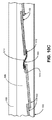
例示的な処理方式として、図3は、本開示の実施形態にかかる、横方向に後退して保護された縁部を有するエミッタ領域を有する太陽電池の形成の平面図を示している。 As an exemplary processing scheme, FIG. 3 shows a plan view of the formation of a solar cell according to an embodiment of the present disclosure, which has an emitter region with a laterally retracted and protected edge.
図3の部分(A)を参照すると、太陽電池の製造方法は、基板300の受光面において、基板300内にエミッタ領域を形成することを含む。部分(B)または(C)を参照すると、エミッタ領域に溝が形成される。パッシベーション層218または268は、基板の受光面上および溝内に形成される。基板は、側壁と、太陽電池の側壁から横方向に後退した側壁を有するエミッタ領域とを有する太陽電池を形成するようにクリーブ加工される。
Referring to the part (A) of FIG. 3, the method for manufacturing a solar cell includes forming an emitter region in the
図3の部分(B)を特に参照すると、実施形態では、基板のクリーブ加工は、図2Aの部分(A)に関連して上述したように、各凹部にパッシベーション層224/226をそれぞれ有するセル302を形成するように溝内のパッシベーション層を通してクリーブ加工することを含む。図3の部分(C)を特に参照すると、他の実施形態では、基板のクリーブ加工は、図2Aの部分(B)に関連して上述したように、各溝にパッシベーション層274/276をそれぞれ有するセル304を形成するように、溝に横方向に隣接するエミッタ領域の一部を通してクリーブ加工することを含む。
With particular reference to the portion (B) of FIG. 3, in the embodiment, the cleaving of the substrate is a cell having a passivation layer 224/226 in each recess, as described above in relation to the portion (A) of FIG. 2A. It involves cleaving through a passivation layer in the groove to form 302. With particular reference to the portion (C) of FIG. 3, in other embodiments, the cleaving of the substrate has a passivation layer 274/276 in each groove, as described above in connection with the portion (B) of FIG. 2A. It involves cleaving through a portion of the emitter region laterally adjacent to the groove so as to form the
実施形態では、基板300のエミッタ領域に溝を形成することは、レーザアブレーションを使用することを含む。他の実施形態では、基板300のエミッタ領域に溝を形成することは、エッチングペーストを使用することを含む。全体として、本開示の1つ以上の実施形態によれば、低照度性能を改善するためにセルを完全に切断または部分的に切断(例えばハーフカット)するためにも使用することができる分離溝を形成するために、レーザまたはエッチングペーストのインクジェットもしくはスクリーンが使用される。実施形態では、セルの拡散長が重ね合わせよりもはるかに小さいため、瓦状の下方の縁部はそれほど重要でない可能性があるが、双方のクリーブ加工された縁部がパッシベーションされる。他の実施形態では、単一の縁部のみが上述したプロセスにしたがってパッシベーションされる。
In the embodiment, forming a groove in the emitter region of the
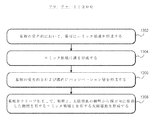
図13は、本発明の実施形態にかかる、太陽電池の製造方法における様々な動作を表すフローチャート1300である。動作1302において、本方法は、基板の受光面において、基板内にエミッタ領域を形成することを含む。動作1304において、本方法は、エミッタ領域に溝を形成することを含む。動作1306において、本方法は、基板の受光面上および溝内にパッシベーション層を形成して、エミッタ縁部をパッシベーションすることを含む。動作1308において、本方法は、基板をクリーブ加工して、側壁と、太陽電池の側壁から横方向に後退した側壁を有するエミッタ領域とを有する太陽電池を形成することを含む。一実施形態では、完全な溝手法が使用される。他の実施形態では、部分溝手法が使用される。
FIG. 13 is a
本開示の1つ以上の実施形態によれば、太陽電池モジュールにおけるシリコン太陽電池の高効率の瓦状配置が本明細書に記載される。例として、図4は、隣接する太陽電池の端部が重なり合って電気的に接続されてスーパーセル400を形成する、瓦状に配置された直列接続太陽電池402のストリングの断面図を示している。各太陽電池402は、半導体ダイオード構造、および光が照射されたときに太陽電池402において生成される電流が外部負荷に供給されることができる半導体ダイオード構造への電気コンタクトを含む。
According to one or more embodiments of the present disclosure, a highly efficient tiled arrangement of silicon solar cells in a solar cell module is described herein. As an example, FIG. 4 shows a cross-sectional view of a string of series-connected
本明細書に記載される例では、各太陽電池402は、n−p接合部の両側に電気コンタクトを提供する前(太陽側)面および背(影側)面メタライゼーションパターンを有する結晶シリコン太陽電池であり、前面メタライゼーションパターンは、n型導電性の半導体層上に配置され、背面メタライゼーションパターンは、p型導電性の半導体層上に配置される。しかしながら、本明細書に記載の太陽電池モジュールにおける太陽電池402の代わりに、またはそれに加えて、任意の他の適切な材料システム、ダイオード構造、物理的寸法、または電気コンタクト配置を採用する任意の他の適切な太陽電池を使用することができる。例えば、前(太陽側)面メタライゼーションパターンは、p型導電性の半導体層上に配置されることができ、背(影側)面メタライゼーションパターンは、n型導電性の半導体層上に配置されることができる。
In the examples described herein, each
再び図4を参照すると、スーパーセル400において、隣接する太陽電池402は、1つの太陽電池の前面メタライゼーションパターンを隣接する太陽電池の背面メタライゼーションパターンに電気的に接続する導電性接合材料によって隣接する太陽電池402が重なり合う領域内で互いに導電接合される。適切な導電性接合材料としては、例えば、導電性接着剤ならびに導電性接着膜および接着テープ、ならびに従来のはんだを挙げることができる。好ましくは、導電性接合材料によって、隣接する太陽電池間の結合に、導電性接合材料の熱膨張係数(CTE)と太陽電池の熱膨張係数(例えば、シリコンのCTE)の不一致から生じる応力を吸収する機械的適合性が提供される。そのような機械的適合性を提供するために、いくつかの変形例では、導電性接合材料は、約0℃以下のガラス転移温度を有するように選択される。CTEの不整合から生じる太陽電池の重なり合う縁部に平行な応力を更に低減して適応させるために、導電性接合材料は、必要に応じて、実質的に太陽電池の縁部の長さを拡張する連続した線ではなく、太陽電池の重なり合う領域に沿った別個の位置にのみ適用されることができる。
Referring again to FIG. 4, in the
太陽電池の前面および背面に垂直に測定された、導電性接合材料によって形成された隣接して重なり合う太陽電池間の導電性結合の厚さは、例えば約0.1mm未満とすることができる。そのような薄い結合は、セル間の相互接続での抵抗損失を低減し、また、動作中に発生する可能性のあるスーパーセルの任意のホットスポットからのスーパーセルに沿った熱の流れを促進する。 The thickness of the conductive bond between adjacent and overlapping solar cells formed by the conductive bonding material, measured perpendicular to the front and back of the solar cell, can be, for example, less than about 0.1 mm. Such thin coupling reduces resistance loss in the interconnection between cells and also facilitates heat flow along the supercell from any hotspot of the supercell that can occur during operation. do.
図5は、スーパーセル400において使用することができる例示的な矩形太陽電池402の前面を示している。適切な場合、太陽電池402の他の形状も使用することができる。すなわち、太陽電池402は、矩形である必要はない。図示の例では、太陽電池402の前面メタライゼーションパターンは、太陽電池402の長辺の1つの縁部に隣接して配置され且つ実質的に長辺の長さにわたって長辺に平行に延びるバスバー500と、バスバーに垂直に取り付けられ且つ実質的に太陽電池402の短辺にわたって互いにおよび短辺に平行に延びるフィンガ502とを含む。
FIG. 5 shows the front surface of an exemplary rectangular
図5の例では、太陽電池402は、約156mmの長さ、約26mmの幅、したがって約1:6のアスペクト比(短辺の長さ/長辺の長さ)を有する。6つのそのような太陽電池は、標準の156mm×156mmの寸法のシリコンウェハ上に作製され、次に分離(ダイシング)されて図示のような太陽電池を提供することができる。他の変形例では、約19.5mm×156mmの寸法、したがって約1:8のアスペクト比を有する8つの太陽電池402を標準的なシリコンウェハから作製することができる。より一般的には、太陽電池402は、例えば、約1:2から約1:20までのアスペクト比を有することができ、標準サイズのウェハまたは任意の他の適切な寸法のウェハから作製されることができる。156.75mm×156.75mm、158.75mm×158.75mm、161.75mm×161.75mm、更にはそれ以上の面積を有するシリコンウェハなど、156mm×156mmよりも大きいシリコンウェハを使用することができることを理解されたい。他の実施形態では、156mm×156mmよりも小さいシリコンウェハを使用することができる。
In the example of FIG. 5, the
図6Aは、前述のように矩形太陽電池を形成するために、標準的なサイズおよび形状の擬似正方形シリコン太陽電池ウェハ600を切断、破壊、または別の方法で分けられることができる例示的な方法を示している。この例では、いくつかの全幅の矩形太陽電池がウェハの中央部から切り出され、更にいくつかのより短い矩形太陽電池402Sがウェハの端部から切り出され、ウェハの面取りまたは丸みを帯びた角が破棄される。太陽電池を使用して、ある幅の瓦状スーパーセルを形成することができ、太陽電池402Sを使用して、より狭い幅の瓦状スーパーセルを形成することができる。
FIG. 6A is an exemplary method in which a pseudo-square silicon
図6Bおよび図6Cは、図6Cに示される破線に沿ってダイシングされて図5に示されるものと同様の前面メタライゼーションパターンを有する複数の太陽電池402を提供することができる擬似正方形ウェハ600と、前面メタライゼーションパターンを有する二つの面取り太陽電池402との正面図および背面図を示している。
6B and 6C are with a
図6Bに示される例示的な前面メタライゼーションパターンでは、別個の接触パッド500を相互接続する薄い導体の2つの端部は、太陽電池の面取り角の周りに延在し、別個の接触パッドが配置される太陽電池の長辺からの距離が増加するにつれて先細りする。そのような先細りは任意であるが、抵抗損失を大幅に増加させることなく、太陽電池の活性領域の金属使用および遮光を有利に低減することができる。
In the exemplary front metallization pattern shown in FIG. 6B, the two ends of the thin conductor interconnecting the
図6Dおよび図6Eは、図5に示されるものと同様の前面メタライゼーションパターンを有する複数の太陽電池402を提供するために、図6Eに示される破線に沿ってダイシングされることができる完全な正方形ウェハ606の正面図および背面図を示している。
6D and 6E are complete that can be diced along the dashed line shown in FIG. 6E to provide multiple
面取りされた矩形太陽電池は、面取り太陽電池のみを含むスーパーセルを形成するために使用することができる。追加的にまたは代替的に、1つ以上のそのような面取りされた矩形太陽電池は、スーパーセルを形成するために、1つ以上の非面取り矩形太陽電池(例えば、図5)と組み合わせて使用することができる。例えば、スーパーセルの端部太陽電池は、面取り太陽電池とすることができ、中間の太陽電池は、非面取り太陽電池であってもよい。面取りされた太陽電池がスーパーセル、またはより一般的には太陽電池モジュールにおいて非面取り太陽電池と組み合わせて使用される場合、太陽電池の動作中に面取り太陽電池および非面取り太陽電池の同じ前面領域が光にさらされることををもたらすような太陽電池の寸法を使用することが望ましいこともある。この方法で太陽電池面積を一致させると、面取り太陽電池および非面取り太陽電池において生成される電流が一致し、これにより、面取り太陽電池および非面取り太陽電池の双方を含む直列接続ストリングの性能が向上する。同じ擬似正方形ウェハから切り出された面取り太陽電池および非面取り太陽電池の面積は、例えば、面取り太陽電池の欠けている角を補うために、ウェハがダイシングされる線の位置を調整して、それらの長軸に垂直な方向において非面取り太陽電池よりも面取り太陽電池を僅かに広くすることによって一致させることができる。 The chamfered rectangular solar cell can be used to form a supercell containing only the chamfered solar cell. Additional or alternative, one or more such chamfered rectangular solar cells are used in combination with one or more non-chamfered rectangular solar cells (eg, FIG. 5) to form a supercell. can do. For example, the end solar cell of the supercell may be a chamfered solar cell, and the intermediate solar cell may be a non-chamfered solar cell. When a chamfered solar cell is used in combination with a non-chafted solar cell in a supercell, or more commonly in a solar cell module, the same front area of the chamfered solar cell and the non-chafted solar cell is present during the operation of the solar cell. It may be desirable to use solar cell dimensions that result in exposure to light. Matching the solar cell areas in this way matches the currents generated by the chamfered and non-chamfered solar cells, which improves the performance of series-connected strings, including both chamfered and non-chamfered solar cells. do. The areas of chamfered and non-chamfered solar cells cut out from the same pseudo-square wafer, for example, by adjusting the position of the lines on which the wafer is diced to make up for the missing corners of the chamfered solar cells, It can be matched by making the chamfered solar cell slightly wider than the non-chamfered solar cell in the direction perpendicular to the major axis.
太陽電池モジュールは、非面取り矩形太陽電池からのみ形成されたスーパーセルのみ、面取り矩形太陽電池から形成されたスーパーセルのみ、もしくは面取り太陽電池および非面取り太陽電池を含むスーパーセルのみ、またはこれら3つのスーパーセルの任意の組み合わせを含むことができる。 The solar cell module is only a supercell formed only from a non-chamfered rectangular solar cell, only a supercell formed from a chamfered rectangular solar cell, or only a supercell containing a chamfered solar cell and a non-chamfered solar cell, or three of these. Any combination of supercells can be included.
場合によっては、ウェハの縁部の近くの標準サイズの正方形または擬似正方形の太陽電池ウェハ(例えば、ウェハ600またはウェハ606)の部分は、縁部から離れて位置するウェハの部分よりも低い効率で光を電気に変換することができる。結果として得られる矩形太陽電池の効率を改善するために、いくつかの変形例では、ウェハがダイシングされる前に、低効率部分を除去するためにウェハの1つ以上の縁部がトリミングされる。ウェハの縁部からトリミングされた部分は、例えば、約1mmから約5mmの幅を有することができる。更に、図6Bおよび図6Cに示されるように、ウェハからダイシングされる2つの端部太陽電池402は、前面バスバー(または別個の接触パッド)500がそれらの外縁部に沿って、したがってウェハの2つの縁部に沿っている状態で配向されることができる。本明細書に開示されるスーパーセルでは、バスバー(または別個の接触パッド)500は、通常、隣接する太陽電池によって重なり合うため、ウェハのこれら2つの縁部に沿った低い光変換効率は、通常、太陽電池の性能に影響を与えない。その結果、いくつかの変形例では、矩形太陽電池の短辺に平行に配向された正方形または擬似正方形ウェハの縁部は、前述のようにトリミングされるが、矩形太陽電池の長辺に平行に配向されたウェハの縁部は、トリミングされない。他の変形例では、正方形ウェハ(例えば、図6Dのウェハ606)の1つ、2つ、3つ、または4つの縁部が、前述したようにトリミングされる。他の変形例では、擬似正方形ウェハの長辺の1つ、2つ、3つ、または4つが、前述したようにトリミングされる。
In some cases, a portion of a standard-sized square or pseudo-square solar cell wafer near the edge of the wafer (eg,
本明細書に開示される太陽電池モジュールにおける抵抗電力損失を低減するために、図示のように、標準の156mm×156mm太陽電池よりも細長いアスペクト比および少ない面積を有する太陽電池を有利に使用することができる。特に、標準サイズのシリコン太陽電池と比較して面積が小さい太陽電池402は、太陽電池において生成される電流の減少をもたらし、これにより、太陽電池およびそのような太陽電池の直列接続ストリングの抵抗電力損失が直接減少する。更に、そのような矩形太陽電池をスーパーセル400に配置して、太陽電池の短辺に平行なスーパーセルに電流が流れるようにすると、電流が前面メタライゼーションパターンのフィンガ502に到達するために半導体材料内を流れなければならない距離を低減することができ、フィンガの必要な長さを短縮することができ、これにより、抵抗電力損失も削減することができる。
In order to reduce the resistance power loss in the solar cell module disclosed herein, it is advantageous to use a solar cell having an elongated aspect ratio and a smaller area than a standard 156 mm × 156 mm solar cell, as shown in the figure. Can be done. In particular, the
上記のように、太陽電池を直列に電気的に接続するために、それらの重なり合う領域において重なり合う太陽電池402を互いに結合すると、太陽電池の従来のタブ付き直列接続ストリングと比較して、隣接する太陽電池間の電気接続の長さが短くなる。これはまた、抵抗電力損失も低減させる。
As described above, in order to electrically connect the solar cells in series, the overlapping
再び図5を参照すると、図示の例では、太陽電池402の前面メタライゼーションパターンは、バスバー500と平行に且つバスバーから間隔を空けて延びる任意のバイパス導体504を含む。(そのようなバイパス導体はまた、必要に応じて、図6Bおよび図6Dに示されているメタライゼーションパターンにおいて使用することもできる)。バイパス導体504は、フィンガ502を相互接続して、バスバー500とバイパス導体504との間に形成され得る亀裂を電気的にバイパスする。そのような亀裂は、バスバー500に近い位置でフィンガ502を切断する可能性があり、そうでなければ、太陽電池402の領域をバスバー500から分離する可能性がある。バイパス導体は、そのような切断されたフィンガとバスバーとの間に代替の電気的経路を提供する。図示された例は、バスバー500に平行に配置され、バスバーのほぼ全長にわたって延在し、且つ全てのフィンガ502を相互接続するバイパス導体504を示している。この配置が好ましい場合もあるが、必須ではない。存在する場合、バイパス導体は、バスバーと平行に延びる必要はなく、バスバーの全長を延在する必要はない。更に、バイパス導体は、少なくとも2つのフィンガを相互接続するが、全てのフィンガを相互接続する必要はない。例えば、長いバイパス導体の代わりに、2つ以上の短いバイパス導体を使用することができる。バイパス導体の任意の適切な配置を使用することができる。
Seeing FIG. 5 again, in the illustrated example, the front metallization pattern of the
図5の例示的な前面メタライゼーションパターンはまた、バスバー500とは反対側の遠端においてフィンガ502を相互接続する任意の端部導体506も含む。(そのような端部導体は、必要に応じて、図6Bおよび図6Dに示されるメタライゼーションパターンにおいて使用することもできる)。導体506の幅は、例えばフィンガ502の幅とほぼ同じにすることができる。導体506は、フィンガ502を相互接続して、バイパス導体504と導体506との間に形成され得る亀裂を電気的にバイパスし、それにより、さもなければそのような亀裂によって電気的に分離される太陽電池402の領域についてのバスバー500への電流経路を提供する。
The exemplary front metallization pattern of FIG. 5 also includes any
図示された例のいくつかは、太陽電池402の長辺の長さを延在する前面バスバー500を実質的に均一な幅で示しているが、これは必須ではない。例えば、上記に暗示されるように、全部バスバー500は、例えば図6Bに示すように、例えば太陽電池402の側面に沿って互いに並べて配置されることができる2つ以上の別個の前面接触パッド500によって置き換えられてもよい。そのような別個の接触パッドは、必要に応じて、例えば前述した図における例に示されるように、それらの間を延びるより細い導体によって相互接続されることができる。そのような変形例では、太陽電池の長辺に対して垂直に測定された接触パッドの幅は、例えば、接触パッドを相互接続する細い導体の幅の約2倍から約20倍とすることができる。前面メタライゼーションパターン内の各フィンガに別個の(例えば、小さな)接触パッドが存在してもよく、各接触パッドが2つ以上のフィンガに接続されてもよい。前面接触パッド500は、例えば、正方形であってもよく、または太陽電池の縁部に平行に細長い矩形の形状を有してもよい。前面接触パッド500は、太陽電池の長辺に垂直な例えば約1mmから約1.5mmの幅、および、太陽電池の長辺に平行な例えば約1mmから約10mmの長さを有することができる。太陽電池の長辺に平行に測定された接触パッド500間の間隔は、例えば、約3mmから約30mmとすることができる。
Some of the illustrated examples show the
あるいは、太陽電池402は、前部バスバー500および別個の前面接触パッド500の双方を欠いていてもよく、前面メタライゼーションパターンにフィンガ502のみを含んでもよい。そのような変形例では、そうでなければ前部バスバー500または接触パッド500によって実行されるであろう電流収集機能は、代わりに、上述した重なり合う構成において2つの太陽電池402を互いに結合するために使用される導電性材料によって実行されるかまたは部分的に実行されることができる。
Alternatively, the
バスバー500および接触パッド500の双方を欠く太陽電池は、バイパス導体504を含むか、またはバイパス導体504を含まないかのいずれかとすることができる。バスバー500および接触パッド500が存在しない場合、バイパス導体504は、バイパス導体と、重なり合う太陽電池に導電結合される前面メタライゼーションパターンの部分との間に形成される亀裂をバイパスするように配置されることができる。
A solar cell lacking both the
バスバーまたは別個の接触パッド500、フィンガ502、バイパス導体504(存在する場合)、および端部導体506(存在する場合)を含む前面メタライゼーションパターンは、例えば、そのような目的のために従来使用される銀ペーストから形成され、例えば、従来のスクリーン印刷法によって蒸着されることができる。あるいは、前面メタライゼーションパターンは、電気めっきされた銅から形成されることができる。任意の他の適切な材料およびプロセスも使用することができる。前面メタライゼーションパターンが銀から形成されている変形例では、セルの縁部に沿った連続バスバー500ではなく、別個の前面接触パッド500を使用すると、太陽電池上の銀の量が減り、コストを有利に削減することができる。前面メタライゼーションパターンが銅からまたは銀よりも安価な他の導体から形成される変形例では、コストの不利益なしに連続バス500を使用することができる。
Front metallization patterns, including busbars or
図6Cおよび図6Eは、太陽電池の例示的な背面メタライゼーションパターンを示している。これらの例では、背面メタライゼーションパターンは、太陽電池の背面の長辺の1つに沿って配置された別個の背面接触パッド602と、太陽電池の残りの背面の実質的に全てを覆う金属コンタクト604とを含む。瓦状スーパーセルでは、接触パッド602は、2つの太陽電池を直列に電気的に接続するために、例えば隣接して重なり合う太陽電池の上面の縁部に沿って配置されたバスバーまたは別個の接触パッドに結合される。例えば、別個の各背面接触パッド602は、別個の接触パッドにのみ適用される導電性接合材料によって、重なり合う太陽電池の前面の対応する別個の前面接触パッド500と位置合わせされて結合されることができる。別個の接触パッド602は、例えば、正方形であってもよく、または太陽電池の縁部に平行に細長い矩形形状を有してもよい(例えば、図6Cおよび図6E)。接触パッド602は、太陽電池の長辺に垂直な例えば約1mmから約5mmの幅、および、太陽電池の長辺に平行な例えば約1mmから約10mmの長さを有することができる。太陽電池の長辺に平行に測定された接触パッド602間の間隔は、例えば、約3mmから約30mmとすることができる。
6C and 6E show exemplary back metallization patterns for solar cells. In these examples, the back metallization pattern is a separate
コンタクト604は、例えば、アルミニウムおよび/または電気めっきされた銅から形成されることができる。アルミニウム背面コンタクト604の形成は、通常、太陽電池内の背面再結合を低減する背面電界を提供し、それにより太陽電池効率を改善する。コンタクト604がアルミニウムではなく銅から形成される場合、コンタクト604は、同様に背面再結合を低減するために、他のパッシベーション方式(例えば、酸化アルミニウム)と組み合わせて使用することができる。別個の接触パッド602は、例えば銀ペーストから形成されることができる。セルの縁部に沿った連続的な銀接触パッドではなく、別個の銀接触パッド602を使用すると、背面メタライゼーションパターンの銀の量が減少し、有利にコストを削減することができる。
The
更に、太陽電池が背面コンタクトの再結合を低減するためにアルミニウムコンタクトの形成によって提供される背面電界に依存している場合、連続的な銀コンタクトではなく別個の銀コンタクトを使用すると、太陽電池の効率を向上させることができる。これは、銀の背面コンタクトが背面電界を提供しないため、キャリアの再結合を促進して銀コンタクト上の太陽電池に不感(非活性)容積を生成する傾向があるためである。従来のリボンタブ付き太陽電池ストリングでは、それらの不感容積は、通常、太陽電池の前面のリボンおよび/またはバスバーによって遮光されているため、効率の余分な損失をもたらさない。しかしながら、本明細書に開示される太陽電池およびスーパーセルでは、背面銀接触パッド602上の太陽電池の容積は、通常、いかなる前面メタライゼーションによっても遮光されておらず、銀背面メタライゼーションの使用に起因するいかなる不感容積も、セルの効率を低減させる。したがって、太陽電池の背面の縁部に沿った連続的な銀接触パッドではなく、別個の銀接触パッド602を使用すると、いかなる対応する不感帯の容積も減少し、太陽電池の効率を向上させる。
In addition, if the solar cell relies on the backside electric field provided by the formation of aluminum contacts to reduce recombination of the backside contacts, using a separate silver contact instead of a continuous silver contact will result in the solar cell's Efficiency can be improved. This is because the silver back contacts do not provide a back electric field, which tends to promote carrier recombination and create insensitive (inactive) volumes in the solar cells on the silver contacts. In conventional solar cell strings with ribbon tabs, their dead volume is usually shielded by the ribbon and / or busbar on the front of the solar cell, thus not resulting in an extra loss of efficiency. However, in the solar cells and supercells disclosed herein, the volume of the solar cell on the back
図に示される特定の例の太陽電池は、前面および背面のメタライゼーションパターンの特定の組み合わせを有するものとして説明されているが、より一般的には、前面および背面のメタライゼーションパターンの任意の適切な組み合わせを使用することができる。例えば、1つの適切な組み合わせは、別個の接触パッド500、フィンガ502、および任意のバイパス導体504を含む銀前面メタライゼーションパターン、ならびにアルミニウムコンタクト604および別個の銀接触パッド602を含む背面メタライゼーションパターンを使用することができる。他の適切な組み合わせは、連続バスバー500、フィンガ502、および任意のバイパス導体504を含む銅前面メタライゼーションパターン、ならびに連続バスバー602および銅コンタクト604を含む背面メタライゼーションパターンを使用することができる。より一般的には、太陽電池402は、任意の適切な前面および背面メタライゼーションパターンを使用することができる。
The particular example solar cell shown in the figure is described as having a particular combination of front and back metallization patterns, but more generally any suitable front and back metallization patterns. Combinations can be used. For example, one suitable combination is a silver front metallization pattern that includes a
図7は、図4に示すように瓦状に配置された図5に示すような太陽電池402を含む例示的な矩形スーパーセル400の前面の一部を示している。瓦状形状の結果、太陽電池402の対間に物理的な間隙はない。更に、スーパーセル400の一端にある太陽電池402のバスバー500が見えるが、他の太陽電池のバスバー(または前面接触パッド)は、隣接する太陽電池の重なり合う部分の下方に隠れている。結果として、スーパーセル400は、太陽電池モジュールで占める領域を効率的に使用する。特に、その領域のうち、従来のタブ付き太陽電池配置、および太陽電池の照射される表面上に多数の視認可能なバスバーを含む太陽電池配置の場合よりも大きい部分が電気を生成するために利用可能である。
FIG. 7 shows a portion of the front surface of an exemplary
図7に示される例では、バイパス導体504は、隣接するセルの重なり合う部分によって隠されている。あるいは、バイパス導体504を含む太陽電池は、バイパス導体を覆わずに図7に示されるものと同様に重なり合うことができる。
In the example shown in FIG. 7, the
スーパーセル400の一端にある露出した前面バスバー500、およびスーパーセル400の他端にある太陽電池の背面メタライゼーションは、スーパーセル400を他のスーパーセルおよび/または他の電気部品に必要に応じて電気的に接続するために使用することができるスーパーセルの負および正(端子)端部コンタクトを提供する。
The exposed
スーパーセル400内の隣接する太陽電池は、任意の適切な量、例えば約1ミリメートル(mm)から約5mmだけ重なり合うことができる。
Adjacent solar cells within the
例えば、図8A〜図8Dに示すように、前述した瓦状スーパーセルは、太陽電池モジュールの領域を効率的に埋めることができる。そのような太陽電池モジュールは、例えば正方形または矩形とすることができる。図8A〜図8Dに示されるような矩形太陽電池モジュールは、例えば約1メートルの長さを有する短辺と、例えば約1.5から約2.0メートルの長さを有する長辺とを有することができる。太陽電池モジュールに適した任意の他の形状および寸法も使用することができる。太陽電池モジュール内のスーパーセルの任意の適切な配置を使用することができる。 For example, as shown in FIGS. 8A to 8D, the tile-shaped supercell described above can efficiently fill the area of the solar cell module. Such solar cell modules can be, for example, square or rectangular. A rectangular solar cell module as shown in FIGS. 8A-8D has, for example, a short side having a length of about 1 meter and a long side having a length of, for example, about 1.5 to about 2.0 meters. be able to. Any other shape and size suitable for the solar cell module can also be used. Any suitable arrangement of supercells within the solar cell module can be used.
正方形または矩形太陽電池モジュールでは、スーパーセルは、通常、太陽電池モジュールの短辺または長辺に平行な列に配置される。各列は、端同士をつないで配置された1つ、2つ、またはそれ以上のスーパーセルを含むことができる。そのような太陽電池モジュールの一部を形成するスーパーセル400は、任意の適切な数の太陽電池402を含むことができ、任意の適切な長さからなることができる。いくつかの変形例では、スーパーセル400は、それぞれ、それらが一部となっている矩形太陽電池モジュールの短辺の長さにほぼ等しい長さを有する。他の変形例では、スーパーセル400は、それぞれ、それらが一部となっている矩形太陽電池モジュールの短辺の長さの半分にほぼ等しい長さを有する。他の変形例では、スーパーセル400は、それぞれ、それらが一部となっている矩形太陽電池モジュールの長辺の長さにほぼ等しい長さを有する。他の変形例では、スーパーセル400は、それぞれ、それらが一部となっている矩形太陽電池モジュールの長辺の長さの半分にほぼ等しい長さを有する。これらの長さのスーパーセルを作製するのに必要な太陽電池の数は、もちろん、太陽電池モジュールの寸法、太陽電池の寸法、および隣接する太陽電池が重なり合う量に依存する。スーパーセルに適した任意の他の長さも使用することができる。
In a square or rectangular solar cell module, the supercells are typically arranged in a row parallel to the short or long side of the solar cell module. Each column can contain one, two, or more supercells arranged end-to-end. The
スーパーセル400が矩形太陽電池モジュールの短辺の長さにほぼ等しい長さを有する変形例では、スーパーセルは、例えば、隣接する太陽電池が約3mmだけ重なり合う、約19.5ミリメートル(mm)×約156mmの寸法を有する56個の矩形の太陽電池を含むことができる。従来の正方形または擬似正方形の156mmウェハから8個のそのような矩形太陽電池が分離されることができる。あるいは、そのようなスーパーセルは、例えば、隣接する太陽電池が約2mmだけ重なり合う、約26mm×約156mmの寸法を有する38個の矩形太陽電池を含むことができる。従来の正方形または擬似正方形の156mmウェハから6個のそのような矩形太陽電池が分離されることができる。スーパーセル400が矩形太陽電池モジュールの短辺の長さのほぼ半分の長さを有する変形例では、スーパーセルは、例えば、隣接する太陽電池が約3mmだけ重なり合う、約19.5ミリメートル(mm)×約156mmの寸法を有する28個の矩形太陽電池を含むことができる。あるいは、そのようなスーパーセルは、例えば、隣接する太陽電池が約2mmだけ重なり合う、約26mm×約156mmの寸法を有する19個の矩形の太陽電池を含むことができる。
In a variant in which the
スーパーセル400が矩形太陽電池モジュールの長辺の長さにほぼ等しい長さを有する変形例では、スーパーセルは、例えば、隣接する太陽電池が約2mmだけ重なり合う、約26mm×約156mmの寸法を有する72個の矩形太陽電池を含むことができる。スーパーセル400が矩形太陽電池モジュールの長辺の長さの半分にほぼ等しい長さを有する変形例では、スーパーセルは、例えば、隣接する太陽電池が約2mmだけ重なり合う、約26mm×約156mmの寸法を有する36個の矩形太陽電池を含むことができる。
In a variant in which the
図8Aは、それぞれが太陽電池モジュールの短辺の長さの半分にほぼ等しい長さを有する20個の矩形スーパーセル400を含む例示的な矩形太陽電池モジュール800を示している。スーパーセルは、端同士をつないで対で配置され、10列のスーパーセルを形成し、スーパーセルの列および長辺は、太陽電池モジュールの短辺と平行に配向されている。他の変形例では、スーパーセルの各列は、3つ以上のスーパーセルを含むことができる。また、同様に構成された太陽電池モジュールは、この例に示すよりも多いまたは少ないスーパーセルの列を含むことができる。
FIG. 8A shows an exemplary rectangular solar cell module 800, each containing 20
それらの少なくとも1つが列内の他のスーパーセルに隣接するスーパーセルの端部に前面端部コンタクトを有するように各列のスーパーセルが配置される変形例では、間隙は、太陽電池モジュールの中心線に沿ったスーパーセル400の前面端部コンタクトへの電気接触を容易にすることができることを理解されたい。例えば、列内の2つのスーパーセルは、一方のスーパーセルが太陽電池モジュールの中心線に沿って前面端子コンタクトを有し、他方のスーパーセルが太陽電池モジュールの中心線に沿って背面端子コンタクトを有するように配置されることができる。そのような配置では、列内の2つのスーパーセルは、太陽電池モジュールの中心線に沿って配置され且つ一方のスーパーセルの前面端子コンタクトおよび他方のスーパーセルの背面端子コンタクトに結合された相互接続によって直列に電気的に接続されることができる。(例えば、以下の図10Cを参照)。スーパーセルの各列が3つ以上のスーパーセルを含む変形例では、スーパーセル間に追加の間隙が存在してもよく、同様に、太陽電池モジュールの側面から離れた場所にある前面端部コンタクトへの電気接触を容易にすることができる。
In a variant in which the supercells in each row are arranged so that at least one of them has a front end contact at the end of the supercell adjacent to the other supercell in the row, the gap is the center of the solar cell module. It should be appreciated that electrical contact with the front end contact of the
図8Bは、それぞれが太陽電池モジュールの短辺の長さにほぼ等しい長さを有する10個の矩形スーパーセル400を含む例示的な矩形太陽電池モジュール803を示している。スーパーセルは、それらの長辺がモジュールの短辺と平行に配向されるように10個の平行な列として配置される。同様に構成された太陽電池モジュールは、この例に示されているよりも多いまたは少ない横長のスーパーセルの列を含むことができる。
FIG. 8B shows an exemplary rectangular solar cell module 803, each containing ten
図8Bはまた、太陽電池モジュール800内のスーパーセルの列内の隣接するスーパーセル間に間隙がない場合の図8Aの太陽電池モジュール800の外観を示している。例えば、各列の双方のスーパーセルがモジュールの中心線に沿って背面端部コンタクトを有するようにスーパーセルを配置することによって、間隙の使用を省略することができることを理解されたい。この場合、モジュールの中心に沿ってスーパーセルの前面にアクセスする必要がないため、スーパーセルは、ほとんどまたは全く余計な間隙を有さずに互いにほとんど当接して配置されることができる。あるいは、列内の2つのスーパーセル400は、一方がモジュールの側面に沿った前面端部コンタクトおよびモジュールの中心線に沿った背面端部コンタクトを有し、他方がモジュールの中心線に沿った前面端部コンタクトおよびモジュールの反対側の側面に沿った背面端部コンタクトを有し、且つスーパーセルの隣接する端部が重なり合うように配置されることができる。可撓性相互接続部は、スーパーセルの一方の前面端部コンタクトおよび他方のスーパーセルの背面端部コンタクトへの電気接続を提供するために、太陽電池モジュールの前面の任意の部分を遮光せずに、スーパーセルの重なり合う端部の間に挟持されることができる。3つ以上のスーパーセルを含む列の場合、これら2つの手法を組み合わせて使用することができる。
FIG. 8B also shows the appearance of the solar cell module 800 of FIG. 8A when there is no gap between adjacent supercells in the row of supercells in the solar cell module 800. It should be appreciated that the use of gaps can be omitted, for example, by arranging the supercells so that both supercells in each row have back edge contacts along the centerline of the module. In this case, since it is not necessary to access the front surface of the supercell along the center of the module, the supercells can be arranged so that they are almost in contact with each other with little or no extra clearance. Alternatively, two
図8Aおよび図8Bに示すスーパーセルおよびスーパーセルの列は、直列および並列の電気接続の任意の適切な組み合わせによって相互接続されることができる。スーパーセル間の相互接続は、例えば、図8Cおよび図8Dに関して以下に説明されるのと同様に、可撓性相互接続部を使用して行うことができる。 The supercells and columns of supercells shown in FIGS. 8A and 8B can be interconnected by any suitable combination of series and parallel electrical connections. The interconnection between supercells can be made using flexible interconnects, for example, as described below with respect to FIGS. 8C and 8D.
図8Cは、それぞれが太陽電池モジュールの長辺の長さにほぼ等しい長さを有する6個の矩形スーパーセル400を含む例示的な矩形太陽電池モジュール804を示している。スーパーセルは、それらの長辺がモジュールの長辺に平行になるように6個の平行な列として配置される。同様に構成された太陽電池モジュールは、この例に示されているよりも多いまたは少ない横長のスーパーセルの列を含むことができる。この例(および以下の例のいくつか)の各スーパーセルは、それぞれが156mmの正方形または擬似正方形ウェハの幅の約1/6に等しい幅を有する72個の矩形太陽電池を含む。任意の他の適切な寸法の任意の他の適切な数の矩形太陽電池も使用することができる。この例では、スーパーセルの前面端子コンタクトは、モジュールの一方の短辺の縁部に隣接して配置され且つそれと平行に延びる可撓性相互接続部806によって互いに電気的に接続されている。スーパーセルの背面端子コンタクトは、太陽電池モジュールの後方にある他方の短辺の縁部に隣接して配置され且つそれと平行に延びる可撓性相互接続部によって同様に互いに接続されている。背面相互接続は、図8Cの表示から隠れている。この配置により、6個のモジュール長のスーパーセルは並列に電気的に接続される。
FIG. 8C shows an exemplary rectangular
図8Dは、それぞれが太陽電池モジュールの長辺の長さの半分にほぼ等しい長さを有する12個の矩形のスーパーセル400を含む例示的な矩形太陽電池モジュール812を示している。スーパーセルは、端同士をつないで対で配置され、6列のスーパーセルを形成し、スーパーセルの列および長辺は、太陽電池モジュールの長辺と平行に配向されている。他の変形例では、スーパーセルの各列は、3つ以上のスーパーセルを含むことができる。また、同様に構成された太陽電池モジュールは、この例に示すよりも多いまたは少ないスーパーセルの列を含むことができる。この例(および以下の例のいくつか)の各スーパーセルは、それぞれが156mmの正方形または擬似正方形ウェハの幅の約1/6に等しい幅を有する36個の矩形太陽電池を含む。任意の他の適切な寸法の任意の他の適切な数の矩形太陽電池も使用することができる。太陽電池モジュールの中心線に沿ったスーパーセル400の前面端部コンタクトへの電気的接触を容易にするために間隙を使用することができることを理解されたい。この例では、モジュールの一方の短辺の縁部に隣接して配置され且つそれと平行に延びる可撓性相互接続部806は、6個のスーパーセルの前面端子コンタクトを電気的に相互接続する。同様に、モジュールの背後にあるモジュールの他方の短辺の縁部に隣接して配置され且つそれと平行に延びる可撓性相互接続部は、他の6個のスーパーセルの背面端子コンタクトを電気的に接続する。可撓性相互接続部(この図には示されていない)は、列のスーパーセルの各対の間隙に沿って直列に配置されることができ、必要に応じて、横方向に延びて隣接する列を並列に相互接続することができる。この配置により、6列のスーパーセルは並列に電気的に接続される。必要に応じて、スーパーセルの第1のグループでは、各列の第1のスーパーセルは、他の各列の第1のスーパーセルと電気的に並列に接続され、スーパーセルの第2のグループでは、第2のスーパーセルは、他の各列の第2のスーパーセルと電気的に並列に接続され、スーパーセルの2つのグループは、電気的に直列に接続されている。後者の配置は、スーパーセルの2つのグループのそれぞれを個別にバイパスダイオードと並列に配置することができる。
FIG. 8D shows an exemplary rectangular
図8Dの詳細Aは、モジュールの1つの短辺の縁部に沿ったスーパーセルの背面端子コンタクトの相互接続の図10Aに示す断面図の位置を示している。同様に、詳細Bは、モジュールの他の短辺の縁部に沿ったスーパーセルの前面端子コンタクトの相互接続の図10Bに示す断面図の位置を示している。詳細Cは、間隙808に沿った列内のスーパーセルの直列相互接続の図10Cに示される断面図の位置を示している。
Detail A of FIG. 8D shows the location of the cross-sectional view shown in FIG. 10A of the interconnection of the back terminal contacts of the supercell along the edge of one short side of the module. Similarly, detail B shows the location of the cross-sectional view shown in FIG. 10B of the interconnection of the front terminal contacts of the supercell along the edges of the other short sides of the module. Detail C shows the position of the cross section shown in FIG. 10C of the series interconnection of supercells in a row along the
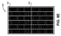
他の例では、ハーフカット太陽電池が太陽電池モジュールの製造に使用される。図8Eは、本開示の実施形態にかかる、ハーフカットセルを含む太陽電池モジュールの平面図を示し、図8Fは、図8Eの太陽電池モジュールの一部の拡大図を示している。 In another example, half-cut solar cells are used in the manufacture of solar cell modules. FIG. 8E shows a plan view of the solar cell module including the half-cut cell according to the embodiment of the present disclosure, and FIG. 8F shows an enlarged view of a part of the solar cell module of FIG. 8E.
図8Eおよび図8Fを参照すると、モジュール820は、ハーフカット太陽電池822を含む。一実施形態では、図8Fに示すように、セルは、上向きハーフカットセル822Aおよび下向きハーフカットセル822Bの交互の列に配置される。図8Eに描かれているように、モジュール820の配置に中心線824を含めることができる。他の実施形態では、そのような中心線は含まれない。
With reference to FIGS. 8E and 8F,
他の瓦状モジュール構成が製造されることができることを理解されたい。例として、図8Gは、本開示の実施形態にかかる、矩形ストリップ配置を有する垂直瓦状レイアップを含む太陽電池モジュールの平面図を示している。図8Gを参照すると、モジュール830は、矩形太陽電池834の垂直ストリップ832を含む。
It should be understood that other tiled module configurations can be manufactured. As an example, FIG. 8G shows a plan view of a solar cell module including a vertical tile-like layup with a rectangular strip arrangement according to an embodiment of the present disclosure. Referring to FIG. 8G, module 830 includes a
他の例として、図8Hは、本開示の実施形態にかかる、瓦状の面取りされたセル配置を有する垂直レイアップを含む太陽電池モジュールの平面図を示している。図8Hを参照すると、モジュール840は、面取り太陽電池842の垂直ストリップを含む。
As another example, FIG. 8H shows a plan view of a solar cell module according to an embodiment of the present disclosure, which includes a vertical layup with a tiled chamfered cell arrangement. Referring to FIG. 8H,
他の例として、図8Iは、本開示の実施形態にかかる、瓦状セルおよび中心線配置を有する垂直レイアップを含む太陽電池モジュールの平面図を示している。図8Iを参照すると、モジュール850は、面取り太陽電池854の垂直ストリップ852を含む。他の実施形態では、矩形セルが使用される。図示のように、中心線856は、モジュール850の配置に含まれることができる。他の実施形態では、そのような中心線は含まれない。
As another example, FIG. 8I shows a plan view of a solar cell module according to an embodiment of the present disclosure, which includes a tiled cell and a vertical layup with a centerline arrangement. With reference to FIG. 8I,
図9は、図8Cおよび図8Dよりも詳細に、各列内のスーパーセルを互いに直列に配置し且つ列を互いに並列に配置するように可撓性電気相互接続によって相互接続された3列のスーパーセルの例示的な配置を示している。これらは、例えば、図8Dの太陽電池モジュールの3列とすることができる。図9の例では、各スーパーセル400は、その前面端子コンタクトに導電接合した可撓性相互接続部806と、その背面端子コンタクトに導電接合した他の可撓性相互接続部とを有する。各列内の2つのスーパーセルは、一方のスーパーセルの前面端子コンタクトおよび他方のスーパーセルの背面端子コンタクトに導電接合した共有可撓性相互接続部によって直列に電気的に接続される。各可撓性相互接続部は、それが結合されているスーパーセルの端部に隣接して配置され且つそれと平行に延び、スーパーセルを超えて横方向に延びて、隣接する列のスーパーセルの可撓性相互接続部に導電接合し、隣接する列を電気的に並列に接続することができる。図9の破線は、スーパーセルの一部を覆うことで表示から隠されている可撓性相互接続部の部分、または可撓性相互接続部の部分を覆うことで表示から隠されているスーパーセルの部分を示している。
FIG. 9 shows, in more detail than FIGS. 8C and 8D, three rows interconnected by flexible electrical interconnects such that the supercells in each row are arranged in series with each other and the columns are arranged in parallel with each other. An exemplary arrangement of supercells is shown. These can be, for example, three rows of solar cell modules of FIG. 8D. In the example of FIG. 9, each
可撓性相互接続部806は、例えば、重なり合う太陽電池の接合に使用するための上述した機械的適合性のある導電性接合材料を用いてスーパーセルに導電接合されることができる。必要に応じて、導電性接合材料は、導電性接合材料または相互接続部の熱膨張係数とスーパーセルの熱膨張係数との不一致から生じるスーパーセルの縁部に平行な応力を低減するかまたはそれに適応するために、スーパーセルの縁部の長さを実質的に延在する連続線ではなく、スーパーセルの縁部に沿った離散位置にのみ配置されることができる。
The
可撓性相互接続部806は、例えば、薄い銅シートから形成されるかまたはそれを含むことができる。可撓性相互接続部806は、必要に応じて、相互接続部のCTEとスーパーセルのCTEとの間の不一致から生じるスーパーセルの縁部に垂直および平行な応力を低減するかまたはそれに適応するために、スーパーセルの縁部に垂直および平行の双方の機械的適合性(可撓性)を高めるように、パターニングされるかまたは別の方法で構成されることができる。そのようなパターニングは、例えば、スリット、スロット、または孔を含むことができる。相互接続部806の導電性部分は、相互接続部の可撓性を高めるために、例えば、約100ミクロン未満、約50ミクロン未満、約30ミクロン未満、または約25ミクロン未満の厚さを有することができる。可撓性相互接続部の機械的適合性、およびそのスーパーセルへの接合は、相互接続されたスーパーセルが、瓦状太陽電池モジュールの製造方法に関して以下により詳細に説明する積層プロセス中のCTE不一致から生じる応力に耐え、約−40℃から約85℃の温度サイクル試験中のCTE不一致から生じる応力に耐えるのに十分でなければならない。好ましくは、可撓性相互接続部806は、それらが接合されるスーパーセルの端部に平行な電流に対して、約0.015オーム以下、約0.012オーム以下、または約0.01オーム以下の抵抗を示す。
The
例えば、図10A〜図10Cの断面図に示すように、本明細書に記載の太陽電池モジュールは、通常、スーパーセルと、透明な前面シート1000と背面シート1002との間に挟持された1つ以上のカプセル材料808との積層構造を含む。透明な前面シートは、例えばガラスとすることができる。必要に応じて、背面シートも透明にすることができ、これは、太陽電池モジュールの両面動作を可能にすることができる。背面シートは、例えばポリマーシートとすることができる。あるいは、太陽電池モジュールは、前面および背面シートガラスの双方を有するガラス−ガラスモジュールとすることができる。
For example, as shown in the cross-sectional views of FIGS. 10A-10C, the solar cell module described herein is usually one sandwiched between a supercell and a
図10Aの断面図(図8Dの詳細A)は、太陽電池モジュールの前面から隠された、太陽電池モジュールの縁部の近くのスーパーセルの背面端子コンタクトに導電接合し且つスーパーセルの下方に内向きに延在する可撓性相互接続部806の例を示している。図示のように、相互接続部806とスーパーセルの背面との間にカプセル材1004の余分なストリップが配置されることができる。図示のように、接着またははんだ付けされた接合部1006も含むことができる。
A cross-sectional view of FIG. 10A (detail A of FIG. 8D) is conductively bonded to the rear terminal contact of the supercell near the edge of the solar cell module and inside below the supercell, hidden from the front surface of the solar cell module. An example of a
図10Bの断面図(図8Bの詳細B)は、スーパーセルの前面端子コンタクトに導電接合した可撓性相互接続部806の例を示している。図示のように、接着またははんだ付けされた接合部1008も含むことができる。
The cross-sectional view of FIG. 10B (detail B of FIG. 8B) shows an example of a
図10Cの断面図(図8Bの詳細C)は、2つのスーパーセルを直列に電気的に接続するために、一方のスーパーセルの前面端子コンタクトおよび他方のスーパーセルの背面端子コンタクトに導電接合した共有可撓性相互接続部806の例を示している。任意の黒色フィルムまたはコーティング1014が相互接続部に含まれることができる。図示のように、接着またははんだ付けされた接合部1010および/または1012も含むことができる。
The cross-sectional view of FIG. 10C (detail C of FIG. 8B) is conductively bonded to the front terminal contact of one supercell and the back terminal contact of the other supercell in order to electrically connect the two supercells in series. An example of the shared
実施形態によれば、上部リボンが隣り合うモジュールによって覆われるように、モジュール自体が瓦状にされてもよい。図11は、そのような配置1100の簡略化された断面図を示しており、隣接するモジュール1102の端部1101は、インスタントモジュール1106の上部リボン1104と重なり合うように機能する。各モジュール自体は、複数の瓦状太陽電池1107を含む。インスタントモジュール1106の下部リボン1108は埋められている。インスタントモジュール1106の下部リボン1108は、次の隣接する瓦状モジュールと重なり合うように、インスタントの瓦状モジュールの高い側に位置する。この瓦状モジュール構成はまた、モジュールアレイの最終的な露出領域に悪影響を与えることなく、モジュール上の他の要素の追加領域を提供することもできる。重なり合う領域に配置されることができるモジュール要素の例は、これらに限定されるものではないが、接続箱(jボックス)1110および/またはバスリボンを含むことができる。
According to embodiments, the modules themselves may be tiled so that the upper ribbon is covered by adjacent modules. FIG. 11 shows a simplified cross-sectional view of such an
図12は、瓦状モジュール構成1200の他の実施形態を示している。ここで、それぞれの隣接する瓦状モジュール1206および1208のjボックス1202、1204は、それらの間の電気的接続を達成するために嵌合配置1210にある。これは、配線をなくすことによって瓦状モジュールのアレイの構成を簡略化する。特定の実施形態では、jボックスは、補強されることができ、且つ/または追加の構造的スタンドオフと組み合わせることができる。そのような構成は、統合された傾斜モジュールルーフマウントラックの解決策を形成することができ、接続箱の寸法は傾斜を決定する。そのような実装は、瓦状モジュールのアレイが平らな屋根に取り付けられている場合に特に役立つことができる。モジュールがガラス基板およびガラスカバーを含む場合(ガラス−ガラスモジュール)、モジュールは、モジュール全体の長さ(したがって、瓦状にすることにより生じる露出長さL)を短くすることにより、追加のフレーム部材なしで使用することができる。そのような短縮により、傾斜アレイのモジュールは、歪みのもとで割れることなく、予想される物理的負荷(例えば、5400Paの雪荷重制限)に耐えることができる。
FIG. 12 shows another embodiment of the
瓦状に組み立てられた複数の個々の太陽電池を含むスーパーセル構造の使用は、物理的負荷および他の要件によって決定される特定の長さを満たすためにモジュールの長さの変更に容易に適応することができることを理解されたい。 The use of a supercell structure containing multiple individual solar cells assembled in a tile is easily adapted to module length changes to meet specific lengths determined by physical load and other requirements. Please understand that you can.
太陽電池を製造するために、上述した1つ以上のプロセスを実装することができることも理解されたい。上述したプロセスは、太陽電池を製造するために、全体として、または上述した1つ以上のプロセスの一部として実装されることができる。前面接触太陽電池について上記詳細に説明したが、相互嵌合背面接触(IBC)太陽電池製造プロセスも、本明細書に開示された実施形態を実装することによって利益を得ることができることを理解されたい。 It should also be appreciated that one or more of the processes described above can be implemented to manufacture solar cells. The processes described above can be implemented as a whole or as part of one or more of the processes described above to manufacture a solar cell. Although the front contact solar cells have been described in detail above, it should be understood that the interconnected back contact (IBC) solar cell manufacturing process can also benefit from implementing the embodiments disclosed herein. ..
特定の材料が上述の実施形態に関連して具体的に記載されているが、いくつかの材料は、他の実施形態が本開示の実施形態の趣旨及び範囲内に留まる限り、そのような実施形態の他のもので容易に置き換えられることができる。例えば、一実施形態では、異なる材料基板(例えばIII〜V族材料基板)を、シリコン基板の代わりに用いることができる。更にまた、太陽電池の背面のエミッタ領域に関して、P+型ドーピングの後にN+型ドーピングとする順序が特に記載されている場合、想定される他の実施形態は、導電型の反対の順序、すなわち、それぞれ、N+型ドーピングの後にP+型ドーピングを含むことを理解すべきである。他の実施形態では、N型ドープ基板の代わりにP型ドープ基板が使用される。他の実施形態では、上述した手法は、太陽電池以外の製造に適用可能とすることができる。例えば、発光ダイオード(LED)の製造は、本明細書に記載の手法から利益を得ることができる。 Although certain materials are specifically described in connection with the embodiments described above, some materials are such embodiments as long as other embodiments remain within the spirit and scope of the embodiments of the present disclosure. It can be easily replaced by other forms. For example, in one embodiment, different material substrates (eg, group III-V material substrates) can be used in place of the silicon substrates. Furthermore, with respect to the emitter region on the back of the solar cell, if the order of P + type doping followed by N + type doping is specifically described, the other possible embodiments are in the opposite order of the conductive type, i.e., respectively. It should be understood that P + type doping is included after N + type doping. In other embodiments, a P-type dope substrate is used instead of the N-type dope substrate. In other embodiments, the techniques described above can be made applicable to manufacturing other than solar cells. For example, the manufacture of light emitting diodes (LEDs) can benefit from the techniques described herein.
したがって、クリーブ加工された縁部から後退した接合部を有する太陽電池を製造する方法、および結果として得られる太陽電池が開示されてきた。 Therefore, methods for making solar cells with joints recessed from the cleaved edges and the resulting solar cells have been disclosed.
具体的な実施形態が上述されてきたが、これらの実施形態は、特定の機能に関して単一の実施形態のみが説明される場合であっても、本開示の範囲を限定することを意図するものではない。本開示で提供される特徴の例は、別段の記述がある場合を除き、制約的であることよりも、むしろ例示的であることを意図するものである。上記の説明は、本開示から利益を得る当業者には明らかとなるような、代替形態、変更形態、および均等物を包含することを意図するものである。 Although specific embodiments have been described above, these embodiments are intended to limit the scope of the present disclosure, even if only a single embodiment is described for a particular function. is not it. The examples of features provided in this disclosure are intended to be exemplary rather than restrictive, unless otherwise stated. The above description is intended to include alternatives, modifications, and equivalents that will be apparent to those skilled in the art who will benefit from this disclosure.
本開示の範囲は、本明細書で対処される問題のいずれかまたは全てを軽減するか否かにかかわらず、本明細書で(明示的または暗示的に)開示される、あらゆる機能もしくは機能の組み合わせ、またはそれらのあらゆる一般化を含む。したがって、本出願(または、本出願に対する優先権を主張する出願)の実施の間に、任意のそのような機能の組み合わせに対して、新たな請求項を形式化することができる。具体的には、添付の「特許請求の範囲」を参照して、従属請求項からの特徴を、独立請求項の特徴と組み合わせることができ、それぞれの独立請求項からの特徴を、任意の適切な方式で、単に添付の請求項で列挙される具体的な組み合わせのみではなく、組み合わせることができる。 The scope of this disclosure is any function or function disclosed herein (explicitly or implicitly), whether or not it alleviates any or all of the problems addressed herein. Includes combinations, or any generalizations of them. Thus, a new claim can be formalized for any combination of such functions during the implementation of this application (or an application claiming priority to this application). Specifically, with reference to the attached "Claims", the features from the dependent claims can be combined with the features from the independent claims, and the features from each independent claim can be arbitrarily appropriate. In this way, it is possible to combine not only the specific combinations listed in the attached claims.
以下の例は、さらなる実施形態に関する。異なる実施形態の様々な特徴は、様々な異なる用途に適合するように含まれるいくつかの特徴および除外される他の特徴と様々に組み合わせることができる。 The following examples relate to further embodiments. The various features of the different embodiments can be combined in various ways with some features included and other features excluded to suit a variety of different uses.
例示的な実施形態1:太陽電池は、受光面、背面、および側壁を有する基板を含む。エミッタ領域は、基板の受光面において基板内にあり、エミッタ領域は、基板の側壁から横方向に後退した側壁を有する。パッシベーション層は、エミッタ領域の側壁にある。 Exemplary Embodiment 1: A solar cell comprises a substrate having a light receiving surface, a back surface, and a side wall. The emitter region is inside the substrate on the light receiving surface of the substrate, and the emitter region has a side wall that recedes laterally from the side wall of the substrate. The passivation layer is on the side wall of the emitter region.
例示的な実施形態2:パッシベーション層が、エミッタ領域の対応する側壁と基板の対応する側壁との間の対応する凹部内にある、例示的な実施形態1の太陽電池。
Illustrative Embodiment 2: The solar cell of the
例示的な実施形態3:パッシベーション層の対応する縁部が、基板の対応する側壁と垂直に位置合わせされている、例示的な実施形態2の太陽電池。 Embodiment 3: The solar cell of Embodiment 2, wherein the corresponding edge of the passivation layer is aligned perpendicular to the corresponding side wall of the substrate.
例示的な実施形態4:パッシベーション層が、エミッタ領域の対応する側壁と基板の対応する側壁との間の対応する溝内にある、例示的な実施形態1の太陽電池。
Exemplary Embodiment 4: The solar cell of the
例示的な実施形態5:更に、基板の受光面上のパッシベーション層を含み、エミッタ領域の側壁上のパッシベーション層が、基板の受光面上のパッシベーション層と連続している、例示的な実施形態1、2、3、または4の太陽電池。 Exemplary Embodiment 5: Further, the passivation layer on the light receiving surface of the substrate is included, and the passivation layer on the side wall of the emitter region is continuous with the passivation layer on the light receiving surface of the substrate. 2, 3, or 4 solar cells.
例示的な実施形態6:基板の受光面上のパッシベーション層およびエミッタ領域の側壁上のパッシベーション層が、酸化ケイ素(SiOx)および窒化ケイ素(SiNx)を含む、例示的な実施形態5の太陽電池。 Illustrative Embodiment 6: The solar cell of the exemplary embodiment 5 in which the passivation layer on the light receiving surface of the substrate and the passivation layer on the side wall of the emitter region contain silicon oxide (SiOx) and silicon nitride (SiNx).
例示的な実施形態7:エミッタ領域が所定濃度の導電型のドーパントを含み、太陽電池が、更に、エミッタ領域内に導電型のドーパントの領域を含み、導電型のドーパントの領域が、エミッタ領域の導電型のドーパントの濃度よりも高い導電型のドーパントの濃度を有する、例示的な実施形態1、2、3、4、5または6の太陽電池。
Exemplary Embodiment 7: The emitter region contains a conductive dopant at a predetermined concentration, the solar cell further comprises a conductive dopant region within the emitter region, and the conductive dopant region is the emitter region. An exemplary solar cell of
例示的な実施形態8:導電型がn型であり、ドーパントがリンドーパントおよびヒ素ドーパントからなる群から選択される、例示的な実施形態7の太陽電池。 Illustrative Embodiment 8: An exemplary embodiment 7 solar cell in which the conductive type is n-type and the dopant is selected from the group consisting of a phosphorus dopant and an arsenic dopant.
例示的な実施形態9:更に、エミッタ領域内の導電型のドーパントの領域に電気的に接続された導電性コンタクトを含む、例示的な実施形態7または8の太陽電池。
Illustrative Embodiment 9: The solar cell of
例示的な実施形態10:導電性コンタクトが、基板の受光面上のパッシベーション層を通してスクリーン印刷および焼成される、例示的な実施形態9の太陽電池。
Illustrative Embodiment 10: The solar cell of
例示的な実施形態11:導電性コンタクトが銀を含む、例示的な実施形態9または10の太陽電池。
Illustrative Embodiment 11: The solar cell of
例示的な実施形態12:基板がp型単結晶シリコン基板である、例示的な実施形態1、2、3、4、5、6、7、8、9、10または11の太陽電池。
Illustrative Embodiment 12: The solar cell of the
例示的な実施形態13:エミッタ領域がn型ドーパントを含み、太陽電池が、更に、基板の背面にp型ドーパントの領域を含む、例示的な実施形態1、2、3、4、5、6、7、8、9、10、11または12の太陽電池。
Illustrative Embodiment 13: An
例示的な実施形態14:更に、基板の背面にp型ドーパントの領域に電気的に接続された導電性コンタクトを含む、例示的な実施形態13の太陽電池。 Illustrative Embodiment 14: The solar cell of exemplary embodiment 13 further comprising a conductive contact electrically connected to a region of the p-type dopant on the back surface of the substrate.
例示的な実施形態15:導電性コンタクトが、基板の背面上の下部パッシベーションおよびキャッピング層の開口を介して配置されている、例示的な実施形態14の太陽電池。 Illustrative Embodiment 15: The solar cell of exemplary embodiment 14 in which the conductive contacts are arranged through the lower passivation and the opening of the capping layer on the back surface of the substrate.
例示的な実施形態16:太陽電池の製造方法は、基板の受光面において、基板内にエミッタ領域を形成することを含む。本方法はまた、エミッタ領域に溝を形成することも含む。本方法はまた、基板の受光面上および溝内にパッシベーション層を形成して、エミッタ縁部をパッシベーションすることも含む。本方法はまた、基板をクリーブ加工して、太陽電池を形成することであって、太陽電池が、側壁と、太陽電池の側壁から横方向に後退した側壁を有するエミッタ領域とを有する、基板をクリーブ加工することも含む。 Exemplary Embodiment 16: A method of manufacturing a solar cell comprises forming an emitter region in the substrate on the light receiving surface of the substrate. The method also includes forming a groove in the emitter region. The method also includes forming a passivation layer on the light receiving surface of the substrate and in the groove to passivate the edge of the emitter. The method is also to cleave the substrate to form a solar cell, wherein the solar cell has a side wall and an emitter region having a side wall that recedes laterally from the side wall of the solar cell. Including cleaving.
例示的な実施形態17:基板をクリーブ加工することが、溝内のパッシベーション層を通してクリーブ加工することを含む、例示的な実施形態16の方法。 Illustrative Embodiment 17: The method of exemplary embodiment 16 comprising cleaving the substrate through a passivation layer in the groove.
例示的な実施形態18:基板をクリーブ加工することが、溝に横方向に隣接するエミッタ領域の一部を通してクリーブ加工することを含む、例示的な実施形態16の方法。 Illustrative Embodiment 18: The method of exemplary embodiment 16, wherein cleaving the substrate comprises cleaving through a portion of the emitter region laterally adjacent to the groove.
例示的な実施形態19:レーザアブレーションを使用して溝が形成される、例示的な実施形態16、17または18の方法。 Illustrative Embodiment 19: The method of exemplary embodiment 16, 17 or 18 in which a groove is formed using laser ablation.
例示的な実施形態20:スクリーン印刷またはインクジェットによって送達されるエッチングペーストを使用して溝が形成される、例示的な実施形態16、17または18の方法。 Example 20: The method of exemplary embodiment 16, 17 or 18, wherein grooves are formed using an etching paste delivered by screen printing or inkjet.
Claims (20)
受光面、背面、および側壁を有する基板と、
前記基板内において、前記基板の前記受光面にあるエミッタ領域であって、前記基板の前記側壁から横方向に後退した側壁を有するエミッタ領域と、
前記エミッタ領域の前記側壁上のパッシベーション層とを備える、太陽電池。 It ’s a solar cell,
A substrate having a light receiving surface, a back surface, and a side wall,
An emitter region in the substrate, which is an emitter region on the light receiving surface of the substrate and has a side wall recessed laterally from the side wall of the substrate.
A solar cell comprising a passivation layer on the side wall of the emitter region.
前記基板の前記受光面上のパッシベーション層を備え、前記エミッタ領域の前記側壁上の前記パッシベーション層が、前記基板の前記受光面上の前記パッシベーション層と連続している、請求項1に記載の太陽電池。 In addition
The sun according to claim 1, further comprising a passivation layer on the light receiving surface of the substrate, wherein the passivation layer on the side wall of the emitter region is continuous with the passivation layer on the light receiving surface of the substrate. battery.
前記エミッタ領域内の前記導電型のドーパントの領域を備え、前記導電型のドーパントの前記領域が、前記エミッタ領域の前記導電型のドーパントの濃度よりも高い前記導電型のドーパントの濃度を有する、請求項1に記載の太陽電池。 The emitter region contains a conductive dopant having a predetermined concentration, and the solar cell further comprises.
A claim comprising a region of the conductive dopant within the emitter region, wherein the region of the conductive dopant has a concentration of the conductive dopant higher than the concentration of the conductive dopant in the emitter region. Item 1. The solar cell according to Item 1.
前記エミッタ領域内の前記導電型のドーパントの前記領域に電気的に接続された導電性コンタクトを備える、請求項7に記載の太陽電池。 In addition
The solar cell according to claim 7, further comprising a conductive contact electrically connected to the region of the conductive dopant in the emitter region.
前記基板の前記背面にp型ドーパントの領域を備える、請求項1に記載の太陽電池。 The emitter region contains an n-type dopant, and the solar cell further
The solar cell according to claim 1, further comprising a p-type dopant region on the back surface of the substrate.
前記基板の前記背面において前記p型ドーパントの領域に電気的に接続された導電性コンタクトを備える、請求項13に記載の太陽電池。 In addition
The solar cell according to claim 13, further comprising a conductive contact electrically connected to the region of the p-type dopant on the back surface of the substrate.
基板の受光面において、前記基板にエミッタ領域を形成することと、
前記エミッタ領域に溝を形成することと、
前記基板の前記受光面上および前記溝内にパッシベーション層を形成して、エミッタ縁部をパッシベーションすることと、
前記基板をクリーブ加工して、太陽電池を形成することであって、前記太陽電池が、側壁と、前記太陽電池の側壁から横方向に後退した側壁を有するエミッタ領域とを有する、前記基板をクリーブ加工することとを含む、方法。 It ’s a method of manufacturing solar cells.
Forming an emitter region on the substrate on the light receiving surface of the substrate
Forming a groove in the emitter region and
Passivation of the emitter edge portion is performed by forming a passivation layer on the light receiving surface of the substrate and in the groove.
The substrate is cleaved to form a solar cell, wherein the solar cell has a side wall and an emitter region having a side wall that recedes laterally from the side wall of the solar cell. Methods, including processing.
Applications Claiming Priority (5)
| Application Number | Priority Date | Filing Date | Title |
|---|---|---|---|
| US201862658443P | 2018-04-16 | 2018-04-16 | |
| US62/658,443 | 2018-04-16 | ||
| US16/381,482 | 2019-04-11 | ||
| PCT/US2019/027005 WO2019204119A1 (en) | 2018-04-16 | 2019-04-11 | Solar cells having junctions retracted from cleaved edges |
| US16/381,482 US11515441B2 (en) | 2018-04-16 | 2019-04-11 | Solar cells having junctions retracted from cleaved edges |
Publications (2)
| Publication Number | Publication Date |
|---|---|
| JP2021520056A true JP2021520056A (en) | 2021-08-12 |
| JPWO2019204119A5 JPWO2019204119A5 (en) | 2022-03-25 |
Family
ID=68161921
Family Applications (1)
| Application Number | Title | Priority Date | Filing Date |
|---|---|---|---|
| JP2020520110A Pending JP2021520056A (en) | 2018-04-16 | 2019-04-11 | Solar cells with joints recessed from cleaved edges |
Country Status (6)
| Country | Link |
|---|---|
| US (2) | US11515441B2 (en) |
| EP (1) | EP3782206A4 (en) |
| JP (1) | JP2021520056A (en) |
| CN (1) | CN111448672A (en) |
| AU (1) | AU2019255506A1 (en) |
| WO (1) | WO2019204119A1 (en) |
Families Citing this family (2)
| Publication number | Priority date | Publication date | Assignee | Title |
|---|---|---|---|---|
| TW202211493A (en) * | 2020-04-09 | 2022-03-16 | 日商鐘化股份有限公司 | Solar battery module |
| US11764315B2 (en) | 2020-09-16 | 2023-09-19 | Maxeon Solar Pte. Ltd. | Solar cell separation with edge coating |
Citations (2)
| Publication number | Priority date | Publication date | Assignee | Title |
|---|---|---|---|---|
| JP2010534927A (en) * | 2007-07-26 | 2010-11-11 | ウニベルジテーツ コンスタンツ | Silicon solar cell having emitter with back-etching and method of forming similar solar cell |
| JP2016213284A (en) * | 2015-05-01 | 2016-12-15 | 東洋アルミニウム株式会社 | Aluminum paste composition for PERC type solar cell |
Family Cites Families (18)
| Publication number | Priority date | Publication date | Assignee | Title |
|---|---|---|---|---|
| JPH0690014A (en) * | 1992-07-22 | 1994-03-29 | Mitsubishi Electric Corp | Thin solar cell and its production, etching method and automatic etching device, and production of semiconductor device |
| US6297126B1 (en) | 1999-07-12 | 2001-10-02 | Chartered Semiconductor Manufacturing Ltd. | Silicon nitride capped shallow trench isolation method for fabricating sub-micron devices with borderless contacts |
| US6333457B1 (en) | 2000-08-29 | 2001-12-25 | Sunpower Corporation | Edge passivated silicon solar/photo cell and method of manufacture |
| KR20090091562A (en) * | 2008-02-25 | 2009-08-28 | 엘지전자 주식회사 | Colar cell and mehtod for manufacturing the same |
| US7851698B2 (en) | 2008-06-12 | 2010-12-14 | Sunpower Corporation | Trench process and structure for backside contact solar cells with polysilicon doped regions |
| KR101139458B1 (en) * | 2009-06-18 | 2012-04-30 | 엘지전자 주식회사 | Sollar Cell And Fabrication Method Thereof |
| KR101032624B1 (en) | 2009-06-22 | 2011-05-06 | 엘지전자 주식회사 | Solar cell and mehtod for manufacturing the same |
| DE102010035582B4 (en) * | 2010-08-27 | 2017-01-26 | Universität Konstanz | Process for producing a solar cell with a textured front side and corresponding solar cell |
| KR101699300B1 (en) * | 2010-09-27 | 2017-01-24 | 엘지전자 주식회사 | Solar cell and manufacturing method thereof |
| US8859322B2 (en) * | 2012-03-19 | 2014-10-14 | Rec Solar Pte. Ltd. | Cell and module processing of semiconductor wafers for back-contacted solar photovoltaic module |
| KR101381844B1 (en) | 2012-04-24 | 2014-04-24 | 에스티엑스 솔라주식회사 | Method for menufacture the bifacial solar cell |
| WO2013161023A1 (en) * | 2012-04-25 | 2013-10-31 | 三菱電機株式会社 | Solar cell, method for producing solar cell, and solar cell module |
| US20140238478A1 (en) * | 2013-02-28 | 2014-08-28 | Suniva, Inc. | Back junction solar cell with enhanced emitter layer |
| CN103258881B (en) * | 2013-05-07 | 2015-11-11 | 宁波山迪光能技术有限公司 | Thin-film solar cell panel and preparation method thereof |
| US9634176B2 (en) * | 2013-05-29 | 2017-04-25 | Kaneka Corporation | Method for manufacturing crystalline silicon-based solar cell and method for manufacturing crystalline silicon-based solar cell module |
| ES2845098T3 (en) | 2014-05-27 | 2021-07-23 | Sunpower Corp | Procedure for manufacturing solar cell modules |
| KR102366935B1 (en) | 2014-08-07 | 2022-02-23 | 엘지전자 주식회사 | Solar cell and solar cell module including the same |
| KR101846445B1 (en) | 2016-10-13 | 2018-04-06 | 엘지전자 주식회사 | Solar cell and method for manufacturing the same |
-
2019
- 2019-04-11 JP JP2020520110A patent/JP2021520056A/en active Pending
- 2019-04-11 CN CN201980005033.6A patent/CN111448672A/en active Pending
- 2019-04-11 AU AU2019255506A patent/AU2019255506A1/en active Pending
- 2019-04-11 US US16/381,482 patent/US11515441B2/en active Active
- 2019-04-11 WO PCT/US2019/027005 patent/WO2019204119A1/en unknown
- 2019-04-11 EP EP19788027.1A patent/EP3782206A4/en active Pending
-
2022
- 2022-10-24 US US17/972,432 patent/US20230044021A1/en active Pending
Patent Citations (2)
| Publication number | Priority date | Publication date | Assignee | Title |
|---|---|---|---|---|
| JP2010534927A (en) * | 2007-07-26 | 2010-11-11 | ウニベルジテーツ コンスタンツ | Silicon solar cell having emitter with back-etching and method of forming similar solar cell |
| JP2016213284A (en) * | 2015-05-01 | 2016-12-15 | 東洋アルミニウム株式会社 | Aluminum paste composition for PERC type solar cell |
Also Published As
| Publication number | Publication date |
|---|---|
| EP3782206A4 (en) | 2021-05-19 |
| CN111448672A (en) | 2020-07-24 |
| AU2019255506A1 (en) | 2020-04-02 |
| WO2019204119A1 (en) | 2019-10-24 |
| EP3782206A1 (en) | 2021-02-24 |
| US11515441B2 (en) | 2022-11-29 |
| US20190319144A1 (en) | 2019-10-17 |
| US20230044021A1 (en) | 2023-02-09 |
Similar Documents
| Publication | Publication Date | Title |
|---|---|---|
| JP6046658B2 (en) | Solar cell | |
| EP2757591B1 (en) | Solar cell module | |
| US20140124013A1 (en) | High efficiency configuration for solar cell string | |
| KR101816164B1 (en) | Solar cell module | |
| US20180175223A1 (en) | Solar cell and solar cell module | |
| KR20140003691A (en) | Solar cell module and ribbon assembly | |
| US20100200057A1 (en) | Solar Cell Module | |
| US20230044021A1 (en) | Solar cells having junctions retracted from cleaved edges | |
| KR20100019389A (en) | Solar cell module | |
| KR101923658B1 (en) | Solar cell module | |
| KR20140095658A (en) | Solar cell | |
| KR101747339B1 (en) | Solar cell module | |
| KR20190013927A (en) | How to prepare photovoltaic cells, photovoltaic arrays, solar cells and photovoltaic cells | |
| KR101192345B1 (en) | Pattern Of The Electrode Of Solar Cell And Sollar Cell Comprising The Said Electrode Pattern | |
| US20180294367A1 (en) | Back contact solar cell substrate, method of manufacturing the same and back contact solar cell | |
| KR101542003B1 (en) | Solar cell module | |
| JP2005353851A (en) | Solar cell module | |
| CN112673481A (en) | Solar cell with wrap-around fingers | |
| CN110313074B (en) | Solar cell module | |
| KR102374145B1 (en) | Solar cell panel | |
| CN107564974B (en) | Cell, cell matrix, solar cell and preparation method of cell | |
| CN107579122B (en) | Cell, cell matrix, solar cell and preparation method of cell | |
| KR101759905B1 (en) | Solar cell module | |
| KR102162720B1 (en) | Solar cell | |
| KR102233873B1 (en) | Solar cell module |
Legal Events
| Date | Code | Title | Description |
|---|---|---|---|
| A521 | Request for written amendment filed |
Free format text: JAPANESE INTERMEDIATE CODE: A523 Effective date: 20220316 |
|
| A621 | Written request for application examination |
Free format text: JAPANESE INTERMEDIATE CODE: A621 Effective date: 20220316 |
|
| RD02 | Notification of acceptance of power of attorney |
Free format text: JAPANESE INTERMEDIATE CODE: A7422 Effective date: 20220902 |
|
| RD04 | Notification of resignation of power of attorney |
Free format text: JAPANESE INTERMEDIATE CODE: A7424 Effective date: 20220913 |
|
| A711 | Notification of change in applicant |
Free format text: JAPANESE INTERMEDIATE CODE: A711 Effective date: 20221004 |
|
| A977 | Report on retrieval |
Free format text: JAPANESE INTERMEDIATE CODE: A971007 Effective date: 20230222 |
|
| A131 | Notification of reasons for refusal |
Free format text: JAPANESE INTERMEDIATE CODE: A131 Effective date: 20230316 |
|
| A521 | Request for written amendment filed |
Free format text: JAPANESE INTERMEDIATE CODE: A523 Effective date: 20230601 |
|
| A131 | Notification of reasons for refusal |
Free format text: JAPANESE INTERMEDIATE CODE: A131 Effective date: 20230905 |
|
| A601 | Written request for extension of time |
Free format text: JAPANESE INTERMEDIATE CODE: A601 Effective date: 20231205 |
|
| A521 | Request for written amendment filed |
Free format text: JAPANESE INTERMEDIATE CODE: A523 Effective date: 20231208 |
|
| A02 | Decision of refusal |
Free format text: JAPANESE INTERMEDIATE CODE: A02 Effective date: 20240130 |