JP2021170614A - Power-resistant radio wave absorber - Google Patents
Power-resistant radio wave absorber Download PDFInfo
- Publication number
- JP2021170614A JP2021170614A JP2020073787A JP2020073787A JP2021170614A JP 2021170614 A JP2021170614 A JP 2021170614A JP 2020073787 A JP2020073787 A JP 2020073787A JP 2020073787 A JP2020073787 A JP 2020073787A JP 2021170614 A JP2021170614 A JP 2021170614A
- Authority
- JP
- Japan
- Prior art keywords
- radio wave
- conductive material
- wave absorber
- power
- shape
- Prior art date
- Legal status (The legal status is an assumption and is not a legal conclusion. Google has not performed a legal analysis and makes no representation as to the accuracy of the status listed.)
- Pending
Links
Images

Abstract
Description
本発明は、電波吸収体に関し、詳しくは、大電力密度の電磁波を繰り返し照射しても構造体としての強度、吸収性能、外観等に変化が生じない耐電力電波吸収体の技術分野に関するものである。 The present invention relates to a radio wave absorber, and more particularly to a technical field of a power resistant radio wave absorber in which the strength, absorption performance, appearance, etc. of a structure do not change even when repeatedly irradiated with electromagnetic waves having a high power density. be.
従来からも、耐熱性の良い電波吸収体の要求はあり、セラミックモールドにカーボン微粒子を付着させたタイプ等の吸収体が製品化されている。係る吸収体には、万が一の電波暗室の火災の際に吸収体が燃焼することで被害を大きくしないための自己消火性が求められているだけであった。しかしながら、近年では、大電力を照射する試験を行う電波暗室の需要が増えてきており、そこに設置される電波吸収体にもこれまでより厳しい耐熱性が求められるようになってきている。具体的には、大電力密度(例:1.5W/平方センチメートル)の電磁波を繰り返し照射しても構造体としての強度、吸収性能、外観等に変化が生じないといったものである。 Conventionally, there has been a demand for a radio wave absorber having good heat resistance, and an absorber such as a type in which carbon fine particles are attached to a ceramic mold has been commercialized. The absorber is only required to have self-extinguishing property so as not to cause great damage due to combustion of the absorber in the event of a fire in an anechoic chamber. However, in recent years, there has been an increase in demand for an anechoic chamber for performing a test of irradiating a large amount of electric power, and the radio wave absorber installed therein is also required to have stricter heat resistance than before. Specifically, even if electromagnetic waves having a high power density (eg, 1.5 W / square centimeter) are repeatedly irradiated, the strength, absorption performance, appearance, etc. of the structure do not change.
なお、従来のセラミックモールドにカーボン粒子を付着させたタイプの吸収体に、大電力を照射した場合、電磁波を吸収したときに発生する熱によりセラミックモールドに含まれる有機成分(バインダー等)やカーボン粒子、さらにはカーボン粒子をセラミックモールドに固着させるためのバインダーなどが燃焼してしまい、構造体としての強度と吸収性能に著しい変化が生じる事がわかっている。 When a large amount of power is applied to an absorber of the type in which carbon particles are attached to a conventional ceramic mold, the organic components (binder, etc.) and carbon particles contained in the ceramic mold due to the heat generated when the electromagnetic waves are absorbed. Furthermore, it is known that the binder for fixing the carbon particles to the ceramic mold burns, resulting in a significant change in the strength and absorption performance of the structure.
また、市場には、放熱性を良くするためにハニカム構造のコア材に導電材料等を付着させた吸収体も存在するが、放熱性を良くしようとしてハニカムの開口を大きくすると吸収性能が悪化するため、開口の最大寸法に限界があるという考え方が一般的であった。さらに、コア材の材質についても、アラミド繊維を混抄した紙をフェノール樹脂でハニカム形状に固着させたものであったり、無機繊維を混抄した不燃紙を接着剤でコルゲート形状に固着させたものであったが、フェノール樹脂や不燃紙に含まれる有機バインダー成分等が電磁波を吸収したときに発生する熱に耐えられないと推測される。 In addition, there are absorbers on the market in which a conductive material or the like is attached to a core material having a honeycomb structure in order to improve heat dissipation, but if the opening of the honeycomb is enlarged in order to improve heat dissipation, the absorption performance deteriorates. Therefore, the general idea is that there is a limit to the maximum size of the opening. Further, as for the material of the core material, paper mixed with aramid fibers is fixed in a honeycomb shape with phenol resin, or non-combustible paper mixed with inorganic fibers is fixed in a corrugated shape with an adhesive. However, it is presumed that phenolic resin, organic binder components contained in non-combustible paper, etc. cannot withstand the heat generated when they absorb electromagnetic waves.
そこで、従来より、種々の技術提案がなされている。例えば、発明の名称を「電波吸収体およびその製造方法」とする技術が開示されている(特許文献1参照)。
具体的には、「広い周波数帯域で優れた電波吸収特性を有し、大電力電波の照射に対しても温度上昇を抑制でき、低コストな電波吸収体を実現する。ことを課題とし、解決手段として、電波吸収体は、複数の筒状部の集合体からなる構造体を備えている。複数の筒状部は、それぞれ、耐熱性の基材と導電性材料とを含む素材によって形成され、少なくとも一端側に開口部を有し、厚さ方向、すなわち電波の到来方向を向くように配置されている。電波吸収体の背面には、金属板等の電波反射体が配置されている。構造体は、表面側ほど細くなる先細形状を有する先細部分と、この先細部分の電波到来側とは反対側に配置された基部とを含んでいる。各筒状部の開口部は、先細部分の表面に配置されている。」という発明が公開され公知技術となっている。しかしながら、特許文献1に記載の技術は、形状がピラミット型であること、コア材にハニカム構造体を用いていること等共通するが、相違点としては、導電材料の表面に直接コーティングする構成は記載もない点である。即ち、本発明のように導電材料を直接コーティングすることによって、酸素の供給を遮断して導電材が燃焼してしまうことを防ぐ構成は採用していない。
Therefore, various technical proposals have been made conventionally. For example, a technique in which the title of the invention is "radio wave absorber and method for producing the same" is disclosed (see Patent Document 1).
Specifically, "it has excellent radio wave absorption characteristics in a wide frequency band, can suppress temperature rise even when irradiated with high power radio waves, and realizes a low-cost radio wave absorber." As a means, the radio wave absorber includes a structure composed of an aggregate of a plurality of tubular portions. The plurality of tubular portions are each formed of a material containing a heat-resistant base material and a conductive material. , It has an opening at least on one end side and is arranged so as to face the thickness direction, that is, the direction of arrival of radio waves. A radio wave reflector such as a metal plate is arranged on the back surface of the radio wave absorber. The structure includes a tapered portion having a tapered shape that tapers toward the surface side, and a base portion of the tapered portion that is arranged on the side opposite to the radio wave arrival side. The opening of each tubular portion is a tapered portion. The invention "is arranged on the surface of the radio wave." Has become a publicly known technique. However, the techniques described in
また、発明の名称を「不燃性ハニカム電波吸収材およびこれを用いた電波吸収体」とする技術が開示されている(特許文献2参照)。具体的には、「おもに電波暗室に用いられる、耐火性、電波吸収効果に優れるとともに、軽量でしかも強度の高い、不燃性ハニカム電波吸収材、およびこれを用いた電波吸収体を提供する。」ことを課題とし、解決手段として「多数のセルの集合体であるハニカム構造体からなり、(1)該ハニカム構造体に含水無機化合物と導電性材料を含有させる、あるいは、(2)該ハニカム構造体に含水無機化合物を含有させ、該構造体表面に導電性材料からなる導電層を設けることにより、不燃性ハニカム電波吸収材とする。さらにこの不燃性ハニカム電波吸収を複数枚、シールドパネル上、またはシールドパネル上のフェライトタイル上に配設して電波吸収体とする。」が公開され公知技術となっている。しかしながら、特許文献2に記載の技術は、コア材の素材に不燃焼材を用いている点やバインダーに無機化合物を用いる点など共通するが、導電材料の表面に直接コーティングする構成は記載もなく、相違している。即ち、本発明のように導電材料を直接コーティングすることによって、酸素の供給を遮断して導電材が燃焼してしまうことを防ぐ構成を採用していない。 Further, a technique in which the title of the invention is "a nonflammable honeycomb radio wave absorber and a radio wave absorber using the same" is disclosed (see Patent Document 2). Specifically, "Providing a nonflammable honeycomb radio wave absorber that is mainly used in an anechoic chamber and has excellent fire resistance and radio wave absorption effect, and is lightweight and has high strength, and a radio wave absorber using the same." As a solution, "it is composed of a honeycomb structure which is an aggregate of a large number of cells, and (1) the honeycomb structure contains a water-containing inorganic compound and a conductive material, or (2) the honeycomb structure. A nonflammable honeycomb radio wave absorber is obtained by containing a water-containing inorganic compound in the body and providing a conductive layer made of a conductive material on the surface of the structure. Further, a plurality of these nonflammable honeycomb radio wave absorbers are provided on a shield panel. Alternatively, it is arranged on a ferrite tile on a shield panel to form a radio wave absorber. ”Has been published and is a known technique. However, the techniques described in Patent Document 2 are common in that a non-combustible material is used as the core material and an inorganic compound is used as the binder, but there is no description of a configuration in which the surface of the conductive material is directly coated. , It is different. That is, the configuration in which the conductive material is directly coated as in the present invention to block the supply of oxygen and prevent the conductive material from burning is not adopted.
また、発明の名称を「電波吸収体」とする技術が開示されている(特許文献3参照)。
具体的には、「軽量かつ安価で測定空間が広くとれる電波吸収部を有する電波吸収体の提供」を課題とし、解決手段として、「導電性を有する抵抗被膜体により形成された電波吸収体において、前記抵抗被膜体が金属板に向かって垂直方向に形成された格子型電波吸収部またはハニカム型電波吸収部に構成され、且つ格子型電波吸収部を積層して多層コア型を形成するか、またはハニカム型電波吸収部を積層して形成することを特徴とする電波吸収体。」というものである。しかしながら、係る特許文献3に記載の技術は、コア材を多数積層してハニカム型電波吸収体を形成するものである。これに対して本発明は、一層のコア材からハニカム構造のピラミッド型を形成する点で相違している。また、無機化合物によるコート剤で、導電材料をコーティングすることについては記載が無く、また、示唆もない。
Further, a technique in which the title of the invention is "radio wave absorber" is disclosed (see Patent Document 3).
Specifically, the problem is "providing a radio wave absorber having a radio wave absorber that is lightweight, inexpensive, and has a wide measurement space", and as a solution, "in a radio wave absorber formed of a conductive coating material". The resistance coating body is formed of a lattice type radio wave absorbing part or a honeycomb type radio wave absorbing part formed in the direction perpendicular to the metal plate, and the lattice type radio wave absorbing parts are laminated to form a multilayer core type. Alternatively, it is a radio wave absorber characterized in that it is formed by laminating honeycomb type radio wave absorbers. " However, the technique described in Patent Document 3 is for forming a honeycomb type radio wave absorber by laminating a large number of core materials. On the other hand, the present invention differs in that a pyramid shape having a honeycomb structure is formed from a single layer of core material. Further, there is no description or suggestion about coating a conductive material with a coating agent using an inorganic compound.
そこで、本発明者等は耐電力性に優れた電波吸収体を確立すべく以下のような実験を行った。
(1)従来の難燃吸収体に1.5W/平方センチメートルの電力を照射したところ、燃焼してしまい、耐電力性がほとんど確認できなかった
(2)アラミドハニカムコアに導電材料を付着させることで吸収体としたところ、吸収性能は得られるが、基材が溶けてしまい耐電力性がほとんど確認できなかった。また、アラミドハニカムコアが非常に高価であるという問題も含んでいる。
(3)従来のセラミックモールドに導電材を無機バインダーで付着させたところ、セラミックモールドの有機バインダーが燃焼してしまった。
(4)セラミックモールドの有機バインダーを極力排除して耐熱性の向上を目指したところ、導電材を水に分散させてモールドに染み込ませると、セラミックモールドがほぐれてしまうという問題が発生した。
(5)セラミック焼結体に導電材料を付着させて吸収体としたところ、良好な耐熱性と吸収性能を得る事ができたが、基材となるセラミック焼結体が高価であり、重量が非常に大きく、ピラミッド形状への加工も困難であるという問題が発生した。
(6)不燃紙コルゲート基材に導電材を付着させたところ、吸収性能を得る事ができるが、耐電力性が不足していた(アラミドハニカムよりは良い)。
(7)ハニカム構造でもコルゲート構造でもない開口の大きい(18mm)基材に導電材料を付着させたところ、放熱性の向上を確認できたが、基材端部で炭化が発生してしまった。但し、電波吸収特性についてはほぼ同等の吸収性能を得る事ができた。
(8) (7)の表面を無機材料でコーティングしたところ、耐電力性と吸収性能のバランスを取ることに成功し、本発明を完成したものである。
Therefore, the present inventors conducted the following experiments in order to establish a radio wave absorber having excellent power resistance.
(1) When a conventional flame-retardant absorber was irradiated with an electric power of 1.5 W / square centimeter, it burned and the electric power resistance could hardly be confirmed. (2) By adhering a conductive material to the aramid honeycomb core When it was used as an absorber, absorption performance was obtained, but the base material melted and the power resistance could hardly be confirmed. It also includes the problem that the aramid honeycomb core is very expensive.
(3) When the conductive material was attached to the conventional ceramic mold with an inorganic binder, the organic binder of the ceramic mold burned.
(4) When the organic binder of the ceramic mold was eliminated as much as possible to improve the heat resistance, there was a problem that the ceramic mold was loosened when the conductive material was dispersed in water and impregnated into the mold.
(5) When a conductive material was attached to the ceramic sintered body to form an absorber, good heat resistance and absorption performance could be obtained, but the ceramic sintered body used as the base material was expensive and heavy. There was a problem that it was very large and it was difficult to process it into a pyramid shape.
(6) When a conductive material was attached to the non-combustible paper corrugated base material, absorption performance could be obtained, but power resistance was insufficient (better than aramid honeycomb).
(7) When a conductive material was attached to a base material having a large opening (18 mm), which was neither a honeycomb structure nor a corrugated structure, improvement in heat dissipation was confirmed, but carbonization occurred at the end of the base material. However, with regard to the radio wave absorption characteristics, almost the same absorption performance could be obtained.
(8) When the surface of (7) was coated with an inorganic material, the present invention was completed by succeeding in balancing the power resistance and the absorption performance.
これらの問題を解決しようとした結果、本発明者は、放熱性を確保するため、従来は充分な吸収性能を得ることが難しいとされていた18mmの開口の不燃紙のコア材を基材として放熱性を確保しつつ、導電材料とそれを固着させるためのバインダーから極力有機物を排除(5%未満)した材料を選定し、さらに表面に無機のコーティング剤でオーバーコートすることにより、導電材料に酸素が供給されて燃焼してしまう事を防止し、1.5W/平方センチメートルの照射にも耐えられる耐電力性と吸収性能を両立する電波吸収体を得る事ができたものである。 As a result of trying to solve these problems, the present inventor uses a core material of non-combustible paper having an opening of 18 mm as a base material, which has conventionally been considered difficult to obtain sufficient absorption performance in order to secure heat dissipation. By selecting a material that eliminates organic substances (less than 5%) as much as possible from the conductive material and the binder for fixing it while ensuring heat dissipation, and overcoating the surface with an inorganic coating agent, it becomes a conductive material. It was possible to obtain a radio wave absorber that has both power resistance and absorption performance that can withstand irradiation of 1.5 W / square centimeter by preventing oxygen from being supplied and burning.
本発明は、大電力密度の電磁波を繰り返し照射しても構造体としての強度や外観等に変化が生じない耐電力性と、電波吸収体としての吸収性能が両立する電波吸収体の提供を課題とするものである。 An object of the present invention is to provide a radio wave absorber that has both power resistance that does not change the strength and appearance of the structure even when repeatedly irradiated with electromagnetic waves having a high power density and absorption performance as a radio wave absorber. Is to be.
本発明は、大電力照射に対応できる耐熱性に優れたピラミッド型の電波吸収体であって、
空洞セルを多数有する不燃紙からなる基材と、前記基材の表面に固着される無機の導電材料からなる導電材料層と、前記導電材料層に更に無機化合物のコーティング剤でコートされるオーバーコート層からなり、前記導電材料及び該導電材料を固着させるバインダーは無機物である構成を採用する。
The present invention is a pyramid-shaped radio wave absorber having excellent heat resistance that can cope with high-power irradiation.
A base material made of non-combustible paper having a large number of hollow cells, a conductive material layer made of an inorganic conductive material fixed to the surface of the base material, and an overcoat in which the conductive material layer is further coated with a coating agent of an inorganic compound. The conductive material and the binder for fixing the conductive material, which are composed of layers, adopt a structure in which they are inorganic substances.
また、本発明は、前記導電材料は鱗片状のグラファイトである構成を採用することもできる。 Further, in the present invention, it is also possible to adopt a structure in which the conductive material is scaly graphite.
また、本発明は、前記セルの形状が正六角形である構成を採用することもできる。 Further, the present invention can also adopt a configuration in which the shape of the cell is a regular hexagon.
また、本発明は、前記ハニカム状の空洞セルが連続して平行する平板の間に波状板が挟持されるコルゲートハニカム形状である構成を採用することもできる。 Further, the present invention can also adopt a structure having a corrugated honeycomb shape in which a corrugated plate is sandwiched between flat plates in which the honeycomb-shaped hollow cells are continuously parallel to each other.
また、本発明は、前記ハニカム状の空洞セルの断面形状がナミダ型形状、及び該ナミダ型形状に対向する逆ナミダ型形状が連続して多数配置されるナミダ型形状である構成を採用することもできる。 Further, the present invention adopts a configuration in which the cross-sectional shape of the honeycomb-shaped hollow cell is a Namida-shaped shape and a large number of inverted Namida-shaped shapes facing the Namida-shaped shape are continuously arranged. You can also.
本発明に係る耐電力電波吸収体によれば、大電力(1.5W/平方センチメートル)を照射されても炭化や燃焼といった状態変化が起きず、繰り返し使用でき、耐電力性に優れ且つ電波吸収性能も変わらない優れた効果を発揮する。 According to the power-resistant radio wave absorber according to the present invention, even if it is irradiated with a large amount of power (1.5 W / square centimeter), state changes such as carbonization and combustion do not occur, it can be used repeatedly, it has excellent power resistance, and it has radio wave absorption performance. Demonstrates the same excellent effect.
また、本発明に係る耐電力電波吸収体によれば、不燃紙のコア材の表面に固着された導電材料に、更にその表面に無機のコーティング剤によりオーバーコートされているため、導電材料に酸素が供給されて燃焼してしまうことを防止できるという優れた効果を発揮する。 Further, according to the power-resistant radio wave absorber according to the present invention, the conductive material fixed to the surface of the core material of the non-combustible paper is overcoated with an inorganic coating agent on the surface, so that the conductive material is oxygenated. It exerts an excellent effect that it can be prevented from being supplied and burned.
また、本発明に係る耐電力電波吸収体によれば、基材となるコア材に不燃紙を用いていることからセラミック焼結材や、アラミドハニカム等と比較して、加工性やコスト面での優位性があるといった優れた効果を発揮するものである。 Further, according to the power-resistant radio wave absorber according to the present invention, since non-combustible paper is used as the core material as the base material, the workability and cost are improved as compared with the ceramic sintered material, the aramid honeycomb, and the like. It exerts an excellent effect such as having the superiority of.
また、本発明に係る耐電力電波吸収体において、導電材料に鱗片状のグラファイトを用いる構成を採用した場合には、耐熱性に優れるグラファイトの特性と熱膨張率が小さいことによる高温での寸法安定性に優れ、特に1〜18GHz帯の電波吸収特性に優れるという優れた効果を発揮するものである。 Further, when the power-resistant radio wave absorber according to the present invention adopts a configuration in which scaly graphite is used as the conductive material, the characteristics of graphite having excellent heat resistance and the small coefficient of thermal expansion make it dimensionally stable at high temperatures. It has excellent properties, and in particular, it exhibits an excellent effect of being excellent in radio wave absorption characteristics in the 1 to 18 GHz band.
また、本発明に係る耐電力電波吸収体において、空洞セルの形状が断面視において正六角形とする構成を採用した場合には、同一形状のセルが隙間なく配置できるという特徴がある。これは正三角形でも正四角形でも可能である。力を分散する方向性が等角等方に均等になるため、正六角形が最もこの点において優れている。即ち、例えば電波暗室の壁等に設置した場合に、人の接触による外荷重が加わった場合等において、破損しにくいという強度的に優れるという効果を発揮するものである。 Further, in the power-resistant radio wave absorber according to the present invention, when a configuration in which the hollow cells have a regular hexagonal shape in cross-sectional view is adopted, cells having the same shape can be arranged without gaps. This can be an equilateral triangle or a square. A regular hexagon is the best in this respect because the direction of force distribution is evenly and isotropically equal. That is, for example, when it is installed on the wall of an anechoic chamber or the like, when an external load is applied due to contact with a person, the effect of being excellent in strength that it is not easily damaged is exhibited.
また、本発明に係る耐電力電波吸収体において、ハニカム状の空洞セルが連続して平行する平板の間に波状板が挟持されるコルゲートハニカム形状である構成を採用した場合には前記正六角形によるハニカム構造体と比較しても同等の強度を有しつつコストパフォーマンスに優れるという効果を発揮するものである。 Further, when the power-resistant radio wave absorber according to the present invention adopts a corrugated honeycomb-shaped structure in which a corrugated honeycomb plate is sandwiched between flat plates in which honeycomb-shaped hollow cells are continuously parallel to each other, the regular hexagonal shape is used. It has the effect of being excellent in cost performance while having the same strength as the honeycomb structure.
また、本発明に係る耐電力電波吸収体においてハニカム状の空洞セルの断面形状がナミダ型形状、及び該ナミダ型形状に対向する逆ナミダ型形状が連続して多数配置されるハニカム構造体を採用した場合にはセルの形状において、角部が存在しないことから、放熱や電波吸収における発熱が局所的に発生せず均等になるため、劣化の集中が起きず耐久性に勝れるという効果を発揮するものである。 Further, in the power-resistant radio wave absorber according to the present invention, a honeycomb structure is adopted in which a honeycomb-shaped hollow cell has a Namida-shaped cross-sectional shape and a large number of inverted Namida-shaped shapes facing the Namida-shaped shape are continuously arranged. In this case, since there are no corners in the shape of the cell, heat generation in heat dissipation and radio wave absorption does not occur locally and becomes even, so the effect of superior durability is exhibited without concentration of deterioration. It is something to do.
本発明は、大電力照射に対応できる耐熱性に優れたピラミッド型の電波吸収体であって、空洞セルを多数有する不燃紙からなる基材と、前記基材の表面に固着される無機の導電材料からなる導電材料層と、前記導電材料に無機化合物のコーティング剤でコートされるオーバーコート層からなり、前記導電材料及び該導電材料を固着させるバインダーは無機化合物であることを最大の特徴とするものである。
以下、図面に基づいて説明する。但し、係る図面に記載された形状や構成に限定されるものではなく、本発明の技術的思想の創作として発揮する効果の得られる範囲内で変更可能である。
The present invention is a pyramid-shaped radio wave absorber having excellent heat resistance that can cope with high-power irradiation, and has a base material made of non-combustible paper having a large number of hollow cells and an inorganic conductivity fixed to the surface of the base material. The most characteristic feature is that the conductive material layer made of a material and an overcoat layer obtained by coating the conductive material with a coating agent of an inorganic compound, and the conductive material and the binder for fixing the conductive material are inorganic compounds. It is a thing.
Hereinafter, description will be given based on the drawings. However, the shape and structure are not limited to those described in the drawings, and the changes can be made within the range in which the effect exerted as the creation of the technical idea of the present invention can be obtained.
図1は、本発明に係る耐電力電波吸収体の基本構成を説明する基本構成説明図である。図1(a)は平面図であり、図1(b)は正面図であり、図1(c)は側面図であり、図1(d)は底面図であり、整合体の形状については四角錐型のピラミッド形状が複数整列して配置されるものであるが、図1はその内の一つを表したものである。なお、係る整合体は1GHzから18GHz帯の電波吸収体である。各構成については以下に説明する。 FIG. 1 is a basic configuration explanatory diagram illustrating a basic configuration of a power-resistant radio wave absorber according to the present invention. 1 (a) is a plan view, FIG. 1 (b) is a front view, FIG. 1 (c) is a side view, and FIG. 1 (d) is a bottom view. A plurality of quadrangular pyramid-shaped pyramid shapes are arranged side by side, and FIG. 1 shows one of them. The matching body is a radio wave absorber in the 1 GHz to 18 GHz band. Each configuration will be described below.
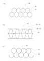
空洞セル10は、狭義では正六角形又は正六角柱を隙間なく並べた構造であるといわれるが、これを広義にとらえて正六柱のみならず、三次元的な充填空間を成す立体も含み、断面視において他の正多角形や円形等も含み、更には繰り返し連続して配置される同一形状を含むものである。
The
不燃紙20は、水酸化アルミニウムを配合した紙に樹脂含侵を施して製造される紙であり、実験的に実施した例では、新日本フェザーコア株式会社(埼玉県さいたま市岩槻区古ケ場1−3−9)から提供されるロールコアーSF(商品名)を用いた。係るロールコア−SFが基材とする水酸化アルミニウムは熱により水を発生する自己消化性があるため、燃えにくく建築材料としても利用されているものである。
The
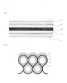
基材30は、不燃紙20を略円柱状の筒に連続成形している形状のコア材であり、厚さ方向における強度差が少ないのが特徴である。但し本発明では、ピラミット形状に成形する為、係る特徴の利点を利用するものではないが、基材としての強度は高い。
The
平板31は、基材30をコルゲートハニカム構造体とする場合に、空洞セル10の形状を成すように、波状板32を両側から挟持して基材30を構成する基材30の一部となる部材である。
When the
波状板32は、基材30をコルゲートハニカム構造体とする場合に、空洞セル10の形状を成すように、平行に配置される前記平板31に挟持され、同一形状が連続して配置される基材の一部である。図2(b)では、波型形状を示したが、これに限定されるものではなく台形や三角形等、同一の形状を繰り返し連続するものであればよい。
When the
導電材料40は、基材30となる不燃紙に導電性を付与するために加える粉体又は繊維等であり、大別するとカーボン系、金属系、金属酸化物系、金属皮膜系、金属酸化物皮膜系などの種類があり、請求項2では、このうち鱗片状のグラファイトを用いることを特定している。係る鱗片状のグラファイトは、熱衝撃にも強く高温になるほど強度が増し、熱膨張率が小さいため、高温での寸法安定性に優れ、急激な大電力による負荷が加わった場合でもその影響を基材30等に与えることなく、電波吸収特性を良好に保ちつつ熱影響の劣化による破損等を防ぐことができる。但し、強固なイオン結合をしているセラミックスや、すべての炭素が共有結合している結晶のダイヤモンドのような素材とは異なり、ファンデルワールス力で結合している鱗片状のグラファイトは壊れやすいため、バインダー80が必要であり、また、導電材料40への酸素供給の遮断及び強度向上の点から、コーティング剤60を用いることが好適である。なお、鱗片状のグラファイトは、塊状のグラファイトと比較して安価なため、コストパフォーマンスに優れるという特徴を有する。
The
コーティング剤60は、不燃紙20からなる基材30に固着された導電材料層50の表面を覆うようにコートして、導電材料40への酸素供給を遮断するための無機化合物によるオーバーコート層70を形成するための被膜剤である。
The coating agent 60 is coated so as to cover the surface of the
バインダー80は、導電材料40を固着させるための接着剤であり、95%以上を無機化合物とし、有機物を5%未満までとし、極力有機物を排除して難燃性を向上させた材料を用いる。
The binder 80 is an adhesive for fixing the
図2は、本発明に係る耐電力電波吸収体に用いられるコア材の断面視における形状実施例を示す実施例説明図であり、図2(a)は、断面視における空洞セルの形状が正六角形である場合を示し、図2(b)は、断面視における空洞セルの形状が平行する二本の直線状の間に連続する波型形状のコルゲート状である場合を示し、図2(c)は、断面視における空洞セルの形状が平行する二本の直線状の間に涙型、及び逆涙型形状が連続するコルゲート涙型ハニカム状である場合を示している。 FIG. 2 is an explanatory view of an example showing a shape embodiment in a cross-sectional view of the core material used for the power-resistant radio wave absorber according to the present invention, and FIG. FIG. 2 (b) shows a case of a square shape, and FIG. 2 (b) shows a case where the shape of the hollow cell in a cross-sectional view is a corrugated shape continuous between two parallel straight lines, and is shown in FIG. 2 (c). ) Indicates a case where the shape of the hollow cell in the cross-sectional view is a corrugated tear-shaped honeycomb in which a tear-shaped shape and a reverse tear-shaped shape are continuous between two parallel straight lines.
図2(a)に示す正六角形状では、隙間を開けることなく力を分散する方向が等角等方に均等に作用するため、同じ正多角形である正三角形や正四角形に比べて、正六角形が最も強度と製作のしやすさ等の観点において優れている。即ち、例えば電波暗室の壁等に設置した場合に、人の接触による耐強度に優れるという効果を発揮するものである。 In the regular hexagonal shape shown in FIG. 2 (a), the direction in which the force is distributed acts evenly at equal angles without leaving a gap. The square shape is the best in terms of strength and ease of manufacture. That is, for example, when it is installed on the wall of an anechoic chamber or the like, it exhibits the effect of being excellent in strength due to human contact.
図3は、本発明に係る耐電力電波吸収体の積層状態を示す状態説明図である。なお、図3は、不燃紙20からなる基材30の表面に導電材料40からなる導電材料層50が固着され、更にその表面に無機化合物からなるコーティング剤60からなるオーバーコート層70が形成されていることを示すものである。
FIG. 3 is a state explanatory view showing a laminated state of the power-resistant radio wave absorber according to the present invention. In FIG. 3, a
導電材料層50は、導電材料40を、極力有機物を排除した(導電材料40及び該導電材料40を固着させるバインダー80が95%以上を無機化合物としたもの)バインダー80で混抄し、ピラミッド型に形成された不燃紙20に固着させた層である。図3に示す通り、導電材料層50は空洞セル10の内側のみならずセル同士の隙間にも成形されるものである。係る導電材料層50の存在により電波を熱に変換して放熱させる層である。本発明では、1.5W/平方センチメートルの電力照射に耐え、1GHzから18GHz帯の電波を良好に吸収する。
The
オーバーコート層70は、不燃紙20に固着された導電材料層50の表面を覆うようにコーティング剤60を塗布して得られる皮膜層である。係るオーバーコート層と、前記導電材料層50の積層状態については図3に示す。係るオーバーコート層70は空洞セル10の内側のみならずセル同士の隙間にも成形されるのは導電材料層50と同様である。
The
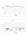
図4は、本発明に係る耐電力電波吸収体と従来品との電波減衰量の対比説明図であり、図4(a)は、従来の電波吸収体(高さ45cmの中空セラミックモール品)の電波減衰量を示し、図4(b)は、本発明に係る耐電力電波吸収体1(同様の外形の中実)の電波減衰量を示しており、本発明に係る耐電力電波吸収体1は0.5GHzから18GHzという広範囲な電波吸収を有するが、図4に示される通り、0.5GHzから4.5GHzのギガヘルツ帯で従来品と比較して特に高い電波吸収性能を示している。 FIG. 4 is a comparative explanatory view of the amount of radio wave attenuation between the power-resistant radio wave absorber according to the present invention and the conventional product, and FIG. 4 (a) is a conventional radio wave absorber (hollow ceramic molding product having a height of 45 cm). 4 (b) shows the radio wave attenuation amount of the power-resistant radio wave absorber 1 (similar outer shape solid) according to the present invention, and shows the radio wave attenuation amount of the power-resistant radio wave absorber according to the present invention. 1 has a wide range of radio wave absorption from 0.5 GHz to 18 GHz, and as shown in FIG. 4, exhibits particularly high radio wave absorption performance in the gigahertz band of 0.5 GHz to 4.5 GHz as compared with the conventional product.
本発明に係る耐電力電波吸収体によれば、大電力密度の電磁波を繰り返し照射しても構造体としての強度や外観等に変化が生じない耐電力性と、電波吸収体としての吸収性能が両立する電波吸収体の提供が出来るため、電波暗室等においての産業上利用可能性は高いと思慮されるものである。
According to the power-resistant radio wave absorber according to the present invention, the power resistance that does not change the strength and appearance of the structure even when repeatedly irradiated with electromagnetic waves having a high power density and the absorption performance as a radio wave absorber are obtained. Since it is possible to provide a compatible radio wave absorber, it is considered that it has high industrial utility in an anechoic chamber or the like.
1 耐電力電波吸収体
10 空洞セル
20 不燃紙
30 基材
31 平板
32 波状板
40 導電材料
50 導電材料層
60 コーティング剤
70 オーバーコート層
80 バインダー
1 Power-resistant
Claims (5)
空洞セル(10)を多数有する不燃紙(20)からなる基材(30)と、
前記基材(30)の表面に固着される無機の導電材料(40)からなる導電材料層(50)と、
更に前記導電材料層(50)の表面に無機化合物のコーティング剤(60)でコートされるオーバーコート層(70)からなり、
前記導電材料(40)及び該導電材料(40)を固着させるバインダー(80)は95%以上が無機化合物であることを特徴とする耐電力電波吸収体(1)。 It is a pyramid-shaped radio wave absorber with excellent heat resistance that can handle high-power irradiation.
A base material (30) made of non-combustible paper (20) having a large number of hollow cells (10),
A conductive material layer (50) made of an inorganic conductive material (40) fixed to the surface of the base material (30),
Further, the surface of the conductive material layer (50) is composed of an overcoat layer (70) coated with an inorganic compound coating agent (60).
The power-resistant radio wave absorber (1), wherein the conductive material (40) and the binder (80) for fixing the conductive material (40) are 95% or more of an inorganic compound.
Claim 1 is characterized in that the cross-sectional shape of the honeycomb-shaped hollow cell (10) is a Namida-shaped shape, and a large number of inverted Namida-shaped shapes facing the Namida-shaped shape are continuously arranged. Alternatively, the withstand power radio wave absorber (1) according to claim 2.
Priority Applications (1)
| Application Number | Priority Date | Filing Date | Title |
|---|---|---|---|
| JP2020073787A JP2021170614A (en) | 2020-04-17 | 2020-04-17 | Power-resistant radio wave absorber |
Applications Claiming Priority (1)
| Application Number | Priority Date | Filing Date | Title |
|---|---|---|---|
| JP2020073787A JP2021170614A (en) | 2020-04-17 | 2020-04-17 | Power-resistant radio wave absorber |
Publications (1)
| Publication Number | Publication Date |
|---|---|
| JP2021170614A true JP2021170614A (en) | 2021-10-28 |
Family
ID=78119435
Family Applications (1)
| Application Number | Title | Priority Date | Filing Date |
|---|---|---|---|
| JP2020073787A Pending JP2021170614A (en) | 2020-04-17 | 2020-04-17 | Power-resistant radio wave absorber |
Country Status (1)
| Country | Link |
|---|---|
| JP (1) | JP2021170614A (en) |
-
2020
- 2020-04-17 JP JP2020073787A patent/JP2021170614A/en active Pending
Similar Documents
| Publication | Publication Date | Title |
|---|---|---|
| JP5496879B2 (en) | Composite wave absorber | |
| JP7074455B2 (en) | Insulation sheet for assembled battery and assembled battery | |
| JP7115906B2 (en) | Heat transfer suppression sheet for assembled battery and assembled battery | |
| CA2432970C (en) | Electromagnetic wave absorber | |
| US10959356B2 (en) | Panel for reflective broadband electromagnetic shielding | |
| JP2004253760A (en) | Sheet material for wave absorber, and wave absorber | |
| CN104582458A (en) | Wave absorbing metamaterial | |
| JP2934048B2 (en) | Foamed phenolic resin composite molding | |
| KR20140007769A (en) | Electromagnetic wave absorber | |
| JP2020072005A (en) | Heat transfer suppressing sheet for assembled battery, sheet structure, and assembled battery | |
| JP2019204637A (en) | Heat transmission suppression sheet for battery pack and battery pack | |
| KR101576070B1 (en) | Multilayer flexible electromagnetic wave absorber | |
| CN211481841U (en) | Heat dissipation absorbing material composite construction | |
| JP2021170614A (en) | Power-resistant radio wave absorber | |
| US20100263187A1 (en) | Exhaust Gas Deflector and Shield | |
| KR101508989B1 (en) | Honeycomb module for fire door | |
| JP2005311332A (en) | Radio wave absorbing sheet and radio wave absorber using the same | |
| JP6168733B2 (en) | Insulation | |
| AU1947601A (en) | Thermal insulating device | |
| JP7445912B2 (en) | radio wave absorber | |
| JP7307217B2 (en) | Heat transfer suppression sheet for assembled battery and assembled battery | |
| CN219773426U (en) | Indoor heating building material | |
| KR20120097909A (en) | Insulating panel for construction | |
| US11046583B2 (en) | Wave-to-heat conversion structure and application thereof | |
| KR102082918B1 (en) | insulator |
Legal Events
| Date | Code | Title | Description |
|---|---|---|---|
| A80 | Written request to apply exceptions to lack of novelty of invention |
Free format text: JAPANESE INTERMEDIATE CODE: A80 Effective date: 20200421 |