JP2021057504A - Light-emitting device - Google Patents

Light-emitting device Download PDF

Info

Publication number
JP2021057504A
JP2021057504A JP2019181023A JP2019181023A JP2021057504A JP 2021057504 A JP2021057504 A JP 2021057504A JP 2019181023 A JP2019181023 A JP 2019181023A JP 2019181023 A JP2019181023 A JP 2019181023A JP 2021057504 A JP2021057504 A JP 2021057504A
Authority
JP
Japan
Prior art keywords
light
substrate
emitting device
light emitting
opening
Prior art date
Legal status (The legal status is an assumption and is not a legal conclusion. Google has not performed a legal analysis and makes no representation as to the accuracy of the status listed.)
Granted
Application number
JP2019181023A
Other languages
Japanese (ja)
Other versions
JP7144682B2 (en
Inventor
功喜 芝井
Koki Shibai
功喜 芝井
Current Assignee (The listed assignees may be inaccurate. Google has not performed a legal analysis and makes no representation or warranty as to the accuracy of the list.)
Nichia Chemical Industries Ltd
Original Assignee
Nichia Chemical Industries Ltd
Priority date (The priority date is an assumption and is not a legal conclusion. Google has not performed a legal analysis and makes no representation as to the accuracy of the date listed.)
Filing date
Publication date
Application filed by Nichia Chemical Industries Ltd filed Critical Nichia Chemical Industries Ltd
Priority to JP2019181023A priority Critical patent/JP7144682B2/en
Priority to US17/033,400 priority patent/US11437429B2/en
Publication of JP2021057504A publication Critical patent/JP2021057504A/en
Priority to US17/876,521 priority patent/US11798977B2/en
Application granted granted Critical
Publication of JP7144682B2 publication Critical patent/JP7144682B2/en
Active legal-status Critical Current
Anticipated expiration legal-status Critical

Links

Images

Abstract

To fix a light-reflecting member to a substrate by a resin member.SOLUTION: A light-emitting device includes a substrate, a plurality of light sources arranged on the substrate, and a light-reflecting member arranged on the substrate and having a wall portion surrounding the plurality of light sources one by one or two or more of them; the wall portion has a cavity portion having a first opening on the substrate side; the substrate has a penetrating hole that penetrates the substrate in the vertical direction and has a second opening located inside the first opening on the upper surface of the substrate; and a resin member is continuously in contact with the inner wall of the cavity portion and a region on the upper surface of the substrate provided between the peripheral edge of the second opening and the peripheral edge of the first opening.SELECTED DRAWING: Figure 1E

Description

本発明は発光装置に関する。 The present invention relates to a light emitting device.

複数の光源と、これら光源を囲む壁部を備えた反射部材とを、基板上に配置するバックライト装置が提案されている(特許文献1の段落0032参照)。 A backlight device has been proposed in which a plurality of light sources and a reflecting member provided with a wall portion surrounding the light sources are arranged on a substrate (see paragraph 0032 of Patent Document 1).

国際公開第2012/023459号International Publication No. 2012/023459

光取り出し効率に優れた発光装置が望まれる。 A light emitting device having excellent light extraction efficiency is desired.

本発明は次の一実施形態を含む。 The present invention includes the following embodiment.

基板と、
前記基板上に配置される複数の光源と、
前記基板上に配置され、前記複数の光源を1つずつまたは2つ以上ずつ囲む壁部を備えた光反射性部材と、を備えた発光装置であって、
前記壁部は、前記基板側に第1開口を有する空洞部を有し、
前記基板は、前記基板を上下方向に貫通し、前記第1開口の内側に位置する第2開口を前記基板の上面に有する貫通孔を有し、
前記空洞部の内壁と、前記第2開口の周縁と前記第1開口の周縁との間に設けられる前記基板上面の領域と、に樹脂部材が連続して接している発光装置。
With the board
With a plurality of light sources arranged on the substrate,
A light emitting device including a light-reflecting member arranged on the substrate and having a wall portion surrounding the plurality of light sources one by one or two or more.
The wall portion has a hollow portion having a first opening on the substrate side.
The substrate has a through hole that penetrates the substrate in the vertical direction and has a second opening located inside the first opening on the upper surface of the substrate.
A light emitting device in which a resin member is continuously in contact with an inner wall of the cavity and a region on the upper surface of the substrate provided between the peripheral edge of the second opening and the peripheral edge of the first opening.

本発明の一実施形態によれば、光取り出し効率に優れた発光装置が得られる。 According to one embodiment of the present invention, a light emitting device having excellent light extraction efficiency can be obtained.

実施形態1に係る発光装置の模式的平面図である。It is a schematic plan view of the light emitting device which concerns on Embodiment 1. FIG. 図1Aにおいて壁部の側面部にハッチングを施した図である。FIG. 1A is a view in which a side surface portion of a wall portion is hatched. 図1Aにおいて壁部の底面部にハッチングを施した図である。FIG. 1A is a view in which the bottom surface of the wall portion is hatched. 基板の貫通孔(第2開口)と光源との位置関係を示す図である。It is a figure which shows the positional relationship between the through hole (second opening) of a substrate, and a light source. 図1A中の1E−1E断面を示す図である。It is a figure which shows the cross section of 1E-1E in FIG. 1A. 実施形態2に係る発光装置の模式的平面図である。It is a schematic plan view of the light emitting device which concerns on Embodiment 2. FIG. 図2Aにおいて壁部の先端部にハッチングを施した図である。FIG. 2A is a view in which the tip portion of the wall portion is hatched. 図2Aにおいて壁部の側面部にハッチングを施した図である。FIG. 2A is a view in which the side surface portion of the wall portion is hatched. 図2Aにおいて壁部の底面部にハッチングを施した図である。FIG. 2A is a view in which the bottom surface of the wall portion is hatched. 基板の貫通孔(第2開口)と光源との位置関係を示す図である。It is a figure which shows the positional relationship between the through hole (second opening) of a substrate, and a light source. 図2A中の2F−2F断面を示す図である。It is a figure which shows the 2F-2F cross section in FIG. 2A. 実施形態1に係る発光装置の製造方法を説明する模式的断面図である。It is a schematic cross-sectional view explaining the manufacturing method of the light emitting device which concerns on Embodiment 1. FIG. 実施形態1に係る発光装置の製造方法を説明する模式的断面図である。It is a schematic cross-sectional view explaining the manufacturing method of the light emitting device which concerns on Embodiment 1. FIG. 実施形態1に係る発光装置の製造方法を説明する模式的断面図である。It is a schematic cross-sectional view explaining the manufacturing method of the light emitting device which concerns on Embodiment 1. FIG. 実施形態1に係る発光装置の製造方法を説明する模式的断面図である。It is a schematic cross-sectional view explaining the manufacturing method of the light emitting device which concerns on Embodiment 1. FIG. 実施形態2に係る発光装置の製造方法を説明する模式的断面図である。It is a schematic cross-sectional view explaining the manufacturing method of the light emitting device which concerns on Embodiment 2. FIG. 実施形態2に係る発光装置の製造方法を説明する模式的断面図である。It is a schematic cross-sectional view explaining the manufacturing method of the light emitting device which concerns on Embodiment 2. FIG. 実施形態2に係る発光装置の製造方法を説明する模式的断面図である。It is a schematic cross-sectional view explaining the manufacturing method of the light emitting device which concerns on Embodiment 2. FIG. 実施形態2に係る発光装置の製造方法を説明する模式的断面図である。It is a schematic cross-sectional view explaining the manufacturing method of the light emitting device which concerns on Embodiment 2. FIG. 壁部の先端部が、発光装置の上方に配置される部材に接する場合(実施形態2の場合)において、1つのセルを光源を点灯させながら平面視した場合の一例を示す写真である。It is a photograph which shows an example of the case where one cell is viewed in a plan view while lighting a light source when the tip end portion of a wall portion is in contact with a member arranged above the light emitting device (in the case of the second embodiment). 壁部の先端部が、発光装置の上方に配置される部材に接しない場合(比較例の場合)において、1つのセルを光源を点灯させながら平面視した場合の一例を示す写真である。It is a photograph which shows an example of the case where one cell is viewed in a plan view while lighting a light source when the tip end portion of a wall portion does not come into contact with a member arranged above the light emitting device (in the case of a comparative example).

以下、図面を参照しながら、本開示の発光装置を詳細に説明する。本開示の発光装置は例示であり、以下で説明する発光装置に限られない。以下の説明では、特定の方向や位置を示す用語(例えば、「上」、「下」およびそれらの用語を含む別の用語)を用いる場合がある。それらの用語は、参照した図面における相対的な方向や位置を、分かり易さのために用いているに過ぎない。また、図面が示す構成要素の大きさや位置関係等は、分かり易さのため、誇張されている場合があり、実際の発光装置における大きさ、あるいは実際の発光装置における構成要素間の大小関係を反映していない場合がある。また、理解を容易にするため、各部材の図示を適宜省略することがある。 Hereinafter, the light emitting device of the present disclosure will be described in detail with reference to the drawings. The light emitting device of the present disclosure is an example, and is not limited to the light emitting device described below. In the following description, terms indicating a specific direction or position (for example, "top", "bottom" and other terms including those terms) may be used. These terms use relative orientation and position in the referenced drawings for clarity only. In addition, the size and positional relationship of the components shown in the drawings may be exaggerated for the sake of clarity, and the size in the actual light emitting device or the size relationship between the components in the actual light emitting device may be exaggerated. It may not be reflected. Further, in order to facilitate understanding, the illustration of each member may be omitted as appropriate.

[実施形態1に係る発光装置1]
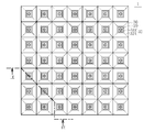
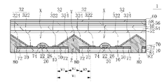
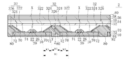
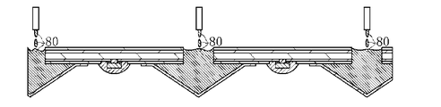
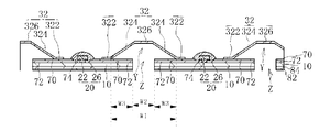
図1Aは実施形態1に係る発光装置の模式的平面図である。図1Bは、図1Aにおいて壁部32の側面部324にハッチングを施した図である。図1Cは、図1Aにおいて壁部32の底面部322にハッチングを施した図である。図1Dは、基板の貫通孔(第2開口)と光源との位置関係を示す図である。図1Dにおいては、光反射性部材30と接着剤80の図示を省略している。図1Eは図1A中の1E−1E断面を示す図である。図1Eにおいては、発光装置1の上方に配置される部材もあわせて図示している。
[Light emitting device 1 according to the first embodiment]
FIG. 1A is a schematic plan view of the light emitting device according to the first embodiment. FIG. 1B is a view in which the side surface portion 324 of the wall portion 32 is hatched in FIG. 1A. FIG. 1C is a view in which the bottom surface portion 322 of the wall portion 32 is hatched in FIG. 1A. FIG. 1D is a diagram showing the positional relationship between the through hole (second opening) of the substrate and the light source. In FIG. 1D, the light reflecting member 30 and the adhesive 80 are not shown. FIG. 1E is a diagram showing a cross section of 1E-1E in FIG. 1A. In FIG. 1E, a member arranged above the light emitting device 1 is also shown.

図1A乃至図1Eに示すように、実施形態1に係る発光装置1は、基板10と、基板10上に配置される複数の光源20と、基板10上に配置され、複数の光源20を1つずつまたは2つ以上ずつ囲む壁部32を備えた光反射性部材30と、を備えた発光装置であって、壁部32は、基板10側に第1開口W1を有する空洞部Yを有し、基板10は、基板10を上下方向に貫通し、第1開口W1の内側に位置する第2開口W2を基板10の上面に有する貫通孔Zを有し、空洞部Yの内壁と、第2開口W2の周縁と第1開口W1の周縁との間に設けられる基板10上面の領域W3と、に樹脂部材80が連続して接している発光装置である。以下、詳細に説明する。 As shown in FIGS. 1A to 1E, the light emitting device 1 according to the first embodiment includes a substrate 10, a plurality of light sources 20 arranged on the substrate 10, and a plurality of light sources 20 arranged on the substrate 10. A light source including a light-reflecting member 30 having wall portions 32 surrounding one by one or two or more, and the wall portion 32 has a cavity portion Y having a first opening W1 on the substrate 10 side. The substrate 10 has a through hole Z that penetrates the substrate 10 in the vertical direction and has a second opening W2 located inside the first opening W1 on the upper surface of the substrate 10. This is a light emitting device in which the resin member 80 is continuously in contact with the region W3 on the upper surface of the substrate 10 provided between the peripheral edge of the two openings W2 and the peripheral edge of the first opening W1. Hereinafter, a detailed description will be given.

(基板10)
基板10は、複数の光源20を配置するための部材である。
(Board 10)
The substrate 10 is a member for arranging a plurality of light sources 20.

基板10は、例えば、ロール・ツー・ロール方式で製造可能なフレキシブル基板であってもよいし、リジット基板であってもよい。リジット基板は湾曲可能な薄型リジット基板であってもよい。 The substrate 10 may be, for example, a flexible substrate that can be manufactured by a roll-to-roll method, or a rigid substrate. The rigid substrate may be a curvable thin rigid substrate.

基板10の材料としては、例えば、セラミックス、フェノール樹脂、エポキシ樹脂、ポリイミド樹脂、BTレジン、ポリフタルアミド(PPA)、ポリエチレンテレフタレート(PET)等の樹脂が挙げられる。セラミックスとしては、例えば、アルミナ、ムライト、フォルステライト、ガラスセラミックス、窒化物系(例えば、AlN)、炭化物系(例えば、SiC)、LTCC等である。樹脂を用いる場合は、ガラス繊維や、SiO、TiO、Al等の無機フィラーを樹脂に混合し、機械的強度の向上、熱膨張率の低減、光反射率の向上等を図ることもできる。金属部材の表面に絶縁層が形成された金属基板を用いてもよい。 Examples of the material of the substrate 10 include resins such as ceramics, phenol resin, epoxy resin, polyimide resin, BT resin, polyphthalamide (PPA), and polyethylene terephthalate (PET). Examples of the ceramics include alumina, mullite, forsterite, glass ceramics, nitride-based (for example, AlN), carbide-based (for example, SiC), and LTCC. When using a resin, glass fiber or an inorganic filler such as SiO 2 , TiO 2 , Al 2 O 3 is mixed with the resin to improve mechanical strength, reduce the coefficient of thermal expansion, improve the light reflectance, etc. You can also do it. A metal substrate having an insulating layer formed on the surface of the metal member may be used.

基板10の厚さは適宜選択することができる。 The thickness of the substrate 10 can be appropriately selected.

基板10の上面は、光反射性部材30を配置しやすいよう、平面であることが好ましい。平面には平面であるとみなせる場合を含む。基板10の平面視形状には、正方形、長方形、または円形などが含まれる。これら正方形、長方形、または円形には、正方形とみなせる場合、長方形とみなせる場合、または円形とみなせる場合が含まれる。 The upper surface of the substrate 10 is preferably flat so that the light reflecting member 30 can be easily arranged. The plane includes the case where it can be regarded as a plane. The plan view shape of the substrate 10 includes a square, a rectangle, a circle, and the like. These squares, rectangles, or circles include cases that can be regarded as squares, rectangles, or circles.

基板10は、基板10を上下方向に貫通する貫通孔Zを有している。これにより、基板10の下面側からこの貫通孔Zを介して、光反射性部材30の壁部32が有する空洞部Y内に樹脂部材80を注入することが可能となる。貫通孔Zは、第2開口W2を基板10の上面に有しており、この第2開口W2を通じて、光反射性部材30の壁部32が有する空洞部Yに繋がっている。貫通孔Zの内径や形状等は、樹脂部材80を空洞部Yに注入可能である限り、限定されない。ただし、第2開口W2(第2開口W2の外縁)は第1開口W1(第1開口W1の外縁)の内側に位置する。これにより、第2開口W2の周縁と第1開口W1の周縁との間に基板10上面の領域W3が確保され、当該領域W3と空洞部Yの内壁とに樹脂部材80が連続して接することが可能となる。例えば、基板10の厚みが0.5mmであり、第1開口W1の直径が3mmであるとすると、第2開口W2の直径は1mmである。この場合、第2開口W2の周縁と第1開口W1の周縁との間に形成される基板10上面の領域W3は、断面視における第2開口W2の右側と左側とにそれぞれ設けられ、その長さはともに1mmである。つまり、例えば、断面視において、(第2開口W2の周縁と第1開口W1の周縁との間に形成される基板10上面の領域W3の長さ)+第2開口W2の直径+(第2開口W2の周縁と第1開口W1の周縁との間に形成される基板10上面の領域W3の長さ)=第1開口W1の直径となる。 The substrate 10 has a through hole Z that penetrates the substrate 10 in the vertical direction. As a result, the resin member 80 can be injected into the cavity Y of the wall portion 32 of the light reflecting member 30 from the lower surface side of the substrate 10 through the through hole Z. The through hole Z has a second opening W2 on the upper surface of the substrate 10, and is connected to the hollow portion Y of the wall portion 32 of the light reflecting member 30 through the second opening W2. The inner diameter and shape of the through hole Z are not limited as long as the resin member 80 can be injected into the cavity Y. However, the second opening W2 (outer edge of the second opening W2) is located inside the first opening W1 (outer edge of the first opening W1). As a result, the region W3 on the upper surface of the substrate 10 is secured between the peripheral edge of the second opening W2 and the peripheral edge of the first opening W1, and the resin member 80 is continuously in contact with the region W3 and the inner wall of the cavity portion Y. Is possible. For example, assuming that the thickness of the substrate 10 is 0.5 mm and the diameter of the first opening W1 is 3 mm, the diameter of the second opening W2 is 1 mm. In this case, the regions W3 on the upper surface of the substrate 10 formed between the peripheral edge of the second opening W2 and the peripheral edge of the first opening W1 are provided on the right side and the left side of the second opening W2 in the cross-sectional view, respectively, and their lengths thereof. Both are 1 mm. That is, for example, in a cross-sectional view, (the length of the region W3 on the upper surface of the substrate 10 formed between the peripheral edge of the second opening W2 and the peripheral edge of the first opening W1) + the diameter of the second opening W2 + (the second). The length of the region W3 on the upper surface of the substrate 10 formed between the peripheral edge of the opening W2 and the peripheral edge of the first opening W1) = the diameter of the first opening W1.

貫通孔Zの数は1つであってもよいが、壁部32の空洞部Y内に樹脂部材80を効率的に注入できるよう、複数であることが好ましい。 The number of through holes Z may be one, but it is preferable that the number of through holes Z is a plurality so that the resin member 80 can be efficiently injected into the cavity Y of the wall portion 32.

(複数の光源20)
複数の光源20は、基板10上に配置される。具体的に説明すると、複数の光源20は、発光装置1を平面視した場合において、光反射性部材30が存在しない領域に配置され、実装される。当該領域には後述する導電部材72が露出しており、当該導電部材72に光源20の電極が電気的に接続される。なお、当該領域は、開口部などと呼ぶことができる。光源20は、例えば、フリップチップ方式により実装することができるが、ワイヤを用いたワイヤボンディング等、その他の方法により実装することもできる。
(Multiple light sources 20)
The plurality of light sources 20 are arranged on the substrate 10. Specifically, the plurality of light sources 20 are arranged and mounted in a region where the light reflecting member 30 does not exist when the light emitting device 1 is viewed in a plan view. A conductive member 72, which will be described later, is exposed in the region, and the electrode of the light source 20 is electrically connected to the conductive member 72. The area can be called an opening or the like. The light source 20 can be mounted by, for example, a flip chip method, but can also be mounted by other methods such as wire bonding using wires.

複数の光源20間の間隔、つまり複数の光源20が隣接する間隔は、例えば5mm以上25mm以下であるが、平面視における縦方向及び横方向において均一(均一であるとみなせる場合を含む。)であることが好ましい。 The distance between the plurality of light sources 20, that is, the distance between the plurality of light sources 20 adjacent to each other is, for example, 5 mm or more and 25 mm or less, but is uniform (including the case where it can be regarded as uniform) in the vertical and horizontal directions in a plan view. It is preferable to have.

複数の光源20は、互いに独立して駆動可能であることが好ましく、特に、光源20ごとの調光制御(例えば、ローカルディミングやハイダイナミックレンジ:HDR)が可能であることが好ましい。 It is preferable that the plurality of light sources 20 can be driven independently of each other, and in particular, it is preferable that dimming control for each light source 20 (for example, local dimming or high dynamic range: HDR) is possible.

複数の光源20それぞれは、例えば青色の光を発する。ただし、青色のほか、黄色、緑色、または赤色であってもよい。 Each of the plurality of light sources 20 emits blue light, for example. However, in addition to blue, it may be yellow, green, or red.

各光源20は発光ダイオードなどの発光素子22を有していてもよい。発光素子22は、例えば、透光性の基板と、基板上に積層された半導体層と、を有する。透光性の基板には、例えばサファイアを用いることができる。半導体層は、例えば、n型半導体層、活性層、及びP型半導体層を、基板側からこの順に有している。半導体層には、例えば、ZnSe、窒化物系半導体(InAlGa1−x−yN、0≦X、0≦Y、X+Y≦1)、またはGaPなどのほか、GaAlAs、AlInGaPなどを用いることができる。n型半導体層には例えばn側電極が接続されており、P型半導体層には例えばP側電極が接続されている。各光源20は、発光素子22の上面(発光素子が配置される基板に近い面と反対側の面)に反射層を有していてもよい。反射層は、金属膜であってもよいし、誘電体多層膜であってもよい。 Each light source 20 may have a light emitting element 22 such as a light emitting diode. The light emitting element 22 has, for example, a translucent substrate and a semiconductor layer laminated on the substrate. For the translucent substrate, for example, sapphire can be used. The semiconductor layer has, for example, an n-type semiconductor layer, an active layer, and a P-type semiconductor layer in this order from the substrate side. Examples of the semiconductor layer include ZnSe, nitride-based semiconductors (In x Al y Ga 1-x-y N, 0 ≦ X, 0 ≦ Y, X + Y ≦ 1), GaP, and the like, as well as GaAlAs and AlInGaP. Can be used. For example, an n-side electrode is connected to the n-type semiconductor layer, and for example, a P-side electrode is connected to the P-type semiconductor layer. Each light source 20 may have a reflective layer on the upper surface of the light emitting element 22 (the surface opposite to the surface close to the substrate on which the light emitting element is arranged). The reflective layer may be a metal film or a dielectric multilayer film.

各光源20は封止部材26を有していてもよい。封止部材26は、発光素子22を外部環境から保護するとともに、発光素子22から出力される光を光学的に制御する部材である。封止部材26は、発光素子22を被覆するように基板10上に配置される。封止部材26の材料としては、エポキシ樹脂やシリコーン樹脂あるいはそれらを混合させた樹脂や、ガラスなどの透光性材料を用いることができる。これらのうち、耐光性および成形のしやすさを考慮して、シリコーン樹脂を選択することが好ましい。封止部材26には、光拡散材や、発光素子22からの光を吸収して発光素子22からの出力光とは異なる波長の光を発する蛍光体等の波長変換材や、発光素子22の発光色に対応する着色剤を含有させることができる。封止部材26は、例えば、圧縮成型や射出成型などのほか、滴下や描画により形成することができる。また、封止部材26の材料の粘度を最適化することにより、材料自体の表面張力によって形状を制御することも可能である。滴下や描画による場合は、金型を必要とすることなく、より簡便に封止部材26を形成することができる。粘度は、所望の粘度を有する材料を封止部材26の材料として用いることにより調整してもよいし、上述した光拡散材、波長変換材、あるいは着色剤を利用して調整してもよい。 Each light source 20 may have a sealing member 26. The sealing member 26 is a member that protects the light emitting element 22 from the external environment and optically controls the light output from the light emitting element 22. The sealing member 26 is arranged on the substrate 10 so as to cover the light emitting element 22. As the material of the sealing member 26, an epoxy resin, a silicone resin, a resin in which they are mixed, or a translucent material such as glass can be used. Of these, it is preferable to select a silicone resin in consideration of light resistance and ease of molding. The sealing member 26 includes a light diffusing material, a wavelength conversion material such as a phosphor that absorbs light from the light emitting element 22 and emits light having a wavelength different from the output light from the light emitting element 22, and the light emitting element 22. A colorant corresponding to the emission color can be contained. The sealing member 26 can be formed by, for example, compression molding or injection molding, as well as dropping or drawing. Further, by optimizing the viscosity of the material of the sealing member 26, it is possible to control the shape by the surface tension of the material itself. In the case of dropping or drawing, the sealing member 26 can be formed more easily without the need for a mold. The viscosity may be adjusted by using a material having a desired viscosity as the material of the sealing member 26, or may be adjusted by using the above-mentioned light diffusing material, wavelength converting material, or colorant.

各光源20はバットウィング型の配光特性を有していることが好ましい。このようにすれば、各光源20の真上方向に出射される光量を抑制して、各光源20の配光を広げることができる。したがって、特に基板10と対向して透光性の光学部材54を設ける場合において、発光装置1の厚みを小さくすることができる。バットウィング型の配光特性とは、中心部が外周部よりも暗くなる配光特性をいう。バットウィング型の配光特性の一例としては、光軸Lを0°とする場合に、0°よりも配光角の絶対値が大きい角度において、発光強度が強くなる発光強度分布を有する配光特性や、45°〜90°付近において、発光強度が最も強くなる発光強度分布を有する配向特性を挙げることができる。封止部材26は、例えば発光素子22と反射層とを被覆するように設けることができる。このように封止部材26を設ければ、バットウィング型の配光特性を容易に実現することができる。 It is preferable that each light source 20 has a butt wing type light distribution characteristic. In this way, the amount of light emitted in the direction directly above each light source 20 can be suppressed, and the light distribution of each light source 20 can be expanded. Therefore, the thickness of the light emitting device 1 can be reduced, especially when the translucent optical member 54 is provided so as to face the substrate 10. The butt-wing type light distribution characteristic refers to a light distribution characteristic in which the central portion becomes darker than the outer peripheral portion. As an example of the butt-wing type light distribution characteristic, when the optical axis L is 0 °, the light distribution has a light emission intensity distribution in which the light emission intensity becomes stronger at an angle where the absolute value of the light distribution angle is larger than 0 °. Examples thereof include characteristics and orientation characteristics having an emission intensity distribution in which the emission intensity is strongest in the vicinity of 45 ° to 90 °. The sealing member 26 can be provided so as to cover, for example, the light emitting element 22 and the reflective layer. If the sealing member 26 is provided in this way, the butt wing type light distribution characteristic can be easily realized.

(光反射性部材30)
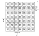
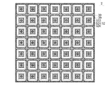
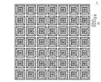
光反射性部材30は、基板10上に配置され、複数の光源20を囲む壁部32を備える部材である。光反射性部材30は、リフレクタと呼ばれることがある。壁部32は、本実施形態のように複数の光源20を1つずつ囲んでもよいし、2つ以上ずつ囲んでもよい。つまり、壁部32は複数の包囲部Xを有しており、各包囲部Xには1つの光源20または2つ以上の光源20が配置される。なお、本明細書では、包囲部Xをセルと呼ぶことがある。
(Light reflective member 30)
The light reflective member 30 is a member that is arranged on the substrate 10 and includes a wall portion 32 that surrounds a plurality of light sources 20. The light reflecting member 30 is sometimes called a reflector. The wall portion 32 may surround a plurality of light sources 20 one by one as in the present embodiment, or may surround two or more light sources 20 at a time. That is, the wall portion 32 has a plurality of surrounding portions X, and one light source 20 or two or more light sources 20 are arranged in each surrounding portion X. In this specification, the surrounding portion X may be referred to as a cell.

壁部32は、基板10側に第1開口W1を有する空洞部Yを有する。この第1開口W1と基板10の第2開口W2が重なりを有することにより、基板10の貫通孔Zと壁部32の空洞部Yが繋がり、基板10の下面側から基板10の貫通孔Zを介して、壁部32の空洞部Y内に樹脂部材80を注入することが可能となる。第1開口W1の内径や形状等は、樹脂部材80を空洞部Yに注入可能である限り、限定されない。ただし、第1開口W1(第1開口W1の外縁)は第2開口W2(第2開口W2の外縁)の外側に位置する。これにより、第2開口W2の周縁と第1開口W1の周縁との間に基板10上面の領域W3が確保され、当該領域W3と空洞部Yの内壁とに樹脂部材80が連続して接することが可能となる。なお、樹脂部材80は、壁部32の空洞部Y内に充満、つまり壁部32の空洞部Y内のすべての空間が樹脂部材80により満たされていてもよい(換言すると、埋め尽くされていてもよい)。ただし、樹脂部材80は、本実施形態のように、平面視において、第2開口W2の周縁から面状(面とみなせる場合を含む)に広がる程度に空洞内に注入されていることが好ましい。換言すると、空洞部Y内のすべての空間を樹脂部材80で満たす必要はなく、樹脂部材80は、光反射性部材30が基板10に必要にして十分に固定される程度において、空洞部Y内に注入されればよい。 The wall portion 32 has a cavity portion Y having a first opening W1 on the substrate 10 side. Since the first opening W1 and the second opening W2 of the substrate 10 overlap each other, the through hole Z of the substrate 10 and the cavity Y of the wall portion 32 are connected, and the through hole Z of the substrate 10 is formed from the lower surface side of the substrate 10. Through this, the resin member 80 can be injected into the hollow portion Y of the wall portion 32. The inner diameter and shape of the first opening W1 are not limited as long as the resin member 80 can be injected into the cavity Y. However, the first opening W1 (outer edge of the first opening W1) is located outside the second opening W2 (outer edge of the second opening W2). As a result, the region W3 on the upper surface of the substrate 10 is secured between the peripheral edge of the second opening W2 and the peripheral edge of the first opening W1, and the resin member 80 is continuously in contact with the region W3 and the inner wall of the cavity portion Y. Is possible. The resin member 80 may be filled in the hollow portion Y of the wall portion 32, that is, all the spaces in the hollow portion Y of the wall portion 32 may be filled with the resin member 80 (in other words, the resin member 80 is completely filled). May be). However, it is preferable that the resin member 80 is injected into the cavity to the extent that it spreads in a planar shape (including a case where it can be regarded as a surface) from the peripheral edge of the second opening W2 in a plan view as in the present embodiment. In other words, it is not necessary to fill all the spaces in the cavity Y with the resin member 80, and the resin member 80 is provided in the cavity Y to the extent that the light reflecting member 30 is required and sufficiently fixed to the substrate 10. It may be injected into.

光反射性部材30は、底面部322を備え、底面部322は基板10上に配置されることが好ましい。これにより、光反射性部材30を基板10上に安定的に配置することができる。底面部322は、より安定的に光反射性部材30を配置することができるよう、平面状であることが好ましい。底面部322と基板10の間には両面テープが介在しない。 It is preferable that the light reflecting member 30 includes a bottom surface portion 322, and the bottom surface portion 322 is arranged on the substrate 10. As a result, the light reflective member 30 can be stably arranged on the substrate 10. The bottom surface portion 322 is preferably flat so that the light reflecting member 30 can be arranged more stably. No double-sided tape is interposed between the bottom surface portion 322 and the substrate 10.

壁部32は、例えば、光反射性部材30が外に向かって開くように屈曲することによってなる。換言すると、壁部32は、例えば、光反射性部材30が上方に向かって凸となるように屈曲することによってなる。光反射性部材30は、例えば、底面部322と、このような壁部32と、が繰り返される形状を有している。壁部32の空洞部Yは、例えば、光反射性部材30が屈曲することによって光反射性部材30の下側に形成される凹みである。空洞部Yの第1開口W1は、そのような凹みの開口面であり、例えば、底面部322の下面と同一の平面にある。つまり、第1開口W1の開口面と、底面部322の下面とは、基板10の上面を基準にした高さが同じである。 The wall portion 32 is formed by, for example, bending the light reflecting member 30 so as to open outward. In other words, the wall portion 32 is formed by, for example, bending the light reflecting member 30 so as to be convex upward. The light-reflecting member 30 has a shape in which, for example, a bottom surface portion 322 and such a wall portion 32 are repeated. The hollow portion Y of the wall portion 32 is, for example, a recess formed on the lower side of the light reflecting member 30 by bending the light reflecting member 30. The first opening W1 of the cavity portion Y is an opening surface of such a recess, and is, for example, on the same plane as the lower surface of the bottom surface portion 322. That is, the opening surface of the first opening W1 and the lower surface of the bottom surface portion 322 have the same height with respect to the upper surface of the substrate 10.

壁部32の側面は、光源20からの光が上方に向けて反射されやすいよう、壁部32の先端部326が、底面部322よりも光源20から離れるように傾斜する側面部324を有していることが好ましい。光源20からの光が上方に向けて反射されやすいよう、側面部324は、傾斜平面を有している、あるいは側面部324のすべてが傾斜平面からなることが好ましい。側面部324の一端から底面部322が延伸し、他端から壁部32の先端部326が延伸する。 The side surface of the wall portion 32 has a side surface portion 324 in which the tip portion 326 of the wall portion 32 is inclined so as to be farther from the light source 20 than the bottom surface portion 322 so that the light from the light source 20 is easily reflected upward. Is preferable. It is preferable that the side surface portion 324 has an inclined plane, or all of the side surface portions 324 are formed of the inclined plane so that the light from the light source 20 is easily reflected upward. The bottom surface portion 322 extends from one end of the side surface portion 324, and the tip portion 326 of the wall portion 32 extends from the other end.

壁部32間の間隔、つまり壁部32が隣接する間隔は、例えば5mm以上25以下であるが、平面視における縦方向及び横方向において均一(均一であるとみなせる場合を含む。)であることが好ましい。 The distance between the wall portions 32, that is, the distance between the wall portions 32 adjacent to each other is, for example, 5 mm or more and 25 or less, but is uniform (including the case where it can be regarded as uniform) in the vertical direction and the horizontal direction in a plan view. Is preferable.

光反射性部材30には、例えば、酸化チタン、酸化アルミニウム、酸化ケイ素等の金属酸化物粒子からなる反射材を含有する樹脂を用いて成形された部材や、反射材を含有しない樹脂の表面に反射材が設けられた部材などを用いることができる。 The light-reflecting member 30 may be formed on a member formed by using a resin containing a reflective material made of metal oxide particles such as titanium oxide, aluminum oxide, or silicon oxide, or on the surface of a resin containing no reflective material. A member provided with a reflective material or the like can be used.

光反射性部材30の厚み(基板10の上面から壁部32の上端までの高さ)は、例えば100〜300μmである。光反射性部材30の厚みは均一であることが好ましい。均一には、均一であるとみなせる場合を含む。 The thickness of the light reflecting member 30 (height from the upper surface of the substrate 10 to the upper end of the wall portion 32) is, for example, 100 to 300 μm. The thickness of the light reflecting member 30 is preferably uniform. Uniformity includes the case where it can be regarded as uniform.

(樹脂部材80)
樹脂部材80は、空洞部Yの内壁と、第2開口W2の周縁と第1開口W1の周縁との間に設けられる基板10上面の領域W3と、に連続して接している。このように、樹脂部材80が、空洞部Yの内壁と基板10上面の領域W3とを互いに接着することにより、光反射性部材30を基板10に固定することが可能となる。なお、樹脂部材80は、光反射性部材30の熱収縮による位置ズレを抑制するアンカーとしての役割を果たすこともできる。
(Resin member 80)
The resin member 80 is continuously in contact with the inner wall of the cavity Y and the region W3 on the upper surface of the substrate 10 provided between the peripheral edge of the second opening W2 and the peripheral edge of the first opening W1. In this way, the resin member 80 can fix the light reflective member 30 to the substrate 10 by adhering the inner wall of the cavity Y and the region W3 on the upper surface of the substrate 10 to each other. The resin member 80 can also serve as an anchor that suppresses the positional deviation due to heat shrinkage of the light reflecting member 30.

樹脂部材80は、光源20から出射された光を反射する部材とすることができる。このようにすれば、光反射性部材30の反射率を向上させることができる。他方、樹脂部材80は、光源20から出射された光を吸収する部材とすることもできる。このようにすれば、ローカルディミング時に隣接する非点灯セルへの漏れ光を削減することができる。 The resin member 80 can be a member that reflects the light emitted from the light source 20. In this way, the reflectance of the light reflective member 30 can be improved. On the other hand, the resin member 80 can also be a member that absorbs the light emitted from the light source 20. In this way, it is possible to reduce the light leakage to the adjacent non-lighting cell during local dimming.

樹脂部材80には例えば熱可塑性樹脂などを用いることができる。 For the resin member 80, for example, a thermoplastic resin or the like can be used.

以上説明した実施形態1に係る発光装置1によれば、光取り出し効率に優れた発光装置が得られる。 According to the light emitting device 1 according to the first embodiment described above, a light emitting device having excellent light extraction efficiency can be obtained.

光反射性部材を両面テープで基板に固定すると、光源から出射した光が両面テープに入射し、吸収されてしまう虞がある。しかし、両面テープを用いるのではなく、光反射性部材30が基板10に樹脂部材80によって固定される場合には、光反射性部材30を固定する両面テープに光が吸収される虞がない。このため、光取り出し効率に優れた発光装置が得られる。 When the light-reflecting member is fixed to the substrate with the double-sided tape, the light emitted from the light source may be incident on the double-sided tape and absorbed. However, when the light-reflecting member 30 is fixed to the substrate 10 by the resin member 80 instead of using the double-sided tape, there is no possibility that the light is absorbed by the double-sided tape fixing the light-reflecting member 30. Therefore, a light emitting device having excellent light extraction efficiency can be obtained.

光反射性部材を両面テープで基板に固定する場合は、光源間の間隔が狭いと、光反射性部材と基板との接触面積が少なくなるため、両面テープを貼り付ける面積が不足し、光反射性部材の基板に対する取り付け強度を十分に確保できない虞がある。しかし、両面テープを用いるのではなく、光反射性部材30が基板10に樹脂部材80によって固定される場合には、光源間の間隔が狭い場合でも、光反射性部材30の基板10に対する取り付け強度を十分に確保できる。 When fixing the light-reflecting member to the substrate with double-sided tape, if the distance between the light sources is narrow, the contact area between the light-reflecting member and the substrate becomes small, so the area to which the double-sided tape is attached is insufficient, and light reflection occurs. There is a risk that sufficient mounting strength of the sex member to the substrate cannot be secured. However, when the light-reflecting member 30 is fixed to the substrate 10 by the resin member 80 instead of using double-sided tape, the attachment strength of the light-reflecting member 30 to the substrate 10 even when the distance between the light sources is narrow. Can be sufficiently secured.

両面テープを用いるのではなく、光反射性部材30が基板10に樹脂部材80によって固定される場合には、両面テープの分だけ発光装置1の厚み(高さ)を失くし、発光装置1を薄型化することができる。したがって、発光装置1の薄型化と光学特性の向上を図ることができる。これは、例えば、発光装置1をユニットにした際において特に効果的である。 When the light-reflecting member 30 is fixed to the substrate 10 by the resin member 80 instead of using the double-sided tape, the thickness (height) of the light emitting device 1 is lost by the amount of the double-sided tape, and the light emitting device 1 is used. It can be made thinner. Therefore, it is possible to reduce the thickness of the light emitting device 1 and improve the optical characteristics. This is particularly effective when, for example, the light emitting device 1 is made into a unit.

発光装置1の上方に配置される部材をさらにピンなどの支持部材によって支持する場合であって、壁部32と支持部材を一体成型する場合には、壁部32に注入される樹脂部材80により光反射性部材30の強度を向上させることができる。 When the member arranged above the light emitting device 1 is further supported by a support member such as a pin, and the wall portion 32 and the support member are integrally molded, the resin member 80 injected into the wall portion 32 is used. The strength of the light reflective member 30 can be improved.

以下、その他の構成について説明する。 Other configurations will be described below.

(導体配線72、84)
基板10の少なくとも上面には、光源20に電力を供給するための導体配線72を配置することができる。導体配線72は、光源20の電極と電気的に接続され、外部からの電流(電力)を供給するための部材である。導体配線72の厚さは適宜選択することができる。導体配線72の材料は、基板10として用いられる材料や製造方法等によって適宜選択することができる。例えば、基板10の材料としてセラミックスを用いる場合、導体配線72の材料には、セラミックスシートの焼成温度にも耐え得る高融点を有する材料を用いるのが好ましく、例えば、タングステン、モリブデンのような高融点の金属を用いるのが好ましい。さらに、これらの金属の表面を、鍍金やスパッタリング、蒸着などにより、ニッケル、金、銀などの他の金属材料で被覆したものを導体配線72として用いることもできる。基板10の材料としてガラスエポキシ樹脂を用いる場合、導体配線72の材料には、加工し易い材料を用いることが好ましい。導体配線72は、基板10の一面又は両面に、蒸着、スパッタ、めっき等の方法によって形成することができる。プレスにより金属箔を貼りつけてこれを導体配線72としてもよい。印刷法又はフォトリソグラフィー等を用いてマスキングし、エッチング工程によって、所定の形状に導体配線72をパターニングすることができる。導体配線72の厚さは均一であることが好ましい。均一には均一であるとみなせる場合を含む。発光装置1は、基板10の上面に加え、基板10の下面に導体配線84を有していてもよい。
(Conductor wiring 72, 84)
A conductor wiring 72 for supplying electric power to the light source 20 can be arranged on at least the upper surface of the substrate 10. The conductor wiring 72 is a member that is electrically connected to the electrodes of the light source 20 and is for supplying an electric current (electric power) from the outside. The thickness of the conductor wiring 72 can be appropriately selected. The material of the conductor wiring 72 can be appropriately selected depending on the material used as the substrate 10, the manufacturing method, and the like. For example, when ceramics are used as the material of the substrate 10, it is preferable to use a material having a high melting point that can withstand the firing temperature of the ceramic sheet as the material of the conductor wiring 72, and for example, a material having a high melting point such as tungsten or molybdenum is used. It is preferable to use the metal of. Further, a conductor wiring 72 in which the surface of these metals is coated with another metal material such as nickel, gold, or silver by plating, sputtering, vapor deposition, or the like can also be used. When a glass epoxy resin is used as the material of the substrate 10, it is preferable to use a material that is easy to process as the material of the conductor wiring 72. The conductor wiring 72 can be formed on one side or both sides of the substrate 10 by a method such as thin film deposition, sputtering, or plating. A metal foil may be attached by pressing and used as the conductor wiring 72. The conductor wiring 72 can be patterned into a predetermined shape by masking using a printing method, photolithography, or the like and performing an etching process. The thickness of the conductor wiring 72 is preferably uniform. Including the case where it can be regarded as uniform. The light emitting device 1 may have a conductor wiring 84 on the lower surface of the substrate 10 in addition to the upper surface of the substrate 10.

(反射部材70、82)
反射部材70は、光を反射させ、あるいは光の漏れや吸収を防いで、発光装置1の光取り出し効率を上げる絶縁性の部材である。反射部材70は、基板10の上面と導体配線72の上面とを被覆するよう配置される。反射部材70には、例えば白色系のフィラーを含有する部材を用いることができる。反射部材70の材料は、絶縁性であれば特に限定されないが、発光素子22からの光の吸収が少ない材料であることが特に好ましい。具体的には、例えば、エポキシ、シリコーン、変性シリコーン、ウレタン樹脂、オキセタン樹脂、アクリル、ポリカーボネイト、ポリイミド、ポリエチレンテレフタレート(PET)、ポリエチレンナフタレート(PEN)等を反射部材70の材料として用いることができる。反射部材70の厚さは適宜選択することができる。反射部材70の厚さは均一であることが好ましい。均一には均一であるとみなせる場合を含む。さらに反射部材82は、基板10の下面側であって導体配線84の下面を被覆するよう配置されていてもよい。
(Reflective members 70, 82)
The reflective member 70 is an insulating member that reflects light or prevents light leakage or absorption to improve the light extraction efficiency of the light emitting device 1. The reflective member 70 is arranged so as to cover the upper surface of the substrate 10 and the upper surface of the conductor wiring 72. As the reflective member 70, for example, a member containing a white filler can be used. The material of the reflective member 70 is not particularly limited as long as it is insulating, but it is particularly preferable that the material absorbs less light from the light emitting element 22. Specifically, for example, epoxy, silicone, modified silicone, urethane resin, oxetane resin, acrylic, polycarbonate, polyimide, polyethylene terephthalate (PET), polyethylene naphthalate (PEN) and the like can be used as the material of the reflective member 70. .. The thickness of the reflective member 70 can be appropriately selected. The thickness of the reflective member 70 is preferably uniform. Including the case where it can be regarded as uniform. Further, the reflective member 82 may be arranged on the lower surface side of the substrate 10 so as to cover the lower surface of the conductor wiring 84.

(接合部材74)
発光装置1は接合部材74を有していてもよい。接合部材74は、光源20を基板10及び/又は導体配線72に固定するための部材である。接合部材74の一例としては、絶縁性の樹脂や導電性の部材が挙げられる。光源20をフリップチップ実装する場合は導電性の部材を接合部材74として用いることができる。Au含有合金、Ag含有合金、Pd含有合金、In含有合金、Pb−Pd含有合金、Au−Ga含有合金、Au−Sn含有合金、Sn含有合金、Sn−Cu含有合金、Sn−Cu−Ag含有合金、Au−Ge含有合金、Au−Si含有合金、Al含有合金、Cu−In含有合金、金属とフラックスの混合物等は接合部材74の一例である。接合部材74としては、例えば、液状、ペースト状、固体状(シート状、ブロック状、粉末状、ワイヤ状)の部材を単一にまたは組み合わせて用いることができ、組成や基板10の形状等に応じて、適宜選択することができる。光源20を導体配線72に電気的に接続する工程と、を基板10上に載置や固定などする工程と、を一の工程ではなく別の工程に分けて行う場合には、接合部材74とは別のワイヤをさらに用いて、これで光源20と導体配線72を電気的に接続してもよい。
(Joint member 74)
The light emitting device 1 may have a joining member 74. The joining member 74 is a member for fixing the light source 20 to the substrate 10 and / or the conductor wiring 72. Examples of the joining member 74 include an insulating resin and a conductive member. When the light source 20 is flip-chip mounted, a conductive member can be used as the joining member 74. Au-containing alloys, Ag-containing alloys, Pd-containing alloys, In-containing alloys, Pb-Pd-containing alloys, Au-Ga-containing alloys, Au-Sn-containing alloys, Sn-containing alloys, Sn-Cu-containing alloys, Sn-Cu-Ag-containing Alloys, Au-Ge-containing alloys, Au-Si-containing alloys, Al-containing alloys, Cu-In-containing alloys, mixtures of metals and flux, and the like are examples of the joining member 74. As the joining member 74, for example, a liquid, paste-like, or solid-like (sheet-like, block-like, powder-like, or wire-like) member can be used alone or in combination, and the composition, the shape of the substrate 10, and the like can be adjusted. Depending on the situation, it can be appropriately selected. When the step of electrically connecting the light source 20 to the conductor wiring 72 and the step of placing or fixing the light source 20 on the substrate 10 are divided into different steps instead of one step, the joining member 74 is used. May also use another wire to electrically connect the light source 20 and the conductor wiring 72.

以下、発光装置の上方に配置される部材の例について説明する。 Hereinafter, an example of a member arranged above the light emitting device will be described.

(光拡散部材52)
発光装置1の上方には、波長変換部材40の光入射側に光拡散部材52を配置してもよい。光拡散部材52は、複数の光源20から放射された光を拡散させることにより輝度ムラを削減させる部材である。光拡散部材52を形成する材料には、例えば、ポリカーボネイト樹脂、ポリスチレン樹脂、アクリル樹脂、ポリエチレン樹脂等、可視光に対して光吸収の少ない材料を用いることができる。光拡散部材52には、例えば、母材となる材料中に屈折率の異なる材料を含有させた部材や、母材となる材料の表面形状を加工して光を散乱させる部材を用いることができる。光拡散部材52の厚みは、均一であることが好ましい。均一には均一であるとみなせる場合を含む。
(Light diffusing member 52)
A light diffusing member 52 may be arranged above the light emitting device 1 on the light incident side of the wavelength conversion member 40. The light diffusing member 52 is a member that reduces luminance unevenness by diffusing the light radiated from a plurality of light sources 20. As the material for forming the light diffusing member 52, for example, a material having little light absorption with respect to visible light, such as a polycarbonate resin, a polystyrene resin, an acrylic resin, and a polyethylene resin, can be used. As the light diffusing member 52, for example, a member in which a material having a different refractive index is contained in a material used as a base material, or a member in which the surface shape of the material used as a base material is processed to scatter light can be used. .. The thickness of the light diffusing member 52 is preferably uniform. Including the case where it can be regarded as uniform.

(光学部材54)
光学部材54は波長変換部材40の光入射側に配置することができる。光学部材54は光源20からの光に光学作用を加える部材である。光学部材54には、例えばハーフミラーなどの透光性の部材を用いることができる。ハーフミラーには、例えば、入射する光の一部を反射し、一部を透過する部材を用いることができる。ハーフミラーの反射率は、垂直入射よりも斜め入射の方が低くなるように設定されていることが好ましい。すなわち、ハーフミラーは、各光源20から放射された光のうち、光軸方向に対して平行に出射した光に対しては、光反射率が高く、放射角度(光軸方向に対して平行である場合は放射角度が0度であるものとする。)が広がっていくに従い、光反射率が低下する特性(換言すると、ハーフミラーを透過する光量が増加する特性)を有していることが好ましい。このようにすれば、ハーフミラーを光出射側から観察した場合において、均質な輝度分布を容易に得ることができる。ハーフミラーには例えば誘電体多層膜を用いることができる。誘電体多層膜を用いることで、光吸収の少ない反射膜を得ることができる。加えて、膜の設計により反射率を任意に調整することができ、角度によって反射率を制御することも可能となる。例えば、ハーフミラーに対して垂直に入射する光に対してこれよりも斜めに入射する光に対して反射率が低くなるよう誘電体多層膜の膜を設計すれば、光取り出し面に対して垂直に入射する光に対する反射率が高く、光取り出し面に対する角度が大きくなるほど反射率が低くなる特性を容易に実現することができる。光学部材54の厚みは、均一であることが好ましい。均一には均一であるとみなせる場合を含む。
(Optical member 54)
The optical member 54 can be arranged on the light incident side of the wavelength conversion member 40. The optical member 54 is a member that applies an optical action to the light from the light source 20. As the optical member 54, a translucent member such as a half mirror can be used. For the half mirror, for example, a member that reflects a part of the incident light and transmits a part of the incident light can be used. It is preferable that the reflectance of the half mirror is set to be lower in the oblique incident than in the vertical incident. That is, the half mirror has a high light reflectance for the light emitted parallel to the optical axis direction among the light emitted from each light source 20, and the radiation angle (parallel to the optical axis direction). In some cases, the radiation angle is assumed to be 0 degrees), and as the light reflectance increases, the light reflectance decreases (in other words, the amount of light transmitted through the half mirror increases). preferable. In this way, a homogeneous luminance distribution can be easily obtained when the half mirror is observed from the light emitting side. For example, a dielectric multilayer film can be used for the half mirror. By using a dielectric multilayer film, a reflective film with low light absorption can be obtained. In addition, the reflectance can be arbitrarily adjusted by the design of the film, and the reflectance can be controlled by the angle. For example, if the dielectric multilayer film is designed so that the reflectance is lower for light incident perpendicularly to the half mirror and light incident obliquely than this, it is perpendicular to the light extraction surface. It is possible to easily realize the characteristic that the reflectance with respect to the light incident on the light is high and the reflectance is lowered as the angle with respect to the light extraction surface is increased. The thickness of the optical member 54 is preferably uniform. Including the case where it can be regarded as uniform.

(波長変換部材40)
波長変換部材40は、複数の光源20を挟んで基板10と対向するよう配置することができる。波長変換部材40には蛍光体を有する部材を用いる。具体的には、ポリエチレンテレフタレート(PET)やポリカーボネイト(PC)などの母材に蛍光体を含有する部材や、蛍光体を焼結させた部材などは、波長変換部材40として好ましく用いることができる。蛍光体には酸化物,窒化物,硫化物,フッ化物、または量子ドットを用いることができる。蛍光体の具体例としては例えば、セリウムで賦活されたイットリウム・アルミニウム・ガーネット(YAG)系蛍光体、セリウムで賦活されたルテチウム・アルミニウム・ガーネット(LAG)などが挙げられる。蛍光体は光源20が発する第1の色の光により励起されて第2の色の光を発する。光源20が発する光の色(第1の色)が青色である場合、蛍光体には、当該青色の光により励起されて黄色の光を第2の色の光として出射する物質を用いることが好ましい。また、光源20が発する光の色(第1の色)が黄色である場合、蛍光体には、当該黄色の光により励起されて緑色の光及び/又は赤色の光を第2の色の光として出射する物質を用いることが好ましい。波長変換部材40の厚みは均一であることが好ましい。均一には、均一であるとみなせる場合を含む。
(Wavelength conversion member 40)
The wavelength conversion member 40 can be arranged so as to face the substrate 10 with the plurality of light sources 20 interposed therebetween. A member having a phosphor is used as the wavelength conversion member 40. Specifically, a member containing a phosphor in a base material such as polyethylene terephthalate (PET) or polycarbonate (PC), a member obtained by sintering a phosphor, or the like can be preferably used as the wavelength conversion member 40. Oxides, nitrides, sulfides, fluorides, or quantum dots can be used as the phosphor. Specific examples of the phosphor include yttrium aluminum garnet (YAG) -based phosphor activated with cerium, lutetium aluminum garnet (LAG) activated with cerium, and the like. The phosphor is excited by the light of the first color emitted by the light source 20 to emit the light of the second color. When the color of the light emitted by the light source 20 (first color) is blue, a substance that is excited by the blue light and emits yellow light as the second color light can be used as the phosphor. preferable. When the color of the light emitted by the light source 20 (first color) is yellow, the phosphor is excited by the yellow light to emit green light and / or red light as the second color light. It is preferable to use a substance that emits light. The thickness of the wavelength conversion member 40 is preferably uniform. Uniformity includes the case where it can be regarded as uniform.

(プリズムシート56、58)
波長変換部材40の光出射側には、プリズムシート56、58を配置することができる。プリズムシート56、58は斜め方向に入射した光を垂直方向に向きを変えて正面輝度を向上させる部材である。プリズムシート56、58の材料にはポリエチレンテレフタレートやアクリルを用いることができる。プリズムシート56、58の厚みは、均一であることが好ましい。均一には均一であるとみなせる場合を含む。
(Prism sheets 56, 58)
Prism sheets 56 and 58 can be arranged on the light emitting side of the wavelength conversion member 40. The prism sheets 56 and 58 are members that improve the front luminance by changing the direction of the light incident in the oblique direction in the vertical direction. Polyethylene terephthalate or acrylic can be used as the material of the prism sheets 56 and 58. The thicknesses of the prism sheets 56 and 58 are preferably uniform. Including the case where it can be regarded as uniform.

(偏光シート60)
さらに偏光シート60を配置することもできる。偏光シート60は、液晶パネルを透過できずに反射してきた偏向光の向きを変えて、再度液晶パネルに向けて跳ね返し、液晶パネルを透過する偏向光にするシートで、輝度の向上が可能である。
(Polarizing sheet 60)
Further, the polarizing sheet 60 can be arranged. The polarizing sheet 60 is a sheet that changes the direction of the deflected light that cannot be transmitted through the liquid crystal panel and is reflected, and then rebounds toward the liquid crystal panel to make the polarized light transmitted through the liquid crystal panel, and the brightness can be improved. ..

[実施形態2に係る発光装置2]
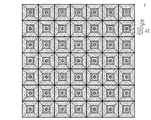
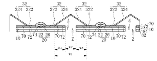
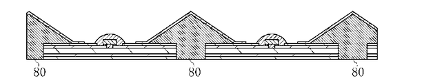
図2Aは実施形態2に係る発光装置の模式的平面図である。図2Bは、図2Aにおいて壁部の先端部にハッチングを施した図である。図2Cは、図2Aにおいて壁部の側面部にハッチングを施した図である。図2Dは、図2Aにおいて壁部の底面部にハッチングを施した図である。図2Eは、基板の貫通孔(第2開口)と光源との位置関係を示す図である。図2Eにおいては、光反射性部材30と接着剤80の図示を省略している。図2Fは図2A中の1F−1F断面を示す図である。図2Fにおいては、発光装置1の上方に配置される部材もあわせて図示している。
[Light emitting device 2 according to the second embodiment]
FIG. 2A is a schematic plan view of the light emitting device according to the second embodiment. FIG. 2B is a view in which the tip end portion of the wall portion is hatched in FIG. 2A. FIG. 2C is a view in which the side surface portion of the wall portion is hatched in FIG. 2A. FIG. 2D is a view in which the bottom surface of the wall portion is hatched in FIG. 2A. FIG. 2E is a diagram showing the positional relationship between the through hole (second opening) of the substrate and the light source. In FIG. 2E, the light reflecting member 30 and the adhesive 80 are not shown. FIG. 2F is a diagram showing a cross section of 1F-1F in FIG. 2A. In FIG. 2F, a member arranged above the light emitting device 1 is also shown.

図2A乃至図2Fに示すように、実施形態2に係る発光装置2は、壁部32の先端部326が、発光装置の上方に配置された部材に接する点で、実施形態1に係る発光装置1と相違する。 As shown in FIGS. 2A to 2F, the light emitting device 2 according to the second embodiment is a light emitting device according to the first embodiment in that the tip portion 326 of the wall portion 32 contacts a member arranged above the light emitting device. Different from 1.

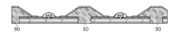
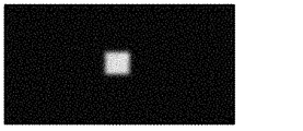
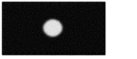
実施形態2に係る発光装置2によれば、実施形態1に係る発光装置1と同様の効果が得られることに加えて、壁部32(発光装置2)と光拡散部材との間の空間を排除することができるため、隣接するセルへの光の漏洩を低減することができる。したがって、当該漏洩によりコントラスト比が低下することを防止することができる。例えば、図5は壁部の先端部が、発光装置の上方に配置される部材に接する場合(実施形態2の場合)において、1つのセルを光源を点灯させながら平面視した場合の一例を示す写真であり、図6は壁部の先端部が、発光装置の上方に配置される部材に接しない場合(比較例の場合)において、1つのセルを光源を点灯させながら平面視した場合の一例を示す写真である。図5、図6において、白く見えるのは光である。図5の光は四角形状であり、図6の光は円形状である。図5、図6に示すように、壁部の先端部326が、発光装置2の上方に配置される部材に接する場合は、接しない場合と比較して、光の形状がセルの平面視形状の相似形になっており、このことは、図5の光の方が図6の光よりも、隣接するセルへの光の漏洩を低減されていることを示す。実施形態2によれば、隣接するセルへの光の漏洩を低減して、コントラスト比の低下が抑制された、見切りのよい発光装置を提供することができる。 According to the light emitting device 2 according to the second embodiment, in addition to obtaining the same effect as the light emitting device 1 according to the first embodiment, the space between the wall portion 32 (light emitting device 2) and the light diffusing member is provided. Since it can be eliminated, it is possible to reduce the leakage of light to the adjacent cell. Therefore, it is possible to prevent the contrast ratio from being lowered due to the leakage. For example, FIG. 5 shows an example in which one cell is viewed in a plan view while the light source is turned on when the tip of the wall portion is in contact with a member arranged above the light emitting device (in the case of the second embodiment). It is a photograph, and FIG. 6 shows an example in which one cell is viewed in a plan view while the light source is turned on when the tip of the wall portion does not contact the member arranged above the light emitting device (in the case of the comparative example). It is a photograph showing. In FIGS. 5 and 6, what appears white is light. The light of FIG. 5 has a quadrangular shape, and the light of FIG. 6 has a circular shape. As shown in FIGS. 5 and 6, when the tip portion 326 of the wall portion is in contact with the member arranged above the light emitting device 2, the shape of the light is the plan view shape of the cell as compared with the case where it is not in contact with the member. This indicates that the light of FIG. 5 has a smaller leakage of light to the adjacent cell than the light of FIG. According to the second embodiment, it is possible to provide a light emitting device having a good visibility by reducing leakage of light to adjacent cells and suppressing a decrease in contrast ratio.

一般に、光反射性部材30の上方に位置する部材を光反射性部材30で支えるという観点からは、光反射性部材30の強度は不十分であるとされる。このため、光反射性部材30の上方に位置する部材は、ピンなどの支持部材を別途設けて、これにより支持するものとされるが、このような支持部材を設けると、光反射性部材30とその上方に位置する部材との間に空間が形成されてしまい、隣接するセルへ光が漏洩する虞がある。しかしながら、実施形態2では、光反射性部材30が有する壁部32の空洞部Y内に樹脂部材80が注入されており、この樹脂部材80が補強材としての役割を果たすことで光反射性部材30の強度を高めることができる。したがって、光反射性部材30の上方に位置する部材を支持するのに十分な強度を光反射性部材30に持たせて、光反射性部材30によりその上方の部材を支持することができる。このため、ピンなどの支持部材を別途設けることを不要にして、光反射性部材30とその上方に位置する部材との間に空間が形成されないようにすることができる。このように、実施形態2によれば、光反射性部材30にその上方の部材が載置されることが可能となるため、見切りが良く、高コントラスト比を実現できる発光装置を提供することができる。 Generally, it is said that the strength of the light-reflecting member 30 is insufficient from the viewpoint of supporting the member located above the light-reflecting member 30 with the light-reflecting member 30. Therefore, the member located above the light-reflecting member 30 is supported by separately providing a support member such as a pin. However, if such a support member is provided, the light-reflecting member 30 is provided. A space is formed between the surface and the member located above the space, and there is a risk that light leaks to the adjacent cell. However, in the second embodiment, the resin member 80 is injected into the cavity Y of the wall portion 32 of the light-reflecting member 30, and the resin member 80 serves as a reinforcing material, so that the light-reflecting member The strength of 30 can be increased. Therefore, the light-reflective member 30 can be provided with sufficient strength to support the member located above the light-reflective member 30, and the member 30 above the light-reflective member 30 can support the member. Therefore, it is not necessary to separately provide a support member such as a pin, and it is possible to prevent a space from being formed between the light-reflecting member 30 and the member located above the light-reflecting member 30. As described above, according to the second embodiment, since the member above the light reflecting member 30 can be mounted on the light reflecting member 30, it is possible to provide a light emitting device capable of achieving a high contrast ratio with good visibility. it can.

壁部32の先端部326は、平面状であることが好ましい。このようにすれば、発光装置の上方に位置する部材を安定的に支持することができる。平面状には平面であるとみなせる場合を含む。なお、壁部32の先端部326は、上記したピンなどの支持部材の形状に形成してもよい。 The tip portion 326 of the wall portion 32 is preferably flat. In this way, the member located above the light emitting device can be stably supported. The plane includes the case where it can be regarded as a plane. The tip portion 326 of the wall portion 32 may be formed in the shape of a support member such as the pin described above.

以上、実施形態2に係る発光装置2について説明したが、その他の構成は実施形態1に係る発光装置1と同じであるので、説明を省略する。 The light emitting device 2 according to the second embodiment has been described above, but since the other configurations are the same as those of the light emitting device 1 according to the first embodiment, the description thereof will be omitted.

[実施形態1に係る発光装置1の製造方法]
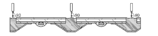
図3A乃至図3Dは、実施形態1に係る発光装置の製造方法を説明する模式的断面図である。以下、図3A乃至図3Dを参照しつつ、実施形態1に係る発光装置1の製造方法を説明する。
[Manufacturing method of light emitting device 1 according to the first embodiment]
3A to 3D are schematic cross-sectional views illustrating a method of manufacturing the light emitting device according to the first embodiment. Hereinafter, the method for manufacturing the light emitting device 1 according to the first embodiment will be described with reference to FIGS. 3A to 3D.

まず、図3Aに示すように、複数の光源20が配置された基板10を準備する。ここで、基板10は、基板10を上下方向に貫通し、第1開口W1の内側に位置する第2開口W2を基板10の上面に有する貫通孔Zを有する。基板10を準備した後に基板10に貫通孔Zを形成してもよいし、あらかじめ貫通孔Zが形成されている基板10を準備してもよい。 First, as shown in FIG. 3A, a substrate 10 on which a plurality of light sources 20 are arranged is prepared. Here, the substrate 10 has a through hole Z that penetrates the substrate 10 in the vertical direction and has a second opening W2 located inside the first opening W1 on the upper surface of the substrate 10. A through hole Z may be formed in the substrate 10 after the substrate 10 is prepared, or a substrate 10 in which the through hole Z is formed in advance may be prepared.

次に、図3Bに示すように、複数の光源20を1つずつまたは2つ以上ずつ囲む壁部32を備えた光反射性部材30を、基板10上に配置する。ここで、壁部32は、例えば、あらかじめ、基板10側に第1開口W1を有する空洞部Yを有する。 Next, as shown in FIG. 3B, a light-reflecting member 30 having a wall portion 32 that surrounds one or two or more of the plurality of light sources 20 is arranged on the substrate 10. Here, the wall portion 32 has, for example, a hollow portion Y having a first opening W1 on the substrate 10 side in advance.

次に、図3Cに示すように、基板10の下面を上側にして、基板10の下面側から貫通孔Zを介して壁部32の空洞部Yに樹脂部材80を注入し、空洞部Yの内壁と、第2開口W2の周縁と第1開口W1の周縁との間に設けられる基板10上面の領域W3と、に樹脂部材80が連続して接するようにする。 Next, as shown in FIG. 3C, the resin member 80 is injected into the hollow portion Y of the wall portion 32 from the lower surface side of the substrate 10 through the through hole Z with the lower surface of the substrate 10 facing upward, and the hollow portion Y is formed. The resin member 80 is in continuous contact with the inner wall and the region W3 on the upper surface of the substrate 10 provided between the peripheral edge of the second opening W2 and the peripheral edge of the first opening W1.

次に、図3Dに示すように、樹脂部材80を硬化(あるいは固化)させる。これにより、空洞部Yの内壁と、第2開口W2の周縁と第1開口W1の周縁との間に設けられる基板10上面の領域W3と、が樹脂部材80により接着され、光反射性部材30が基板10に固定される。 Next, as shown in FIG. 3D, the resin member 80 is cured (or solidified). As a result, the inner wall of the cavity Y and the region W3 on the upper surface of the substrate 10 provided between the peripheral edge of the second opening W2 and the peripheral edge of the first opening W1 are adhered by the resin member 80, and the light reflective member 30 is bonded. Is fixed to the substrate 10.

[実施形態2に係る発光装置2の製造方法]
図4A乃至図4Dは、実施形態2に係る発光装置の製造方法を説明する模式的断面図である。以下、図4A乃至図4Dを参照しつつ、実施形態2に係る発光装置2の製造方法を説明する。
[Manufacturing method of light emitting device 2 according to the second embodiment]
4A to 4D are schematic cross-sectional views illustrating a method of manufacturing the light emitting device according to the second embodiment. Hereinafter, a method for manufacturing the light emitting device 2 according to the second embodiment will be described with reference to FIGS. 4A to 4D.

まず、図4Aに示すように、複数の光源20が配置された基板10を準備する。ここで、基板10は、基板10を上下方向に貫通し、第1開口W1の内側に位置する第2開口W2を基板10の上面に有する貫通孔Zを有する。基板10を準備した後に基板10に貫通孔Zを形成してもよいし、あらかじめ貫通孔Zが形成されている基板10を準備してもよい。 First, as shown in FIG. 4A, a substrate 10 on which a plurality of light sources 20 are arranged is prepared. Here, the substrate 10 has a through hole Z that penetrates the substrate 10 in the vertical direction and has a second opening W2 located inside the first opening W1 on the upper surface of the substrate 10. A through hole Z may be formed in the substrate 10 after the substrate 10 is prepared, or a substrate 10 in which the through hole Z is formed in advance may be prepared.

次に、図4Bに示すように、複数の光源20を1つずつまたは2つ以上ずつ囲む壁部32を備えた光反射性部材30を、基板10上に配置する。ここで、壁部32は、例えば、あらかじめ、基板10側に第1開口W1を有する空洞部Yを有する。 Next, as shown in FIG. 4B, a light-reflecting member 30 having a wall portion 32 that surrounds one or two or more of the plurality of light sources 20 is arranged on the substrate 10. Here, the wall portion 32 has, for example, a hollow portion Y having a first opening W1 on the substrate 10 side in advance.

次に、図4Cに示すように、基板10の下面を上側にして、基板10の下面側から貫通孔Zを介して壁部32の空洞部Yに樹脂部材80を注入し、空洞部Yの内壁と、第2開口W2の周縁と第1開口W1の周縁との間に設けられる基板10上面の領域W3と、に樹脂部材80が連続して接するようにする。 Next, as shown in FIG. 4C, the resin member 80 is injected into the hollow portion Y of the wall portion 32 from the lower surface side of the substrate 10 through the through hole Z with the lower surface of the substrate 10 facing upward, and the hollow portion Y is formed. The resin member 80 is in continuous contact with the inner wall and the region W3 on the upper surface of the substrate 10 provided between the peripheral edge of the second opening W2 and the peripheral edge of the first opening W1.

次に、図4Dに示すように、樹脂部材80を硬化(あるいは固化)させる。これにより、空洞部Yの内壁と、第2開口W2の周縁と第1開口W1の周縁との間に設けられる基板10上面の領域W3と、が樹脂部材80により接着され、光反射性部材30が基板10に固定される。 Next, as shown in FIG. 4D, the resin member 80 is cured (or solidified). As a result, the inner wall of the cavity Y and the region W3 on the upper surface of the substrate 10 provided between the peripheral edge of the second opening W2 and the peripheral edge of the first opening W1 are adhered by the resin member 80, and the light reflective member 30 is bonded. Is fixed to the substrate 10.

本開示に係る発光装置は、直下型バックライト装置として、特に、TVやモニターなどの用途に用いられる直下型バックライト装置として好ましく用いることができる。 The light emitting device according to the present disclosure can be preferably used as a direct type backlight device, particularly as a direct type backlight device used for applications such as TVs and monitors.

1、2 発光装置
10 基板
20 光源
22 発光素子
26 封止部材
28 反射層
30 光反射性部材
32 壁部
322 底面部
324 側面部
326 先端部
40 波長変換部材
52 光拡散部材
54 光学部材
56、58 プリズムシート
60 偏光シート
70、82 反射部材
72、84 導体配線
74 接合部材
80 樹脂部材
X 包囲部
Y 空洞部
Z 貫通孔
W1 第1開口
W2 第2開口
W3 第2開口の周縁と第1開口の周縁との間に設けられる基板上面の領域
1, 2 Light emitting device 10 Substrate 20 Light source 22 Light emitting element 26 Sealing member 28 Reflective layer 30 Light reflective member 32 Wall part 322 Bottom part 324 Side part 326 Tip part 40 Wavelength conversion member 52 Light diffusion member 54 Optical members 56, 58 Prism sheet 60 Polarizing sheet 70, 82 Reflecting member 72, 84 Conductor wiring 74 Joining member 80 Resin member X Surrounding part Y Cavity part Z Through hole W1 First opening W2 Second opening W3 Periphery of second opening and peripheral edge of first opening Area on the upper surface of the substrate provided between

Claims (9)

基板と、
前記基板上に配置される複数の光源と、
前記基板上に配置され、前記複数の光源を1つずつまたは2つ以上ずつ囲む壁部を備えた光反射性部材と、を備えた発光装置であって、
前記壁部は、前記基板側に第1開口を有する空洞部を有し、
前記基板は、前記基板を上下方向に貫通し、前記第1開口の内側に位置する第2開口を前記基板の上面に有する貫通孔を有し、
前記空洞部の内壁と、前記第2開口の周縁と前記第1開口の周縁との間に設けられる前記基板上面の領域と、に樹脂部材が連続して接している発光装置。
With the board
With a plurality of light sources arranged on the substrate,
A light emitting device including a light-reflecting member arranged on the substrate and having a wall portion surrounding the plurality of light sources one by one or two or more.
The wall portion has a hollow portion having a first opening on the substrate side.
The substrate has a through hole that penetrates the substrate in the vertical direction and has a second opening located inside the first opening on the upper surface of the substrate.
A light emitting device in which a resin member is continuously in contact with an inner wall of the cavity and a region on the upper surface of the substrate provided between the peripheral edge of the second opening and the peripheral edge of the first opening.
前記貫通孔それぞれが前記空洞部に繋がる請求項1に記載の発光装置。 The light emitting device according to claim 1, wherein each of the through holes is connected to the cavity. 平面視において、前記樹脂部材は、前記第2開口の周縁から面方向に延びている請求項1または2に記載の発光装置。 The light emitting device according to claim 1 or 2, wherein the resin member extends in the plane direction from the peripheral edge of the second opening in a plan view. 前記光反射性部材は底面部を備え、
前記底面部は前記基板上に配置される請求項1から3のいずれか一項記載の発光装置。
The light-reflecting member has a bottom surface and has a bottom surface.
The light emitting device according to any one of claims 1 to 3, wherein the bottom surface portion is arranged on the substrate.
前記樹脂部材は、前記光源から出射された光を反射する部材である請求項1から4のいずれか一項に記載の発光装置。 The light emitting device according to any one of claims 1 to 4, wherein the resin member is a member that reflects light emitted from the light source. 前記樹脂部材は、前記光源から出射された光を吸収する部材である請求項1から4のいずれか一項に記載の発光装置。 The light emitting device according to any one of claims 1 to 4, wherein the resin member is a member that absorbs light emitted from the light source. 前記壁部の先端部が前記発光装置の上方に配置された部材に接する請求項1から6のいずれか一項に記載の発光装置。 The light emitting device according to any one of claims 1 to 6, wherein the tip end portion of the wall portion is in contact with a member arranged above the light emitting device. 前記複数の光源間の距離は5mm以上25mm以下である請求項1から7のいずれか一項に記載の発光装置。 The light emitting device according to any one of claims 1 to 7, wherein the distance between the plurality of light sources is 5 mm or more and 25 mm or less. 前記壁部の距離は5mm以上25mmである請求項1から8のいずれか一項に記載の発光装置。
The light emitting device according to any one of claims 1 to 8, wherein the distance between the wall portions is 5 mm or more and 25 mm.
JP2019181023A 2019-09-30 2019-09-30 light emitting device Active JP7144682B2 (en)

Priority Applications (3)

Application Number Priority Date Filing Date Title
JP2019181023A JP7144682B2 (en) 2019-09-30 2019-09-30 light emitting device
US17/033,400 US11437429B2 (en) 2019-09-30 2020-09-25 Light emitting device
US17/876,521 US11798977B2 (en) 2019-09-30 2022-07-28 Light emitting device

Applications Claiming Priority (1)

Application Number Priority Date Filing Date Title
JP2019181023A JP7144682B2 (en) 2019-09-30 2019-09-30 light emitting device

Publications (2)

Publication Number Publication Date
JP2021057504A true JP2021057504A (en) 2021-04-08
JP7144682B2 JP7144682B2 (en) 2022-09-30

Family

ID=75272781

Family Applications (1)

Application Number Title Priority Date Filing Date
JP2019181023A Active JP7144682B2 (en) 2019-09-30 2019-09-30 light emitting device

Country Status (1)

Country Link
JP (1) JP7144682B2 (en)

Citations (5)

* Cited by examiner, † Cited by third party
Publication number Priority date Publication date Assignee Title
US4914731A (en) * 1987-08-12 1990-04-03 Chen Shen Yuan Quickly formed light emitting diode display and a method for forming the same
JP2001085748A (en) * 1999-09-14 2001-03-30 Matsushita Electric Works Ltd Light-emitting device
JP2013015768A (en) * 2011-07-06 2013-01-24 Sharp Corp Reflection member, light-emitting device and display
JP2017034119A (en) * 2015-08-03 2017-02-09 シチズン電子株式会社 Led light-emitting element
JP2017157278A (en) * 2016-02-29 2017-09-07 日亜化学工業株式会社 Light emitting device and surface light emitting device using light emitting device

Patent Citations (5)

* Cited by examiner, † Cited by third party
Publication number Priority date Publication date Assignee Title
US4914731A (en) * 1987-08-12 1990-04-03 Chen Shen Yuan Quickly formed light emitting diode display and a method for forming the same
JP2001085748A (en) * 1999-09-14 2001-03-30 Matsushita Electric Works Ltd Light-emitting device
JP2013015768A (en) * 2011-07-06 2013-01-24 Sharp Corp Reflection member, light-emitting device and display
JP2017034119A (en) * 2015-08-03 2017-02-09 シチズン電子株式会社 Led light-emitting element
JP2017157278A (en) * 2016-02-29 2017-09-07 日亜化学工業株式会社 Light emitting device and surface light emitting device using light emitting device

Also Published As

Publication number Publication date
JP7144682B2 (en) 2022-09-30

Similar Documents

Publication Publication Date Title
JP7177331B2 (en) light emitting device
CN109427758B (en) Light emitting device
JP7252483B2 (en) Light-emitting device, integrated light-emitting device and light-emitting module
JP6868388B2 (en) Light emitting device and integrated light emitting device
JP5482378B2 (en) Light emitting device
TW201830101A (en) Light emitting device
TWI817708B (en) Light source
US9728685B2 (en) Light emitting device and lighting device including same
EP3154096A1 (en) Light-emitting device, integrated light-emitting device having the same, and light-emitting module incorporating the same
JP7174216B2 (en) Light-emitting modules and integrated light-emitting modules
JP2010272847A5 (en)
JP5962285B2 (en) Light emitting device and manufacturing method thereof
JP2014093311A (en) Light-emitting device and manufacturing method thereof
JP2019046789A (en) Light-emitting device
JP4938255B2 (en) Light emitting element storage package, light source, and light emitting device
JP2022012079A (en) Light-emitting module, and liquid crystal display device
JP2017118081A (en) Light-emitting device
JP2010225754A (en) Semiconductor light emitting device
JP2009206228A (en) Side emission type light emitting device and manufacturing method thereof, and lighting device
US11798977B2 (en) Light emitting device
JP2009224376A (en) Side surface type light emitting device and method of manufacturing the same
JP7144682B2 (en) light emitting device
JP7014966B2 (en) Luminescent device
JP7144683B2 (en) light emitting device
JP2017117831A (en) Light-emitting device and power feeding connector for the same

Legal Events

Date Code Title Description
A621 Written request for application examination

Free format text: JAPANESE INTERMEDIATE CODE: A621

Effective date: 20210803

A977 Report on retrieval

Free format text: JAPANESE INTERMEDIATE CODE: A971007

Effective date: 20220427

A131 Notification of reasons for refusal

Free format text: JAPANESE INTERMEDIATE CODE: A131

Effective date: 20220510

A521 Request for written amendment filed

Free format text: JAPANESE INTERMEDIATE CODE: A523

Effective date: 20220629

TRDD Decision of grant or rejection written
A01 Written decision to grant a patent or to grant a registration (utility model)

Free format text: JAPANESE INTERMEDIATE CODE: A01

Effective date: 20220816

A61 First payment of annual fees (during grant procedure)

Free format text: JAPANESE INTERMEDIATE CODE: A61

Effective date: 20220829

R151 Written notification of patent or utility model registration

Ref document number: 7144682

Country of ref document: JP

Free format text: JAPANESE INTERMEDIATE CODE: R151