JP2021052182A - Semiconductor processing device - Google Patents
Semiconductor processing device Download PDFInfo
- Publication number
- JP2021052182A JP2021052182A JP2020155939A JP2020155939A JP2021052182A JP 2021052182 A JP2021052182 A JP 2021052182A JP 2020155939 A JP2020155939 A JP 2020155939A JP 2020155939 A JP2020155939 A JP 2020155939A JP 2021052182 A JP2021052182 A JP 2021052182A
- Authority
- JP
- Japan
- Prior art keywords
- process control
- control chamber
- reactor
- valve
- raw material
- Prior art date
- Legal status (The legal status is an assumption and is not a legal conclusion. Google has not performed a legal analysis and makes no representation as to the accuracy of the status listed.)
- Granted
Links
Images
Classifications
-
- C—CHEMISTRY; METALLURGY
- C23—COATING METALLIC MATERIAL; COATING MATERIAL WITH METALLIC MATERIAL; CHEMICAL SURFACE TREATMENT; DIFFUSION TREATMENT OF METALLIC MATERIAL; COATING BY VACUUM EVAPORATION, BY SPUTTERING, BY ION IMPLANTATION OR BY CHEMICAL VAPOUR DEPOSITION, IN GENERAL; INHIBITING CORROSION OF METALLIC MATERIAL OR INCRUSTATION IN GENERAL
- C23C—COATING METALLIC MATERIAL; COATING MATERIAL WITH METALLIC MATERIAL; SURFACE TREATMENT OF METALLIC MATERIAL BY DIFFUSION INTO THE SURFACE, BY CHEMICAL CONVERSION OR SUBSTITUTION; COATING BY VACUUM EVAPORATION, BY SPUTTERING, BY ION IMPLANTATION OR BY CHEMICAL VAPOUR DEPOSITION, IN GENERAL
- C23C16/00—Chemical coating by decomposition of gaseous compounds, without leaving reaction products of surface material in the coating, i.e. chemical vapour deposition [CVD] processes
- C23C16/44—Chemical coating by decomposition of gaseous compounds, without leaving reaction products of surface material in the coating, i.e. chemical vapour deposition [CVD] processes characterised by the method of coating
- C23C16/448—Chemical coating by decomposition of gaseous compounds, without leaving reaction products of surface material in the coating, i.e. chemical vapour deposition [CVD] processes characterised by the method of coating characterised by the method used for generating reactive gas streams, e.g. by evaporation or sublimation of precursor materials
-
- C—CHEMISTRY; METALLURGY
- C23—COATING METALLIC MATERIAL; COATING MATERIAL WITH METALLIC MATERIAL; CHEMICAL SURFACE TREATMENT; DIFFUSION TREATMENT OF METALLIC MATERIAL; COATING BY VACUUM EVAPORATION, BY SPUTTERING, BY ION IMPLANTATION OR BY CHEMICAL VAPOUR DEPOSITION, IN GENERAL; INHIBITING CORROSION OF METALLIC MATERIAL OR INCRUSTATION IN GENERAL
- C23C—COATING METALLIC MATERIAL; COATING MATERIAL WITH METALLIC MATERIAL; SURFACE TREATMENT OF METALLIC MATERIAL BY DIFFUSION INTO THE SURFACE, BY CHEMICAL CONVERSION OR SUBSTITUTION; COATING BY VACUUM EVAPORATION, BY SPUTTERING, BY ION IMPLANTATION OR BY CHEMICAL VAPOUR DEPOSITION, IN GENERAL
- C23C16/00—Chemical coating by decomposition of gaseous compounds, without leaving reaction products of surface material in the coating, i.e. chemical vapour deposition [CVD] processes
- C23C16/44—Chemical coating by decomposition of gaseous compounds, without leaving reaction products of surface material in the coating, i.e. chemical vapour deposition [CVD] processes characterised by the method of coating
- C23C16/455—Chemical coating by decomposition of gaseous compounds, without leaving reaction products of surface material in the coating, i.e. chemical vapour deposition [CVD] processes characterised by the method of coating characterised by the method used for introducing gases into reaction chamber or for modifying gas flows in reaction chamber
- C23C16/45561—Gas plumbing upstream of the reaction chamber
-
- C—CHEMISTRY; METALLURGY
- C23—COATING METALLIC MATERIAL; COATING MATERIAL WITH METALLIC MATERIAL; CHEMICAL SURFACE TREATMENT; DIFFUSION TREATMENT OF METALLIC MATERIAL; COATING BY VACUUM EVAPORATION, BY SPUTTERING, BY ION IMPLANTATION OR BY CHEMICAL VAPOUR DEPOSITION, IN GENERAL; INHIBITING CORROSION OF METALLIC MATERIAL OR INCRUSTATION IN GENERAL
- C23C—COATING METALLIC MATERIAL; COATING MATERIAL WITH METALLIC MATERIAL; SURFACE TREATMENT OF METALLIC MATERIAL BY DIFFUSION INTO THE SURFACE, BY CHEMICAL CONVERSION OR SUBSTITUTION; COATING BY VACUUM EVAPORATION, BY SPUTTERING, BY ION IMPLANTATION OR BY CHEMICAL VAPOUR DEPOSITION, IN GENERAL
- C23C14/00—Coating by vacuum evaporation, by sputtering or by ion implantation of the coating forming material
- C23C14/22—Coating by vacuum evaporation, by sputtering or by ion implantation of the coating forming material characterised by the process of coating
- C23C14/54—Controlling or regulating the coating process
-
- C—CHEMISTRY; METALLURGY
- C23—COATING METALLIC MATERIAL; COATING MATERIAL WITH METALLIC MATERIAL; CHEMICAL SURFACE TREATMENT; DIFFUSION TREATMENT OF METALLIC MATERIAL; COATING BY VACUUM EVAPORATION, BY SPUTTERING, BY ION IMPLANTATION OR BY CHEMICAL VAPOUR DEPOSITION, IN GENERAL; INHIBITING CORROSION OF METALLIC MATERIAL OR INCRUSTATION IN GENERAL
- C23C—COATING METALLIC MATERIAL; COATING MATERIAL WITH METALLIC MATERIAL; SURFACE TREATMENT OF METALLIC MATERIAL BY DIFFUSION INTO THE SURFACE, BY CHEMICAL CONVERSION OR SUBSTITUTION; COATING BY VACUUM EVAPORATION, BY SPUTTERING, BY ION IMPLANTATION OR BY CHEMICAL VAPOUR DEPOSITION, IN GENERAL
- C23C16/00—Chemical coating by decomposition of gaseous compounds, without leaving reaction products of surface material in the coating, i.e. chemical vapour deposition [CVD] processes
- C23C16/44—Chemical coating by decomposition of gaseous compounds, without leaving reaction products of surface material in the coating, i.e. chemical vapour deposition [CVD] processes characterised by the method of coating
- C23C16/448—Chemical coating by decomposition of gaseous compounds, without leaving reaction products of surface material in the coating, i.e. chemical vapour deposition [CVD] processes characterised by the method of coating characterised by the method used for generating reactive gas streams, e.g. by evaporation or sublimation of precursor materials
- C23C16/4481—Chemical coating by decomposition of gaseous compounds, without leaving reaction products of surface material in the coating, i.e. chemical vapour deposition [CVD] processes characterised by the method of coating characterised by the method used for generating reactive gas streams, e.g. by evaporation or sublimation of precursor materials by evaporation using carrier gas in contact with the source material
-
- C—CHEMISTRY; METALLURGY
- C23—COATING METALLIC MATERIAL; COATING MATERIAL WITH METALLIC MATERIAL; CHEMICAL SURFACE TREATMENT; DIFFUSION TREATMENT OF METALLIC MATERIAL; COATING BY VACUUM EVAPORATION, BY SPUTTERING, BY ION IMPLANTATION OR BY CHEMICAL VAPOUR DEPOSITION, IN GENERAL; INHIBITING CORROSION OF METALLIC MATERIAL OR INCRUSTATION IN GENERAL
- C23C—COATING METALLIC MATERIAL; COATING MATERIAL WITH METALLIC MATERIAL; SURFACE TREATMENT OF METALLIC MATERIAL BY DIFFUSION INTO THE SURFACE, BY CHEMICAL CONVERSION OR SUBSTITUTION; COATING BY VACUUM EVAPORATION, BY SPUTTERING, BY ION IMPLANTATION OR BY CHEMICAL VAPOUR DEPOSITION, IN GENERAL
- C23C16/00—Chemical coating by decomposition of gaseous compounds, without leaving reaction products of surface material in the coating, i.e. chemical vapour deposition [CVD] processes
- C23C16/44—Chemical coating by decomposition of gaseous compounds, without leaving reaction products of surface material in the coating, i.e. chemical vapour deposition [CVD] processes characterised by the method of coating
- C23C16/455—Chemical coating by decomposition of gaseous compounds, without leaving reaction products of surface material in the coating, i.e. chemical vapour deposition [CVD] processes characterised by the method of coating characterised by the method used for introducing gases into reaction chamber or for modifying gas flows in reaction chamber
- C23C16/45523—Pulsed gas flow or change of composition over time
- C23C16/45525—Atomic layer deposition [ALD]
- C23C16/45544—Atomic layer deposition [ALD] characterized by the apparatus
-
- C—CHEMISTRY; METALLURGY
- C23—COATING METALLIC MATERIAL; COATING MATERIAL WITH METALLIC MATERIAL; CHEMICAL SURFACE TREATMENT; DIFFUSION TREATMENT OF METALLIC MATERIAL; COATING BY VACUUM EVAPORATION, BY SPUTTERING, BY ION IMPLANTATION OR BY CHEMICAL VAPOUR DEPOSITION, IN GENERAL; INHIBITING CORROSION OF METALLIC MATERIAL OR INCRUSTATION IN GENERAL
- C23C—COATING METALLIC MATERIAL; COATING MATERIAL WITH METALLIC MATERIAL; SURFACE TREATMENT OF METALLIC MATERIAL BY DIFFUSION INTO THE SURFACE, BY CHEMICAL CONVERSION OR SUBSTITUTION; COATING BY VACUUM EVAPORATION, BY SPUTTERING, BY ION IMPLANTATION OR BY CHEMICAL VAPOUR DEPOSITION, IN GENERAL
- C23C16/00—Chemical coating by decomposition of gaseous compounds, without leaving reaction products of surface material in the coating, i.e. chemical vapour deposition [CVD] processes
- C23C16/44—Chemical coating by decomposition of gaseous compounds, without leaving reaction products of surface material in the coating, i.e. chemical vapour deposition [CVD] processes characterised by the method of coating
- C23C16/455—Chemical coating by decomposition of gaseous compounds, without leaving reaction products of surface material in the coating, i.e. chemical vapour deposition [CVD] processes characterised by the method of coating characterised by the method used for introducing gases into reaction chamber or for modifying gas flows in reaction chamber
- C23C16/45557—Pulsed pressure or control pressure
-
- C—CHEMISTRY; METALLURGY
- C23—COATING METALLIC MATERIAL; COATING MATERIAL WITH METALLIC MATERIAL; CHEMICAL SURFACE TREATMENT; DIFFUSION TREATMENT OF METALLIC MATERIAL; COATING BY VACUUM EVAPORATION, BY SPUTTERING, BY ION IMPLANTATION OR BY CHEMICAL VAPOUR DEPOSITION, IN GENERAL; INHIBITING CORROSION OF METALLIC MATERIAL OR INCRUSTATION IN GENERAL
- C23C—COATING METALLIC MATERIAL; COATING MATERIAL WITH METALLIC MATERIAL; SURFACE TREATMENT OF METALLIC MATERIAL BY DIFFUSION INTO THE SURFACE, BY CHEMICAL CONVERSION OR SUBSTITUTION; COATING BY VACUUM EVAPORATION, BY SPUTTERING, BY ION IMPLANTATION OR BY CHEMICAL VAPOUR DEPOSITION, IN GENERAL
- C23C16/00—Chemical coating by decomposition of gaseous compounds, without leaving reaction products of surface material in the coating, i.e. chemical vapour deposition [CVD] processes
- C23C16/44—Chemical coating by decomposition of gaseous compounds, without leaving reaction products of surface material in the coating, i.e. chemical vapour deposition [CVD] processes characterised by the method of coating
- C23C16/52—Controlling or regulating the coating process
-
- G—PHYSICS
- G05—CONTROLLING; REGULATING
- G05B—CONTROL OR REGULATING SYSTEMS IN GENERAL; FUNCTIONAL ELEMENTS OF SUCH SYSTEMS; MONITORING OR TESTING ARRANGEMENTS FOR SUCH SYSTEMS OR ELEMENTS
- G05B11/00—Automatic controllers
- G05B11/01—Automatic controllers electric
- G05B11/36—Automatic controllers electric with provision for obtaining particular characteristics, e.g. proportional, integral, differential
- G05B11/42—Automatic controllers electric with provision for obtaining particular characteristics, e.g. proportional, integral, differential for obtaining a characteristic which is both proportional and time-dependent, e.g. P. I., P. I. D.
-
- H10P14/24—
-
- H10P14/6334—
Landscapes
- Chemical & Material Sciences (AREA)
- Engineering & Computer Science (AREA)
- Chemical Kinetics & Catalysis (AREA)
- Mechanical Engineering (AREA)
- Organic Chemistry (AREA)
- Metallurgy (AREA)
- Materials Engineering (AREA)
- General Chemical & Material Sciences (AREA)
- General Physics & Mathematics (AREA)
- Physics & Mathematics (AREA)
- Automation & Control Theory (AREA)
- Chemical Vapour Deposition (AREA)
- Condensed Matter Physics & Semiconductors (AREA)
- Manufacturing & Machinery (AREA)
- Computer Hardware Design (AREA)
- Microelectronics & Electronic Packaging (AREA)
- Power Engineering (AREA)
Abstract
【課題】反応チャンバーの上流のプロセス制御チャンバを含む半導体加工装置を提供する。
【解決手段】半導体加工装置1は、反応器21と、気化された固体反応物質を反応器に供給するように構成された固体原料容器2とを含む。プロセス制御チャンバー10は、固体原料容器と反応器との間に配置される。該装置は、プロセス制御チャンバーの上流に反応物質ガスバルブ7を含む。制御システム34は、プロセス制御チャンバー内の測定された圧力のフィードバックに少なくとも部分的に基づいて、該バルブの動作を制御する。
【選択図】図1PROBLEM TO BE SOLVED: To provide a semiconductor processing apparatus including a process control chamber upstream of a reaction chamber.
A semiconductor processing apparatus 1 includes a reactor 21 and a solid raw material container 2 configured to supply a vaporized solid reactant to the reactor. The process control chamber 10 is arranged between the solid raw material container and the reactor. The device includes a reactant gas valve 7 upstream of the process control chamber. The control system 34 controls the operation of the valve based at least in part on the feedback of the measured pressure in the process control chamber.
[Selection diagram] Fig. 1
Description
関連出願の相互参照
本出願は、2019年9月20日に出願された米国仮特許出願第62/903,566号の優先権を主張するものであり、その内容全体は参照により、かつすべての目的のためにその全体が本明細書に組み込まれる。
Cross-reference to related applications This application claims the priority of US Provisional Patent Application No. 62 / 903,566 filed on September 20, 2019, the entire contents of which are by reference and in full. The whole is incorporated herein by purpose.
本技術分野は、半導体加工装置に関連し、特に、反応チャンバーの上流のプロセス制御チャンバーを含む半導体加工装置に関する。 The present technical field relates to semiconductor processing equipment, and particularly to semiconductor processing equipment including a process control chamber upstream of a reaction chamber.
半導体加工中、様々な反応物質蒸気が反応チャンバーに供給される。一部の用途において、周囲圧力および温度で固相の原料化学物質の反応物質蒸気が使用される。これらの固体原料物質を熱して昇華させて、蒸着などの反応プロセスのために気化された反応物質を生成することができる。化学蒸着(CVD)は、反応チャンバーへの反応物質蒸気の連続的な流れの供給を必要とする場合があり、一方で原子層堆積(ALD)、パルスCVD、およびそれらの混成物は、所望の構成に応じて、時間分割および空間分割されたパルス化されるプロセスを含み、反応チャンバーへの連続的な流れまたはパルス供給を必要とする場合がある。このような固体物質からの気相反応物質はまた、半導体産業の他のタイプの化学反応(例えば、エッチング、ドーピングなど)、および他の様々な産業の他のタイプの化学反応に有用でありうる。しかしながら、蒸発温度および分解温度の間の小さなプロセスウィンドウ、低い蒸気圧、ならびにかかる固体反応物質のための均一なドース量の必要性に部分的に起因して、固体反応物質源からの気相送達に対する制御の改善が未だに継続的に要求される。 During semiconductor processing, various reactant vapors are supplied to the reaction chamber. In some applications, reactant vapors of solid phase raw material chemicals at ambient pressure and temperature are used. These solid raw materials can be heated and sublimated to produce vaporized reactants for reaction processes such as vapor deposition. Chemical vapor deposition (CVD) may require the supply of a continuous stream of reactant vapors to the reaction chamber, while atomic layer deposition (ALD), pulse CVD, and mixtures thereof are desired. Depending on the configuration, it may include time-divided and spatially-divided pulsed processes, requiring continuous flow or pulse delivery to the reaction chamber. Gas phase reactants from such solid materials may also be useful for other types of chemical reactions in the semiconductor industry (eg, etching, doping, etc.), and for other types of chemical reactions in various other industries. .. However, due in part to the small process window between the evaporation and decomposition temperatures, the low vapor pressure, and the need for a uniform dose amount for such solid reactants, vapor phase delivery from solid reactant sources. There is still a continuous need for improved control over.
一実施形態では、半導体加工装置が開示される。半導体加工装置は、反応器と、気化された反応物質を反応器に供給するように構成された固体原料容器とを含む。半導体加工装置は、固体原料容器と反応器との間に、固体原料容器と反応器とに流体連通するプロセス制御チャンバーを含みうる。プロセス制御バルブは、固体原料容器とプロセス制御チャンバーとの間でプロセス制御チャンバーの上流に配置することができる。半導体加工装置は、プロセス制御チャンバー内の測定された圧力のフィードバックに少なくとも部分的に基づいて、プロセス制御バルブの動作を制御するように構成された制御システムを含みうる。 In one embodiment, a semiconductor processing apparatus is disclosed. The semiconductor processing apparatus includes a reactor and a solid raw material container configured to supply the vaporized reactants to the reactor. The semiconductor processing apparatus may include a process control chamber for fluid communication between the solid raw material container and the reactor between the solid raw material container and the reactor. The process control valve can be located upstream of the process control chamber between the solid raw material container and the process control chamber. The semiconductor processing equipment may include a control system configured to control the operation of the process control valve, at least in part, based on the feedback of the measured pressure in the process control chamber.
別の実施形態では、気化された反応物質を形成するための装置が開示される。装置は、第一の温度で第一の熱ゾーン内に配置された固体原料容器を含むことができる。装置は、固体原料容器の下流に固体原料容器と流体連通してプロセス制御チャンバーを含むことができる。プロセス制御チャンバーは、第一の温度よりも高い第二の温度で第二の熱ゾーン内に配置され、かつ気化された反応物質を、プロセス制御チャンバーの下流の反応器に移送するように構成されうる。装置は、プロセス制御チャンバーの上流で、かつ固体原料容器とプロセス制御チャンバーとの間の第二の熱ゾーン内に配置されたプロセス制御バルブを含みうる。制御システムは、プロセス制御チャンバー内の測定された圧力のフィードバックに少なくとも部分的に基づいて、プロセス制御バルブの動作を制御するように構成されうる。 In another embodiment, an apparatus for forming a vaporized reactant is disclosed. The device can include a solid raw material container located in a first thermal zone at a first temperature. The device can include a process control chamber in fluid communication with the solid raw material container downstream of the solid raw material container. The process control chamber is located in the second thermal zone at a second temperature higher than the first temperature and is configured to transfer vaporized reactants to the reactor downstream of the process control chamber. sell. The apparatus may include a process control valve located upstream of the process control chamber and in a second thermal zone between the solid raw material container and the process control chamber. The control system may be configured to control the operation of the process control valve based at least in part on the feedback of the measured pressure in the process control chamber.
別の実施形態では、気化された反応物質を形成する方法が開示される。方法は、固体反応物質を気化して反応物質蒸気を形成することを含みうる。方法は、反応物質蒸気をプロセス制御チャンバーに移送することを含みうる。方法は、プロセス制御チャンバー内の測定された圧力のフィードバックに少なくとも部分的に基づいて、プロセス制御チャンバーの上流のプロセス制御バルブの動作を制御することを含みうる。方法は、反応物質蒸気をプロセス制御チャンバーから反応チャンバーに移送することを含みうる。 In another embodiment, a method of forming a vaporized reactant is disclosed. The method may include vaporizing the solid reactant to form a reactant vapor. The method may include transferring the reactant vapor to a process control chamber. The method may include controlling the operation of the process control valve upstream of the process control chamber, at least in part, based on the feedback of the measured pressure in the process control chamber. The method may include transferring the reactant vapor from the process control chamber to the reaction chamber.
ここで、本発明のこれらおよびその他の特徴、態様、および利点を、本発明を限定するのではなく例示することを意図する、幾つかの実施形態の図面を参照して記述する。 Here, these and other features, aspects, and advantages of the invention are described with reference to the drawings of some embodiments intended to illustrate, but not limit, the invention.
本明細書に開示される実施形態は、堆積前駆体などの固体反応物質の気相送達の制御を改善する半導体加工装置に関する。本明細書に開示される実施形態は、原子層堆積(ALD)装置、化学蒸着(CVD)装置、このようなパルス化されるプロセスの変形のために構成された装置、有機金属CVD(MOCVD)装置、物理蒸着装置(PVD)などを含む、任意の好適なタイプの半導体加工装置と併せて使用することができる。 The embodiments disclosed herein relate to semiconductor processing equipment that improves control of gas phase delivery of solid reactants such as sedimentary precursors. The embodiments disclosed herein include atomic layer deposition (ALD) equipment, chemical vapor deposition (CVD) equipment, equipment configured for the transformation of such pulsed processes, metalorganic metal deposition (MOCVD). It can be used in conjunction with any suitable type of semiconductor processing equipment, including equipment, physical vapor deposition equipment (PVD), and the like.
例えば、ALDは、基材上に非常に均一な薄膜を成長させるための方法である。時間分割ALD反応器では、基材は不純物のない反応空間内に置かれ、少なくとも二つの異なる反応物質(前駆体、または他の反応物質蒸気)が気相で交互にかつ反復的に反応空間内に注入される。反応物質蒸気はしたがって、一つ以上の反応物質および一つ以上の溶媒を含む、蒸気を含むことができる。膜の成長が、基材の表面上で発生する交互の表面反応に基づいて、原子または分子の固体層を形成するのは、反応物質と基材の温度とが、交互に注入された気相反応物質の分子が、基材上でのみその表面層と反応するように選択されるからである。反応物質は、各注入サイクル中に表面が飽和に近づくのに十分なほど高いドーズ量で注入される。したがって、プロセスは、出発物質の濃度に依存せず、理論上は自己調節的であり、それによって、極めて高い膜均一性および単一の原子または分子層の厚さ精度を達成することが可能である。同様の結果が空間分割ALD反応器で得られ、基材は異なる反応物質に交互に曝露されるゾーンに移動される。反応物質は、成長する膜(前駆体)に寄与すること、および/またはリガンドを酸化して、還元して、もしくは前駆体の吸着種から除去して、後続の反応物質の反応もしくは吸着を促進するなどの他の機能を果たすことができる。ALD方法は、元素薄膜および化合物薄膜の両方の成長に使用することができる。ALDは、サイクルで繰り返される代替の二つ以上の反応物質を含むことができ、異なるサイクルは、異なる数の反応物質を有することができる。真のALD反応は、サイクルごとに単層よりも少なく生成する傾向がある。ALD原理の実際の用途は、真の飽和制限および単層制限(true saturation and monolayer limitations)からの実世界の逸脱を有する傾向があり、また混成または変形プロセスは、ALDの共形性および制御の利点の一部またはすべてを達成しながら、より高い堆積率を得ることができる。 For example, ALD is a method for growing a very uniform thin film on a substrate. In a time-divided ALD reactor, the substrate is placed in an impurity-free reaction space, with at least two different reactants (precursor, or other reactant vapor) alternating and iteratively in the gas phase. Is injected into. Reactant vapors can therefore include vapors, including one or more reactants and one or more solvents. It is the gas phase in which the reactants and the temperature of the substrate are alternately injected that the growth of the membrane forms a solid layer of atoms or molecules based on the alternating surface reactions that occur on the surface of the substrate. This is because the molecules of the reactants are selected to react with their surface layer only on the substrate. The reactants are injected during each injection cycle with a dose high enough to bring the surface close to saturation. Therefore, the process is independent of the concentration of starting material and is theoretically self-regulating, which makes it possible to achieve extremely high membrane uniformity and thickness accuracy of a single atom or molecular layer. is there. Similar results are obtained with a spatially divided ALD reactor, where the substrate is moved to zones that are alternately exposed to different reactants. The reactants contribute to the growing membrane (precursor) and / or oxidize and reduce the ligand or remove it from the adsorbed species of the precursor to promote the reaction or adsorption of subsequent reactants. Can perform other functions such as The ALD method can be used for the growth of both elemental and compound thin films. The ALD can include two or more alternative reactants that are repeated in the cycle, and different cycles can have different numbers of reactants. True ALD reactions tend to produce less than a single layer per cycle. Practical applications of the ALD principle tend to have real-world deviations from true saturation limits and monolayer limits, and hybrid or deformation processes of ALD symmetry and control. Higher deposition rates can be obtained while achieving some or all of the benefits.
本明細書で説明するように、固体反応物質源(または反応物質溶媒混合物)を加熱容器内で昇華させて、反応器または反応チャンバーに送達される反応物質蒸気を形成することができる。しかしながら、固体反応物質材料の昇華は、低速プロセス、例えば、液体反応物質蒸発システムよりも桁違いに低速、とすることができる。さらに、固体反応物質材料の昇華速度は、原料容器形状、固体前駆体粒子の表面積、不規則形状の固体反応物質粒子、および半導体加工システムのその他の構成要素に応じて変化しうる。例えば、一部の事例では、固体反応物質粒子の表面積は、固体粒子凝集体に応じて動作中に変化することがある。昇華速度は動作中に経時的に変化することがあり、反応チャンバーへの気化された反応物質の供給もまた、一貫性がなく、可変であってもよい。 As described herein, a solid reactant source (or reactant solvent mixture) can be sublimated in a heating vessel to form reactant vapors delivered to the reactor or reaction chamber. However, the sublimation of solid reactant materials can be slower processes, eg, orders of magnitude slower than liquid reactant evaporation systems. In addition, the sublimation rate of the solid reactant material can vary depending on the shape of the raw material container, the surface area of the solid precursor particles, the irregularly shaped solid reactant particles, and other components of the semiconductor processing system. For example, in some cases, the surface area of solid reactant particles may change during operation depending on the solid particle aggregates. The sublimation rate may change over time during operation, and the supply of vaporized reactants to the reaction chamber may also be inconsistent and variable.
一部の半導体加工装置では、固体原料反応物質ドーズ量は、固体原料容器内の蒸気圧、固体原料容器を通る流量、およびパルス時間を制御することによって制御されうる。例えば、マスターフローコントローラ(MFC)または圧力コントローラなどの制御装置を、固体原料容器の上流に提供することができる。制御装置は、制御装置が高温環境と適合しないため、固体反応物質源を昇華させるために使用される熱源から離れていてもよい。上述のように、昇華速度が変化する場合、パルス当たりで送達される反応物質の量は変化してもよく、このことはウエハ収率を減少させ、コストを増加させうる。したがって、反応器への気化された固体反応物質の供給の改善が、未だ継続的に必要とされている。 In some semiconductor processing equipment, the dose amount of solid raw material reactants can be controlled by controlling the vapor pressure in the solid raw material container, the flow rate through the solid raw material container, and the pulse time. For example, a control device such as a master flow controller (MFC) or a pressure controller can be provided upstream of the solid raw material container. The controller may be remote from the heat source used to sublimate the solid reactant source as the controller is incompatible with the high temperature environment. As mentioned above, if the sublimation rate changes, the amount of reactants delivered per pulse may vary, which can reduce wafer yields and increase costs. Therefore, there is still a continuous need to improve the supply of vaporized solid reactants to the reactor.
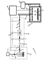
図1は、様々な実施形態による半導体加工装置1の概略的なシステム図である。装置1は、気化された固体反応物質を反応器21に供給するように構成された固体原料容器2を備えることができる。固体原料容器2は、固体反応物質源粒子の気化された反応物質への昇華を引き起こすヒーターを含むことができる。本明細書で開示されている装置1で使用されうる固体原料容器の例は、米国特許第7,122,085号および第8,137,462号、ならびに米国特許出願公開第2018/0094350号(それぞれの内容全体は参照により、かつすべての目的のためにその全体が本明細書に組み込まれる)に示され、記載される固体原料容器を含む、任意の適切なタイプの固体原料容器とすることができる。 FIG. 1 is a schematic system diagram of the semiconductor processing apparatus 1 according to various embodiments. The apparatus 1 can include a solid raw material container 2 configured to supply the vaporized solid reactant to the reactor 21. The solid feedstock container 2 can include a heater that causes the solid reactant source particles to sublimate into vaporized reactants. Examples of solid raw material containers that can be used in apparatus 1 disclosed herein are US Pat. Nos. 7,122,085 and 8,137,462, and US Patent Application Publication No. 2018/0094350 ( The entire contents of each shall be any suitable type of solid raw material container, including the solid raw material containers shown and described herein by reference and in their entirety for all purposes. Can be done.
不活性ガス源3は、不活性キャリアガスを不活性ガスライン4に沿って、固体原料容器2に供給できる。様々な実施形態では、ガスマスフローコントローラ(MFC)は、不活性ガスライン4に沿ったガスの供給を計量できる。不活性ガスバルブ6は、不活性ガスライン4に沿って設けられ、不活性ガスの固体原料容器2への流れを調整しうる。不活性ガスバルブ6は、いくつかの実施形態では、複数の流れコンダクタンス設定を有する調節可能なバルブを備えることができる。他の実施形態では、不活性ガスバルブ6は、バルブ6が不活性ガスライン4に沿った不活性ガスの流れを許可または遮断する、バイナリー開閉バルブを含むことができる。図1の実施形態では、不活性ガスは、反応物質蒸気を反応器21に供給する、および運ぶのを支援することができる。
The
固体原料容器2の圧力および温度は、固体反応物質粒子が反応物質蒸気へと昇華されるように制御されうる。図示した実施形態では、不活性ガス源3からの不活性キャリアガスは、反応物質蒸気を反応器21に運ぶまたは推進する役割を果たすことができる。他の実施形態では、反応物質蒸気は、加熱された反応物質および/または蒸気を吸い込む下流真空源の蒸気圧に基づいて、別個の不活性キャリアガス供給を使用せずに、供給ライン5に沿って供給されうる。別個の不活性ガス源を省略して、反応物質蒸気を供給ライン5を通して運ぶことで、装置1に関連する費用および複雑さを有益に低減することができる。反応物質蒸気を、反応物質蒸気供給ライン5に沿ってフィルター8に供給することができる。反応物質ガスバルブ7は、固体原料容器2からフィルター8への反応物質蒸気の供給を計量するために提供されうる。反応物質ガスバルブ7は、調節可能なバルブまたはバイナリー開閉バルブなどの任意の適切なタイプのバルブを備えることができる。図示した実施形態では、例えば、反応物質ガスバルブ7は、例えば、バイナリー開閉バルブのような、容器隔離バルブを備えることができる。フィルター8は、不完全な昇華に起因して存在する液体小滴または固体微粒子を捕捉および気化するように構成されうる。
The pressure and temperature of the solid feedstock container 2 can be controlled so that the solid reactant particles are sublimated into the reactant vapor. In the illustrated embodiment, the Inactive Carrier Gas from the
プロセス制御チャンバー10は、固体原料容器2と反応器21との間に配置されうる。プロセス制御チャンバー10は、反応物質供給ライン5に沿って反応器21に供給される、反応物質蒸気の量を計量または制御することができる。プロセス制御チャンバー10は、反応物質が反応器21に送達される前に蒸気形態で収集される中間ボリュームとして機能することができる。プロセス制御チャンバー10を使用して反応器21への反応物質蒸気の供給を制御することは、反応器21に対する反応物質蒸気ドース量のより正確な制御を有益に可能にすることができる。
The
プロセス制御バルブ9は、プロセス制御チャンバー10の上流に配置することができる。図示した実施形態では、プロセス制御9は、フィルター8とプロセス制御チャンバー10との間に配置されうる。他の実施形態では、プロセス制御バルブ9は、フィルター8と固体原料容器2との間に配置されうる。いくつかの実施形態では、プロセス制御バルブ9は、プロセス制御チャンバー10への気化された反応物質の流れを、許可または遮断するバイナリー開閉バルブを備えることができる。有益なことに、プロセス制御バルブ9に対するバイナリー開閉バルブの使用は、高温環境での使用において比較的安価かつ耐久性がありうる。他の実施形態では、プロセス制御バルブ9は、プロセス制御チャンバー10への気化された反応物質の流れコンダクタンスを制御するために、ダイヤフラムバルブまたはプロポーショニングバルブを備えることができる。反応器供給バルブ11は、例えば、プロセス制御チャンバー10と反応器21との間など、プロセス制御チャンバー10の下流に配置されてもよい。反応器供給バルブ11は、いくつかの実施形態では、流れコンダクタンスを制御するバイナリー開閉バルブまたは調節可能バルブを備えることができる。例えば、図示した実施形態では、反応器供給バルブ11は、高温環境で動作するように構成されたバイナリーバルブを備えることができる。いくつかの実施形態では、反応器供給バルブ11に対して圧電バルブを使用することができる。様々な実施形態では、高温プロポーショニングバルブを使用できる。他の実施形態では、他のタイプのバルブが適している場合がある。
The process control valve 9 can be arranged upstream of the
反応物質ガス供給ライン5は、反応物質蒸気を反応器21の吸気マニホールド18に供給することができる。吸気マニホールド18は、反応器21の反応チャンバー30に反応物質蒸気を供給することができる。示されるようなシャワーヘッドなどの分散装置35、または他の実施形態での水平注入装置は、複数の開口部19と流体連通するプレナム32を含みうる。反応物質蒸気は開口部19を通過し、反応チャンバー30内に供給されうる。基材支持体22は、反応チャンバー30内のウエハなどの基材36を支持するように、構成されても、またはサイズ設定および形作られてもよい。分散反応物質蒸気は基材に接触し、反応して、基材上に層(例えば、単層など)を形成することができる。分散装置35は、基材上に均一な層を形成するように、反応物質蒸気を分散させうる。
The reactant gas supply line 5 can supply the reactant vapor to the
排気ライン23は、反応チャンバー30と流体連通することができる。真空ポンプ24は、排気ライン23に吸引を適用して、反応チャンバー30から蒸気および過剰材料を排出することができる。反応器21は、原子層堆積(ALD)装置、化学蒸着(CVD)装置などの任意の好適なタイプの半導体反応器を備えることができる。
The
図1の実施形態では、圧力変換器12は、プロセス制御チャンバー10内の圧力を監視できる。フィードバック回路は、圧力変換器12をプロセス制御バルブ9に、電気的に接続することができる。制御システム34は、装置1の様々な構成要素の動作を制御することができる。制御システム34は、バルブ6、7、9、11、圧力変換器12、プロセス制御チャンバー10、反応器21(その中の様々な構成要素)、および真空ポンプ24のうちの一つ以上の動作を制御するように構成された処理電子機器を備えることができる。いくつかの実施形態では、固体原料2のスイッチングまたは再充電のために、バルブ(バルブ7など)の一つ以上を手動で制御することができる。図1に単一構造として図示されているが、制御システム34は、装置1の様々な構成要素の動作を制御する、プロセッサ、メモリ装置、およびその他の電子部品を有する、複数のコントローラまたはサブシステムを含みうることが理解されるべきである。本明細書で使用する用語「制御システム」は、他の装置(バルブ、センサなど)と統合または接続されうる、個々のコントローラ装置および処理電子機器の任意の組み合わせを含む。したがって、いくつかの実施形態では、制御システム34は、複数(またはすべて)のシステム構成要素の動作を制御する、集中コントローラを含むことができる。いくつかの実施形態では、制御システム34は、一つ以上のシステム構成要素の動作を制御する、複数の分散コントローラを備えることができる。制御シーケンスは、ハードワイヤードでもよく、または制御システム34内にプログラムされてもよい。
In the embodiment of FIG. 1, the
上述のように、反応器21への送達のために固体反応物質源の昇華を制御することは困難でありうる。有益なことに、図1の実施形態は、プロセス制御チャンバー10に提供される気化された反応物質の濃度またはドーズ量を制御するために、プロセス制御チャンバー10における測定された圧力のフィードバック制御を含みうる。例えば、プロセス制御バルブ9は、制御システム34によって作動して、プロセス制御チャンバー10内の測定された圧力に基づいて閉じたり開いたりすることができる。
As mentioned above, it can be difficult to control the sublimation of a solid reactant source for delivery to the reactor 21. Beneficially, the embodiment of FIG. 1 includes feedback control of the measured pressure in the
図1に示すように、装置1は、第一の温度で維持される第一の熱ゾーン13、および第二の温度で維持される第二の熱ゾーン14を含みうる。様々な実施形態では、自然のままの固体反応物質が凝縮するリスクを最小化するために、第二の熱ゾーン14の第二の温度は、第一の熱ゾーン13の第一の温度よりも高くてもよい。様々な実施形態では、例えば、第二の温度は、5℃〜45℃の範囲、10℃〜40℃の範囲、または20℃〜30℃の範囲の温度差で、第一の温度よりも高くてもよい。様々な実施形態では、固体原料容器2、不活性ガス源3、不活性ガスバルブ6、および反応物質ガスバルブ7のうちの一つ以上は、第一の熱ゾーン13内に配置されうる。第一の熱ゾーンは、固体反応物質粒子を気化された反応物質に昇華させるのに十分なほど高い温度に維持することができるが、反応物質の熱分解を引き起こすほどに高い温度ではない。第二の熱ゾーン14は、第二の熱ゾーン14内で構成要素を接続する供給ラインと共に、フィルター8、プロセス制御バルブ9、プロセス制御チャンバー10、圧力変換器12、および反応器供給バルブ11のうちの一つ以上を備えることができる。圧力変換器12は、例えばプロセス制御チャンバー10の内側など、第二の熱ゾーン14内に配置されうる。
As shown in FIG. 1, the device 1 may include a first heat zone 13 maintained at a first temperature and a
熱ゾーン13、14が分離されている場合、ゾーン間の供給ライン5の部分にヒータージャケットを提供して、第一の熱ゾーン13の温度以上にラインを維持することができる。加熱された第二の熱ゾーン14内にフィルター8を配置することで、フィルター8を通して送達されうる液体小滴または固体微粒子を、捕捉および気化することを有益に向上させることができる。
When the
図示した実施形態では、プロセス制御バルブ9、反応器供給バルブ、圧力変換器12、および/または制御システム34の電子部品は、高温処理に対応できるように製造されうる。例えば、プロセス制御バルブ9は、オハイオ州、ソロンのスウェージロック(Swagelok)社製のALDまたはDHシリーズバルブなどの高い応答速度を有する高温ダイヤフラムバルブを備えることができる。同様に、圧力変換器12は、静電容量式マノメーター圧力トランスデューサなどの高温対応センサーを含むことができる。制御システム34の一部の構成要素または配線もまた、高温環境で動作するように構成されうる。
In the illustrated embodiment, the electronic components of the process control valve 9, the reactor supply valve, the
動作中、圧力変換器12はプロセス制御チャンバー10の圧力を監視し、測定された圧力を制御システム34に伝達することができる。バルブ9がバイナリー開閉バルブを備える実施形態では、測定された圧力に基づいて、制御システム34は、制御バルブ9に命令を送信してバルブ9を開閉することができる。例えば、様々な実施形態では、閉ループ制御システムは、圧力変換器12によって測定されるプロセス制御バルブ9の圧力のフィードバックに基づいて、バルブ9の開口および/または閉鎖(例えば、バルブタイミング、周波数など)を制御することができる。さまざまな実施形態で、例えば、比例積分微分(PID)コントローラを使用して、制御バルブ9の動作を制御することができる。いくつかの実施形態では、制御システム34は、PIDまたは他のコントローラに提供される所望のプロセス制御チャンバー設定点圧力を達成または維持するために、制御バルブ9が開いている時間を決定できる。さらに、反応器供給バルブ11は、プロセス制御チャンバー10の設定点圧力に、例えば、プロセス制御チャンバー10内の反応物質蒸気の圧力に、少なくとも部分的に基づいて、反応チャンバー30に対して所望のドーズ量の反応物質蒸気を生成するように選択されたパルス時間を有するようにプログラムされうる。反応チャンバー30への反応物質蒸気の流量は、プロセス制御チャンバーの圧力(例えば、圧力設定点とほぼ同じ)および反応器供給バルブ11のパルス時間に少なくとも部分的に基づいて決定することができる。固体原料容器2で消費される固体原料の量は、流量に基づいて推定できる。さまざまな実施形態では、反応器供給バルブ11のパルス時間は、容器2の固体原料消費を考慮に入れるように調節されうる。制御システム34は、反応物質の昇華速度が変化する場合、プロセス制御チャンバー10の補充時間を自動的に調整することができる。有益なことに、チャンバー10内の測定された圧力に基づいて、反応物質蒸気の計量を介したプロセス制御チャンバー10への供給を制御することは、ウエハ収率および堆積の均一性を改善することができる。他の実施形態では、制御システム34は、複数の流れコンダクタンス値に沿ってバルブ9を通る反応物質蒸気の流量を増加または減少させるように、制御バルブ9に命令を送信して、流れコンダクタンスを調節しうる。
During operation, the
様々な実施形態による制御システム34はまた、経時的な昇華速度の変化を自動的に考慮することもできる。固体前駆体については、昇華速度は、少なくとも部分的に原料容器2の幾何学的形状に依存してもよい。例えば、固体材料の塊が容器2の一部の領域に配置されてもよく、一方で容器2の他の領域では固体材料が空でありうるように、固体前駆体が消費されると原料容器2の内部容積は変化することができ、固体材料の露出した表面積もまた変化することができる。原料容器2の容積および露出した固体前駆体表面積の変化は、昇華速度を変化させることができ、反応器に送達されるガスの反応物質含有量に影響を与える場合がある。有益なことに、制御バルブ9に対する設定点圧力は、固体原料の蒸気圧よりも低いレベルに設定でき、また昇華速度の変化を自動的に補正するように選択できる。例えば、昇華速度が減少する場合、バルブ9は、より長い期間にわたって開放状態でいることにより自動的に補正して、制御圧力設定点に達することができる。有益なことに、それゆえに制御バルブ9に対して閉ループフィードバック制御を使用することで、ユーザーが継続的に昇華速度の変化を監視し、補正することなく、昇華速度の変化を自動的に補正できる。
The
したがって、プロセス制御バルブ9、圧力変換器12、および制御システム34を有するフィードバック回路は、プロセス制御チャンバー10の圧力を正確に制御して、固体反応物質源からの気相反応物質の効率的かつ有効な用量の計量または送達を提供できる。高温対応バルブ9、圧力変換器12、および/または制御システム34の構成要素を利用することにより、システムの全体的なサイズを減少させることもでき、かつ気化された反応物質を反応器21に正確に供給するための閉ループフィードバック制御を提供することができる。
Therefore, the feedback circuit with the process control valve 9, the
図2は、さまざまな実施形態による、半導体加工方法40を示すフローチャートである。方法40は、ブロック41で始まり、その中で固体反応物質(例えば、堆積前駆体)微粒子は昇華プロセスを通して反応物質蒸気に気化される。例えば、固体反応物質の粒子を固体原料容器内に置き、昇華温度より高い温度に加熱することができる。いくつかの実施形態では、反応物質蒸気を反応器に送達するのを助けるために、不活性キャリアガスを提供することができる。他の実施形態では、別個の不活性キャリアガスは使用されない場合がある。様々な実施形態では、固体原料容器は、第一の熱ゾーンの第一の温度を反応物質材料の昇華温度より上に維持するよう構成された一つ以上のヒーターを含む第一の熱ゾーンに配置されてもよい。さまざまな実施形態では、例えば、第一の熱ゾーンのためのより高い温度は、固体前駆体の利用を増加させうる。第一の熱ゾーンの温度は、気化された前駆体の再凝固を防止するように、十分に高く(例えば、昇華温度より高く)されうる。
FIG. 2 is a flowchart showing a
ブロック42に移り、反応物質蒸気をプロセス制御チャンバーに移送することができる。例えば、バルブ(反応物質バルブ7など)を制御可能に開閉し、反応物質蒸気を原料2から反応物質ガスラインに送達することができる。上述のように、様々な実施形態では、反応物質バルブ7は開閉バルブを備えることができる。いくつかの実施形態では、固体粒子または小滴を捕捉し、かつ送達された反応物質が気相にあることを確実にする加熱されたフィルターを、反応物質蒸気が通過することができる。プロセス制御チャンバーは、気化された反応物質が反応器の反応チャンバーに送達される前に収集される、中間計量ボリュームとして機能することができる。
The reactant vapor can be transferred to block 42 and transferred to the process control chamber. For example, a valve (such as a reactant valve 7) can be controlledly opened and closed to deliver the reactant vapor from the feedstock 2 to the reactant gas line. As mentioned above, in various embodiments, the
ブロック43では、プロセス制御チャンバーの上流に位置するプロセス制御バルブの動作は、制御システムによって制御されうる。様々な実施形態では、例えば、プロセス制御チャンバーの測定された圧力に少なくとも部分的に基づいて、プロセス制御バルブを調整することができる(例えば、シャットオンまたはオフされる、あるいは設定された流れコンダクタンスに調整されることができる)。本明細書で説明するように、プロセス制御チャンバー内の圧力を監視するために圧力変換器を使用することができる。制御システムは、適切な制御方法(PIDコントローラの圧力設定点による閉ループ制御など)を利用して、プロセス制御バルブを介してプロセス制御チャンバーへの反応物質蒸気の進入を制御することができる。様々な実施形態では、プロセス制御チャンバー10、フィルター8、プロセス制御バルブ9、および圧力変換器12のうちの一つ以上は、第一の熱ゾーンと比較してより高い温度に設定されうる第二の熱ゾーン内に配置されうる。
At
ブロック44に移り、プロセス制御チャンバー内の気化された反応物質を反応器に移送することができる。さまざまな実施形態では、プロセス制御チャンバーの下流の反応器供給バルブを起動して、気化された反応物質を反応チャンバーに供給することができる。様々な実施形態では、例えば、反応器供給バルブは、気化された反応物質を反応器内にパルスするように構成されうる。反応器供給バルブのパルシングは、ハードワイヤードでもよくまたは制御システム内にプログラムされてもよい、堆積のためのプロセスレシピによる制御システムによって制御することができる。 The vaporized reactants in the process control chamber can be transferred to the reactor by moving to block 44. In various embodiments, the reactor supply valve downstream of the process control chamber can be activated to supply the vaporized reactants to the reaction chamber. In various embodiments, for example, the reactor supply valve may be configured to pulse vaporized reactants into the reactor. The pulsing of the reactor feed valve can be controlled by a control system with a process recipe for deposition, which may be hard-wired or programmed within the control system.
明確化および理解の目的のために図示および実施例によって詳細に前述されているが、特定の変更および修正を実施することができることは当業者には明らかである。したがって、説明および実施例は、本発明の範囲を本明細書に記載される特定の実施形態および実施例に限定するものとして解釈されるべきではなく、むしろ開示された実施形態の真の範囲および精神を備えたすべての修正および代替物も包含するものである。さらに、本明細書で上述した特徴、態様および利点のすべてが、本実施形態を実施するために必ずしも必要とされるわけではない。
Although described in detail by illustration and examples for purposes of clarity and understanding, it will be apparent to those skilled in the art that certain changes and modifications can be made. Therefore, the description and examples should not be construed as limiting the scope of the invention to the particular embodiments and examples described herein, but rather the true scope and embodiments of the disclosed embodiments. It also includes all spiritual modifications and alternatives. Moreover, not all of the features, aspects and advantages described herein are necessarily required to implement this embodiment.
Claims (20)
反応器と、
気化された反応物質を前記反応器に供給するように構成された固体原料容器と、
前記固体原料容器と前記反応器との間で、前記固体原料容器と前記反応器とに流体連通するプロセス制御チャンバーと、
前記固体原料容器と前記プロセス制御チャンバーとの間の、前記プロセス制御チャンバーの上流のプロセス制御バルブと、
前記プロセス制御チャンバー内の測定された圧力のフィードバックに少なくとも部分的に基づいて、前記プロセス制御バルブの動作を制御するように構成された制御システムと、を備える、半導体加工装置。 It is a semiconductor processing device
Reactor and
A solid raw material container configured to supply the vaporized reactants to the reactor.
A process control chamber for fluid communication between the solid raw material container and the reactor, and a process control chamber for fluid communication between the solid raw material container and the reactor.
A process control valve upstream of the process control chamber between the solid raw material container and the process control chamber.
A semiconductor processing apparatus comprising a control system configured to control the operation of the process control valve based at least in part on the feedback of the measured pressure in the process control chamber.
第一の温度で第一の熱ゾーン内に配置された固体原料容器と、
前記固体原料容器の下流で、前記固体原料容器と流体連通するプロセス制御チャンバーであって、前記プロセス制御チャンバーが、前記第一の温度より高い第二の温度で第二の熱ゾーン内に配置され、かつ前記気化された反応物質を前記プロセス制御チャンバーの下流の反応器に移送するように構成された、プロセス制御チャンバーと、
前記プロセス制御チャンバーの上流で、前記固体原料容器と前記プロセス制御チャンバーとの間の前記第二の熱ゾーン内に配置された、プロセス制御バルブと、
前記プロセス制御チャンバー内の測定された圧力のフィードバックに少なくとも部分的に基づいて、前記プロセス制御バルブの動作を制御するように構成される、制御システムと、を備える、装置。 A device for forming vaporized reactants
A solid raw material container placed in the first thermal zone at the first temperature,
Downstream of the solid raw material container, a process control chamber for fluid communication with the solid raw material container, wherein the process control chamber is arranged in a second thermal zone at a second temperature higher than the first temperature. And a process control chamber configured to transfer the vaporized reactant to a reactor downstream of the process control chamber.
A process control valve located upstream of the process control chamber in the second thermal zone between the solid raw material container and the process control chamber.
A device comprising a control system configured to control the operation of the process control valve, at least in part, based on feedback of the measured pressure in the process control chamber.
固体反応物質を気化して反応物質蒸気を形成することと、
前記反応物質蒸気をプロセス制御チャンバーに移送することと、
前記プロセス制御チャンバー内の測定された圧力のフィードバックに少なくとも部分的に基づいて、前記プロセス制御チャンバーの上流のプロセス制御バルブの動作を制御することと、
前記反応物質蒸気を前記プロセス制御チャンバーから反応チャンバーに移送することと、を含む、方法。 A method of forming vaporized reactants
Evaporating solid reactants to form reactant vapors,
Transferring the reactant vapor to the process control chamber
Controlling the operation of the process control valve upstream of the process control chamber, at least in part, based on the feedback of the measured pressure in the process control chamber.
A method comprising transferring the reactant vapor from the process control chamber to the reaction chamber.
17. The method of claim 17, wherein controlling the operation of the process control valve comprises controlling how long the process control valve is open.
Priority Applications (1)
| Application Number | Priority Date | Filing Date | Title |
|---|---|---|---|
| JP2025003685A JP2025072376A (en) | 2019-09-20 | 2025-01-09 | Semiconductor Processing Equipment |
Applications Claiming Priority (2)
| Application Number | Priority Date | Filing Date | Title |
|---|---|---|---|
| US201962903566P | 2019-09-20 | 2019-09-20 | |
| US62/903,566 | 2019-09-20 |
Related Child Applications (1)
| Application Number | Title | Priority Date | Filing Date |
|---|---|---|---|
| JP2025003685A Division JP2025072376A (en) | 2019-09-20 | 2025-01-09 | Semiconductor Processing Equipment |
Publications (2)
| Publication Number | Publication Date |
|---|---|
| JP2021052182A true JP2021052182A (en) | 2021-04-01 |
| JP7648356B2 JP7648356B2 (en) | 2025-03-18 |
Family
ID=74881800
Family Applications (2)
| Application Number | Title | Priority Date | Filing Date |
|---|---|---|---|
| JP2020155939A Active JP7648356B2 (en) | 2019-09-20 | 2020-09-17 | Semiconductor Processing Equipment |
| JP2025003685A Pending JP2025072376A (en) | 2019-09-20 | 2025-01-09 | Semiconductor Processing Equipment |
Family Applications After (1)
| Application Number | Title | Priority Date | Filing Date |
|---|---|---|---|
| JP2025003685A Pending JP2025072376A (en) | 2019-09-20 | 2025-01-09 | Semiconductor Processing Equipment |
Country Status (5)
| Country | Link |
|---|---|
| US (3) | US11946136B2 (en) |
| JP (2) | JP7648356B2 (en) |
| KR (1) | KR20210035048A (en) |
| CN (1) | CN112538614A (en) |
| TW (1) | TWI864100B (en) |
Cited By (1)
| Publication number | Priority date | Publication date | Assignee | Title |
|---|---|---|---|---|
| JP2021191892A (en) * | 2020-05-11 | 2021-12-16 | エーエスエム・アイピー・ホールディング・ベー・フェー | Method and system for delivering vanadium compound |
Families Citing this family (2)
| Publication number | Priority date | Publication date | Assignee | Title |
|---|---|---|---|---|
| US11788190B2 (en) | 2019-07-05 | 2023-10-17 | Asm Ip Holding B.V. | Liquid vaporizer |
| US11946136B2 (en) * | 2019-09-20 | 2024-04-02 | Asm Ip Holding B.V. | Semiconductor processing device |
Citations (7)
| Publication number | Priority date | Publication date | Assignee | Title |
|---|---|---|---|---|
| JPH03141192A (en) * | 1989-10-26 | 1991-06-17 | Fujitsu Ltd | Device and method for gaseous phase growth |
| JP2000104172A (en) * | 1998-07-28 | 2000-04-11 | Toshiba Corp | Film forming method, film forming apparatus and solid raw material |
| US20130312663A1 (en) * | 2012-05-22 | 2013-11-28 | Applied Microstructures, Inc. | Vapor Delivery Apparatus |
| JP2014012869A (en) * | 2012-07-04 | 2014-01-23 | Tokyo Electron Ltd | Film deposition method and film deposition apparatus |
| JP2016040402A (en) * | 2014-08-12 | 2016-03-24 | 東京エレクトロン株式会社 | Raw material gas supply device |
| JP2017066511A (en) * | 2015-09-30 | 2017-04-06 | 東京エレクトロン株式会社 | Raw material gas supply apparatus, raw material gas supply method and storage medium |
| JP2017205736A (en) * | 2016-05-20 | 2017-11-24 | 日本エア・リキード株式会社 | Sublimation gas supply system and sublimation gas supply method |
Family Cites Families (113)
| Publication number | Priority date | Publication date | Assignee | Title |
|---|---|---|---|---|
| US4511593A (en) | 1983-01-17 | 1985-04-16 | Multi-Arc Vacuum Systems Inc. | Vapor deposition apparatus and method |
| US4859375A (en) | 1986-12-29 | 1989-08-22 | Air Products And Chemicals, Inc. | Chemical refill system |
| US5014211A (en) | 1989-06-16 | 1991-05-07 | Diversey Corporation | Microprocessor controlled liquid chemical delivery system and method |
| DE3920835C2 (en) | 1989-06-24 | 1997-12-18 | Leybold Ag | Device for coating substrates |
| US5227340A (en) | 1990-02-05 | 1993-07-13 | Motorola, Inc. | Process for fabricating semiconductor devices using a solid reactant source |
| US5071670A (en) | 1990-06-11 | 1991-12-10 | Kelly Michael A | Method for chemical vapor deposition under a single reactor vessel divided into separate reaction chambers each with its own depositing and exhausting means |
| US5362328A (en) | 1990-07-06 | 1994-11-08 | Advanced Technology Materials, Inc. | Apparatus and method for delivering reagents in vapor form to a CVD reactor, incorporating a cleaning subsystem |
| JPH0692558A (en) | 1990-09-28 | 1994-04-05 | Otis Elevator Co | Device for controlling start of motion of elevator to reduce rocking thereof at start and excessive acceleration thereof |
| US5282899A (en) | 1992-06-10 | 1994-02-01 | Ruxam, Inc. | Apparatus for the production of a dissociated atomic particle flow |
| JP2000252269A (en) | 1992-09-21 | 2000-09-14 | Mitsubishi Electric Corp | Liquid vaporizer and liquid vaporization method |
| US5551309A (en) | 1995-01-17 | 1996-09-03 | Olin Corporation | Computer-controlled chemical dispensing with alternative operating modes |
| US5620524A (en) | 1995-02-27 | 1997-04-15 | Fan; Chiko | Apparatus for fluid delivery in chemical vapor deposition systems |
| US5702532A (en) | 1995-05-31 | 1997-12-30 | Hughes Aircraft Company | MOCVD reactor system for indium antimonide epitaxial material |
| TW322602B (en) | 1996-04-05 | 1997-12-11 | Ehara Seisakusho Kk | |
| US6342277B1 (en) | 1996-08-16 | 2002-01-29 | Licensee For Microelectronics: Asm America, Inc. | Sequential chemical vapor deposition |
| US6209481B1 (en) | 1996-08-30 | 2001-04-03 | University Of Maryland Baltimore County | Sequential ion implantation and deposition (SIID) system |
| US5763006A (en) | 1996-10-04 | 1998-06-09 | Taiwan Semiconductor Manufacturing Company, Ltd. | Method and apparatus for automatic purge of HMDS vapor piping |
| US6210707B1 (en) | 1996-11-12 | 2001-04-03 | The Regents Of The University Of California | Methods of forming protein-linked lipidic microparticles, and compositions thereof |
| AU729655B2 (en) | 1996-11-12 | 2001-02-08 | Regents Of The University Of California, The | Preparation of stable formulations of lipid-nucleic acid complexes for efficient in vivo delivery |
| US5981049A (en) | 1996-12-04 | 1999-11-09 | Sumitomo Electric Industries, Ltd. | Coated tool and method of manufacturing the same |
| US6074487A (en) | 1997-02-13 | 2000-06-13 | Shimadzu Corporation | Unit for vaporizing liquid materials |
| US6419462B1 (en) | 1997-02-24 | 2002-07-16 | Ebara Corporation | Positive displacement type liquid-delivery apparatus |
| US6409839B1 (en) | 1997-06-02 | 2002-06-25 | Msp Corporation | Method and apparatus for vapor generation and film deposition |
| US6296026B1 (en) | 1997-06-26 | 2001-10-02 | Advanced Technology Materials, Inc. | Chemical delivery system having purge system utilizing multiple purge techniques |
| US6199599B1 (en) | 1997-07-11 | 2001-03-13 | Advanced Delivery & Chemical Systems Ltd. | Chemical delivery system having purge system utilizing multiple purge techniques |
| US6287965B1 (en) | 1997-07-28 | 2001-09-11 | Samsung Electronics Co, Ltd. | Method of forming metal layer using atomic layer deposition and semiconductor device having the metal layer as barrier metal layer or upper or lower electrode of capacitor |
| US6258170B1 (en) | 1997-09-11 | 2001-07-10 | Applied Materials, Inc. | Vaporization and deposition apparatus |
| JPH11111644A (en) | 1997-09-30 | 1999-04-23 | Japan Pionics Co Ltd | Vaporization supply device |
| US5964230A (en) | 1997-10-06 | 1999-10-12 | Air Products And Chemicals, Inc. | Solvent purge mechanism |
| US6358323B1 (en) | 1998-07-21 | 2002-03-19 | Applied Materials, Inc. | Method and apparatus for improved control of process and purge material in a substrate processing system |
| US6216708B1 (en) | 1998-07-23 | 2001-04-17 | Micron Technology, Inc. | On-line cleaning method for CVD vaporizers |
| US6261374B1 (en) | 1998-09-29 | 2001-07-17 | Applied Materials, Inc. | Clog resistant gas delivery system |
| US6503564B1 (en) | 1999-02-26 | 2003-01-07 | 3M Innovative Properties Company | Method of coating microstructured substrates with polymeric layer(s), allowing preservation of surface feature profile |
| US6176930B1 (en) | 1999-03-04 | 2001-01-23 | Applied Materials, Inc. | Apparatus and method for controlling a flow of process material to a deposition chamber |
| KR20010047128A (en) | 1999-11-18 | 2001-06-15 | 이경수 | Method of vaporizing a liquid source and apparatus used therefor |
| US6471782B1 (en) | 1999-11-23 | 2002-10-29 | Tokyo Electronic Limited | Precursor deposition using ultrasonic nebulizer |
| US6780704B1 (en) | 1999-12-03 | 2004-08-24 | Asm International Nv | Conformal thin films over textured capacitor electrodes |
| JP3582437B2 (en) | 1999-12-24 | 2004-10-27 | 株式会社村田製作所 | Thin film manufacturing method and thin film manufacturing apparatus used therefor |
| DE10002876A1 (en) | 2000-01-24 | 2001-07-26 | Bayer Ag | New aminosilylborylalkanes are useful as CVD-applied coatings for protecting metal, carbon or ceramic substrates against oxidation at high temperatures |
| US6596085B1 (en) | 2000-02-01 | 2003-07-22 | Applied Materials, Inc. | Methods and apparatus for improved vaporization of deposition material in a substrate processing system |
| DE10005820C1 (en) | 2000-02-10 | 2001-08-02 | Schott Glas | Gas supply device for precursors of low vapor pressure |
| JP2001284340A (en) | 2000-03-30 | 2001-10-12 | Hitachi Kokusai Electric Inc | Semiconductor manufacturing apparatus and semiconductor device manufacturing method |
| FI20001694A0 (en) | 2000-07-20 | 2000-07-20 | Asm Microchemistry Oy | A method for growing a thin film on a substrate |
| US6604555B2 (en) | 2000-08-04 | 2003-08-12 | Arch Specialty Chemicals, Inc. | Automatic refill system for ultra pure or contamination sensitive chemicals |
| WO2002012780A1 (en) | 2000-08-04 | 2002-02-14 | Arch Specialty Chemicals, Inc. | Automatic refill system for ultra pure or contamination sensitive chemicals |
| US7163197B2 (en) | 2000-09-26 | 2007-01-16 | Shimadzu Corporation | Liquid substance supply device for vaporizing system, vaporizer, and vaporization performance appraisal method |
| US20020062789A1 (en) | 2000-11-29 | 2002-05-30 | Tue Nguyen | Apparatus and method for multi-layer deposition |
| US7334708B2 (en) | 2001-07-16 | 2008-02-26 | L'air Liquide, Societe Anonyme A Directoire Et Conseil De Surveillance Pour L'etude Et L'exploitation Des Procedes Georges Claude | Integral blocks, chemical delivery systems and methods for delivering an ultrapure chemical |
| US6820570B2 (en) | 2001-08-15 | 2004-11-23 | Nobel Biocare Services Ag | Atomic layer deposition reactor |
| JP2003158122A (en) | 2001-09-04 | 2003-05-30 | Japan Pionics Co Ltd | Vaporization supply method |
| US6960537B2 (en) | 2001-10-02 | 2005-11-01 | Asm America, Inc. | Incorporation of nitrogen into high k dielectric film |
| JP2003141192A (en) | 2001-11-01 | 2003-05-16 | Hitachi Ltd | Design support method and design support system for mechanical structures |
| WO2003048413A1 (en) | 2001-12-03 | 2003-06-12 | Ulvac, Inc. | Mixer, and device and method for manufacturing thin-film |
| US6953047B2 (en) | 2002-01-14 | 2005-10-11 | Air Products And Chemicals, Inc. | Cabinet for chemical delivery with solvent purging |
| EP1466034A1 (en) | 2002-01-17 | 2004-10-13 | Sundew Technologies, LLC | Ald apparatus and method |
| US6787185B2 (en) | 2002-02-25 | 2004-09-07 | Micron Technology, Inc. | Deposition methods for improved delivery of metastable species |
| US20030211736A1 (en) | 2002-05-07 | 2003-11-13 | Tokyo Electron Limited | Method for depositing tantalum silicide films by thermal chemical vapor deposition |
| AU2003237678A1 (en) | 2002-05-24 | 2003-12-12 | Schott Ag | Device and method for treating workpieces |
| TWI277140B (en) * | 2002-07-12 | 2007-03-21 | Asm Int | Method and apparatus for the pulse-wise supply of a vaporized liquid reactant |
| EP1523763A4 (en) | 2002-07-18 | 2008-12-24 | Aviza Tech Inc | Molecular layer deposition of thin films with mixed components |
| US6921062B2 (en) | 2002-07-23 | 2005-07-26 | Advanced Technology Materials, Inc. | Vaporizer delivery ampoule |
| KR101183109B1 (en) | 2002-07-30 | 2012-09-24 | 에이에스엠 아메리카, 인코포레이티드 | Sublimation system employing carrier gas |
| KR100480914B1 (en) | 2002-08-05 | 2005-04-07 | 주식회사 하이닉스반도체 | Method for fabricating semiconductor device |
| US7192486B2 (en) | 2002-08-15 | 2007-03-20 | Applied Materials, Inc. | Clog-resistant gas delivery system |
| GB0219415D0 (en) | 2002-08-20 | 2002-09-25 | Air Prod & Chem | Process and apparatus for cryogenic separation process |
| JP4352783B2 (en) | 2002-08-23 | 2009-10-28 | 東京エレクトロン株式会社 | Gas supply system and processing system |
| KR100473806B1 (en) | 2002-09-28 | 2005-03-10 | 한국전자통신연구원 | Method and apparatus using large area organic vapor deposition for organic thin film and organic devices |
| US20040163590A1 (en) | 2003-02-24 | 2004-08-26 | Applied Materials, Inc. | In-situ health check of liquid injection vaporizer |
| CN1777696B (en) | 2003-03-14 | 2011-04-20 | 杰努斯公司 | Methods and apparatus for atomic layer deposition |
| US20050070126A1 (en) | 2003-04-21 | 2005-03-31 | Yoshihide Senzaki | System and method for forming multi-component dielectric films |
| US20040261703A1 (en) | 2003-06-27 | 2004-12-30 | Jeffrey D. Chinn | Apparatus and method for controlled application of reactive vapors to produce thin films and coatings |
| EP1653148B1 (en) | 2003-07-25 | 2018-05-02 | Toyota Jidosha Kabushiki Kaisha | Gas supply system |
| US7156380B2 (en) | 2003-09-29 | 2007-01-02 | Asm International, N.V. | Safe liquid source containers |
| WO2005059942A2 (en) | 2003-12-12 | 2005-06-30 | Semequip, Inc. | Method and apparatus for extending equipment uptime in ion implantation |
| US20060130896A1 (en) | 2004-01-07 | 2006-06-22 | Skibinski Gregory J | High reliability gas mixture back-up system |
| US20060033678A1 (en) | 2004-01-26 | 2006-02-16 | Applied Materials, Inc. | Integrated electroless deposition system |
| US7109113B2 (en) | 2004-01-30 | 2006-09-19 | Micron Technology, Inc. | Solid source precursor delivery system |
| US20060133955A1 (en) | 2004-12-17 | 2006-06-22 | Peters David W | Apparatus and method for delivering vapor phase reagent to a deposition chamber |
| US20060156980A1 (en) | 2005-01-19 | 2006-07-20 | Samsung Electronics Co., Ltd. | Apparatus including 4-way valve for fabricating semiconductor device, method of controlling valve, and method of fabricating semiconductor device using the apparatus |
| US20070042119A1 (en) | 2005-02-10 | 2007-02-22 | Larry Matthysse | Vaporizer for atomic layer deposition system |
| KR100841866B1 (en) | 2005-02-17 | 2008-06-27 | 가부시키가이샤 히다치 고쿠사이 덴키 | Method for manufacturing semiconductor device and substrate processing apparatus |
| US8202367B2 (en) | 2006-03-30 | 2012-06-19 | Mitsui Engineering & Shipbuilding Co., Ltd. | Atomic layer growing apparatus |
| FR2900070B1 (en) | 2006-04-19 | 2008-07-11 | Kemstream Soc Par Actions Simp | DEVICE FOR INTRODUCING OR INJECTING OR SPRAYING A MIXTURE OF VECTOR GAS AND LIQUID COMPOUNDS AND METHOD FOR CARRYING OUT SAID DEVICE. |
| US20080241805A1 (en) | 2006-08-31 | 2008-10-02 | Q-Track Corporation | System and method for simulated dosimetry using a real time locating system |
| US8585820B2 (en) | 2006-11-22 | 2013-11-19 | Soitec | Abatement of reaction gases from gallium nitride deposition |
| US8518484B2 (en) | 2007-01-29 | 2013-08-27 | Praxair Technology, Inc. | Bubbler apparatus and delivery method |
| US7846497B2 (en) | 2007-02-26 | 2010-12-07 | Applied Materials, Inc. | Method and apparatus for controlling gas flow to a processing chamber |
| US7775236B2 (en) | 2007-02-26 | 2010-08-17 | Applied Materials, Inc. | Method and apparatus for controlling gas flow to a processing chamber |
| US8074677B2 (en) | 2007-02-26 | 2011-12-13 | Applied Materials, Inc. | Method and apparatus for controlling gas flow to a processing chamber |
| JP4472008B2 (en) | 2007-08-30 | 2010-06-02 | 株式会社日立国際電気 | Semiconductor device manufacturing method and substrate processing apparatus |
| US20090065351A1 (en) | 2007-09-11 | 2009-03-12 | Ovonyx, Inc. | Method and apparatus for deposition |
| US20090107089A1 (en) | 2007-10-29 | 2009-04-30 | Yuang-Cheng Chung | Unlimited supplying type partial gas pressure structure |
| US20090202609A1 (en) | 2008-01-06 | 2009-08-13 | Keough Steven J | Medical device with coating composition |
| US20090214777A1 (en) | 2008-02-22 | 2009-08-27 | Demetrius Sarigiannis | Multiple ampoule delivery systems |
| DE102008026974A1 (en) | 2008-06-03 | 2009-12-10 | Aixtron Ag | Method and apparatus for depositing thin layers of polymeric para-xylylenes or substituted para-xylylenes |
| US8468840B2 (en) | 2008-07-24 | 2013-06-25 | Praxair Technology | Method and apparatus for simultaneous gas supply from bulk specialty gas supply systems |
| US8012876B2 (en) | 2008-12-02 | 2011-09-06 | Asm International N.V. | Delivery of vapor precursor from solid source |
| US9181097B2 (en) | 2009-02-19 | 2015-11-10 | Sundew Technologies, Llc | Apparatus and methods for safely providing hazardous reactants |
| US20100266765A1 (en) | 2009-04-21 | 2010-10-21 | White Carl L | Method and apparatus for growing a thin film onto a substrate |
| KR101279606B1 (en) | 2009-12-11 | 2013-07-05 | 한국전자통신연구원 | Method for depositing graphene film |
| US8997686B2 (en) | 2010-09-29 | 2015-04-07 | Mks Instruments, Inc. | System for and method of fast pulse gas delivery |
| TWI562204B (en) | 2010-10-26 | 2016-12-11 | Hitachi Int Electric Inc | Substrate processing apparatus, semiconductor device manufacturing method and computer-readable recording medium |
| JP5847566B2 (en) | 2011-01-14 | 2016-01-27 | 株式会社日立国際電気 | Semiconductor device manufacturing method, substrate processing method, substrate processing apparatus, and program |
| KR101364678B1 (en) | 2011-12-28 | 2014-02-20 | 엘아이지에이디피 주식회사 | Assembly for filtering particle and apparatus for chemical vapor deposition having the same |
| US9238865B2 (en) | 2012-02-06 | 2016-01-19 | Asm Ip Holding B.V. | Multiple vapor sources for vapor deposition |
| JP6135475B2 (en) * | 2013-11-20 | 2017-05-31 | 東京エレクトロン株式会社 | Gas supply apparatus, film forming apparatus, gas supply method, and storage medium |
| JP6094513B2 (en) * | 2014-02-28 | 2017-03-15 | 東京エレクトロン株式会社 | Processing gas generator, processing gas generation method, substrate processing method, and storage medium |
| US10256101B2 (en) * | 2015-09-30 | 2019-04-09 | Tokyo Electron Limited | Raw material gas supply apparatus, raw material gas supply method and storage medium |
| JP6877188B2 (en) | 2017-03-02 | 2021-05-26 | 東京エレクトロン株式会社 | Gas supply device, gas supply method and film formation method |
| US11788190B2 (en) | 2019-07-05 | 2023-10-17 | Asm Ip Holding B.V. | Liquid vaporizer |
| US11946136B2 (en) * | 2019-09-20 | 2024-04-02 | Asm Ip Holding B.V. | Semiconductor processing device |
| CN112992667A (en) | 2019-12-17 | 2021-06-18 | Asm Ip私人控股有限公司 | Method of forming vanadium nitride layer and structure including vanadium nitride layer |
| TW202146701A (en) | 2020-05-26 | 2021-12-16 | 荷蘭商Asm Ip私人控股有限公司 | Vapor deposition system, method of forming vanadium nitride layer on substrate, and direct liquid injection system |
-
2020
- 2020-09-08 US US17/014,820 patent/US11946136B2/en active Active
- 2020-09-15 TW TW109131612A patent/TWI864100B/en active
- 2020-09-16 KR KR1020200119346A patent/KR20210035048A/en active Pending
- 2020-09-17 JP JP2020155939A patent/JP7648356B2/en active Active
- 2020-09-17 CN CN202010979312.7A patent/CN112538614A/en active Pending
-
2024
- 2024-02-26 US US18/586,902 patent/US12467137B2/en active Active
-
2025
- 2025-01-09 JP JP2025003685A patent/JP2025072376A/en active Pending
- 2025-09-10 US US19/324,842 patent/US20260009127A1/en active Pending
Patent Citations (7)
| Publication number | Priority date | Publication date | Assignee | Title |
|---|---|---|---|---|
| JPH03141192A (en) * | 1989-10-26 | 1991-06-17 | Fujitsu Ltd | Device and method for gaseous phase growth |
| JP2000104172A (en) * | 1998-07-28 | 2000-04-11 | Toshiba Corp | Film forming method, film forming apparatus and solid raw material |
| US20130312663A1 (en) * | 2012-05-22 | 2013-11-28 | Applied Microstructures, Inc. | Vapor Delivery Apparatus |
| JP2014012869A (en) * | 2012-07-04 | 2014-01-23 | Tokyo Electron Ltd | Film deposition method and film deposition apparatus |
| JP2016040402A (en) * | 2014-08-12 | 2016-03-24 | 東京エレクトロン株式会社 | Raw material gas supply device |
| JP2017066511A (en) * | 2015-09-30 | 2017-04-06 | 東京エレクトロン株式会社 | Raw material gas supply apparatus, raw material gas supply method and storage medium |
| JP2017205736A (en) * | 2016-05-20 | 2017-11-24 | 日本エア・リキード株式会社 | Sublimation gas supply system and sublimation gas supply method |
Cited By (1)
| Publication number | Priority date | Publication date | Assignee | Title |
|---|---|---|---|---|
| JP2021191892A (en) * | 2020-05-11 | 2021-12-16 | エーエスエム・アイピー・ホールディング・ベー・フェー | Method and system for delivering vanadium compound |
Also Published As
| Publication number | Publication date |
|---|---|
| CN112538614A (en) | 2021-03-23 |
| US11946136B2 (en) | 2024-04-02 |
| US20260009127A1 (en) | 2026-01-08 |
| US12467137B2 (en) | 2025-11-11 |
| JP2025072376A (en) | 2025-05-09 |
| JP7648356B2 (en) | 2025-03-18 |
| US20210087679A1 (en) | 2021-03-25 |
| US20240200189A1 (en) | 2024-06-20 |
| TWI864100B (en) | 2024-12-01 |
| TW202129056A (en) | 2021-08-01 |
| KR20210035048A (en) | 2021-03-31 |
Similar Documents
| Publication | Publication Date | Title |
|---|---|---|
| US12467137B2 (en) | Semiconductor processing device | |
| KR102879286B1 (en) | Liquid vaporizer | |
| EP2527489B1 (en) | Vapor delivery device and method | |
| US20100266765A1 (en) | Method and apparatus for growing a thin film onto a substrate | |
| EP2527490B1 (en) | Vapor delivery device and method | |
| JP2016035103A5 (en) | ||
| JP2001510721A (en) | A system that conveys a substantially constant vapor flow to a chemical process reactor | |
| WO2013126323A1 (en) | Method and apparatus for precursor delivery | |
| TWI851769B (en) | Semiconductor etching device and method of etching a substrate | |
| JP2024533161A (en) | Precursor delivery systems, precursor supply packages, and related methods | |
| CN118119732A (en) | Valve Manifolds for Semiconductor Processing | |
| TW202146701A (en) | Vapor deposition system, method of forming vanadium nitride layer on substrate, and direct liquid injection system | |
| CN115692252A (en) | System and method for monitoring the delivery of precursors to a process chamber | |
| KR20230022113A (en) | Precursor delivery system and method therefor | |
| RU2842261C1 (en) | Atomic layer deposition process platform | |
| CN205188435U (en) | Chemical vapor deposition device | |
| KR0159632B1 (en) | Chemical vapor deposition apparatus for powdered vaporization source and method | |
| JP2026002811A (en) | Apparatus for supplying vaporized reactants and related reactor systems and methods - Patents.com | |
| TW202338142A (en) | Remote solid source reactant delivery systems and method for vapor deposition reactors | |
| CN119108303A (en) | Methods, systems and apparatus for remote solids refilling | |
| TW202217046A (en) | In-feature wet etch rate ratio reduction | |
| JPH02205317A (en) | Film formation device |
Legal Events
| Date | Code | Title | Description |
|---|---|---|---|
| A621 | Written request for application examination |
Free format text: JAPANESE INTERMEDIATE CODE: A621 Effective date: 20230815 |
|
| A977 | Report on retrieval |
Free format text: JAPANESE INTERMEDIATE CODE: A971007 Effective date: 20240501 |
|
| A131 | Notification of reasons for refusal |
Free format text: JAPANESE INTERMEDIATE CODE: A131 Effective date: 20240514 |
|
| A521 | Request for written amendment filed |
Free format text: JAPANESE INTERMEDIATE CODE: A523 Effective date: 20240806 |
|
| A02 | Decision of refusal |
Free format text: JAPANESE INTERMEDIATE CODE: A02 Effective date: 20240910 |
|
| A521 | Request for written amendment filed |
Free format text: JAPANESE INTERMEDIATE CODE: A523 Effective date: 20250109 |
|
| TRDD | Decision of grant or rejection written | ||
| A01 | Written decision to grant a patent or to grant a registration (utility model) |
Free format text: JAPANESE INTERMEDIATE CODE: A01 Effective date: 20250212 |
|
| A61 | First payment of annual fees (during grant procedure) |
Free format text: JAPANESE INTERMEDIATE CODE: A61 Effective date: 20250306 |
|
| R150 | Certificate of patent or registration of utility model |
Ref document number: 7648356 Country of ref document: JP Free format text: JAPANESE INTERMEDIATE CODE: R150 |