JP2020201467A - Electro-photographic photoreceptor, process cartridge, and electro-photographic apparatus - Google Patents
Electro-photographic photoreceptor, process cartridge, and electro-photographic apparatus Download PDFInfo
- Publication number
- JP2020201467A JP2020201467A JP2019110644A JP2019110644A JP2020201467A JP 2020201467 A JP2020201467 A JP 2020201467A JP 2019110644 A JP2019110644 A JP 2019110644A JP 2019110644 A JP2019110644 A JP 2019110644A JP 2020201467 A JP2020201467 A JP 2020201467A
- Authority
- JP
- Japan
- Prior art keywords
- photosensitive member
- electrophotographic photosensitive
- group
- formula
- layer
- Prior art date
- Legal status (The legal status is an assumption and is not a legal conclusion. Google has not performed a legal analysis and makes no representation as to the accuracy of the status listed.)
- Pending
Links
- 238000000034 method Methods 0.000 title claims abstract description 60
- 108091008695 photoreceptors Proteins 0.000 title abstract 4
- 150000001875 compounds Chemical class 0.000 claims abstract description 99
- 239000002344 surface layer Substances 0.000 claims abstract description 72
- 239000002245 particle Substances 0.000 claims abstract description 64
- 229910044991 metal oxide Inorganic materials 0.000 claims abstract description 40
- 150000004706 metal oxides Chemical class 0.000 claims abstract description 40
- 125000000524 functional group Chemical group 0.000 claims abstract description 34
- 239000000203 mixture Substances 0.000 claims abstract description 12
- 229920001577 copolymer Polymers 0.000 claims abstract description 8
- 239000010410 layer Substances 0.000 claims description 114
- -1 methacryloyl group Chemical group 0.000 claims description 34
- 125000004432 carbon atom Chemical group C* 0.000 claims description 30
- XOLBLPGZBRYERU-UHFFFAOYSA-N tin dioxide Chemical compound O=[Sn]=O XOLBLPGZBRYERU-UHFFFAOYSA-N 0.000 claims description 21
- 229910001887 tin oxide Inorganic materials 0.000 claims description 21
- 125000000217 alkyl group Chemical group 0.000 claims description 20
- 238000012546 transfer Methods 0.000 claims description 16
- XLOMVQKBTHCTTD-UHFFFAOYSA-N Zinc monoxide Chemical compound [Zn]=O XLOMVQKBTHCTTD-UHFFFAOYSA-N 0.000 claims description 14
- 238000004140 cleaning Methods 0.000 claims description 14
- GWEVSGVZZGPLCZ-UHFFFAOYSA-N Titan oxide Chemical compound O=[Ti]=O GWEVSGVZZGPLCZ-UHFFFAOYSA-N 0.000 claims description 11
- OGIDPMRJRNCKJF-UHFFFAOYSA-N titanium oxide Inorganic materials [Ti]=O OGIDPMRJRNCKJF-UHFFFAOYSA-N 0.000 claims description 10
- 125000004435 hydrogen atom Chemical group [H]* 0.000 claims description 9
- 239000012756 surface treatment agent Substances 0.000 claims description 8
- 239000011787 zinc oxide Substances 0.000 claims description 7
- 125000003118 aryl group Chemical group 0.000 claims description 6
- 125000002947 alkylene group Chemical group 0.000 claims description 5
- 125000003545 alkoxy group Chemical group 0.000 claims description 4
- 229910052739 hydrogen Inorganic materials 0.000 claims description 4
- 239000001257 hydrogen Substances 0.000 claims description 4
- 125000002496 methyl group Chemical group [H]C([H])([H])* 0.000 claims description 4
- OKTJSMMVPCPJKN-UHFFFAOYSA-N Carbon Chemical compound [C] OKTJSMMVPCPJKN-UHFFFAOYSA-N 0.000 claims description 3
- 229910052799 carbon Inorganic materials 0.000 claims description 3
- 125000001424 substituent group Chemical group 0.000 claims description 3
- UFHFLCQGNIYNRP-UHFFFAOYSA-N Hydrogen Chemical compound [H][H] UFHFLCQGNIYNRP-UHFFFAOYSA-N 0.000 claims description 2
- 230000002378 acidificating effect Effects 0.000 claims description 2
- 125000003647 acryloyl group Chemical group O=C([*])C([H])=C([H])[H] 0.000 claims description 2
- 125000004450 alkenylene group Chemical group 0.000 claims description 2
- 125000004419 alkynylene group Chemical group 0.000 claims description 2
- 125000000732 arylene group Chemical group 0.000 claims description 2
- 238000000576 coating method Methods 0.000 description 73
- 239000011248 coating agent Substances 0.000 description 72
- 239000007788 liquid Substances 0.000 description 48
- 239000000126 substance Substances 0.000 description 48
- 229920005989 resin Polymers 0.000 description 34
- 239000011347 resin Substances 0.000 description 34
- BTANRVKWQNVYAZ-UHFFFAOYSA-N butan-2-ol Chemical compound CCC(C)O BTANRVKWQNVYAZ-UHFFFAOYSA-N 0.000 description 27
- VYPSYNLAJGMNEJ-UHFFFAOYSA-N Silicium dioxide Chemical compound O=[Si]=O VYPSYNLAJGMNEJ-UHFFFAOYSA-N 0.000 description 23
- 239000002904 solvent Substances 0.000 description 23
- WYURNTSHIVDZCO-UHFFFAOYSA-N Tetrahydrofuran Chemical compound C1CCOC1 WYURNTSHIVDZCO-UHFFFAOYSA-N 0.000 description 20
- 239000006185 dispersion Substances 0.000 description 18
- 239000011521 glass Substances 0.000 description 18
- 239000004576 sand Substances 0.000 description 17
- 239000011324 bead Substances 0.000 description 16
- 239000000463 material Substances 0.000 description 16
- OKKJLVBELUTLKV-UHFFFAOYSA-N Methanol Chemical group OC OKKJLVBELUTLKV-UHFFFAOYSA-N 0.000 description 14
- 239000012298 atmosphere Substances 0.000 description 13
- 239000000049 pigment Substances 0.000 description 13
- 238000011156 evaluation Methods 0.000 description 11
- 239000006087 Silane Coupling Agent Substances 0.000 description 10
- SJHHDDDGXWOYOE-UHFFFAOYSA-N oxytitamium phthalocyanine Chemical compound [Ti+2]=O.C12=CC=CC=C2C(N=C2[N-]C(C3=CC=CC=C32)=N2)=NC1=NC([C]1C=CC=CC1=1)=NC=1N=C1[C]3C=CC=CC3=C2[N-]1 SJHHDDDGXWOYOE-UHFFFAOYSA-N 0.000 description 10
- YLQBMQCUIZJEEH-UHFFFAOYSA-N tetrahydrofuran Natural products C=1C=COC=1 YLQBMQCUIZJEEH-UHFFFAOYSA-N 0.000 description 10
- 229910052751 metal Inorganic materials 0.000 description 9
- 239000002184 metal Substances 0.000 description 9
- 229910052782 aluminium Inorganic materials 0.000 description 8
- XAGFODPZIPBFFR-UHFFFAOYSA-N aluminium Chemical compound [Al] XAGFODPZIPBFFR-UHFFFAOYSA-N 0.000 description 8
- 239000003795 chemical substances by application Substances 0.000 description 8
- 230000000052 comparative effect Effects 0.000 description 8
- 229920005668 polycarbonate resin Polymers 0.000 description 8
- 239000004431 polycarbonate resin Substances 0.000 description 8
- 229920001225 polyester resin Polymers 0.000 description 8
- 239000004645 polyester resin Substances 0.000 description 8
- 239000003505 polymerization initiator Substances 0.000 description 8
- 230000035945 sensitivity Effects 0.000 description 8
- 239000000243 solution Substances 0.000 description 8
- 238000001035 drying Methods 0.000 description 7
- 239000000178 monomer Substances 0.000 description 7
- IEQIEDJGQAUEQZ-UHFFFAOYSA-N phthalocyanine Chemical compound N1C(N=C2C3=CC=CC=C3C(N=C3C4=CC=CC=C4C(=N4)N3)=N2)=C(C=CC=C2)C2=C1N=C1C2=CC=CC=C2C4=N1 IEQIEDJGQAUEQZ-UHFFFAOYSA-N 0.000 description 7
- 229920001296 polysiloxane Polymers 0.000 description 7
- 239000011241 protective layer Substances 0.000 description 7
- ZWEHNKRNPOVVGH-UHFFFAOYSA-N 2-Butanone Chemical compound CCC(C)=O ZWEHNKRNPOVVGH-UHFFFAOYSA-N 0.000 description 6
- 239000004925 Acrylic resin Substances 0.000 description 6
- 229920000178 Acrylic resin Polymers 0.000 description 6
- XEKOWRVHYACXOJ-UHFFFAOYSA-N Ethyl acetate Chemical compound CCOC(C)=O XEKOWRVHYACXOJ-UHFFFAOYSA-N 0.000 description 6
- OWBTYPJTUOEWEK-UHFFFAOYSA-N butane-2,3-diol Chemical compound CC(O)C(C)O OWBTYPJTUOEWEK-UHFFFAOYSA-N 0.000 description 6
- 238000001914 filtration Methods 0.000 description 6
- 239000011164 primary particle Substances 0.000 description 6
- 239000005456 alcohol based solvent Substances 0.000 description 5
- 150000004945 aromatic hydrocarbons Chemical class 0.000 description 5
- 150000008366 benzophenones Chemical class 0.000 description 5
- 239000013078 crystal Substances 0.000 description 5
- 239000004210 ether based solvent Substances 0.000 description 5
- 239000005453 ketone based solvent Substances 0.000 description 5
- 229920002037 poly(vinyl butyral) polymer Polymers 0.000 description 5
- 229920005990 polystyrene resin Polymers 0.000 description 5
- 239000002356 single layer Substances 0.000 description 5
- XLYOFNOQVPJJNP-UHFFFAOYSA-N water Substances O XLYOFNOQVPJJNP-UHFFFAOYSA-N 0.000 description 5
- XDLMVUHYZWKMMD-UHFFFAOYSA-N 3-trimethoxysilylpropyl 2-methylprop-2-enoate Chemical compound CO[Si](OC)(OC)CCCOC(=O)C(C)=C XDLMVUHYZWKMMD-UHFFFAOYSA-N 0.000 description 4
- XEEYBQQBJWHFJM-UHFFFAOYSA-N Iron Chemical compound [Fe] XEEYBQQBJWHFJM-UHFFFAOYSA-N 0.000 description 4
- 229920000877 Melamine resin Polymers 0.000 description 4
- 239000004640 Melamine resin Substances 0.000 description 4
- PXHVJJICTQNCMI-UHFFFAOYSA-N Nickel Chemical compound [Ni] PXHVJJICTQNCMI-UHFFFAOYSA-N 0.000 description 4
- 239000000654 additive Substances 0.000 description 4
- 239000003963 antioxidant agent Substances 0.000 description 4
- 230000003078 antioxidant effect Effects 0.000 description 4
- 238000006243 chemical reaction Methods 0.000 description 4
- JHIVVAPYMSGYDF-UHFFFAOYSA-N cyclohexanone Chemical compound O=C1CCCCC1 JHIVVAPYMSGYDF-UHFFFAOYSA-N 0.000 description 4
- 239000003822 epoxy resin Substances 0.000 description 4
- 239000003759 ester based solvent Substances 0.000 description 4
- 125000002887 hydroxy group Chemical group [H]O* 0.000 description 4
- 239000005011 phenolic resin Substances 0.000 description 4
- 229920000647 polyepoxide Polymers 0.000 description 4
- 238000006116 polymerization reaction Methods 0.000 description 4
- 229920002545 silicone oil Polymers 0.000 description 4
- 150000003462 sulfoxides Chemical class 0.000 description 4
- DHKHKXVYLBGOIT-UHFFFAOYSA-N 1,1-Diethoxyethane Chemical compound CCOC(C)OCC DHKHKXVYLBGOIT-UHFFFAOYSA-N 0.000 description 3
- JTPNRXUCIXHOKM-UHFFFAOYSA-N 1-chloronaphthalene Chemical compound C1=CC=C2C(Cl)=CC=CC2=C1 JTPNRXUCIXHOKM-UHFFFAOYSA-N 0.000 description 3
- ZMXDDKWLCZADIW-UHFFFAOYSA-N N,N-Dimethylformamide Chemical compound CN(C)C=O ZMXDDKWLCZADIW-UHFFFAOYSA-N 0.000 description 3
- YXFVVABEGXRONW-UHFFFAOYSA-N Toluene Chemical compound CC1=CC=CC=C1 YXFVVABEGXRONW-UHFFFAOYSA-N 0.000 description 3
- 238000010521 absorption reaction Methods 0.000 description 3
- 239000011354 acetal resin Substances 0.000 description 3
- PNEYBMLMFCGWSK-UHFFFAOYSA-N aluminium oxide Inorganic materials [O-2].[O-2].[O-2].[Al+3].[Al+3] PNEYBMLMFCGWSK-UHFFFAOYSA-N 0.000 description 3
- HFACYLZERDEVSX-UHFFFAOYSA-N benzidine Chemical class C1=CC(N)=CC=C1C1=CC=C(N)C=C1 HFACYLZERDEVSX-UHFFFAOYSA-N 0.000 description 3
- 230000000694 effects Effects 0.000 description 3
- 150000002391 heterocyclic compounds Chemical class 0.000 description 3
- 229910003437 indium oxide Inorganic materials 0.000 description 3
- PJXISJQVUVHSOJ-UHFFFAOYSA-N indium(iii) oxide Chemical compound [O-2].[O-2].[O-2].[In+3].[In+3] PJXISJQVUVHSOJ-UHFFFAOYSA-N 0.000 description 3
- TWNQGVIAIRXVLR-UHFFFAOYSA-N oxo(oxoalumanyloxy)alumane Chemical compound O=[Al]O[Al]=O TWNQGVIAIRXVLR-UHFFFAOYSA-N 0.000 description 3
- 150000002989 phenols Chemical class 0.000 description 3
- 150000003018 phosphorus compounds Chemical class 0.000 description 3
- 229920006324 polyoxymethylene Polymers 0.000 description 3
- 229920005749 polyurethane resin Polymers 0.000 description 3
- 239000000047 product Substances 0.000 description 3
- 125000005504 styryl group Chemical group 0.000 description 3
- 150000003464 sulfur compounds Chemical class 0.000 description 3
- 125000005259 triarylamine group Chemical group 0.000 description 3
- 239000006097 ultraviolet radiation absorber Substances 0.000 description 3
- 229920002554 vinyl polymer Polymers 0.000 description 3
- NAWXUBYGYWOOIX-SFHVURJKSA-N (2s)-2-[[4-[2-(2,4-diaminoquinazolin-6-yl)ethyl]benzoyl]amino]-4-methylidenepentanedioic acid Chemical compound C1=CC2=NC(N)=NC(N)=C2C=C1CCC1=CC=C(C(=O)N[C@@H](CC(=C)C(O)=O)C(O)=O)C=C1 NAWXUBYGYWOOIX-SFHVURJKSA-N 0.000 description 2
- AZQWKYJCGOJGHM-UHFFFAOYSA-N 1,4-benzoquinone Chemical compound O=C1C=CC(=O)C=C1 AZQWKYJCGOJGHM-UHFFFAOYSA-N 0.000 description 2
- 229910052582 BN Inorganic materials 0.000 description 2
- ZOXJGFHDIHLPTG-UHFFFAOYSA-N Boron Chemical compound [B] ZOXJGFHDIHLPTG-UHFFFAOYSA-N 0.000 description 2
- PZNSFCLAULLKQX-UHFFFAOYSA-N Boron nitride Chemical compound N#B PZNSFCLAULLKQX-UHFFFAOYSA-N 0.000 description 2
- RYGMFSIKBFXOCR-UHFFFAOYSA-N Copper Chemical compound [Cu] RYGMFSIKBFXOCR-UHFFFAOYSA-N 0.000 description 2
- UQSXHKLRYXJYBZ-UHFFFAOYSA-N Iron oxide Chemical compound [Fe]=O UQSXHKLRYXJYBZ-UHFFFAOYSA-N 0.000 description 2
- 229910002661 O–Ti–O Inorganic materials 0.000 description 2
- 229910002655 O−Ti−O Inorganic materials 0.000 description 2
- 239000004372 Polyvinyl alcohol Substances 0.000 description 2
- BQCADISMDOOEFD-UHFFFAOYSA-N Silver Chemical compound [Ag] BQCADISMDOOEFD-UHFFFAOYSA-N 0.000 description 2
- 238000002441 X-ray diffraction Methods 0.000 description 2
- 238000005299 abrasion Methods 0.000 description 2
- 229920000180 alkyd Polymers 0.000 description 2
- TZCXTZWJZNENPQ-UHFFFAOYSA-L barium sulfate Chemical compound [Ba+2].[O-]S([O-])(=O)=O TZCXTZWJZNENPQ-UHFFFAOYSA-L 0.000 description 2
- 125000003785 benzimidazolyl group Chemical class N1=C(NC2=C1C=CC=C2)* 0.000 description 2
- 229910000416 bismuth oxide Inorganic materials 0.000 description 2
- 229910052796 boron Inorganic materials 0.000 description 2
- 239000006229 carbon black Substances 0.000 description 2
- 239000012461 cellulose resin Substances 0.000 description 2
- 239000007795 chemical reaction product Substances 0.000 description 2
- 239000011247 coating layer Substances 0.000 description 2
- 229910052802 copper Inorganic materials 0.000 description 2
- 239000010949 copper Substances 0.000 description 2
- 239000011162 core material Substances 0.000 description 2
- 230000007547 defect Effects 0.000 description 2
- 239000008367 deionised water Substances 0.000 description 2
- 229910021641 deionized water Inorganic materials 0.000 description 2
- 238000011161 development Methods 0.000 description 2
- TYIXMATWDRGMPF-UHFFFAOYSA-N dibismuth;oxygen(2-) Chemical compound [O-2].[O-2].[O-2].[Bi+3].[Bi+3] TYIXMATWDRGMPF-UHFFFAOYSA-N 0.000 description 2
- NKSJNEHGWDZZQF-UHFFFAOYSA-N ethenyl(trimethoxy)silane Chemical compound CO[Si](OC)(OC)C=C NKSJNEHGWDZZQF-UHFFFAOYSA-N 0.000 description 2
- 230000001747 exhibiting effect Effects 0.000 description 2
- 150000008376 fluorenones Chemical class 0.000 description 2
- 238000007429 general method Methods 0.000 description 2
- PCHJSUWPFVWCPO-UHFFFAOYSA-N gold Chemical compound [Au] PCHJSUWPFVWCPO-UHFFFAOYSA-N 0.000 description 2
- 229910052737 gold Inorganic materials 0.000 description 2
- 239000010931 gold Substances 0.000 description 2
- AMWRITDGCCNYAT-UHFFFAOYSA-L hydroxy(oxo)manganese;manganese Chemical compound [Mn].O[Mn]=O.O[Mn]=O AMWRITDGCCNYAT-UHFFFAOYSA-L 0.000 description 2
- 238000002329 infrared spectrum Methods 0.000 description 2
- 238000002347 injection Methods 0.000 description 2
- 239000007924 injection Substances 0.000 description 2
- 229910052742 iron Inorganic materials 0.000 description 2
- IQPQWNKOIGAROB-UHFFFAOYSA-N isocyanate group Chemical group [N-]=C=O IQPQWNKOIGAROB-UHFFFAOYSA-N 0.000 description 2
- CPLXHLVBOLITMK-UHFFFAOYSA-N magnesium oxide Inorganic materials [Mg]=O CPLXHLVBOLITMK-UHFFFAOYSA-N 0.000 description 2
- 239000000395 magnesium oxide Substances 0.000 description 2
- AXZKOIWUVFPNLO-UHFFFAOYSA-N magnesium;oxygen(2-) Chemical compound [O-2].[Mg+2] AXZKOIWUVFPNLO-UHFFFAOYSA-N 0.000 description 2
- 238000001819 mass spectrum Methods 0.000 description 2
- 229910052759 nickel Inorganic materials 0.000 description 2
- 239000003960 organic solvent Substances 0.000 description 2
- RVTZCBVAJQQJTK-UHFFFAOYSA-N oxygen(2-);zirconium(4+) Chemical compound [O-2].[O-2].[Zr+4] RVTZCBVAJQQJTK-UHFFFAOYSA-N 0.000 description 2
- 239000004014 plasticizer Substances 0.000 description 2
- 229920006122 polyamide resin Polymers 0.000 description 2
- 229920013716 polyethylene resin Polymers 0.000 description 2
- 230000000379 polymerizing effect Effects 0.000 description 2
- 229920002451 polyvinyl alcohol Polymers 0.000 description 2
- 238000012545 processing Methods 0.000 description 2
- 150000004053 quinones Chemical class 0.000 description 2
- 229910052814 silicon oxide Inorganic materials 0.000 description 2
- 229920002050 silicone resin Polymers 0.000 description 2
- 229910052709 silver Inorganic materials 0.000 description 2
- 239000004332 silver Substances 0.000 description 2
- 238000003756 stirring Methods 0.000 description 2
- 150000007964 xanthones Chemical class 0.000 description 2
- 229910001928 zirconium oxide Inorganic materials 0.000 description 2
- 229910000838 Al alloy Inorganic materials 0.000 description 1
- 0 Cc(cc1)c(C)cc1N(c1ccc(*OC(C=C)=O)cc1)c1ccc(*OC(C=C)=O)cc1 Chemical compound Cc(cc1)c(C)cc1N(c1ccc(*OC(C=C)=O)cc1)c1ccc(*OC(C=C)=O)cc1 0.000 description 1
- QPLDLSVMHZLSFG-UHFFFAOYSA-N Copper oxide Chemical compound [Cu]=O QPLDLSVMHZLSFG-UHFFFAOYSA-N 0.000 description 1
- 239000005751 Copper oxide Substances 0.000 description 1
- LFQSCWFLJHTTHZ-UHFFFAOYSA-N Ethanol Chemical compound CCO LFQSCWFLJHTTHZ-UHFFFAOYSA-N 0.000 description 1
- 235000000177 Indigofera tinctoria Nutrition 0.000 description 1
- OAICVXFJPJFONN-UHFFFAOYSA-N Phosphorus Chemical compound [P] OAICVXFJPJFONN-UHFFFAOYSA-N 0.000 description 1
- 229920003171 Poly (ethylene oxide) Polymers 0.000 description 1
- 229920001665 Poly-4-vinylphenol Polymers 0.000 description 1
- 239000004962 Polyamide-imide Substances 0.000 description 1
- HCHKCACWOHOZIP-UHFFFAOYSA-N Zinc Chemical compound [Zn] HCHKCACWOHOZIP-UHFFFAOYSA-N 0.000 description 1
- BGYHLZZASRKEJE-UHFFFAOYSA-N [3-[3-(3,5-ditert-butyl-4-hydroxyphenyl)propanoyloxy]-2,2-bis[3-(3,5-ditert-butyl-4-hydroxyphenyl)propanoyloxymethyl]propyl] 3-(3,5-ditert-butyl-4-hydroxyphenyl)propanoate Chemical compound CC(C)(C)C1=C(O)C(C(C)(C)C)=CC(CCC(=O)OCC(COC(=O)CCC=2C=C(C(O)=C(C=2)C(C)(C)C)C(C)(C)C)(COC(=O)CCC=2C=C(C(O)=C(C=2)C(C)(C)C)C(C)(C)C)COC(=O)CCC=2C=C(C(O)=C(C=2)C(C)(C)C)C(C)(C)C)=C1 BGYHLZZASRKEJE-UHFFFAOYSA-N 0.000 description 1
- XHCLAFWTIXFWPH-UHFFFAOYSA-N [O-2].[O-2].[O-2].[O-2].[O-2].[V+5].[V+5] Chemical compound [O-2].[O-2].[O-2].[O-2].[O-2].[V+5].[V+5] XHCLAFWTIXFWPH-UHFFFAOYSA-N 0.000 description 1
- 230000000996 additive effect Effects 0.000 description 1
- 239000000853 adhesive Substances 0.000 description 1
- 230000001070 adhesive effect Effects 0.000 description 1
- 238000004220 aggregation Methods 0.000 description 1
- 230000002776 aggregation Effects 0.000 description 1
- 150000001298 alcohols Chemical class 0.000 description 1
- 150000004703 alkoxides Chemical group 0.000 description 1
- 229910045601 alloy Inorganic materials 0.000 description 1
- 239000000956 alloy Substances 0.000 description 1
- 125000003277 amino group Chemical group 0.000 description 1
- 238000002048 anodisation reaction Methods 0.000 description 1
- 229910000410 antimony oxide Inorganic materials 0.000 description 1
- 239000007864 aqueous solution Substances 0.000 description 1
- 150000001491 aromatic compounds Chemical class 0.000 description 1
- 239000010953 base metal Substances 0.000 description 1
- 230000015572 biosynthetic process Effects 0.000 description 1
- 230000000903 blocking effect Effects 0.000 description 1
- 239000011203 carbon fibre reinforced carbon Chemical group 0.000 description 1
- 125000003178 carboxy group Chemical group [H]OC(*)=O 0.000 description 1
- 150000001244 carboxylic acid anhydrides Chemical group 0.000 description 1
- 239000013522 chelant Substances 0.000 description 1
- 229910000428 cobalt oxide Inorganic materials 0.000 description 1
- IVMYJDGYRUAWML-UHFFFAOYSA-N cobalt(ii) oxide Chemical compound [Co]=O IVMYJDGYRUAWML-UHFFFAOYSA-N 0.000 description 1
- 229920001940 conductive polymer Polymers 0.000 description 1
- 239000004020 conductor Substances 0.000 description 1
- 229910000431 copper oxide Inorganic materials 0.000 description 1
- 238000007766 curtain coating Methods 0.000 description 1
- 238000005520 cutting process Methods 0.000 description 1
- 230000006866 deterioration Effects 0.000 description 1
- 238000007607 die coating method Methods 0.000 description 1
- 238000003618 dip coating Methods 0.000 description 1
- 238000004821 distillation Methods 0.000 description 1
- 230000008030 elimination Effects 0.000 description 1
- 238000003379 elimination reaction Methods 0.000 description 1
- 230000002708 enhancing effect Effects 0.000 description 1
- 125000003700 epoxy group Chemical group 0.000 description 1
- 150000002148 esters Chemical class 0.000 description 1
- 150000002170 ethers Chemical class 0.000 description 1
- 239000007789 gas Substances 0.000 description 1
- YBMRDBCBODYGJE-UHFFFAOYSA-N germanium oxide Inorganic materials O=[Ge]=O YBMRDBCBODYGJE-UHFFFAOYSA-N 0.000 description 1
- 238000009775 high-speed stirring Methods 0.000 description 1
- 230000005525 hole transport Effects 0.000 description 1
- 238000007654 immersion Methods 0.000 description 1
- 229940097275 indigo Drugs 0.000 description 1
- COHYTHOBJLSHDF-UHFFFAOYSA-N indigo powder Natural products N1C2=CC=CC=C2C(=O)C1=C1C(=O)C2=CC=CC=C2N1 COHYTHOBJLSHDF-UHFFFAOYSA-N 0.000 description 1
- AMGQUBHHOARCQH-UHFFFAOYSA-N indium;oxotin Chemical compound [In].[Sn]=O AMGQUBHHOARCQH-UHFFFAOYSA-N 0.000 description 1
- 230000008595 infiltration Effects 0.000 description 1
- 238000001764 infiltration Methods 0.000 description 1
- 230000000977 initiatory effect Effects 0.000 description 1
- 150000002576 ketones Chemical class 0.000 description 1
- 229910000464 lead oxide Inorganic materials 0.000 description 1
- 238000004519 manufacturing process Methods 0.000 description 1
- 229910001507 metal halide Inorganic materials 0.000 description 1
- 150000005309 metal halides Chemical class 0.000 description 1
- 150000002739 metals Chemical class 0.000 description 1
- 239000012046 mixed solvent Substances 0.000 description 1
- 238000002156 mixing Methods 0.000 description 1
- PRMHOXAMWFXGCO-UHFFFAOYSA-M molport-000-691-708 Chemical compound N1=C(C2=CC=CC=C2C2=NC=3C4=CC=CC=C4C(=N4)N=3)N2[Ga](Cl)N2C4=C(C=CC=C3)C3=C2N=C2C3=CC=CC=C3C1=N2 PRMHOXAMWFXGCO-UHFFFAOYSA-M 0.000 description 1
- 229910000476 molybdenum oxide Inorganic materials 0.000 description 1
- 229910001120 nichrome Inorganic materials 0.000 description 1
- 229910000484 niobium oxide Inorganic materials 0.000 description 1
- URLJKFSTXLNXLG-UHFFFAOYSA-N niobium(5+);oxygen(2-) Chemical compound [O-2].[O-2].[O-2].[O-2].[O-2].[Nb+5].[Nb+5] URLJKFSTXLNXLG-UHFFFAOYSA-N 0.000 description 1
- 239000012299 nitrogen atmosphere Substances 0.000 description 1
- 150000002902 organometallic compounds Chemical class 0.000 description 1
- SIWVEOZUMHYXCS-UHFFFAOYSA-N oxo(oxoyttriooxy)yttrium Chemical compound O=[Y]O[Y]=O SIWVEOZUMHYXCS-UHFFFAOYSA-N 0.000 description 1
- VTRUBDSFZJNXHI-UHFFFAOYSA-N oxoantimony Chemical compound [Sb]=O VTRUBDSFZJNXHI-UHFFFAOYSA-N 0.000 description 1
- PVADDRMAFCOOPC-UHFFFAOYSA-N oxogermanium Chemical compound [Ge]=O PVADDRMAFCOOPC-UHFFFAOYSA-N 0.000 description 1
- YEXPOXQUZXUXJW-UHFFFAOYSA-N oxolead Chemical compound [Pb]=O YEXPOXQUZXUXJW-UHFFFAOYSA-N 0.000 description 1
- PQQKPALAQIIWST-UHFFFAOYSA-N oxomolybdenum Chemical compound [Mo]=O PQQKPALAQIIWST-UHFFFAOYSA-N 0.000 description 1
- BPUBBGLMJRNUCC-UHFFFAOYSA-N oxygen(2-);tantalum(5+) Chemical compound [O-2].[O-2].[O-2].[O-2].[O-2].[Ta+5].[Ta+5] BPUBBGLMJRNUCC-UHFFFAOYSA-N 0.000 description 1
- 239000003973 paint Substances 0.000 description 1
- XNLICIUVMPYHGG-UHFFFAOYSA-N pentan-2-one Chemical compound CCCC(C)=O XNLICIUVMPYHGG-UHFFFAOYSA-N 0.000 description 1
- 230000002093 peripheral effect Effects 0.000 description 1
- 125000002080 perylenyl group Chemical group C1(=CC=C2C=CC=C3C4=CC=CC5=CC=CC(C1=C23)=C45)* 0.000 description 1
- CSHWQDPOILHKBI-UHFFFAOYSA-N peryrene Natural products C1=CC(C2=CC=CC=3C2=C2C=CC=3)=C3C2=CC=CC3=C1 CSHWQDPOILHKBI-UHFFFAOYSA-N 0.000 description 1
- 229920006287 phenoxy resin Polymers 0.000 description 1
- 239000013034 phenoxy resin Substances 0.000 description 1
- 229910052698 phosphorus Inorganic materials 0.000 description 1
- 239000011574 phosphorus Substances 0.000 description 1
- 238000005498 polishing Methods 0.000 description 1
- 229920005575 poly(amic acid) Polymers 0.000 description 1
- 229920002312 polyamide-imide Polymers 0.000 description 1
- 229920001230 polyarylate Polymers 0.000 description 1
- 125000003367 polycyclic group Chemical group 0.000 description 1
- 229920001721 polyimide Polymers 0.000 description 1
- 239000009719 polyimide resin Substances 0.000 description 1
- 229920001451 polypropylene glycol Polymers 0.000 description 1
- 229920002689 polyvinyl acetate Polymers 0.000 description 1
- 239000011118 polyvinyl acetate Substances 0.000 description 1
- 229920000915 polyvinyl chloride Polymers 0.000 description 1
- 239000004800 polyvinyl chloride Substances 0.000 description 1
- 239000000843 powder Substances 0.000 description 1
- 238000003825 pressing Methods 0.000 description 1
- 238000003672 processing method Methods 0.000 description 1
- 230000005855 radiation Effects 0.000 description 1
- JPJALAQPGMAKDF-UHFFFAOYSA-N selenium dioxide Chemical compound O=[Se]=O JPJALAQPGMAKDF-UHFFFAOYSA-N 0.000 description 1
- 239000000377 silicon dioxide Substances 0.000 description 1
- 235000012239 silicon dioxide Nutrition 0.000 description 1
- 238000005507 spraying Methods 0.000 description 1
- 229910001220 stainless steel Inorganic materials 0.000 description 1
- 239000010935 stainless steel Substances 0.000 description 1
- 230000003068 static effect Effects 0.000 description 1
- QAOWNCQODCNURD-UHFFFAOYSA-N sulfuric acid Substances OS(O)(=O)=O QAOWNCQODCNURD-UHFFFAOYSA-N 0.000 description 1
- 230000001629 suppression Effects 0.000 description 1
- 238000004381 surface treatment Methods 0.000 description 1
- 229910001936 tantalum oxide Inorganic materials 0.000 description 1
- WMOVHXAZOJBABW-UHFFFAOYSA-N tert-butyl acetate Chemical compound CC(=O)OC(C)(C)C WMOVHXAZOJBABW-UHFFFAOYSA-N 0.000 description 1
- 238000012360 testing method Methods 0.000 description 1
- 238000012719 thermal polymerization Methods 0.000 description 1
- 125000003396 thiol group Chemical group [H]S* 0.000 description 1
- 239000010936 titanium Substances 0.000 description 1
- XJDNKRIXUMDJCW-UHFFFAOYSA-J titanium tetrachloride Chemical compound Cl[Ti](Cl)(Cl)Cl XJDNKRIXUMDJCW-UHFFFAOYSA-J 0.000 description 1
- ZWYDDDAMNQQZHD-UHFFFAOYSA-L titanium(ii) chloride Chemical compound [Cl-].[Cl-].[Ti+2] ZWYDDDAMNQQZHD-UHFFFAOYSA-L 0.000 description 1
- 229910001935 vanadium oxide Inorganic materials 0.000 description 1
- 229910052725 zinc Inorganic materials 0.000 description 1
- 239000011701 zinc Substances 0.000 description 1
Images

Classifications
-
- G—PHYSICS
- G03—PHOTOGRAPHY; CINEMATOGRAPHY; ANALOGOUS TECHNIQUES USING WAVES OTHER THAN OPTICAL WAVES; ELECTROGRAPHY; HOLOGRAPHY
- G03G—ELECTROGRAPHY; ELECTROPHOTOGRAPHY; MAGNETOGRAPHY
- G03G21/00—Arrangements not provided for by groups G03G13/00 - G03G19/00, e.g. cleaning, elimination of residual charge
- G03G21/16—Mechanical means for facilitating the maintenance of the apparatus, e.g. modular arrangements
- G03G21/18—Mechanical means for facilitating the maintenance of the apparatus, e.g. modular arrangements using a processing cartridge, whereby the process cartridge comprises at least two image processing means in a single unit
- G03G21/1803—Arrangements or disposition of the complete process cartridge or parts thereof
- G03G21/1814—Details of parts of process cartridge, e.g. for charging, transfer, cleaning, developing
-
- G—PHYSICS
- G03—PHOTOGRAPHY; CINEMATOGRAPHY; ANALOGOUS TECHNIQUES USING WAVES OTHER THAN OPTICAL WAVES; ELECTROGRAPHY; HOLOGRAPHY
- G03G—ELECTROGRAPHY; ELECTROPHOTOGRAPHY; MAGNETOGRAPHY
- G03G5/00—Recording members for original recording by exposure, e.g. to light, to heat, to electrons; Manufacture thereof; Selection of materials therefor
- G03G5/02—Charge-receiving layers
- G03G5/04—Photoconductive layers; Charge-generation layers or charge-transporting layers; Additives therefor; Binders therefor
- G03G5/043—Photoconductive layers characterised by having two or more layers or characterised by their composite structure
-
- C—CHEMISTRY; METALLURGY
- C08—ORGANIC MACROMOLECULAR COMPOUNDS; THEIR PREPARATION OR CHEMICAL WORKING-UP; COMPOSITIONS BASED THEREON
- C08K—Use of inorganic or non-macromolecular organic substances as compounding ingredients
- C08K3/00—Use of inorganic substances as compounding ingredients
- C08K3/18—Oxygen-containing compounds, e.g. metal carbonyls
- C08K3/20—Oxides; Hydroxides
- C08K3/22—Oxides; Hydroxides of metals
-
- C—CHEMISTRY; METALLURGY
- C08—ORGANIC MACROMOLECULAR COMPOUNDS; THEIR PREPARATION OR CHEMICAL WORKING-UP; COMPOSITIONS BASED THEREON
- C08K—Use of inorganic or non-macromolecular organic substances as compounding ingredients
- C08K9/00—Use of pretreated ingredients
- C08K9/04—Ingredients treated with organic substances
-
- G—PHYSICS
- G03—PHOTOGRAPHY; CINEMATOGRAPHY; ANALOGOUS TECHNIQUES USING WAVES OTHER THAN OPTICAL WAVES; ELECTROGRAPHY; HOLOGRAPHY
- G03G—ELECTROGRAPHY; ELECTROPHOTOGRAPHY; MAGNETOGRAPHY
- G03G5/00—Recording members for original recording by exposure, e.g. to light, to heat, to electrons; Manufacture thereof; Selection of materials therefor
- G03G5/02—Charge-receiving layers
- G03G5/04—Photoconductive layers; Charge-generation layers or charge-transporting layers; Additives therefor; Binders therefor
- G03G5/05—Organic bonding materials; Methods for coating a substrate with a photoconductive layer; Inert supplements for use in photoconductive layers
- G03G5/0528—Macromolecular bonding materials
- G03G5/0532—Macromolecular bonding materials obtained by reactions only involving carbon-to-carbon unsatured bonds
- G03G5/0546—Polymers comprising at least one carboxyl radical, e.g. polyacrylic acid, polycrotonic acid, polymaleic acid; Derivatives thereof, e.g. their esters, salts, anhydrides, nitriles, amides
-
- G—PHYSICS
- G03—PHOTOGRAPHY; CINEMATOGRAPHY; ANALOGOUS TECHNIQUES USING WAVES OTHER THAN OPTICAL WAVES; ELECTROGRAPHY; HOLOGRAPHY
- G03G—ELECTROGRAPHY; ELECTROPHOTOGRAPHY; MAGNETOGRAPHY
- G03G5/00—Recording members for original recording by exposure, e.g. to light, to heat, to electrons; Manufacture thereof; Selection of materials therefor
- G03G5/02—Charge-receiving layers
- G03G5/04—Photoconductive layers; Charge-generation layers or charge-transporting layers; Additives therefor; Binders therefor
- G03G5/05—Organic bonding materials; Methods for coating a substrate with a photoconductive layer; Inert supplements for use in photoconductive layers
- G03G5/0528—Macromolecular bonding materials
- G03G5/0592—Macromolecular compounds characterised by their structure or by their chemical properties, e.g. block polymers, reticulated polymers, molecular weight, acidity
-
- G—PHYSICS
- G03—PHOTOGRAPHY; CINEMATOGRAPHY; ANALOGOUS TECHNIQUES USING WAVES OTHER THAN OPTICAL WAVES; ELECTROGRAPHY; HOLOGRAPHY
- G03G—ELECTROGRAPHY; ELECTROPHOTOGRAPHY; MAGNETOGRAPHY
- G03G5/00—Recording members for original recording by exposure, e.g. to light, to heat, to electrons; Manufacture thereof; Selection of materials therefor
- G03G5/02—Charge-receiving layers
- G03G5/04—Photoconductive layers; Charge-generation layers or charge-transporting layers; Additives therefor; Binders therefor
- G03G5/05—Organic bonding materials; Methods for coating a substrate with a photoconductive layer; Inert supplements for use in photoconductive layers
- G03G5/0528—Macromolecular bonding materials
- G03G5/0596—Macromolecular compounds characterised by their physical properties
-
- G—PHYSICS
- G03—PHOTOGRAPHY; CINEMATOGRAPHY; ANALOGOUS TECHNIQUES USING WAVES OTHER THAN OPTICAL WAVES; ELECTROGRAPHY; HOLOGRAPHY
- G03G—ELECTROGRAPHY; ELECTROPHOTOGRAPHY; MAGNETOGRAPHY
- G03G5/00—Recording members for original recording by exposure, e.g. to light, to heat, to electrons; Manufacture thereof; Selection of materials therefor
- G03G5/02—Charge-receiving layers
- G03G5/04—Photoconductive layers; Charge-generation layers or charge-transporting layers; Additives therefor; Binders therefor
- G03G5/06—Photoconductive layers; Charge-generation layers or charge-transporting layers; Additives therefor; Binders therefor characterised by the photoconductive material being organic
- G03G5/0601—Acyclic or carbocyclic compounds
- G03G5/0612—Acyclic or carbocyclic compounds containing nitrogen
- G03G5/0614—Amines
- G03G5/06142—Amines arylamine
-
- G—PHYSICS
- G03—PHOTOGRAPHY; CINEMATOGRAPHY; ANALOGOUS TECHNIQUES USING WAVES OTHER THAN OPTICAL WAVES; ELECTROGRAPHY; HOLOGRAPHY
- G03G—ELECTROGRAPHY; ELECTROPHOTOGRAPHY; MAGNETOGRAPHY
- G03G5/00—Recording members for original recording by exposure, e.g. to light, to heat, to electrons; Manufacture thereof; Selection of materials therefor
- G03G5/14—Inert intermediate or cover layers for charge-receiving layers
- G03G5/147—Cover layers
- G03G5/14704—Cover layers comprising inorganic material
-
- G—PHYSICS
- G03—PHOTOGRAPHY; CINEMATOGRAPHY; ANALOGOUS TECHNIQUES USING WAVES OTHER THAN OPTICAL WAVES; ELECTROGRAPHY; HOLOGRAPHY
- G03G—ELECTROGRAPHY; ELECTROPHOTOGRAPHY; MAGNETOGRAPHY
- G03G5/00—Recording members for original recording by exposure, e.g. to light, to heat, to electrons; Manufacture thereof; Selection of materials therefor
- G03G5/14—Inert intermediate or cover layers for charge-receiving layers
- G03G5/147—Cover layers
- G03G5/14708—Cover layers comprising organic material
- G03G5/14713—Macromolecular material
- G03G5/14717—Macromolecular material obtained by reactions only involving carbon-to-carbon unsaturated bonds
- G03G5/14734—Polymers comprising at least one carboxyl radical, e.g. polyacrylic acid, polycrotonic acid, polymaleic acid; Derivatives thereof, e.g. their esters, salts, anhydrides, nitriles, amides
-
- G—PHYSICS
- G03—PHOTOGRAPHY; CINEMATOGRAPHY; ANALOGOUS TECHNIQUES USING WAVES OTHER THAN OPTICAL WAVES; ELECTROGRAPHY; HOLOGRAPHY
- G03G—ELECTROGRAPHY; ELECTROPHOTOGRAPHY; MAGNETOGRAPHY
- G03G5/00—Recording members for original recording by exposure, e.g. to light, to heat, to electrons; Manufacture thereof; Selection of materials therefor
- G03G5/14—Inert intermediate or cover layers for charge-receiving layers
- G03G5/147—Cover layers
- G03G5/14708—Cover layers comprising organic material
- G03G5/14713—Macromolecular material
- G03G5/14786—Macromolecular compounds characterised by specific side-chain substituents or end groups
-
- G—PHYSICS
- G03—PHOTOGRAPHY; CINEMATOGRAPHY; ANALOGOUS TECHNIQUES USING WAVES OTHER THAN OPTICAL WAVES; ELECTROGRAPHY; HOLOGRAPHY
- G03G—ELECTROGRAPHY; ELECTROPHOTOGRAPHY; MAGNETOGRAPHY
- G03G5/00—Recording members for original recording by exposure, e.g. to light, to heat, to electrons; Manufacture thereof; Selection of materials therefor
- G03G5/14—Inert intermediate or cover layers for charge-receiving layers
- G03G5/147—Cover layers
- G03G5/14708—Cover layers comprising organic material
- G03G5/14713—Macromolecular material
- G03G5/14791—Macromolecular compounds characterised by their structure, e.g. block polymers, reticulated polymers, or by their chemical properties, e.g. by molecular weight or acidity
-
- G—PHYSICS
- G03—PHOTOGRAPHY; CINEMATOGRAPHY; ANALOGOUS TECHNIQUES USING WAVES OTHER THAN OPTICAL WAVES; ELECTROGRAPHY; HOLOGRAPHY
- G03G—ELECTROGRAPHY; ELECTROPHOTOGRAPHY; MAGNETOGRAPHY
- G03G5/00—Recording members for original recording by exposure, e.g. to light, to heat, to electrons; Manufacture thereof; Selection of materials therefor
- G03G5/14—Inert intermediate or cover layers for charge-receiving layers
- G03G5/147—Cover layers
- G03G5/14708—Cover layers comprising organic material
- G03G5/14713—Macromolecular material
- G03G5/14795—Macromolecular compounds characterised by their physical properties
-
- C—CHEMISTRY; METALLURGY
- C08—ORGANIC MACROMOLECULAR COMPOUNDS; THEIR PREPARATION OR CHEMICAL WORKING-UP; COMPOSITIONS BASED THEREON
- C08K—Use of inorganic or non-macromolecular organic substances as compounding ingredients
- C08K3/00—Use of inorganic substances as compounding ingredients
- C08K3/18—Oxygen-containing compounds, e.g. metal carbonyls
- C08K3/20—Oxides; Hydroxides
- C08K3/22—Oxides; Hydroxides of metals
- C08K2003/2231—Oxides; Hydroxides of metals of tin
-
- C—CHEMISTRY; METALLURGY
- C08—ORGANIC MACROMOLECULAR COMPOUNDS; THEIR PREPARATION OR CHEMICAL WORKING-UP; COMPOSITIONS BASED THEREON
- C08K—Use of inorganic or non-macromolecular organic substances as compounding ingredients
- C08K3/00—Use of inorganic substances as compounding ingredients
- C08K3/18—Oxygen-containing compounds, e.g. metal carbonyls
- C08K3/20—Oxides; Hydroxides
- C08K3/22—Oxides; Hydroxides of metals
- C08K2003/2237—Oxides; Hydroxides of metals of titanium
-
- C—CHEMISTRY; METALLURGY
- C08—ORGANIC MACROMOLECULAR COMPOUNDS; THEIR PREPARATION OR CHEMICAL WORKING-UP; COMPOSITIONS BASED THEREON
- C08K—Use of inorganic or non-macromolecular organic substances as compounding ingredients
- C08K3/00—Use of inorganic substances as compounding ingredients
- C08K3/18—Oxygen-containing compounds, e.g. metal carbonyls
- C08K3/20—Oxides; Hydroxides
- C08K3/22—Oxides; Hydroxides of metals
- C08K2003/2296—Oxides; Hydroxides of metals of zinc
-
- G—PHYSICS
- G03—PHOTOGRAPHY; CINEMATOGRAPHY; ANALOGOUS TECHNIQUES USING WAVES OTHER THAN OPTICAL WAVES; ELECTROGRAPHY; HOLOGRAPHY
- G03G—ELECTROGRAPHY; ELECTROPHOTOGRAPHY; MAGNETOGRAPHY
- G03G2215/00—Apparatus for electrophotographic processes
- G03G2215/00953—Electrographic recording members
- G03G2215/00957—Compositions
Abstract
Description
本発明は、電子写真感光体、該電子写真感光体を有するプロセスカートリッジ、および電子写真装置に関する。 The present invention relates to an electrophotographic photosensitive member, a process cartridge having the electrophotographic photosensitive member, and an electrophotographic apparatus.
電子写真装置に搭載される電子写真感光体として、有機光導電性物質(電荷発生物質)を含有するものが広く使用されている。近年、電子写真感光体の長寿命化や繰り返し使用時の高画質化を目的として、電子写真感光体の機械的耐久性(耐摩耗性)の向上が求められている。 As an electrophotographic photosensitive member mounted on an electrophotographic apparatus, a substance containing an organic photoconducting substance (charge generating substance) is widely used. In recent years, it has been required to improve the mechanical durability (wear resistance) of an electrophotographic photosensitive member for the purpose of extending the life of the electrophotographic photosensitive member and improving the image quality during repeated use.
耐摩耗性を向上させる技術として、電子写真感光体の表面層に金属酸化物粒子を含有させる方法が挙げられる。特許文献1では、異なる一次粒子径を持つ2以上の金属酸化物を含有させることで、耐摩耗性を向上させる技術が記載されている。また、特許文献2では、連鎖重合性官能基を有する金属酸化物粒子と連鎖重合性化合物を反応させた生成物を含有させることで、耐摩耗性を向上させる技術が記載されている。 As a technique for improving the wear resistance, there is a method of incorporating metal oxide particles in the surface layer of the electrophotographic photosensitive member. Patent Document 1 describes a technique for improving wear resistance by containing two or more metal oxides having different primary particle diameters. Further, Patent Document 2 describes a technique for improving wear resistance by containing a product obtained by reacting a metal oxide particle having a chain polymerizable functional group with a chain polymerizable compound.
しかしながら、上記先行技術の電子写真感光体は、金属酸化物粒子表面に水酸基が多く存在するため、その表面の親水性が高い。そのため、金属酸化物粒子を表面層に分散させた電子写真感光体は、優れた耐摩耗性を示す一方で、表面層へ水分が付着しやすい。表面層に水分が付着し、膜中に浸入することで、化学的に劣化した成分が表面に堆積しやすい。このような耐摩耗性が高い電子写真感光体は、表面の劣化成分がクリーニング手段により除去されにくいため、画像不良(画像流れ)のレベルが顕著に悪化するという課題があった。 However, the electrophotographic photosensitive member of the above-mentioned prior art has a large number of hydroxyl groups on the surface of the metal oxide particles, so that the surface is highly hydrophilic. Therefore, the electrophotographic photosensitive member in which the metal oxide particles are dispersed in the surface layer exhibits excellent wear resistance, but moisture easily adheres to the surface layer. Moisture adheres to the surface layer and penetrates into the film, so that chemically deteriorated components are likely to be deposited on the surface. Such an electrophotographic photosensitive member having high wear resistance has a problem that the level of image defect (image flow) is remarkably deteriorated because the deteriorated component on the surface is difficult to be removed by the cleaning means.
したがって、本発明の目的は、画像流れ発生が抑制された表面層を有する電子写真感光体を提供することにある。 Therefore, an object of the present invention is to provide an electrophotographic photosensitive member having a surface layer in which image flow generation is suppressed.
また、本発明の別の目的は、前記電子写真感光体を搭載したプロセスカートリッジ、および、前記プロセスカートリッジを備えた電子写真装置を提供することにある。 Another object of the present invention is to provide a process cartridge equipped with the electrophotographic photosensitive member and an electrophotographic apparatus provided with the process cartridge.
上記の目的は、以下の本発明によって達成される。
支持体と、感光層と、表面層と、をこの順に有する電子写真感光体において、
該表面層が、重合性化合物と、重合性官能基を表面に有する金属酸化物粒子とを含有する組成物の共重合物
を含有し、
前記重合性化合物が、下記式(1)で示される化合物を含有する
ことを特徴とする電子写真感光体に関する。

In an electrophotographic photosensitive member having a support, a photosensitive layer, and a surface layer in this order,
The surface layer contains a copolymer of a composition containing a polymerizable compound and metal oxide particles having a polymerizable functional group on the surface.
The present invention relates to an electrophotographic photosensitive member, wherein the polymerizable compound contains a compound represented by the following formula (1).
また、本発明は、前記電子写真感光体と、帯電手段、現像手段、および、クリーニング手段からなる群より選択される少なくとも1つの手段と、を一体に支持し、電子写真装置本体に着脱自在であるプロセスカートリッジに関する。 Further, the present invention integrally supports the electrophotographic photosensitive member and at least one means selected from the group consisting of charging means, developing means, and cleaning means, and can be attached to and detached from the main body of the electrophotographic apparatus. Regarding a process cartridge.
また、本発明は、前記電子写真感光体、帯電手段、露光手段、現像手段、および、転写手段を有する電子写真装置に関する。 The present invention also relates to an electrophotographic apparatus having the electrophotographic photosensitive member, charging means, exposure means, developing means, and transfer means.
以上説明したように、本発明によれば、画像流れの発生が抑制された表面層を有する電子写真感光体を提供することができる。また、本発明によれば、前記電子写真感光体を有するプロセスカートリッジ、および電子写真装置を提供することができる。 As described above, according to the present invention, it is possible to provide an electrophotographic photosensitive member having a surface layer in which the occurrence of image flow is suppressed. Further, according to the present invention, it is possible to provide a process cartridge having the electrophotographic photosensitive member and an electrophotographic apparatus.
本発明は、支持体と、感光層と、表面層と、をこの順に有する電子写真感光体において、
該表面層が、重合性化合物と、重合性官能基を表面に有する金属酸化物粒子とを含有する組成物の共重合物を含有し、
前記重合性化合物が、下記式(1)で示される化合物を含有する
ことを特徴とする電子写真感光体に関する。
The surface layer contains a copolymer of a composition containing a polymerizable compound and metal oxide particles having a polymerizable functional group on the surface.
The present invention relates to an electrophotographic photosensitive member, wherein the polymerizable compound contains a compound represented by the following formula (1).
本発明者らは鋭意検討した結果、電子写真感光体の表面層が、式(1)で示される化合物を含有する重合性化合物と、重合性官能基を表面に有する金属酸化物粒子とを含有する組成物の共重合物、を含有することで、耐摩耗性を維持しつつ、画像流れの発生が抑制される電子写真感光体が得られることを見出した。 As a result of diligent studies by the present inventors, the surface layer of the electrophotographic photosensitive member contains a polymerizable compound containing the compound represented by the formula (1) and metal oxide particles having a polymerizable functional group on the surface. It has been found that an electrophotographic photosensitive member in which the occurrence of image flow is suppressed while maintaining wear resistance can be obtained by containing the copolymer of the composition.
本発明の電子写真感光体において、画像流れの発生が抑制される理由について、本発明者らは以下のように推測している。
表面層に、式(1)で示される化合物を含有する重合性化合物と、重合性官能基を表面に有する金属酸化物粒子とを含有する組成物の共重合物、を含有することによって、緻密性の高い表面層が得られる。そのため、金属酸化物を含有している表面層であっても、水分透過を抑制できるため、表面層への水分の浸入を抑制できる。その結果、表面層に水分が付着しやすい高温高湿環境であっても、水分が膜中に浸入しにくく、化学的な劣化が進行しにくい表面層が得られ、画像流れ抑制効果が高くなるのだと推測している。
The present inventors speculate the reason why the occurrence of image flow is suppressed in the electrophotographic photosensitive member of the present invention as follows.
The surface layer is densely packed by containing a polymerizable compound containing the compound represented by the formula (1) and a copolymer of a composition containing metal oxide particles having a polymerizable functional group on the surface. A surface layer with high properties can be obtained. Therefore, even if the surface layer contains a metal oxide, the permeation of water can be suppressed, so that the infiltration of water into the surface layer can be suppressed. As a result, even in a high-temperature and high-humidity environment where moisture easily adheres to the surface layer, a surface layer is obtained in which moisture does not easily penetrate into the film and chemical deterioration does not easily proceed, and the image flow suppression effect is enhanced. I'm guessing that.
ここで、表面層中の式(1)で示される化合物の含有量Mαは、前記金属酸化物粒子の含有量Mβに対して、質量比Mα/Mβが、式(A)
1≦Mα/Mβ≦45 式(A)
を満たすことが望ましい。
Here, the content M α of the compound represented by the formula (1) in the surface layer has a mass ratio M α / M β with respect to the content M β of the metal oxide particles of the formula (A).
Equation 1 ≤ M α / M β ≤ 45 (A)
It is desirable to meet.
以下に、本発明を実施するための形態を詳細に説明する。
[電子写真感光体]
本発明における電子写真感光体の構成は、支持体上に、下引き層、電荷発生層、電荷輸送層をこの順で積層した構成である。必要に応じて、電荷発生層と支持体の間に導電層を、電荷輸送層上に表面層を設けても良い。
Hereinafter, embodiments for carrying out the present invention will be described in detail.
[Electrophotophotoreceptor]
The configuration of the electrophotographic photosensitive member in the present invention is such that an undercoat layer, a charge generation layer, and a charge transport layer are laminated in this order on a support. If necessary, a conductive layer may be provided between the charge generation layer and the support, and a surface layer may be provided on the charge transport layer.
図1に、本発明の電子写真感光体の層構成の一例を示す。図1中、支持体21上に、下引き層22、電荷発生層23、電荷輸送層24、および、表面層25が積層されている。この場合、電荷発生層23および電荷輸送層24が感光層を構成し、表面層25が保護層である。また、保護層を設けない場合は、電荷輸送層24が表面層である。本発明においては、電荷輸送層24上に設けられた保護層を表面層25とする。
FIG. 1 shows an example of the layer structure of the electrophotographic photosensitive member of the present invention. In FIG. 1, the undercoat layer 22, the
表面層は、上述したように、連鎖重合性官能基を有する正孔輸送性化合物、および、式(1)で示される化合物を含有する組成物の共重合物と、金属酸化物粒子とを含有する。以下、保護層を有し、保護層が表面層25である電子写真感光体を例に、本発明の電子写真感光体をさらに説明する。
As described above, the surface layer contains a hole-transporting compound having a chain-growth functional group, a copolymer of a composition containing the compound represented by the formula (1), and metal oxide particles. To do. Hereinafter, the electrophotographic photosensitive member of the present invention will be further described by taking as an example an electrophotographic photosensitive member having a protective layer and the protective layer is a
本発明の電子写真感光体は、電荷輸送物質を表面層に含有してもよい。また、感光層は、電荷発生物質と電荷輸送物質を含有する単層型感光層で構成されてもよい。 The electrophotographic photosensitive member of the present invention may contain a charge transporting substance in the surface layer. Further, the photosensitive layer may be composed of a single-layer type photosensitive layer containing a charge generating substance and a charge transporting substance.
本発明の電子写真感光体を製造する方法としては、後述する各層の塗布液を調製し、所望の層を順番に塗布して、乾燥させる方法が挙げられる。このとき、塗布液の塗布方法としては、浸漬塗布、スプレー塗布、インクジェット塗布、ロール塗布、ダイ塗布、ブレード塗布、カーテン塗布、ワイヤーバー塗布、リング塗布などが挙げられる。これらの中でも、効率性および生産性の観点から、浸漬塗布が好ましい。 Examples of the method for producing the electrophotographic photosensitive member of the present invention include a method of preparing a coating liquid for each layer described later, applying the desired layers in order, and drying the coating solution. At this time, examples of the coating liquid coating method include immersion coating, spray coating, inkjet coating, roll coating, die coating, blade coating, curtain coating, wire bar coating, and ring coating. Among these, dip coating is preferable from the viewpoint of efficiency and productivity.
以下、本発明の電子写真感光体の構成について説明する。
<支持体>
本発明の電子写真感光体において、支持体21は導電性を有する導電性支持体であることが好ましい。また、支持体21の形状としては、円筒状、ベルト状、シート状などが挙げられる。中でも、円筒状支持体であることが好ましい。また、支持体21の表面に、陽極酸化などの電気化学的な処理、ブラスト処理、切削処理などを施してもよい。
支持体21の材質としては、金属、樹脂、ガラスなどが好ましい。
金属としては、アルミニウム、鉄、ニッケル、銅、金、ステンレス、これらの合金などが挙げられる。中でも、アルミニウムを用いたアルミニウム製支持体であることが好ましい。
また、樹脂やガラスには、導電性材料を混合または被覆するなどの処理によって、導電性を付与することが好ましい。
Hereinafter, the configuration of the electrophotographic photosensitive member of the present invention will be described.
<Support>
In the electrophotographic photosensitive member of the present invention, the
The material of the
Examples of the metal include aluminum, iron, nickel, copper, gold, stainless steel, and alloys thereof. Above all, it is preferable that the support is made of aluminum using aluminum.
Further, it is preferable to impart conductivity to the resin or glass by a treatment such as mixing or coating a conductive material.
<導電層>
本発明の電子写真感光体において、支持体の上に、導電層を設けてもよい。導電層を設けることで、支持体表面の傷や凹凸を隠蔽することや、支持体表面における光の反射を制御することができる。
導電層は、導電性粒子と、樹脂と、を含有することが好ましい。
<Conductive layer>
In the electrophotographic photosensitive member of the present invention, a conductive layer may be provided on the support. By providing the conductive layer, it is possible to conceal scratches and irregularities on the surface of the support and control the reflection of light on the surface of the support.
The conductive layer preferably contains conductive particles and a resin.
導電性粒子の材質としては、金属酸化物、金属、カーボンブラックなどが挙げられる。
金属酸化物としては、酸化亜鉛、酸化アルミニウム、酸化インジウム、酸化ケイ素、酸化ジルコニウム、酸化スズ、酸化チタン、酸化マグネシウム、酸化アンチモン、酸化ビスマスなどが挙げられる。金属としては、アルミニウム、ニッケル、鉄、ニクロム、銅、亜鉛、銀などが挙げられる。
これらの中でも、導電性粒子として、金属酸化物を用いることが好ましく、特に、酸化チタン、酸化スズ、酸化亜鉛を用いることがより好ましい。
導電性粒子として金属酸化物を用いる場合、金属酸化物の表面をシランカップリング剤などで処理したり、金属酸化物にリンやアルミニウムなど元素やその酸化物をドーピングしたりしてもよい。
また、導電性粒子は、芯材粒子と、その粒子を被覆する被覆層とを有する積層構成としてもよい。芯材粒子としては、酸化チタン、硫酸バリウム、酸化亜鉛などが挙げられる。被覆層としては、酸化スズなどの金属酸化物が挙げられる。
また、導電性粒子として金属酸化物を用いる場合、その体積平均粒子径が、1nm以上500nm以下であることが好ましく、3nm以上400nm以下であることがより好ましい。
Examples of the material of the conductive particles include metal oxides, metals, and carbon black.
Examples of the metal oxide include zinc oxide, aluminum oxide, indium oxide, silicon oxide, zirconium oxide, tin oxide, titanium oxide, magnesium oxide, antimony oxide, and bismuth oxide. Examples of the metal include aluminum, nickel, iron, nichrome, copper, zinc, silver and the like.
Among these, it is preferable to use a metal oxide as the conductive particles, and it is more preferable to use titanium oxide, tin oxide, and zinc oxide.
When a metal oxide is used as the conductive particles, the surface of the metal oxide may be treated with a silane coupling agent or the like, or the metal oxide may be doped with an element such as phosphorus or aluminum or an oxide thereof.
Further, the conductive particles may have a laminated structure having core material particles and a coating layer covering the particles. Examples of the core material particles include titanium oxide, barium sulfate, zinc oxide and the like. Examples of the coating layer include metal oxides such as tin oxide.
When a metal oxide is used as the conductive particles, the volume average particle diameter thereof is preferably 1 nm or more and 500 nm or less, and more preferably 3 nm or more and 400 nm or less.
樹脂としては、ポリエステル樹脂、ポリカーボネート樹脂、ポリビニルアセタール樹脂、アクリル樹脂、シリコーン樹脂、エポキシ樹脂、メラミン樹脂、ポリウレタン樹脂、フェノール樹脂、アルキッド樹脂などが挙げられる。
また、導電層は、シリコーンオイル、樹脂粒子、酸化チタンなどの隠蔽剤などをさらに含有してもよい。
Examples of the resin include polyester resin, polycarbonate resin, polyvinyl acetal resin, acrylic resin, silicone resin, epoxy resin, melamine resin, polyurethane resin, phenol resin, and alkyd resin.
Further, the conductive layer may further contain a hiding agent such as silicone oil, resin particles, and titanium oxide.
導電層は、上記の各材料および溶剤を含有する導電層用塗布液を調製し、この塗膜を支持体上に形成し、乾燥させることで形成することができる。塗布液に用いる溶剤としては、アルコール系溶剤、スルホキシド系溶剤、ケトン系溶剤、エーテル系溶剤、エステル系溶剤、芳香族炭化水素系溶剤などが挙げられる。導電層用塗布液中で導電性粒子を分散させるための分散方法としては、ペイントシェーカー、サンドミル、ボールミル、液衝突型高速分散機を用いた方法が挙げられる。 The conductive layer can be formed by preparing a coating liquid for a conductive layer containing each of the above materials and a solvent, forming this coating film on a support, and drying the coating film. Examples of the solvent used for the coating liquid include alcohol solvents, sulfoxide solvents, ketone solvents, ether solvents, ester solvents, aromatic hydrocarbon solvents and the like. Examples of the dispersion method for dispersing the conductive particles in the coating liquid for the conductive layer include a method using a paint shaker, a sand mill, a ball mill, and a liquid collision type high-speed disperser.
導電層の平均膜厚は、0.1μm以上50μm以下であることが好ましく、3μm以上40μm以下であることが特に好ましい。 The average film thickness of the conductive layer is preferably 0.1 μm or more and 50 μm or less, and particularly preferably 3 μm or more and 40 μm or less.
<下引き層>
本発明の電子写真感光体において、支持体または導電層の上に、下引き層22を設けてもよい。下引き層22を設けることで、層間の接着機能が高まり、電荷注入阻止機能を付与することができる。
<Underlay layer>
In the electrophotographic photosensitive member of the present invention, the undercoat layer 22 may be provided on the support or the conductive layer. By providing the undercoat layer 22, the adhesive function between the layers is enhanced, and the charge injection blocking function can be imparted.
下引き層22は、樹脂を含有することが好ましい。また、重合性官能基を有するモノマーを含有する組成物を重合することで硬化膜として下引き層22を形成してもよい。 The undercoat layer 22 preferably contains a resin. Further, the undercoat layer 22 may be formed as a cured film by polymerizing a composition containing a monomer having a polymerizable functional group.
樹脂としては、ポリエステル樹脂、ポリカーボネート樹脂、ポリビニルアセタール樹脂、アクリル樹脂、エポキシ樹脂、メラミン樹脂、ポリウレタン樹脂、フェノール樹脂、ポリビニルフェノール樹脂、アルキッド樹脂、ポリビニルアルコール樹脂、ポリエチレンオキシド樹脂、ポリプロピレンオキシド樹脂、ポリアミド樹脂、ポリアミド酸樹脂、ポリイミド樹脂、ポリアミドイミド樹脂、セルロース樹脂などが挙げられる。 As the resin, polyester resin, polycarbonate resin, polyvinyl acetal resin, acrylic resin, epoxy resin, melamine resin, polyurethane resin, phenol resin, polyvinylphenol resin, alkyd resin, polyvinyl alcohol resin, polyethylene oxide resin, polypropylene oxide resin, polyamide resin , Polyamic acid resin, polyimide resin, polyamideimide resin, cellulose resin and the like.
重合性官能基を有するモノマーが有する重合性官能基としては、イソシアネート基、ブロックイソシアネート基、メチロール基、アルキル化メチロール基、エポキシ基、金属アルコキシド基、ヒドロキシル基、アミノ基、カルボキシル基、チオール基、カルボン酸無水物基、炭素−炭素二重結合基などが挙げられる。 The polymerizable functional group of the monomer having a polymerizable functional group includes an isocyanate group, a blocked isocyanate group, a methylol group, an alkylated methylol group, an epoxy group, a metal alkoxide group, a hydroxyl group, an amino group, a carboxyl group and a thiol group. Examples thereof include a carboxylic acid anhydride group and a carbon-carbon double bond group.
また、下引き層22は、電気特性を高める目的で、電子輸送物質、金属酸化物、金属、導電性高分子などを更に含有してもよい。これらの中でも、電子輸送物質、金属酸化物を用いることが好ましい。
電子輸送物質としては、キノン化合物、イミド化合物、ベンズイミダゾール化合物、シクロペンタジエニリデン化合物、フルオレノン化合物、キサントン化合物、ベンゾフェノン化合物、シアノビニル化合物、ハロゲン化アリール化合物、シロール化合物、含ホウ素化合物などが挙げられる。電子輸送物質として、重合性官能基を有する電子輸送物質を用い、上述の重合性官能基を有するモノマーと共重合させることで、硬化膜として下引き層22を形成してもよい。
金属酸化物としては、酸化インジウムスズ、酸化スズ、酸化インジウム、酸化チタン、酸化亜鉛、酸化アルミニウム、二酸化ケイ素などが挙げられる。金属としては、金、銀、アルミなどが挙げられる。
下引き層22に含まれる金属酸化物粒子は、シランカップリング剤などの表面処理剤を用いて表面処理して用いてもよい。
Further, the undercoat layer 22 may further contain an electron transporting substance, a metal oxide, a metal, a conductive polymer, or the like for the purpose of enhancing the electrical characteristics. Among these, it is preferable to use an electron transporting substance and a metal oxide.
Examples of the electron transporting substance include quinone compounds, imide compounds, benzimidazole compounds, cyclopentadienylidene compounds, fluorenone compounds, xanthone compounds, benzophenone compounds, cyanovinyl compounds, aryl halide compounds, silol compounds, and boron-containing compounds. .. An electron transporting substance having a polymerizable functional group may be used as the electron transporting substance, and the undercoat layer 22 may be formed as a cured film by copolymerizing with the above-mentioned monomer having a polymerizable functional group.
Examples of the metal oxide include indium tin oxide, tin oxide, indium oxide, titanium oxide, zinc oxide, aluminum oxide, silicon dioxide and the like. Examples of the metal include gold, silver and aluminum.
The metal oxide particles contained in the undercoat layer 22 may be surface-treated with a surface treatment agent such as a silane coupling agent.
金属酸化物粒子を表面処理する方法は、一般的な方法が用いられる。たとえば、乾式法や湿式法が挙げられる。
乾式法は、金属酸化物粒子をヘンシェルミキサーのような高速攪拌可能なミキサーの中で攪拌しながら、表面処理剤を含有するアルコール水溶液、有機溶媒溶液、または水溶液を添加し、均一に分散させた後に乾燥を行うものである。
また、湿式法は、金属酸化物粒子と表面処理剤とを溶剤中で攪拌、またはガラスビーズなどを用いてサンドミルなどで分散するものであり、分散後、ろ過、または減圧留去により溶剤除去が行われる。溶剤の除去後は、さらに100℃以上で焼き付けを行うことが好ましい。
As a method for surface-treating the metal oxide particles, a general method is used. For example, a dry method and a wet method can be mentioned.
In the dry method, while stirring the metal oxide particles in a mixer capable of high-speed stirring such as a Henschel mixer, an aqueous alcohol solution, an organic solvent solution, or an aqueous solution containing a surface treatment agent was added and uniformly dispersed. It is to be dried later.
In the wet method, the metal oxide particles and the surface treatment agent are stirred in a solvent or dispersed by a sand mill or the like using glass beads or the like. After the dispersion, the solvent can be removed by filtration or distillation under reduced pressure. Will be done. After removing the solvent, it is preferable to further bake at 100 ° C. or higher.
下引き層22には、さらに添加剤を含有させてもよく、例えば、アルミニウムなどの金属粉体、カーボンブラックなどの導電性物質、電荷輸送物質、金属キレート化合物、有機金属化合物などの公知の材料を含有させることができる。
電荷輸送物質としては、キノン化合物、イミド化合物、ベンズイミダゾール化合物、シクロペンタジエニリデン化合物、フルオレノン化合物、キサントン化合物、ベンゾフェノン化合物、シアノビニル化合物、ハロゲン化アリール化合物、シロール化合物、含ホウ素化合物などが挙げられる。電荷輸送物質として、重合性官能基を有する電荷輸送物質を用い、上記の重合性官能基を有するモノマーと共重合させることで、硬化膜として下引き層を形成してもよい。
The undercoat layer 22 may further contain an additive, for example, a known material such as a metal powder such as aluminum, a conductive substance such as carbon black, a charge transporting substance, a metal chelate compound, or an organometallic compound. Can be contained.
Examples of the charge transporting substance include quinone compounds, imide compounds, benzimidazole compounds, cyclopentadienylidene compounds, fluorenone compounds, xanthone compounds, benzophenone compounds, cyanovinyl compounds, aryl halide compounds, silol compounds, and boron-containing compounds. .. An undercoat layer may be formed as a cured film by using a charge transporting substance having a polymerizable functional group as the charge transporting substance and copolymerizing it with the above-mentioned monomer having a polymerizable functional group.
下引き層22は、上記の各材料および溶剤を含有する下引き層用塗布液を調製し、この塗膜を支持体または導電層上に形成し、乾燥および/または硬化させることで形成することができる。
下引き層用塗布液に用いられる溶剤としては、アルコール、スルホキシド、ケトン、エーテル、エステル、脂肪族ハロゲン化炭化水素、芳香族化合物などの有機溶剤が挙げられる。本発明においては、アルコール系、ケトン系溶剤を用いることが好ましい。
下引き層用塗布液を調製するための分散方法としては、ホモジナイザー、超音波分散機、ボールミル、サンドミル、ロールミル、振動ミル、アトライター、液衝突型高速分散機を用いた方法が挙げられる。
The undercoat layer 22 is formed by preparing a coating liquid for an undercoat layer containing each of the above materials and a solvent, forming this coating film on a support or a conductive layer, and drying and / or curing it. Can be done.
Examples of the solvent used in the coating liquid for the undercoat layer include organic solvents such as alcohols, sulfoxides, ketones, ethers, esters, aliphatic halogenated hydrocarbons, and aromatic compounds. In the present invention, it is preferable to use an alcohol-based or ketone-based solvent.
Examples of the dispersion method for preparing the coating liquid for the undercoat layer include a method using a homogenizer, an ultrasonic disperser, a ball mill, a sand mill, a roll mill, a vibration mill, an attritor, and a liquid collision type high-speed disperser.
下引き層22の平均膜厚は、0.05μm以上50μm以下であることが好ましく、0.3μm以上25μm以下であることがより好ましい。 The average film thickness of the undercoat layer 22 is preferably 0.05 μm or more and 50 μm or less, and more preferably 0.3 μm or more and 25 μm or less.
<感光層>
本発明の電子写真感光体の感光層は、(1)積層型感光層および(2)単層型感光層のいずれであってもよい。(1)積層型感光層は、電荷発生物質を含有する電荷発生層23と、電荷輸送物質を含有する電荷輸送層24と、を有する感光層である。(2)単層型感光層は、電荷発生物質と電荷輸送物質を共に含有する感光層である。
<Photosensitive layer>
The photosensitive layer of the electrophotographic photosensitive member of the present invention may be either (1) a laminated photosensitive layer or (2) a single-layer photosensitive layer. (1) The laminated photosensitive layer is a photosensitive layer having a
(1)積層型感光層
積層型感光層は、電荷発生層23と、電荷輸送層24とを有する。
(1) Laminated Photosensitive Layer The laminated photosensitive layer has a
(1−1)電荷発生層
電荷発生層23は、電荷発生物質と、樹脂と、を含有することが好ましい。
(1-1) Charge generating layer The
電荷発生物質としては、アゾ顔料、ペリレン顔料、多環キノン顔料、インジゴ顔料、フタロシアニン顔料などが挙げられる。これらの中でも、アゾ顔料、フタロシアニン顔料が好ましい。フタロシアニン顔料の中でも、チタニルフタロシアニン顔料、クロロガリウムフタロシアニン顔料、ヒドロキシガリウムフタロシアニン顔料がより好ましい。さらには、高感度の観点から、式(3)で示される化合物が特に好ましい。式(3)で示される化合物を用いることで、より深い潜像の形成が可能となる。
電荷発生層23中の電荷発生物質の含有量は、電荷発生層23の全質量に対して、40質量%以上85質量%以下であることが好ましく、60質量%以上80質量%以下であることがより好ましい。
The content of the charge generating substance in the
樹脂としては、ポリエステル樹脂、ポリカーボネート樹脂、ポリビニルアセタール樹脂、ポリビニルブチラール樹脂、アクリル樹脂、シリコーン樹脂、エポキシ樹脂、メラミン樹脂、ポリウレタン樹脂、フェノール樹脂、ポリビニルアルコール樹脂、セルロース樹脂、ポリスチレン樹脂、ポリ酢酸ビニル樹脂、ポリ塩化ビニル樹脂などが挙げられる。これらの中でも、ポリビニルブチラール樹脂がより好ましい。 As the resin, polyester resin, polycarbonate resin, polyvinyl acetal resin, polyvinyl butyral resin, acrylic resin, silicone resin, epoxy resin, melamine resin, polyurethane resin, phenol resin, polyvinyl alcohol resin, cellulose resin, polystyrene resin, polyvinyl acetate resin , Polyvinyl chloride resin and the like. Among these, polyvinyl butyral resin is more preferable.
また、電荷発生層23は、酸化防止剤、紫外線吸収剤などの添加剤をさらに含有してもよい。具体的には、ヒンダードフェノール化合物、ヒンダードアミン化合物、硫黄化合物、リン化合物、ベンゾフェノン化合物、などが挙げられる。
Further, the
電荷発生層23は、上記の各材料および溶剤を含有する電荷発生層用塗布液を調製し、この塗膜を下引き層上に形成し、乾燥させることで形成することができる。塗布液に用いる溶剤としては、アルコール系溶剤、スルホキシド系溶剤、ケトン系溶剤、エーテル系溶剤、エステル系溶剤、芳香族炭化水素系溶剤などが挙げられる。
The
電荷発生層23の平均膜厚は、0.1μm以上1μm以下であることが好ましく、0.15μm以上0.4μm以下であることがより好ましい。
The average film thickness of the
(1−2)電荷輸送層
電荷輸送層24は、電荷輸送物質と、樹脂と、を含有することが好ましい。
(1-2) Charge Transport Layer The
電荷輸送物質としては、例えば、多環芳香族化合物、複素環化合物、ヒドラゾン化合物、スチリル化合物、エナミン化合物、ベンジジン化合物、トリアリールアミン化合物、これらの物質から誘導される基を有する樹脂などが挙げられる。これらの中でも、式(2)で示される化合物が好ましい。
![]()
![]()
以下に、電荷輸送物質の具体例(2−1)から(2−10)を挙げるが、本発明はこれらに限定されるわけではない。
電荷輸送層24中の電荷輸送物質の含有量は、電荷輸送層24の全質量に対して、25質量%以上70質量%以下であることが好ましく、30質量%以上55質量%以下であることがより好ましい。
The content of the charge transporting substance in the
樹脂としては、ポリエステル樹脂、ポリカーボネート樹脂、アクリル樹脂、ポリスチレン樹脂などが挙げられる。これらの中でも、ポリカーボネート樹脂、ポリエステル樹脂が好ましい。ポリエステル樹脂としては、特にポリアリレート樹脂が好ましい。 Examples of the resin include polyester resin, polycarbonate resin, acrylic resin, polystyrene resin and the like. Among these, polycarbonate resin and polyester resin are preferable. As the polyester resin, a polyarylate resin is particularly preferable.
電荷輸送物質と樹脂との含有量比(質量比)は、4:10〜20:10が好ましく、5:10〜12:10がより好ましい。 The content ratio (mass ratio) of the charge transporting substance and the resin is preferably 4: 10 to 20:10, more preferably 5: 10 to 12:10.
また、電荷輸送層24は、酸化防止剤、紫外線吸収剤、可塑剤、レベリング剤、滑り性付与剤、耐摩耗性向上剤などの添加剤を含有してもよい。具体的には、ヒンダードフェノール化合物、ヒンダードアミン化合物、硫黄化合物、リン化合物、ベンゾフェノン化合物、シロキサン変性樹脂、シリコーンオイル、フッ素樹脂粒子、ポリスチレン樹脂粒子、ポリエチレン樹脂粒子、シリカ粒子、アルミナ粒子、窒化ホウ素粒子などが挙げられる。
Further, the
電荷輸送層24は、上記の各材料および溶剤を含有する電荷輸送層用塗布液を調製し、この塗膜を電荷発生層23上に形成し、乾燥させることで形成することができる。塗布液に用いる溶剤としては、アルコール系溶剤、ケトン系溶剤、エーテル系溶剤、エステル系溶剤、芳香族炭化水素系溶剤が挙げられる。これらの溶剤の中でも、エーテル系溶剤または芳香族炭化水素系溶剤が好ましい。
The
電荷輸送層24の平均膜厚は、5μm以上50μm以下であることが好ましく、8μm以上40μm以下であることがより好ましく、10μm以上30μm以下であることが特に好ましい。
The average film thickness of the
(2)単層型感光層
単層型感光層は、電荷発生物質、電荷輸送物質、樹脂および溶剤を含有する感光層用塗布液を調製し、この塗膜を下引き層上に形成し、乾燥させることで形成することができる。電荷発生物質、電荷輸送物質、樹脂としては、上記「(1)積層型感光層」における材料の例示と同様である。
(2) Single-layer type photosensitive layer For the single-layer type photosensitive layer, a coating liquid for a photosensitive layer containing a charge generating substance, a charge transporting substance, a resin and a solvent is prepared, and this coating film is formed on the undercoat layer. It can be formed by drying. The charge generating substance, the charge transporting substance, and the resin are the same as the examples of the materials in the above "(1) Laminated photosensitive layer".
<表面層>
本発明において、感光層の上に、表面層25となる保護層を設ける。保護層を設けることで、耐久性を向上することができる。
表面層25は、重合性化合物と、重合性官能基を表面に有する金属酸化物粒子とを含有する組成物の共重合物を含有し、重合性化合物は、式(1)で示される化合物を含有する。
<Surface layer>
In the present invention, a protective layer serving as a
The
式(1)で示される化合物としては、例えば、式(1−1)〜(1−22)で示される化合物が挙げられる。
重合性化合物としては、連鎖重合性官能基を有する正孔輸送性化合物および/または連鎖重合性官能基を有する非正孔輸送性化合物を用いても良い。連鎖重合性官能基としては、下記式(P−1)〜(P−7)で示される基を含む連鎖重合が可能な官能基を示す一群から選ばれることが好ましい。この連鎖重合性官能基を有する連鎖重合性化合物が重合し、電子写真感光体の表面層が緻密な架橋構造をとるため、良好な耐摩耗性を示す電子写真感光体を得ることができる。
これらの中でも、式(P−1)または(P−2)のいずれかが特に好ましく、より良好な耐摩耗性を示す電子写真感光体を得ることができる。 Among these, either of the formulas (P-1) and (P-2) is particularly preferable, and an electrophotographic photosensitive member exhibiting better wear resistance can be obtained.
連鎖重合性官能基を有する正孔輸送性化合物としては、多環芳香族化合物、複素環化合物、ヒドラゾン化合物、スチリル化合物、エナミン化合物、ベンジジン化合物、トリアリールアミン化合物、これらの物質から誘導される基を有する樹脂などが挙げられる。 Hole-transporting compounds having a chain-polymerizable functional group include polycyclic aromatic compounds, heterocyclic compounds, hydrazone compounds, styryl compounds, enamine compounds, benzidine compounds, triarylamine compounds, and groups derived from these substances. Examples thereof include a resin having.
連鎖重合性官能基を有する非正孔輸送性化合物としては、下記式(5)または(6)で示される化合物のいずれかであることが好ましく、より良好な耐摩耗性を示す電子写真感光体を得ることができる。
以下に、連鎖重合性官能基を有する正孔輸送性化合物、および連鎖重合性官能基を有する非正孔輸送性化合物の具体例(5−1)から(5−12)を挙げるが、本発明はこれらに限定されるわけではない。
表面層25は、重合性官能基を有するモノマーを含有する組成物を重合することで硬化膜として形成してもよい。その際の反応としては、熱重合反応、光重合反応、放射線重合反応などが挙げられる。重合性官能基を有するモノマーが有する重合性官能基としては、アクリロイルオキシ基、メタクリロイルオキシ基、などが挙げられる。重合性官能基を有するモノマーとして、電荷輸送能を有する材料を用いてもよい。
The
表面層25は、非重合性の正孔輸送化合物を含有しても良い。非重合性の正孔輸送性化合物としては、多環芳香族化合物、複素環化合物、ヒドラゾン化合物、スチリル化合物、エナミン化合物、ベンジジン化合物、トリアリールアミン化合物、これらの物質から誘導される基を有する樹脂などが挙げられる。なかでも式(4)、(4‘)、(4“)で示される化合物であることが好ましく、正孔輸送性化合物の凝集が抑制されるため、より良好な電気特性を示す電子写真感光体を得ることができる。
以下に、式(4)、(4’)、(4”)で示される化合物の具体例として、例示化合物(4−1)から(4−9)を挙げるが、本発明はこれらに限定されるわけではない。
表面層25に含有させる重合性官能基を表面に有する金属酸化物粒子は、表面処理剤を用いて金属酸化物粒子(基材金属酸化物粒子)を表面処理することで得られる。
The metal oxide particles having a polymerizable functional group contained in the
基材となる金属酸化物粒子としては、酸化マグネシウム、酸化亜鉛、酸化鉛、酸化アルミニウム、酸化ケイ素、酸化タンタル、酸化インジウム、酸化ビスマス、酸化イットリウム、酸化コバルト、酸化銅、酸化マンガン、酸化セレン、酸化鉄、酸化ジルコニウム、酸化ゲルマニウム、酸化スズ、酸化チタン、酸化ニオブ、酸化モリブデン、酸化バナジウムなどが挙げられる。なかでも、酸化亜鉛、酸化スズ、酸化チタンが好ましい。これらの金属酸化物粒子は、単独で用いてもよく、2種以上を併用してもよい。 The metal oxide particles used as the base material include magnesium oxide, zinc oxide, lead oxide, aluminum oxide, silicon oxide, tantalum oxide, indium oxide, bismuth oxide, yttrium oxide, cobalt oxide, copper oxide, manganese oxide, and selenium oxide. Examples thereof include iron oxide, zirconium oxide, germanium oxide, tin oxide, titanium oxide, niobium oxide, molybdenum oxide, and vanadium oxide. Of these, zinc oxide, tin oxide, and titanium oxide are preferable. These metal oxide particles may be used alone or in combination of two or more.
表面処理に用いる表面処理剤は、連鎖重合性官能基を有する。例えば、式(P−1)〜(P−7)で示される基を含む連鎖重合が可能な官能基を示す一群から選ばれる連鎖重合性官能基を有することが好ましい。これらの中でも、メタクリロイル基またはアクリロイル基を有する式(P−1)または(P−2)で示される基のいずれかが特に好ましく、より良好な耐摩耗性を示す電子写真感光体を得ることができる。
表面処理剤は単独で用いてもよく、2種以上を併用してもよい。
The surface treatment agent used for the surface treatment has a chain-growth functional group. For example, it is preferable to have a chain-polymerizable functional group selected from a group showing a functional group capable of chain polymerization including a group represented by the formulas (P-1) to (P-7). Among these, any of the groups represented by the formula (P-1) or (P-2) having a methacryloyl group or an acryloyl group is particularly preferable, and an electrophotographic photosensitive member showing better wear resistance can be obtained. it can.
The surface treatment agent may be used alone or in combination of two or more.
金属酸化物粒子を表面処理する方法は、一般的な方法が用いられる。たとえば、乾式法や湿式法が挙げられる。 As a method for surface-treating the metal oxide particles, a general method is used. For example, a dry method and a wet method can be mentioned.
以下に、表面処理剤の具体例(S−1)から(S−18)を挙げるが、本発明はこれらに限定されるわけではない。
表面層25に含まれる金属酸化物粒子の数平均一次粒径は、5nm以上0.5μm以下であることが好ましく、20nm以上0.4μm以下であることがさらに好ましい。
The number average primary particle size of the metal oxide particles contained in the
表面層には、樹脂を含有させても良い。樹脂としては、ポリエステル樹脂、アクリル樹脂、フェノキシ樹脂、ポリカーボネート樹脂、ポリスチレン樹脂、フェノール樹脂、メラミン樹脂、エポキシ樹脂などが挙げられる。中でも、ポリカーボネート樹脂、ポリエステル樹脂、アクリル樹脂が好ましい。 The surface layer may contain a resin. Examples of the resin include polyester resin, acrylic resin, phenoxy resin, polycarbonate resin, polystyrene resin, phenol resin, melamine resin, epoxy resin and the like. Of these, polycarbonate resin, polyester resin, and acrylic resin are preferable.
また、表面層は、酸化防止剤、紫外線吸収剤、可塑剤、レベリング剤、滑り性付与剤、耐摩耗性向上剤、などの添加剤を含有してもよい。具体的には、ヒンダードフェノール化合物、ヒンダードアミン化合物、硫黄化合物、リン化合物、ベンゾフェノン化合物、シロキサン変性樹脂、シリコーンオイル、フッ素樹脂粒子、ポリスチレン樹脂粒子、ポリエチレン樹脂粒子、シリカ粒子、窒化ホウ素粒子などが挙げられる。 Further, the surface layer may contain additives such as an antioxidant, an ultraviolet absorber, a plasticizer, a leveling agent, a slipperiness imparting agent, and an abrasion resistance improving agent. Specific examples include hindered phenol compounds, hindered amine compounds, sulfur compounds, phosphorus compounds, benzophenone compounds, siloxane-modified resins, silicone oils, fluororesin particles, polystyrene resin particles, polyethylene resin particles, silica particles, and boron nitride particles. Be done.
表面層は、上記の各材料および溶剤を含有する表面層用塗布液を調製し、この塗膜を感光層(電荷輸送層24)上に形成し、乾燥および/または硬化させることで形成することができる。塗布液に用いる溶剤としては、アルコール系溶剤、ケトン系溶剤、エーテル系溶剤、スルホキシド系溶剤、エステル系溶剤、芳香族炭化水素系溶剤が挙げられる。 The surface layer is formed by preparing a coating liquid for a surface layer containing each of the above materials and a solvent, forming this coating film on a photosensitive layer (charge transport layer 24), and drying and / or curing it. Can be done. Examples of the solvent used for the coating liquid include alcohol-based solvents, ketone-based solvents, ether-based solvents, sulfoxide-based solvents, ester-based solvents, and aromatic hydrocarbon-based solvents.
表面層の平均膜厚は、0.1μm以上15μm以下であることが好ましく、0.5μm以上10μm以下であることがより好ましい。 The average film thickness of the surface layer is preferably 0.1 μm or more and 15 μm or less, and more preferably 0.5 μm or more and 10 μm or less.
<電子写真感光体の表面加工>
本発明において、電子写真感光体の表面加工を行ってもよい。表面加工を行うことで、電子写真感光体に接触させるクリーニング手段(クリーニングブレード)の挙動をより安定化させることができる。表面加工の方法として、凸部を有するモールドを電子写真感光体の表面に圧接し、形状転写を行う方法や、機械的研磨による凹凸形状付与を行う方法が挙げられる。このように、電子写真感光体の表面層に凹部または凸部を設けることで、電子写真感光体に接触させるクリーニング手段の挙動をより安定化させることができる。
<Surface processing of electrophotographic photosensitive member>
In the present invention, the surface of the electrophotographic photosensitive member may be processed. By performing surface processing, the behavior of the cleaning means (cleaning blade) that comes into contact with the electrophotographic photosensitive member can be further stabilized. Examples of the surface processing method include a method in which a mold having a convex portion is pressed against the surface of an electrophotographic photosensitive member to perform shape transfer, and a method in which uneven shape is imparted by mechanical polishing. By providing the concave portion or the convex portion on the surface layer of the electrophotographic photosensitive member in this way, the behavior of the cleaning means in contact with the electrophotographic photosensitive member can be further stabilized.
上記凹部または凸部は、電子写真感光体の表面の全域に形成されていてもよいし、電子写真感光体の表面の一部分に形成されていてもよい。凹部または凸部が電子写真感光体の表面の一部分に形成されている場合は、少なくともクリーニング手段(クリーニングブレード)との接触領域の全域には凹部または凸部が形成されていることが好ましい。 The concave portion or the convex portion may be formed over the entire surface of the electrophotographic photosensitive member, or may be formed on a part of the surface of the electrophotographic photosensitive member. When the concave portion or the convex portion is formed on a part of the surface of the electrophotographic photosensitive member, it is preferable that the concave portion or the convex portion is formed at least in the entire contact area with the cleaning means (cleaning blade).
凹部を形成する場合は、凹部に対応した凸部を有するモールドを電子写真感光体の表面に圧接し、形状転写を行うことにより、電子写真感光体の表面に凹部を形成することができる。 When forming the concave portion, the concave portion can be formed on the surface of the electrophotographic photosensitive member by pressing a mold having a convex portion corresponding to the concave portion against the surface of the electrophotographic photosensitive member and performing shape transfer.
[プロセスカートリッジ、電子写真装置]
本発明のプロセスカートリッジは、これまで述べてきた本発明の電子写真感光体と、帯電手段、現像手段およびクリーニング手段からなる群より選択される少なくとも1つの手段とを一体に支持し、電子写真装置本体に着脱自在であることを特徴とする。
[Process cartridge, electrophotographic equipment]
The process cartridge of the present invention integrally supports the electrophotographic photosensitive member of the present invention described above and at least one means selected from the group consisting of charging means, developing means and cleaning means, and is an electrophotographic apparatus. It is characterized by being removable to the main body.
また、本発明の電子写真装置は、これまで述べてきた電子写真感光体、帯電手段、露光手段、現像手段および転写手段を有することを特徴とする。 Further, the electrophotographic apparatus of the present invention is characterized by having the electrophotographic photosensitive member, charging means, exposure means, developing means and transfer means described above.
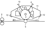
図2に、電子写真感光体1を備えたプロセスカートリッジ11を有する電子写真装置の概略構成の一例を示す。
円筒状(ドラム状)の電子写真感光体1は、軸2を中心に矢印方向に所定の周速度(プロセススピード)で回転駆動される。電子写真感光体1の表面は、回転過程において、帯電手段3により、正または負の所定電位に帯電される。なお、図2においては、ローラー型帯電部材によるローラー帯電方式を示しているが、コロナ帯電方式、近接帯電方式、注入帯電方式などの帯電方式を採用してもよい。帯電された電子写真感光体1の表面には、露光手段(不図示)から露光光4が照射され、目的の画像情報に対応した静電潜像が形成される。露光光4は、目的の画像情報の時系列電気デジタル画像信号に対応して強度変調された光であり、例えば、スリット露光やレーザービーム走査露光などの像露光手段から出力される。電子写真感光体1の表面に形成された静電潜像は、現像手段5内に収容されたトナーで現像(正規現像または反転現像)され、電子写真感光体1の表面にはトナー像が形成される。電子写真感光体1の表面に形成されたトナー像は、転写手段6により、転写材7に転写される。このとき、転写手段6には、バイアス電源(不図示)からトナーの保有電荷とは逆極性のバイアス電圧が印加される。また、転写材7が紙である場合、転写材7は給紙部(不図示)から取り出されて、電子写真感光体1と転写手段6との間に電子写真感光体1の回転と同期して給送される。電子写真感光体1からトナー像が転写された転写材7は、電子写真感光体1の表面から分離されて、定着手段8へ搬送され、トナー像の定着処理を受けることにより、画像形成物(プリント、コピー)として電子写真装置の外へプリントアウトされる。電子写真装置は、転写後の電子写真感光体1の表面に残ったトナーなどの付着物を除去するための、クリーニング手段9を有していてもよい。また、クリーニング手段を別途設けず、上記付着物を現像手段などで除去する、いわゆる、クリーナーレスシステムを用いてもよい。本発明においては、上記の電子写真感光体1、帯電手段3、現像手段5、およびクリーニング手段9などから選択される構成要素のうち、複数の構成要素を容器に納め、一体に支持してプロセスカートリッジ11を形成し、それを電子写真装置本体に対して着脱自在に構成できる。例えば以下のように構成する。帯電手段3、現像手段5およびクリーニング手段9から選択される少なくとも1つを、電子写真感光体1とともに一体に支持してカートリッジ化する。これを、電子写真装置本体のレールなどの案内手段12を用いて、電子写真装置本体に着脱自在なプロセスカートリッジ11とすることができる。電子写真装置は、電子写真感光体1の表面を、前露光手段(不図示)からの前露光光10により除電処理する除電機構を有していてもよい。また、本発明のプロセスカートリッジ11を電子写真装置本体に着脱するために、レールなどの案内手段12を設けてもよい。本発明の電子写真装置は、電子写真感光体1、ならびに、帯電手段3、露光手段、現像手段5および転写手段6からなる群より選択される少なくとも1つの手段を有することを特徴とする。
FIG. 2 shows an example of a schematic configuration of an electrophotographic apparatus having a
The cylindrical (drum-shaped) electrophotographic photosensitive member 1 is rotationally driven at a predetermined peripheral speed (process speed) in the direction of an arrow about a shaft 2. The surface of the electrophotographic photosensitive member 1 is charged to a predetermined positive or negative potential by the charging means 3 in the rotation process. Although FIG. 2 shows a roller charging method using a roller type charging member, a charging method such as a corona charging method, a proximity charging method, or an injection charging method may be adopted. The surface of the charged electrophotographic photosensitive member 1 is irradiated with exposure light 4 from an exposure means (not shown), and an electrostatic latent image corresponding to the target image information is formed. The exposure light 4 is intensity-modulated light corresponding to a time-series electric digital image signal of target image information, and is output from an image exposure means such as slit exposure or laser beam scanning exposure. The electrostatic latent image formed on the surface of the electrophotographic photosensitive member 1 is developed (regular development or reverse development) with the toner contained in the developing means 5, and a toner image is formed on the surface of the electrophotographic photosensitive member 1. Will be done. The toner image formed on the surface of the electrophotographic photosensitive member 1 is transferred to the transfer material 7 by the transfer means 6. At this time, a bias voltage having a polarity opposite to the charge held by the toner is applied to the transfer means 6 from a bias power supply (not shown). When the transfer material 7 is paper, the transfer material 7 is taken out from a paper feeding unit (not shown) and synchronizes with the rotation of the electrophotographic photosensitive member 1 between the electrophotographic photosensitive member 1 and the transfer means 6. Will be sent. The transfer material 7 to which the toner image is transferred from the electrophotographic photosensitive member 1 is separated from the surface of the electrophotographic photosensitive member 1, transported to the fixing means 8, and subjected to the fixing process of the toner image to form an image forming product ( It is printed out of the electrophotographic device as (print, copy). The electrophotographic apparatus may have a cleaning means 9 for removing deposits such as toner remaining on the surface of the electrophotographic photosensitive member 1 after transfer. Further, a so-called cleanerless system may be used in which the above-mentioned deposits are removed by a developing means or the like without separately providing a cleaning means. In the present invention, among the components selected from the electrophotographic photosensitive member 1, the charging means 3, the developing means 5, the cleaning means 9, and the like, a plurality of components are housed in a container and integrally supported for the process. The
本発明の電子写真感光体は、レーザービームプリンター、LEDプリンター、複写機、ファクシミリ、および、これらの複合機などに用いることができる。 The electrophotographic photosensitive member of the present invention can be used for laser beam printers, LED printers, copiers, facsimiles, and multifunction devices thereof.
以下、実施例および比較例を用いて本発明をさらに詳細に説明する。本発明は、その要旨を超えない限り、下記の実施例によって何ら限定されるものではない。なお、以下の実施例の記載において、「部」とあるのは特に断りのない限り質量基準である。 Hereinafter, the present invention will be described in more detail with reference to Examples and Comparative Examples. The present invention is not limited to the following examples as long as the gist of the present invention is not exceeded. In the description of the following examples, the term "part" is based on mass unless otherwise specified.
〔実施例1〕
・支持体
支持体(導電性支持体)として、円筒状アルミニウムシリンダー(JIS−A3003、アルミニウム合金、直径30mm、長さ357.5mm、肉厚1.0mm)を用いた。
[Example 1]
-Support As a support (conductive support), a cylindrical aluminum cylinder (JIS-A3003, aluminum alloy, diameter 30 mm, length 357.5 mm, wall thickness 1.0 mm) was used.
・下引き層の形成
ポリアミド樹脂(商品名:CM8000、東レ社製)1部をメタノール10部に溶解させた。この溶液に、酸化チタン粒子(商品名:SMT500SAS、テイカ社製)3部を加え、これを直径0.8mmのガラスビーズを用いたサンドミル装置で23±3℃雰囲気下で10時間分散し、下引き層用塗布液を調製した。
得られた下引き層用塗布液を前記支持体上に浸漬塗布して塗膜を形成し、塗膜を110℃で20分間乾燥させることによって、膜厚が2.0μmの下引き層を形成した。
-Formation of undercoat layer 1 part of polyamide resin (trade name: CM8000, manufactured by Toray Industries, Inc.) was dissolved in 10 parts of methanol. To this solution, 3 parts of titanium oxide particles (trade name: SMT500SAS, manufactured by TAYCA) were added, and this was dispersed in a sand mill device using glass beads having a diameter of 0.8 mm for 10 hours in an atmosphere of 23 ± 3 ° C. A coating solution for a pulling layer was prepared.
The obtained coating liquid for the undercoat layer is dipped and coated on the support to form a coating film, and the coating film is dried at 110 ° C. for 20 minutes to form an undercoat layer having a film thickness of 2.0 μm. did.
・電荷発生層の形成
α−クロロナフタレン100部中、o−フタロジニトリル5.0部、四塩化チタン2.0部を200℃にて3時間加熱攪拌した後、50℃まで冷却して析出した結晶を濾別してジクロロチタニウムフタロシアニンのペーストを得た。次に、これを100℃に加熱したN,N−ジメチルホルムアミド100部で攪拌洗浄し、次いで60℃のメタノール100部で2回洗浄を繰り返し濾別した。さらに、この得られたペーストを脱イオン水100部中80℃で1時間攪拌し、濾別して青色のチタニルフタロシアニン顔料を得た。次に、この顔料を濃硫酸30部に溶解させ20℃の脱イオン水300部中に攪拌下で滴下して再析出し、濾過して十分に水洗し、非晶質チタニルフタロシアニンを得た。
-Formation of charge generation layer Of 100 parts of α-chloronaphthalene, 5.0 parts of o-phthalocyanine and 2.0 parts of titanium tetrachloride were heated and stirred at 200 ° C. for 3 hours, then cooled to 50 ° C. and precipitated. The crystals were separated by filtration to obtain a dichlorotitanium phthalocyanine paste. Next, this was stirred and washed with 100 parts of N, N-dimethylformamide heated to 100 ° C., and then washed twice with 100 parts of methanol at 60 ° C. and filtered off repeatedly. Further, the obtained paste was stirred in 100 parts of deionized water at 80 ° C. for 1 hour and separated by filtration to obtain a blue titanyl phthalocyanine pigment. Next, this pigment was dissolved in 30 parts of concentrated sulfuric acid, dropped in 300 parts of deionized water at 20 ° C. under stirring, reprecipitated, filtered and thoroughly washed with water to obtain amorphous titanyl phthalocyanine.
α−クロロナフタレン150部に、上述の方法で得られた非晶質チタニルフタロシアニン8部、および2,3−ブタンジオール(東京化成工業(株)製)2.0部を混合し、温度180℃で6時間撹拌した。その後、室温まで冷却した後濾別し、メタノールで洗浄を繰り返し、減圧乾燥することにより、チタニルフタロシアニンと2,3−ブタンジオールの反応生成物である電荷発生物質G−1を得た。 To 150 parts of α-chloronaphthalene, 8 parts of amorphous titanylphthalocyanine obtained by the above method and 2.0 parts of 2,3-butanediol (manufactured by Tokyo Chemical Industry Co., Ltd.) are mixed, and the temperature is 180 ° C. Was stirred for 6 hours. Then, the mixture was cooled to room temperature, separated by filtration, washed with methanol repeatedly, and dried under reduced pressure to obtain a charge generating substance G-1 which is a reaction product of titanyl phthalocyanine and 2,3-butanediol.
電荷発生物質G−1は、マススペクトルにおいてm/Z=648にピークを示した。また、IRスペクトルにおいて630cm−1付近のO−Ti−O構造に由来すると考えられる吸収が見られた。以上のことから、電荷発生物質G−1が、2,3−ブタンジオール付加体チタニルフタロシアニンの単一結晶であると推定した。 The charge generator G-1 peaked at m / Z = 648 in the mass spectrum. In addition, in the IR spectrum, absorption considered to be derived from the O-Ti-O structure near 630 cm- 1 was observed. From the above, it was estimated that the charge generating substance G-1 is a single crystal of the 2,3-butanediol adduct titanyl phthalocyanine.
次に、電荷発生物質G−1を20部、ポリビニルブチラール樹脂(商品名:#6000−C、電気化学工業(株)製)10部、酢酸t−ブチル700部、4−メトキシ−4−メチル−2−ペンタノン300部を混合した。その後、直径1mmのガラスビーズを用いたサンドミルにて23±3℃の雰囲気下で10時間分散処理し、電荷発生層用塗布液を調製した。
この電荷発生層用塗布液を前記下引き層上に浸漬塗布し、得られた塗膜を10分間90℃で乾燥させることによって、膜厚が0.3μmの電荷発生層を形成した。
Next, 20 parts of the charge generating substance G-1, 10 parts of polyvinyl butyral resin (trade name: # 6000-C, manufactured by Denki Kagaku Kogyo Co., Ltd.), 700 parts of t-butyl acetate, 4-methoxy-4-methyl. -2-300 parts of pentanone was mixed. Then, a sand mill using glass beads having a diameter of 1 mm was subjected to dispersion treatment in an atmosphere of 23 ± 3 ° C. for 10 hours to prepare a coating liquid for a charge generation layer.
The coating liquid for the charge generating layer was immersed and coated on the undercoat layer, and the obtained coating film was dried at 90 ° C. for 10 minutes to form a charge generating layer having a film thickness of 0.3 μm.
・電荷輸送層の形成
次に、式(2−1)で示される化合物225部、ポリカーボネート樹脂(商品名:Z300、三菱ガス化学(株)製)300質量部、酸化防止剤(商品名:Irganox1010、日本チバガイギー(株)製)6部、シリコーンオイルKF−54(信越化学(株)製)1質量部を、テトラヒドロフラン1600質量部、およびトルエン400質量部の混合溶剤に溶解させることによって、電荷輸送層用塗布液を調製した。
この電荷輸送層用塗布液を前記電荷発生層上に浸漬塗布して塗膜を形成し、得られた塗膜を100℃で30分間乾燥させることによって、膜厚20μmの電荷輸送層を形成した。
-Formation of charge transport layer Next, 225 parts of the compound represented by the formula (2-1), 300 parts by mass of a polycarbonate resin (trade name: Z300, manufactured by Mitsubishi Gas Chemical Company, Inc.), an antioxidant (trade name: Irganox1010). , Nippon Ciba Geigy Co., Ltd.) 6 parts, silicone oil KF-54 (manufactured by Shinetsu Chemical Co., Ltd.) 1 part by mass is dissolved in a mixed solvent of 1600 parts by mass of tetrahydrofuran and 400 parts by mass of toluene to transport charges. A coating solution for layers was prepared.
The coating liquid for the charge transport layer was immersed and coated on the charge generation layer to form a coating film, and the obtained coating film was dried at 100 ° C. for 30 minutes to form a charge transport layer having a film thickness of 20 μm. ..
・表面層の形成
酸化スズ粒子(数平均一次粒径15nm)100質量部、シランカップリング剤(商品名:KBM−503、信越シリコーン(株)製)30質量部、メチルエチルケトン900質量部を湿式サンドミルに投入し、更に直径0.5mmのガラスビーズを加えて6時間の分散処理を行なった。その後、メチルエチルケトンとガラスビーズをろ別し、60℃の乾燥処理を行ないメタクリロイルオキシ基を有するシランカップリング剤で表面処理された酸化スズ粒子M1を得た。
-Formation of surface layer 100 parts by mass of tin oxide particles (number average primary particle size 15 nm), 30 parts by mass of silane coupling agent (trade name: KBM-503, manufactured by Shinetsu Silicone Co., Ltd.), 900 parts by mass of methyl ethyl ketone with a wet sand mill Further, glass beads having a diameter of 0.5 mm were added to carry out a dispersion treatment for 6 hours. Then, the methyl ethyl ketone and the glass beads were separated by filtration and dried at 60 ° C. to obtain tin oxide particles M1 surface-treated with a silane coupling agent having a methacryloyloxy group.
前記酸化スズ粒子M1を15部、式(1−1)で示される化合物60部、式(4−3)で示される化合物25部、重合開始剤(商品名:イルガキュア819、BASFジャパン社製)、2−ブタノール320部、テトラヒドロフラン40部を混合した。その後、直径0.5mmのガラスビーズを用いたサンドミルにて23±3℃の雰囲気下で6時間分散処理し、表面層用塗布液を調製した。
この表面層用塗布液を前記電荷輸送層上に浸漬塗布して塗膜を形成し、窒素雰囲気下にてメタルハライドランプを用いて、光源から感光体表面までの距離50mm、ランプ出力を4kWの条件で1分間紫外線を塗膜に照射した。得られた塗膜を80℃で70分間乾燥させ、膜厚7μmの表面層を形成した。
このようにして、電子写真感光体を作製した。
15 parts of the tin oxide particles M1, 60 parts of the compound represented by the formula (1-1), 25 parts of the compound represented by the formula (4-3), a polymerization initiator (trade name: Irgacure 819, manufactured by BASF Japan Ltd.). , 320 parts of 2-butanol and 40 parts of tetrahydrofuran were mixed. Then, the coating liquid for the surface layer was prepared by dispersion treatment for 6 hours in an atmosphere of 23 ± 3 ° C. in a sand mill using glass beads having a diameter of 0.5 mm.
The coating liquid for the surface layer is immersed and coated on the charge transport layer to form a coating film, and a metal halide lamp is used in a nitrogen atmosphere to obtain a distance of 50 mm from the light source to the surface of the photoconductor and a lamp output of 4 kW. The coating film was irradiated with ultraviolet rays for 1 minute. The obtained coating film was dried at 80 ° C. for 70 minutes to form a surface layer having a film thickness of 7 μm.
In this way, an electrophotographic photosensitive member was produced.
〔実施例2〕
シランカップリング剤(商品名:KBM−503、信越シリコーン(株)製)をシランカップリング剤(商品名:KBM−5103、信越シリコーン(株)製)に変更したこと以外は、実施例1と同様にして、電子写真感光体を作製した。
[Example 2]
Example 1 and Example 1 except that the silane coupling agent (trade name: KBM-503, manufactured by Shinetsu Silicone Co., Ltd.) was changed to the silane coupling agent (trade name: KBM-5103, manufactured by Shinetsu Silicone Co., Ltd.). In the same manner, an electrophotographic photosensitive member was prepared.
〔実施例3〕
酸化スズ粒子(数平均一次粒径15nm)を酸化チタン粒子(商品名:CR−EL、ルチル化率:99.1%、石原産業株式会社製)に変更したこと以外は、実施例1と同様にして、電子写真感光体を作製した。
[Example 3]
Same as Example 1 except that tin oxide particles (number average primary particle size 15 nm) were changed to titanium oxide particles (trade name: CR-EL, rutile conversion rate: 99.1%, manufactured by Ishihara Sangyo Co., Ltd.). To prepare an electrophotographic photosensitive member.
〔実施例4〕
式(2−1)で示される化合物を式(2−2)で示される化合物に変更したこと以外は、実施例1と同様にして、電子写真感光体を作製した。
[Example 4]
An electrophotographic photosensitive member was produced in the same manner as in Example 1 except that the compound represented by the formula (2-1) was changed to the compound represented by the formula (2-2).
〔実施例5〕
α−クロロナフタレン150部に、実施例1に記載の方法で得られた非晶質チタニルフタロシアニン8部、および2,3−ブタンジオール(東京化成工業(株)製)0.75部を混合し、温度60℃で6時間撹拌した。その後、室温まで冷却した後濾別し、メタノールで洗浄を繰り返し、減圧乾燥することにより、チタニルフタロシアニンと2,3−ブタンジオールの反応生成物である電荷発生物質G−2を得た。
電荷発生物質G−2は、マススペクトルにおいてm/Z=576、および648にピークを示した。また、IRスペクトルにおいて970cm−1付近のTi=O構造に由来すると考えられる吸収、および630cm−1付近のO−Ti−O構造に由来すると考えられる吸収が見られた。以上のことから、電荷発生物質G−2が、2,3−ブタンジオール付加体チタニルフタロシアニンと、未付加体チタニルフタロシアニンの混晶であると推定した。
[Example 5]
To 150 parts of α-chloronaphthalene, 8 parts of amorphous titanylphthalocyanine obtained by the method described in Example 1 and 0.75 parts of 2,3-butanediol (manufactured by Tokyo Chemical Industry Co., Ltd.) are mixed. , Stirred at a temperature of 60 ° C. for 6 hours. Then, the mixture was cooled to room temperature, separated by filtration, washed with methanol repeatedly, and dried under reduced pressure to obtain a charge generating substance G-2 which is a reaction product of titanyl phthalocyanine and 2,3-butanediol.
The charge generator G-2 peaked at m / Z = 576 and 648 in the mass spectrum. Moreover, absorption is considered to be derived from Ti = O structure in the vicinity of 970 cm -1 in the IR spectrum, and absorption believed to originate from the O-Ti-O structure of 630cm around -1 was observed. From the above, it was estimated that the charge generating substance G-2 is a mixed crystal of 2,3-butanediol adduct titanyl phthalocyanine and non-adducted titanyl phthalocyanine.
電荷発生物質G−1を電荷発生物質G−2に変更して電荷発生層用塗布液を調製したこと以外は、実施例1と同様にして、電子写真感光体を作製した。 An electrophotographic photosensitive member was produced in the same manner as in Example 1 except that the charge generating substance G-1 was changed to the charge generating substance G-2 to prepare a coating liquid for the charge generating layer.
〔実施例6〕
式(4−3)で示される化合物を式(4−4)で示される化合物に変更したこと以外は、実施例1と同様にして、電子写真感光体を作製した。
[Example 6]
An electrophotographic photosensitive member was produced in the same manner as in Example 1 except that the compound represented by the formula (4-3) was changed to the compound represented by the formula (4-4).
〔実施例7〕
式(1−1)で示される化合物を式(1−3)で示される化合物に変更して表面層用塗布液を調製したこと以外は、実施例1と同様にして、電子写真感光体を作製した。
[Example 7]
The electrophotographic photosensitive member was prepared in the same manner as in Example 1 except that the compound represented by the formula (1-1) was changed to the compound represented by the formula (1-3) to prepare a coating liquid for the surface layer. Made.
〔実施例8〕
以下のように、表面層用塗布液を調製したこと以外は、実施例1と同様にして電子写真感光体を作製した。
前記酸化スズ粒子M1を15部、下記式(7)で示される化合物15部、式(1−1)で示される化合物60部、式(4−3)で示される化合物10部、重合開始剤(商品名:イルガキュア819、BASFジャパン社製)、2−ブタノール320部、テトラヒドロフラン40部を混合した。その後、直径0.5mmのガラスビーズを用いたサンドミルにて23±3℃の雰囲気下で6時間分散処理し、表面層用塗布液を調製した。
An electrophotographic photosensitive member was prepared in the same manner as in Example 1 except that the coating liquid for the surface layer was prepared as described below.
15 parts of the tin oxide particles M1, 15 parts of the compound represented by the following formula (7), 60 parts of the compound represented by the formula (1-1), 10 parts of the compound represented by the formula (4-3), a polymerization initiator. (Product name: Irgacure 819, manufactured by BASF Japan Ltd.), 320 parts of 2-butanol and 40 parts of tetrahydrofuran were mixed. Then, the coating liquid for the surface layer was prepared by dispersion treatment for 6 hours in an atmosphere of 23 ± 3 ° C. in a sand mill using glass beads having a diameter of 0.5 mm.
〔実施例9〕
式(7)で示される化合物を下記式(8)で示される化合物に変更して表面層用塗布液を調製したこと以外は、実施例8と同様にして、電子写真感光体を作製した。
An electrophotographic photosensitive member was produced in the same manner as in Example 8 except that the compound represented by the formula (7) was changed to the compound represented by the following formula (8) to prepare a coating liquid for the surface layer.
〔実施例10〕
以下のように、表面層用塗布液を調製したこと以外は、実施例1と同様にして電子写真感光体を作製した。
前記酸化スズ粒子M1を15部、式(1−1)で示される化合物35部、式(5−1)で示される化合物25部、式(4−3)で示される化合物25部、重合開始剤(商品名:イルガキュア819、BASFジャパン社製)、2−ブタノール320部、テトラヒドロフラン40部を混合した。その後、直径0.5mmのガラスビーズを用いたサンドミルにて23±3℃の雰囲気下で6時間分散処理し、表面層用塗布液を調製した。
[Example 10]
An electrophotographic photosensitive member was prepared in the same manner as in Example 1 except that the coating liquid for the surface layer was prepared as described below.
15 parts of the tin oxide particles M1, 35 parts of the compound represented by the formula (1-1), 25 parts of the compound represented by the formula (5-1), 25 parts of the compound represented by the formula (4-3), polymerization initiation. The agent (trade name: Irgacure 819, manufactured by BASF Japan Ltd.), 320 parts of 2-butanol, and 40 parts of tetrahydrofuran were mixed. Then, the coating liquid for the surface layer was prepared by dispersion treatment for 6 hours in an atmosphere of 23 ± 3 ° C. in a sand mill using glass beads having a diameter of 0.5 mm.
〔実施例11〕
以下のように、表面層用塗布液を調製したこと以外は、実施例1と同様にして電子写真感光体を作製した。
前記酸化スズ粒子M1を12部、式(1−1)で示される化合物15部、式(4−3)で示される化合物25部、重合開始剤(商品名:イルガキュア819、BASFジャパン社製)、2−ブタノール320部、テトラヒドロフラン40部を混合した。その後、直径0.5mmのガラスビーズを用いたサンドミルにて23±3℃の雰囲気下で6時間分散処理し、表面層用塗布液を調製した。
[Example 11]
An electrophotographic photosensitive member was prepared in the same manner as in Example 1 except that the coating liquid for the surface layer was prepared as described below.
12 parts of the tin oxide particles M1, 15 parts of the compound represented by the formula (1-1), 25 parts of the compound represented by the formula (4-3), a polymerization initiator (trade name: Irgacure 819, manufactured by BASF Japan Ltd.). , 320 parts of 2-butanol and 40 parts of tetrahydrofuran were mixed. Then, the coating liquid for the surface layer was prepared by dispersion treatment for 6 hours in an atmosphere of 23 ± 3 ° C. in a sand mill using glass beads having a diameter of 0.5 mm.
〔実施例12〕
以下のように、表面層用塗布液を調製したこと以外は、実施例1と同様にして電子写真感光体を作製した。
前記酸化スズ粒子M1を1.4部、式(1−1)で示される化合物60部、式(4−3)で示される化合物25部、重合開始剤(商品名:イルガキュア819、BASFジャパン社製)、2−ブタノール320部、テトラヒドロフラン40部を混合した。その後、直径0.5mmのガラスビーズを用いたサンドミルにて23±3℃の雰囲気下で6時間分散処理し、表面層用塗布液を調製した。
[Example 12]
An electrophotographic photosensitive member was prepared in the same manner as in Example 1 except that the coating liquid for the surface layer was prepared as described below.
1.4 parts of the tin oxide particles M1, 60 parts of the compound represented by the formula (1-1), 25 parts of the compound represented by the formula (4-3), a polymerization initiator (trade name: Irgacure 819, BASF Japan Ltd.) , 2-butanol (320 parts) and tetrahydrofuran (40 parts) were mixed. Then, the coating liquid for the surface layer was prepared by dispersion treatment for 6 hours in an atmosphere of 23 ± 3 ° C. in a sand mill using glass beads having a diameter of 0.5 mm.
〔実施例13〕
以下のように、表面層用塗布液を調製したこと以外は、実施例1と同様にして電子写真感光体を作製した。
前記酸化スズ粒子M1を15部、式(1−1)で示される化合物10部、式(4−3)で示される化合物25部、重合開始剤(商品名:イルガキュア819、BASFジャパン社製)、2−ブタノール320部、テトラヒドロフラン40部を混合した。その後、直径0.5mmのガラスビーズを用いたサンドミルにて23±3℃の雰囲気下で6時間分散処理し、表面層用塗布液を調製した。
[Example 13]
An electrophotographic photosensitive member was prepared in the same manner as in Example 1 except that the coating liquid for the surface layer was prepared as described below.
15 parts of the tin oxide particles M1, 10 parts of the compound represented by the formula (1-1), 25 parts of the compound represented by the formula (4-3), a polymerization initiator (trade name: Irgacure 819, manufactured by BASF Japan Ltd.). , 320 parts of 2-butanol and 40 parts of tetrahydrofuran were mixed. Then, the coating liquid for the surface layer was prepared by dispersion treatment for 6 hours in an atmosphere of 23 ± 3 ° C. in a sand mill using glass beads having a diameter of 0.5 mm.
〔実施例14〕
以下のように、表面層用塗布液を調製したこと以外は、実施例1と同様にして電子写真感光体を作製した。
前記酸化スズ粒子M1を1.3部、式(1−1)で示される化合物60部、式(4−3)で示される化合物25部、重合開始剤(商品名:イルガキュア819、BASFジャパン社製)、2−ブタノール320部、テトラヒドロフラン40部を混合した。その後、直径0.5mmのガラスビーズを用いたサンドミルにて23±3℃の雰囲気下で6時間分散処理し、表面層用塗布液を調製した。
[Example 14]
An electrophotographic photosensitive member was prepared in the same manner as in Example 1 except that the coating liquid for the surface layer was prepared as described below.
1.3 parts of the tin oxide particles M1, 60 parts of the compound represented by the formula (1-1), 25 parts of the compound represented by the formula (4-3), a polymerization initiator (trade name: Irgacure 819, BASF Japan Ltd.) , 2-butanol (320 parts) and tetrahydrofuran (40 parts) were mixed. Then, the coating liquid for the surface layer was prepared by dispersion treatment for 6 hours in an atmosphere of 23 ± 3 ° C. in a sand mill using glass beads having a diameter of 0.5 mm.
〔実施例15〕
シランカップリング剤(商品名:KBM−503、信越シリコーン(株)製)をシランカップリング剤(商品名:KBM−1003、信越シリコーン(株)製)に変更したこと以外は、実施例1と同様にして、電子写真感光体を作製した。
[Example 15]
Example 1 and Example 1 except that the silane coupling agent (trade name: KBM-503, manufactured by Shinetsu Silicone Co., Ltd.) was changed to the silane coupling agent (trade name: KBM-1003, manufactured by Shinetsu Silicone Co., Ltd.). In the same manner, an electrophotographic photosensitive member was prepared.
〔実施例16〕
酸化スズ粒子(数平均一次粒径15nm)をα−アルミナ(商品名:スミコランダムAA−03、住友化学工業社製)に変更したこと以外は、実施例1と同様にして、電子写真感光体を作製した。
[Example 16]
Electrophotographic photosensitive member in the same manner as in Example 1 except that tin oxide particles (number average primary particle size 15 nm) were changed to α-alumina (trade name: Sumiko Random AA-03, manufactured by Sumitomo Chemical Co., Ltd.). Was produced.
〔実施例17〕
式(2−1)で示される化合物を前記式(4−7)で示される化合物に変更したこと以外は、実施例1と同様にして、電子写真感光体を作製した。
[Example 17]
An electrophotographic photosensitive member was produced in the same manner as in Example 1 except that the compound represented by the formula (2-1) was changed to the compound represented by the formula (4-7).
〔実施例18〕
以下のように、電荷発生層用塗布液を調製したこと以外は、実施例1と同様にして電子写真感光体を作製した。
CuKα特性X線回折におけるブラッグ角2θ±0.2°の7.4°および28.1°に強いピークを有する結晶形のヒドロキシガリウムフタロシアニン結晶(電荷発生物質)4部、および、下記構造式(9)で示される化合物0.04部を、シクロヘキサノン100部にポリビニルブチラール(商品名:エスレックBX−1、積水化学工業(株)製)2部を溶解させた液に加えた。その後、直径1mmのガラスビーズを用いたサンドミルにて23±3℃の雰囲気下で1時間分散処理し、分散処理後、酢酸エチル100部を加えることによって、電荷発生層用塗布液を調製した。
An electrophotographic photosensitive member was produced in the same manner as in Example 1 except that the coating liquid for the charge generation layer was prepared as described below.
4 parts of crystalline hydroxygallium phthalocyanine crystal (charge generator) having strong peaks at 7.4 ° and 28.1 ° of Bragg angle 2θ ± 0.2 ° in CuKα characteristic X-ray diffraction, and the following structural formula ( 0.04 part of the compound shown in 9) was added to a solution prepared by dissolving 2 parts of polyvinyl butyral (trade name: Eslek BX-1, manufactured by Sekisui Chemical Industry Co., Ltd.) in 100 parts of cyclohexanone. Then, the dispersion treatment was carried out in a sand mill using glass beads having a diameter of 1 mm for 1 hour in an atmosphere of 23 ± 3 ° C., and after the dispersion treatment, 100 parts of ethyl acetate was added to prepare a coating liquid for a charge generation layer.
〔実施例19〕
式(4−3)で示される化合物を下記式(10)で示される化合物に変更したこと以外は、実施例1と同様にして、電子写真感光体を作製した。
An electrophotographic photosensitive member was produced in the same manner as in Example 1 except that the compound represented by the formula (4-3) was changed to the compound represented by the following formula (10).
〔実施例20〕
式(1−1)で示される化合物を、式(1−5)で示される化合物に変更して表面層用塗布液を調製したこと以外は、実施例1と同様にして、電子写真感光体を作製した。
[Example 20]
An electrophotographic photosensitive member in the same manner as in Example 1 except that the compound represented by the formula (1-1) was changed to the compound represented by the formula (1-5) to prepare a coating liquid for the surface layer. Was produced.
〔実施例21〕
式(1−1)で示される化合物を、式(1−6)で示される化合物に変更して表面層用塗布液を調製したこと以外は、実施例1と同様にして、電子写真感光体を作製した。
[Example 21]
An electrophotographic photosensitive member in the same manner as in Example 1 except that the compound represented by the formula (1-1) was changed to the compound represented by the formula (1-6) to prepare a coating liquid for the surface layer. Was produced.
〔実施例22〕
式(4−3)で示される化合物を前記式(10)で示される化合物に変更したこと以外は、実施例21と同様にして、電子写真感光体を作製した。
[Example 22]
An electrophotographic photosensitive member was produced in the same manner as in Example 21 except that the compound represented by the formula (4-3) was changed to the compound represented by the formula (10).
〔実施例23〕
以下のように、電荷発生層用塗布液を調製したこと以外は、実施例22と同様にして電子写真感光体を作製した。
CuKα特性X線回折におけるブラッグ角2θ±0.2°の7.4°および28.1°に強いピークを有する結晶形のヒドロキシガリウムフタロシアニン結晶(電荷発生物質)4部、および、前記構造式(10)で示される化合物0.04部を、シクロヘキサノン100部にポリビニルブチラール(商品名:エスレックBX−1、積水化学工業(株)製)2部を溶解させた液に加えた。その後、直径1mmのガラスビーズを用いたサンドミルにて23±3℃の雰囲気下で1時間分散処理し、分散処理後、酢酸エチル100部を加えることによって、電荷発生層用塗布液を調製した。
[Example 23]
An electrophotographic photosensitive member was produced in the same manner as in Example 22 except that the coating liquid for the charge generation layer was prepared as described below.
4 parts of crystalline hydroxygallium phthalocyanine crystal (charge generator) having strong peaks at 7.4 ° and 28.1 ° of Bragg angle 2θ ± 0.2 ° in CuKα characteristic X-ray diffraction, and the above structural formula ( 0.04 part of the compound represented by 10) was added to a solution prepared by dissolving 2 parts of polyvinyl butyral (trade name: Eslek BX-1, manufactured by Sekisui Chemical Industry Co., Ltd.) in 100 parts of cyclohexanone. Then, the dispersion treatment was carried out in a sand mill using glass beads having a diameter of 1 mm for 1 hour in an atmosphere of 23 ± 3 ° C., and after the dispersion treatment, 100 parts of ethyl acetate was added to prepare a coating liquid for a charge generation layer.
〔実施例24〕
式(2−1)で示される化合物を前記式(9)で示される化合物に変更したこと以外は、実施例23と同様にして、電子写真感光体を作製した。
[Example 24]
An electrophotographic photosensitive member was produced in the same manner as in Example 23, except that the compound represented by the formula (2-1) was changed to the compound represented by the formula (9).
〔実施例25〕
酸化スズ粒子(数平均一次粒径15nm)をα−アルミナ(商品名:スミコランダムAA−03、住友化学工業社製)に変更したこと以外は、実施例24と同様にして、電子写真感光体を作製した。
[Example 25]
Electrophotographic photosensitive member in the same manner as in Example 24, except that tin oxide particles (number average primary particle size 15 nm) were changed to α-alumina (trade name: Sumiko Random AA-03, manufactured by Sumitomo Chemical Co., Ltd.). Was produced.
〔実施例26〕
シランカップリング剤(商品名:KBM−503、信越シリコーン(株)製)をシランカップリング剤(商品名:KBM−1003、信越シリコーン(株)製)に変更したこと以外は、実施例25と同様にして、電子写真感光体を作製した。
[Example 26]
Example 25 and Example 25 except that the silane coupling agent (trade name: KBM-503, manufactured by Shin-Etsu Silicone Co., Ltd.) was changed to the silane coupling agent (trade name: KBM-1003, manufactured by Shin-Etsu Silicone Co., Ltd.). In the same manner, an electrophotographic photosensitive member was prepared.
〔実施例27〕
以下のように、表面層用塗布液を調製したこと以外は、実施例26と同様にして電子写真感光体を作製した。
前記酸化スズ粒子M1を15部、式(1−1)で示される化合物10部、式(4−3)で示される化合物25部、重合開始剤(商品名:イルガキュア819、BASFジャパン社製)、2−ブタノール320部、テトラヒドロフラン40部を混合した。その後、直径0.5mmのガラスビーズを用いたサンドミルにて23±3℃の雰囲気下で6時間分散処理し、表面層用塗布液を調製した。
[Example 27]
An electrophotographic photosensitive member was produced in the same manner as in Example 26 except that the coating liquid for the surface layer was prepared as described below.
15 parts of the tin oxide particles M1, 10 parts of the compound represented by the formula (1-1), 25 parts of the compound represented by the formula (4-3), a polymerization initiator (trade name: Irgacure 819, manufactured by BASF Japan Ltd.). , 320 parts of 2-butanol and 40 parts of tetrahydrofuran were mixed. Then, the coating liquid for the surface layer was prepared by dispersion treatment for 6 hours in an atmosphere of 23 ± 3 ° C. in a sand mill using glass beads having a diameter of 0.5 mm.
〔実施例28〕
以下のように、表面層用塗布液を調製したこと以外は、実施例26と同様にして電子写真感光体を作製した。
前記酸化スズ粒子M1を1.3部、式(1−1)で示される化合物60部、式(4−3)で示される化合物25部、重合開始剤(商品名:イルガキュア819、BASFジャパン社製)、2−ブタノール320部、テトラヒドロフラン40部を混合した。その後、直径0.5mmのガラスビーズを用いたサンドミルにて23±3℃の雰囲気下で6時間分散処理し、表面層用塗布液を調製した。
[Example 28]
An electrophotographic photosensitive member was produced in the same manner as in Example 26 except that the coating liquid for the surface layer was prepared as described below.
1.3 parts of the tin oxide particles M1, 60 parts of the compound represented by the formula (1-1), 25 parts of the compound represented by the formula (4-3), a polymerization initiator (trade name: Irgacure 819, BASF Japan Ltd.) , 2-butanol (320 parts) and tetrahydrofuran (40 parts) were mixed. Then, the coating liquid for the surface layer was prepared by dispersion treatment for 6 hours in an atmosphere of 23 ± 3 ° C. in a sand mill using glass beads having a diameter of 0.5 mm.
〔比較例1〕
式(1−1)で示される化合物を用いなかったこと以外は、実施例6と同様にして、電子写真感光体を作製した。
[Comparative Example 1]
An electrophotographic photosensitive member was prepared in the same manner as in Example 6 except that the compound represented by the formula (1-1) was not used.
〔比較例2〕
式(1−1)で示される化合物を用いなかったこと以外は、実施例10と同様にして、電子写真感光体を作製した。
[Comparative Example 2]
An electrophotographic photosensitive member was prepared in the same manner as in Example 10 except that the compound represented by the formula (1-1) was not used.
〔比較例3〕
式(1−1)で示される化合物を用いなかったこと以外は、実施例5と同様にして、電子写真感光体を作製した。
[Comparative Example 3]
An electrophotographic photosensitive member was prepared in the same manner as in Example 5 except that the compound represented by the formula (1-1) was not used.
<電子写真感光体の評価>
実施例1〜28および比較例1〜3に記載の方法で作製した電子写真感光体について、以下に示す方法で初期感度の評価および画像流れの評価を行った。
<Evaluation of electrophotographic photosensitive member>
The electrophotographic photosensitive members produced by the methods described in Examples 1 to 28 and Comparative Examples 1 to 3 were evaluated for initial sensitivity and image flow by the methods shown below.
・初期感度の評価
初期感度は、以下の方法で行った。感光体試験装置(商品名:CYNTHIA59、ジェンテック(株)製)を用いて、常温常湿(23℃/50%RH)環境下、高温高湿(30℃/85%RH)環境下それぞれにおいて、電子写真感光体の表面が−700Vになるように帯電装置の条件を設定した。これに波長780nmの単色光を照射して−700Vの電位を−200Vまで下げるのに必要な光量を測定し、感度(μJ/cm2)とした。
得られた感度について、以下の基準でレベルを評価した。本発明において、ランクAおよびBは初期感度が十分に得られており、ランクCは初期感度が不十分であると判断した。
ランクA:0.25μJ/cm2以上0.30μJ/cm2未満
ランクB:0.30μJ/cm2以上0.35μJ/cm2未満
ランクC:0.35μJ/cm2以上
このようにして評価した結果を表2に示す。
-Evaluation of initial sensitivity The initial sensitivity was performed by the following method. Using a photoconductor tester (trade name: CYNTHIA59, manufactured by Gentech Co., Ltd.) in a normal temperature and humidity (23 ° C / 50% RH) environment and a high temperature and high humidity (30 ° C / 85% RH) environment, respectively. , The conditions of the charging device were set so that the surface of the electrophotographic photosensitive member was -700 V. This was irradiated with monochromatic light having a wavelength of 780 nm, and the amount of light required to lower the potential of -700 V to -200 V was measured and used as the sensitivity (μJ / cm 2 ).
The level of the obtained sensitivity was evaluated according to the following criteria. In the present invention, it was determined that ranks A and B had sufficient initial sensitivity, and rank C had insufficient initial sensitivity.
Rank A: 0.25 μJ / cm 2 or more and less than 0.30 μJ / cm 2 Rank B: 0.30 μJ / cm 2 or more and less than 0.35 μJ / cm 2 Rank C: 0.35 μJ / cm 2 or more Evaluated in this way. The results are shown in Table 2.
・画像流れの評価
画像評価は、以下の方法で行った。まず帯電工程の総放電電流量を70μAに設定し、装置内のカセットヒーター(ドラムヒーター)をオフにした。その後、画像比率5%のテストチャートを用いて10万枚連続の画像形成を行った。画像形成終了後、複写機への給電を停止し、3日間放置した。3日間放置後に複写機に再び給電を開始し、A4横サイズ紙にて、格子画像および平仮名の「いろは」が繰り返された文字画像(いろは画像)を出力した。
得られたA4全面の画像について、以下の基準で画像流れレベルを評価した。本発明において、ランクAおよびBは画像流れの抑制効果が十分に得られており、ランクCは画像流れの抑制効果が得られていると判断した。ランクDは画像流れの抑制効果が得られていないと判断した。
ランクA:格子画像、いろは画像共に画像欠陥が見られない
ランクB:格子画像が一部かすんでおり、いろは画像が一部薄くなる
ランクC:格子画像が部分的に消失しており、いろは画像が全面薄くなる
ランクD:格子画像が全面消失しており、いろは画像が全面薄くなる
このようにして、以下に示す評価装置1および2を用いて画像流れを評価した結果を表2に示す。
-Evaluation of image flow Image evaluation was performed by the following method. First, the total discharge current amount in the charging process was set to 70 μA, and the cassette heater (drum heater) in the apparatus was turned off. Then, 100,000 continuous images were formed using a test chart having an image ratio of 5%. After the image formation was completed, the power supply to the copying machine was stopped and left for 3 days. After leaving it for 3 days, the power supply to the copier was started again, and a grid image and a character image (Iroha image) in which the hiragana "Iroha" was repeated were output on A4 horizontal size paper.
The image flow level of the obtained image of the entire surface of A4 was evaluated according to the following criteria. In the present invention, it was determined that ranks A and B sufficiently obtained the effect of suppressing image flow, and rank C obtained the effect of suppressing image flow. Rank D determined that the effect of suppressing image flow was not obtained.
Rank A: No image defects are seen in both the lattice image and the Iroha image Rank B: The lattice image is partially hazy and the Iroha image is partially faint Rank C: The lattice image is partially lost and the Iroha image Rank D: The lattice image is completely lost, and the Iroha image is completely thin. Table 2 shows the results of evaluating the image flow using the evaluation devices 1 and 2 shown below.
〔評価装置1〕
実施例1〜28および比較例1〜3において作製した電子写真感光体を、キヤノン(株)製の複写機imageRUNNER(iR)(登録商標)−ADV C5051の改造機(帯電手段は直流電圧に交流電圧を重畳した電圧をローラー型の接触帯電部材(帯電ローラー)を電子写真感光体に当接して印加する方式、露光手段はレーザー像露光方式(波長780nm))に装着して評価を行った。
詳しくは、高温高湿(30℃/85%RH)環境下に上記評価装置を設置した。シアン色用のプロセスカートリッジに、作製した電子写真感光体を装着して、シアンのプロセスカートリッジのステーションに装着し、画像流れの評価を行った。
[Evaluation device 1]
The electrophotographic photosensitive members produced in Examples 1 to 28 and Comparative Examples 1 to 3 were used with a modified machine of Canon ImageRUNNER (iR) (registered trademark) -ADV C5051 (charging means is AC to DC voltage). Evaluation was performed by mounting a voltage on which a voltage was superimposed on a roller-type contact charging member (charging roller) in contact with an electrophotographic photosensitive member and applying the voltage, and an exposure means using a laser image exposure method (wavelength 780 nm).
Specifically, the evaluation device was installed in a high temperature and high humidity (30 ° C./85% RH) environment. The prepared electrophotographic photosensitive member was attached to the cyan process cartridge and attached to the cyan process cartridge station to evaluate the image flow.
〔評価装置2〕
実施例1〜28および比較例1〜3において作製した電子写真感光体を、キヤノン(株)製の複写機iR−ADV C5051の改造機(帯電手段は直流電圧をローラー型の接触帯電部材(帯電ローラー)に印加する方式、露光手段はレーザー像露光方式(波長780nm))に装着して評価を行った。
詳しくは、高温高湿(30℃/85%RH)環境下に上記評価装置を設置した。シアン色用のプロセスカートリッジに、作製した電子写真感光体を装着して、シアンのプロセスカートリッジのステーションに装着し、画像流れの評価を行った。
[Evaluation device 2]
The electrophotographic photosensitive members produced in Examples 1 to 28 and Comparative Examples 1 to 3 were used as a modified machine of a copying machine iR-ADV C5051 manufactured by Canon Inc. (the charging means is a roller-type contact charging member (charging) with a DC voltage. The method applied to the roller) and the exposure means were attached to a laser image exposure method (wavelength 780 nm)) for evaluation.
Specifically, the evaluation device was installed in a high temperature and high humidity (30 ° C./85% RH) environment. The prepared electrophotographic photosensitive member was attached to the cyan process cartridge and attached to the cyan process cartridge station to evaluate the image flow.
表2に示す通り、本発明の電子写真感光体、ならびに本発明の電子写真感光体を用いたプロセスカートリッジおよび電子写真装置であれば、画像流れの発生の抑制について良好な結果が得られることが分かる。比較例のように、表面層が式(1)で示される化合物を含有しない場合には、画像流れが発生しやすいため、本発明の目的を達成できないことが分かる。 As shown in Table 2, the electrophotographic photosensitive member of the present invention, and the process cartridge and electrophotographic apparatus using the electrophotographic photosensitive member of the present invention, can obtain good results in suppressing the occurrence of image flow. I understand. It can be seen that when the surface layer does not contain the compound represented by the formula (1) as in the comparative example, image flow is likely to occur, so that the object of the present invention cannot be achieved.
21 支持体
22 下引き層
23 電荷発生層
24 電荷輸送層
25 表面層
1 電子写真感光体
2 軸
3 帯電手段
4 露光光
5 現像手段
6 転写手段
7 転写材
8 定着手段
9 クリーニング手段
10 前露光光
11 プロセスカートリッジ
12 案内手段
21 Support 22
Claims (10)
該表面層が、重合性化合物と、重合性官能基を表面に有する金属酸化物粒子とを含有する組成物の共重合物
を含有し、
前記重合性化合物が、下記式(1)で示される化合物を含有する
ことを特徴とする電子写真感光体。
The surface layer contains a copolymer of a composition containing a polymerizable compound and metal oxide particles having a polymerizable functional group on the surface.
An electrophotographic photosensitive member, wherein the polymerizable compound contains a compound represented by the following formula (1).
1≦Mα/Mβ≦45 (A)
を満たすことを特徴とする、請求項1に記載の電子写真感光体。 When the content of the compound represented by the formula (1) in the surface layer is M α and the content of the metal oxide particles having the polymerizable functional group on the surface is M β , the mass ratio is M α. / M β is the following formula (A)
1 ≤ M α / M β ≤ 45 (A)
The electrophotographic photosensitive member according to claim 1, wherein the electrophotographic photosensitive member satisfies the above conditions.
帯電手段、現像手段、および、クリーニング手段からなる群より選択される少なくとも1つの手段とを一体に支持し、
電子写真装置本体に着脱自在であるプロセスカートリッジ。 The electrophotographic photosensitive member according to any one of claims 1 to 8.
It integrally supports at least one means selected from the group consisting of charging means, developing means, and cleaning means.
A process cartridge that can be attached to and detached from the main body of the electrophotographic device.
帯電手段、露光手段、現像手段、および、転写手段からなる群より選択される少なくとも1つの手段とを有する電子写真装置。 The electrophotographic photosensitive member according to any one of claims 1 to 8.
An electrophotographic apparatus having at least one means selected from the group consisting of charging means, exposure means, developing means, and transfer means.
Priority Applications (2)
| Application Number | Priority Date | Filing Date | Title |
|---|---|---|---|
| JP2019110644A JP2020201467A (en) | 2019-06-13 | 2019-06-13 | Electro-photographic photoreceptor, process cartridge, and electro-photographic apparatus |
| US16/894,988 US11169453B2 (en) | 2019-06-13 | 2020-06-08 | Electrophotographic photosensitive member, process cartridge and electrophotographic apparatus |
Applications Claiming Priority (1)
| Application Number | Priority Date | Filing Date | Title |
|---|---|---|---|
| JP2019110644A JP2020201467A (en) | 2019-06-13 | 2019-06-13 | Electro-photographic photoreceptor, process cartridge, and electro-photographic apparatus |
Publications (2)
| Publication Number | Publication Date |
|---|---|
| JP2020201467A true JP2020201467A (en) | 2020-12-17 |
| JP2020201467A5 JP2020201467A5 (en) | 2022-06-07 |
Family
ID=73743978
Family Applications (1)
| Application Number | Title | Priority Date | Filing Date |
|---|---|---|---|
| JP2019110644A Pending JP2020201467A (en) | 2019-06-13 | 2019-06-13 | Electro-photographic photoreceptor, process cartridge, and electro-photographic apparatus |
Country Status (2)
| Country | Link |
|---|---|
| US (1) | US11169453B2 (en) |
| JP (1) | JP2020201467A (en) |
Families Citing this family (3)
| Publication number | Priority date | Publication date | Assignee | Title |
|---|---|---|---|---|
| JP7346243B2 (en) | 2019-10-29 | 2023-09-19 | キヤノン株式会社 | Electrophotographic photoreceptor, process cartridge, electrophotographic image forming apparatus, and method for manufacturing electrophotographic photoreceptor |
| US20230115474A1 (en) * | 2021-10-08 | 2023-04-13 | Canon Kabushiki Kaisha | Electrophotographic photosensitive member, process cartridge, and electrophotographic apparatus |
| JP2023074422A (en) | 2021-11-17 | 2023-05-29 | キヤノン株式会社 | Electrophotographic photoreceptor, process cartridge, and electrophotographic image forming apparatus |
Citations (3)
| Publication number | Priority date | Publication date | Assignee | Title |
|---|---|---|---|---|
| JP2000310871A (en) * | 1999-04-27 | 2000-11-07 | Canon Inc | Electrophotographic photoreceptor, its production, process cartridge and electrophotographic device |
| JP2004020697A (en) * | 2002-06-13 | 2004-01-22 | Ricoh Co Ltd | Image forming apparatus of electrophotographic system, and copying machine |
| JP2015114454A (en) * | 2013-12-11 | 2015-06-22 | コニカミノルタ株式会社 | Organic photoreceptor, image forming apparatus, and image forming method |
Family Cites Families (38)
| Publication number | Priority date | Publication date | Assignee | Title |
|---|---|---|---|---|
| JP2000206724A (en) * | 1999-01-13 | 2000-07-28 | Canon Inc | Electrophotographic photoreceptor, processing cartridge and electrophotographic device |
| US6849367B2 (en) * | 2001-09-14 | 2005-02-01 | Ricoh Company, Ltd. | Electrophotographic photoconductor, process for forming an image, image forming apparatus and a process cartridge for the same |
| EP1734410B1 (en) | 2004-03-26 | 2016-05-11 | Canon Kabushiki Kaisha | Electrophotography photosensitive body, method for producing electrophotography photosensitive body, process cartridge, and electrophotograph |
| JP4027407B2 (en) | 2004-03-26 | 2007-12-26 | キヤノン株式会社 | Electrophotographic photosensitive member, method for manufacturing electrophotographic photosensitive member, process cartridge, and electrophotographic apparatus |
| JP2006267856A (en) | 2005-03-25 | 2006-10-05 | Canon Inc | Electrophotographic photoreceptor, its manufacturing method, and electrophotographic system using the electrophotographic photoreceptor |
| JP2011107363A (en) | 2009-11-17 | 2011-06-02 | Konica Minolta Business Technologies Inc | Organic photoreceptor, image forming method, image forming device and process cartridge |
| JP6123225B2 (en) | 2012-10-25 | 2017-05-10 | 株式会社リコー | Electrophotographic photosensitive member, electrophotographic method, electrophotographic apparatus, and process cartridge for electrophotographic apparatus |
| JP6470495B2 (en) | 2013-03-07 | 2019-02-13 | キヤノン株式会社 | Electrophotographic photoreceptor, electrophotographic apparatus and process cartridge having the electrophotographic photoreceptor |
| US9316931B2 (en) | 2013-03-07 | 2016-04-19 | Canon Kabushiki Kaisha | Electrophotographic photosensitive member, electrophotographic apparatus, process cartridge, and condensed polycyclic aromatic compound |
| JP6344932B2 (en) | 2013-03-07 | 2018-06-20 | キヤノン株式会社 | Electrophotographic photoreceptor, process cartridge, electrophotographic apparatus, and condensed polycyclic aromatic compound |
| US9594318B2 (en) | 2014-09-04 | 2017-03-14 | Canon Kabushiki Kaisha | Electrophotographic photosensitive member, process cartridge, and electrophotographic apparatus |
| JP6702844B2 (en) | 2015-12-14 | 2020-06-03 | キヤノン株式会社 | Electrophotographic photoreceptor, electrophotographic apparatus and process cartridge |
| JP6669400B2 (en) | 2016-04-14 | 2020-03-18 | キヤノン株式会社 | Electrophotographic photoreceptor, manufacturing method thereof, process cartridge and electrophotographic apparatus |
| JP6815758B2 (en) | 2016-06-15 | 2021-01-20 | キヤノン株式会社 | Electrophotographic photosensitive member, manufacturing method of electrophotographic photosensitive member, electrophotographic apparatus and process cartridge having the electrophotographic photosensitive member. |
| JP6720750B2 (en) * | 2016-07-22 | 2020-07-08 | コニカミノルタ株式会社 | Electrophotographic photoreceptor, manufacturing method thereof, and electrophotographic image forming apparatus |
| JP2018097278A (en) | 2016-12-16 | 2018-06-21 | コニカミノルタ株式会社 | Image forming apparatus and process cartridge |
| JP2018132722A (en) | 2017-02-17 | 2018-08-23 | コニカミノルタ株式会社 | Electrophotographic photoreceptor and image forming apparatus |
| JP7060921B2 (en) | 2017-04-18 | 2022-04-27 | キヤノン株式会社 | Electrophotographic photosensitive members, process cartridges and electrophotographic equipment |
| JP6963406B2 (en) | 2017-04-27 | 2021-11-10 | キヤノン株式会社 | Electrophotographic photosensitive members, process cartridges and electrophotographic equipment |
| US10241429B2 (en) | 2017-04-27 | 2019-03-26 | Canon Kabushiki Kaisha | Electrophotographic photosensitive member, process cartridge and electrophotographic apparatus |
| JP6912934B2 (en) | 2017-05-12 | 2021-08-04 | キヤノン株式会社 | Manufacturing method of electrophotographic photosensitive member, electrophotographic photosensitive member, process cartridge and electrophotographic apparatus |
| JP6842992B2 (en) | 2017-05-22 | 2021-03-17 | キヤノン株式会社 | Manufacturing method of electrophotographic photosensitive member, electrophotographic apparatus, process cartridge and electrophotographic photosensitive member |
| JP6896556B2 (en) | 2017-08-10 | 2021-06-30 | キヤノン株式会社 | Electrophotographic photosensitive member, manufacturing method of electrophotographic photosensitive member, process cartridge and electrophotographic apparatus |
| JP6949620B2 (en) | 2017-08-18 | 2021-10-13 | キヤノン株式会社 | Electrophotographic photosensitive member, electrophotographic apparatus and process cartridge having the electrophotographic photosensitive member |
| JP2019061003A (en) | 2017-09-26 | 2019-04-18 | コニカミノルタ株式会社 | Electrophotographic photoreceptor and image forming apparatus |
| JP6918663B2 (en) | 2017-09-26 | 2021-08-11 | キヤノン株式会社 | Electrophotographic photosensitive members, process cartridges and electrophotographic equipment |
| JP6887928B2 (en) | 2017-09-27 | 2021-06-16 | キヤノン株式会社 | Electrophotographic photosensitive member, its manufacturing method, process cartridge and electrophotographic apparatus |
| JP7034655B2 (en) | 2017-10-03 | 2022-03-14 | キヤノン株式会社 | Electrophotographic photosensitive members, process cartridges and electrophotographic equipment |
| JP7034829B2 (en) | 2018-05-23 | 2022-03-14 | キヤノン株式会社 | Electrophotographic photosensitive member, its manufacturing method, process cartridge and electrophotographic image forming apparatus |
| JP7054366B2 (en) | 2018-05-31 | 2022-04-13 | キヤノン株式会社 | Electrophotographic photosensitive members, process cartridges and electrophotographic equipment |
| JP7150485B2 (en) | 2018-05-31 | 2022-10-11 | キヤノン株式会社 | Electrophotographic photoreceptor, process cartridge and electrophotographic apparatus |
| JP7129225B2 (en) | 2018-05-31 | 2022-09-01 | キヤノン株式会社 | Electrophotographic photoreceptor and method for producing electrophotographic photoreceptor |
| JP7075288B2 (en) | 2018-06-05 | 2022-05-25 | キヤノン株式会社 | Electrophotographic photosensitive members, process cartridges and electrophotographic equipment |
| JP7129238B2 (en) * | 2018-06-22 | 2022-09-01 | キヤノン株式会社 | Electrophotographic photoreceptor, electrophotographic apparatus, process cartridge, and electrophotographic photoreceptor manufacturing method |
| JP2020085972A (en) | 2018-11-16 | 2020-06-04 | キヤノン株式会社 | Electrophotographic photoreceptor, manufacturing method therefor, process cartridge, and electrophotographic image forming device |
| JP7171419B2 (en) | 2018-12-21 | 2022-11-15 | キヤノン株式会社 | Electrophotographic photoreceptor, process cartridge and electrophotographic apparatus |
| JP7195940B2 (en) | 2019-01-09 | 2022-12-26 | キヤノン株式会社 | Electrophotographic photoreceptor, process cartridge and electrophotographic apparatus |
| JP2020126236A (en) | 2019-02-05 | 2020-08-20 | キヤノン株式会社 | Electrophotographic photoreceptor, electrophotographic device, and process cartridge |
-
2019
- 2019-06-13 JP JP2019110644A patent/JP2020201467A/en active Pending
-
2020
- 2020-06-08 US US16/894,988 patent/US11169453B2/en active Active
Patent Citations (3)
| Publication number | Priority date | Publication date | Assignee | Title |
|---|---|---|---|---|
| JP2000310871A (en) * | 1999-04-27 | 2000-11-07 | Canon Inc | Electrophotographic photoreceptor, its production, process cartridge and electrophotographic device |
| JP2004020697A (en) * | 2002-06-13 | 2004-01-22 | Ricoh Co Ltd | Image forming apparatus of electrophotographic system, and copying machine |
| JP2015114454A (en) * | 2013-12-11 | 2015-06-22 | コニカミノルタ株式会社 | Organic photoreceptor, image forming apparatus, and image forming method |
Also Published As
| Publication number | Publication date |
|---|---|
| US11169453B2 (en) | 2021-11-09 |
| US20200393772A1 (en) | 2020-12-17 |
Similar Documents
| Publication | Publication Date | Title |
|---|---|---|
| JP7009258B2 (en) | Electrophotographic photosensitive members, process cartridges and electrophotographic equipment | |
| JP6887928B2 (en) | Electrophotographic photosensitive member, its manufacturing method, process cartridge and electrophotographic apparatus | |
| JP6896556B2 (en) | Electrophotographic photosensitive member, manufacturing method of electrophotographic photosensitive member, process cartridge and electrophotographic apparatus | |
| JP6912934B2 (en) | Manufacturing method of electrophotographic photosensitive member, electrophotographic photosensitive member, process cartridge and electrophotographic apparatus | |
| JP7034829B2 (en) | Electrophotographic photosensitive member, its manufacturing method, process cartridge and electrophotographic image forming apparatus | |
| JP2019211549A (en) | Electrophotographic photoreceptor, process cartridge and electrophotographic apparatus | |
| JP7059111B2 (en) | Electrophotographic photosensitive member and its manufacturing method, as well as process cartridge and electrophotographic image forming apparatus. | |
| JP2020085991A (en) | Electrophotographic photoreceptor, process cartridge and electrophotographic apparatus | |
| JP7034768B2 (en) | Process cartridge and image forming equipment | |
| JP2019211545A (en) | Electrophotographic photoreceptor and method of manufacturing electrophotographic photoreceptor | |
| JP7059112B2 (en) | Electrophotographic photosensitive member, process cartridge and electrophotographic image forming apparatus | |
| JP7195940B2 (en) | Electrophotographic photoreceptor, process cartridge and electrophotographic apparatus | |
| JP2018141972A (en) | Electrophotographic photosensitive member, process cartridge, and electrophotographic apparatus | |
| JP6978858B2 (en) | An electrophotographic photosensitive member, a method for manufacturing an electrophotographic photosensitive member, a process cartridge having the electrophotographic photosensitive member, and an electrophotographic apparatus. | |
| JP2019152699A (en) | Electrophotographic photoreceptor, process cartridge, and electrophotographic device | |
| JP2020101699A (en) | Electrophotographic photoreceptor, process cartridge and electrophotographic apparatus | |
| JP2019152701A (en) | Electrophotographic photoreceptor, process cartridge, and electrophotographic device | |
| US11169453B2 (en) | Electrophotographic photosensitive member, process cartridge and electrophotographic apparatus | |
| JP2020134937A (en) | Electrophotographic photoreceptor, process cartridge and electrophotographic apparatus | |
| JP6238718B2 (en) | Method for producing electrophotographic photosensitive member | |
| JP6983543B2 (en) | Electrophotographic photosensitive members, process cartridges and electrophotographic equipment | |
| JP2018054695A (en) | Electrophotographic photoreceptor, method of manufacturing electrophotographic photoreceptor, process cartridge, and image formation device | |
| JP2014219430A (en) | Electrophotographic photoreceptor, method for manufacturing electrophotographic photoreceptor, process cartridge, and electrophotographic apparatus | |
| JP6391251B2 (en) | Electrophotographic photoreceptor, electrophotographic apparatus, process cartridge, and condensed polycyclic aromatic compound | |
| JP2019139225A (en) | Electrophotographic photoreceptor, process cartridge and electrophotographic apparatus |
Legal Events
| Date | Code | Title | Description |
|---|---|---|---|
| A521 | Request for written amendment filed |
Free format text: JAPANESE INTERMEDIATE CODE: A523 Effective date: 20220527 |
|
| A621 | Written request for application examination |
Free format text: JAPANESE INTERMEDIATE CODE: A621 Effective date: 20220527 |
|
| RD01 | Notification of change of attorney |
Free format text: JAPANESE INTERMEDIATE CODE: A7421 Effective date: 20220630 |
|
| A977 | Report on retrieval |
Free format text: JAPANESE INTERMEDIATE CODE: A971007 Effective date: 20230327 |
|
| A131 | Notification of reasons for refusal |
Free format text: JAPANESE INTERMEDIATE CODE: A131 Effective date: 20230330 |
|
| A521 | Request for written amendment filed |
Free format text: JAPANESE INTERMEDIATE CODE: A523 Effective date: 20230509 |
|
| A131 | Notification of reasons for refusal |
Free format text: JAPANESE INTERMEDIATE CODE: A131 Effective date: 20230606 |
|
| A02 | Decision of refusal |
Free format text: JAPANESE INTERMEDIATE CODE: A02 Effective date: 20231130 |