JP2020184829A - Electric power conversion device and electric power conversion control device - Google Patents
Electric power conversion device and electric power conversion control device Download PDFInfo
- Publication number
- JP2020184829A JP2020184829A JP2019088032A JP2019088032A JP2020184829A JP 2020184829 A JP2020184829 A JP 2020184829A JP 2019088032 A JP2019088032 A JP 2019088032A JP 2019088032 A JP2019088032 A JP 2019088032A JP 2020184829 A JP2020184829 A JP 2020184829A
- Authority
- JP
- Japan
- Prior art keywords
- smoothing capacitor
- conversion circuits
- constituting
- voltage
- voltage conversion
- Prior art date
- Legal status (The legal status is an assumption and is not a legal conclusion. Google has not performed a legal analysis and makes no representation as to the accuracy of the status listed.)
- Granted
Links
Images


Classifications
-
- H—ELECTRICITY
- H02—GENERATION; CONVERSION OR DISTRIBUTION OF ELECTRIC POWER
- H02M—APPARATUS FOR CONVERSION BETWEEN AC AND AC, BETWEEN AC AND DC, OR BETWEEN DC AND DC, AND FOR USE WITH MAINS OR SIMILAR POWER SUPPLY SYSTEMS; CONVERSION OF DC OR AC INPUT POWER INTO SURGE OUTPUT POWER; CONTROL OR REGULATION THEREOF
- H02M3/00—Conversion of DC power input into DC power output
- H02M3/02—Conversion of DC power input into DC power output without intermediate conversion into AC
- H02M3/04—Conversion of DC power input into DC power output without intermediate conversion into AC by static converters
- H02M3/10—Conversion of DC power input into DC power output without intermediate conversion into AC by static converters using discharge tubes with control electrode or semiconductor devices with control electrode
- H02M3/145—Conversion of DC power input into DC power output without intermediate conversion into AC by static converters using discharge tubes with control electrode or semiconductor devices with control electrode using devices of a triode or transistor type requiring continuous application of a control signal
- H02M3/155—Conversion of DC power input into DC power output without intermediate conversion into AC by static converters using discharge tubes with control electrode or semiconductor devices with control electrode using devices of a triode or transistor type requiring continuous application of a control signal using semiconductor devices only
- H02M3/156—Conversion of DC power input into DC power output without intermediate conversion into AC by static converters using discharge tubes with control electrode or semiconductor devices with control electrode using devices of a triode or transistor type requiring continuous application of a control signal using semiconductor devices only with automatic control of output voltage or current, e.g. switching regulators
- H02M3/158—Conversion of DC power input into DC power output without intermediate conversion into AC by static converters using discharge tubes with control electrode or semiconductor devices with control electrode using devices of a triode or transistor type requiring continuous application of a control signal using semiconductor devices only with automatic control of output voltage or current, e.g. switching regulators including plural semiconductor devices as final control devices for a single load
- H02M3/1584—Conversion of DC power input into DC power output without intermediate conversion into AC by static converters using discharge tubes with control electrode or semiconductor devices with control electrode using devices of a triode or transistor type requiring continuous application of a control signal using semiconductor devices only with automatic control of output voltage or current, e.g. switching regulators including plural semiconductor devices as final control devices for a single load with a plurality of power processing stages connected in parallel
-
- H—ELECTRICITY
- H02—GENERATION; CONVERSION OR DISTRIBUTION OF ELECTRIC POWER
- H02M—APPARATUS FOR CONVERSION BETWEEN AC AND AC, BETWEEN AC AND DC, OR BETWEEN DC AND DC, AND FOR USE WITH MAINS OR SIMILAR POWER SUPPLY SYSTEMS; CONVERSION OF DC OR AC INPUT POWER INTO SURGE OUTPUT POWER; CONTROL OR REGULATION THEREOF
- H02M1/00—Details of apparatus for conversion
- H02M1/32—Means for protecting converters other than automatic disconnection
- H02M1/322—Means for rapidly discharging a capacitor of the converter for protecting electrical components or for preventing electrical shock
Landscapes
- Engineering & Computer Science (AREA)
- Power Engineering (AREA)
- Dc-Dc Converters (AREA)
- Inverter Devices (AREA)
Abstract
【課題】負荷に対して並列に接続された平滑コンデンサの電荷の放電をより短時間に行える電力変換装置、及び電力変換制御装置を提供する。【解決手段】電力変換装置(3)は、負荷(2)に対して並列に接続される平滑コンデンサ(36)と、平滑コンデンサと並列に接続され、直列に接続された2つのスイッチング素子(32aと32b、33aと33b)を上アーム、及び下アームとする複数の電圧変換回路(32、33)と、一端が電源(1)と接続され、他端が一つの電圧変換回路を構成する2つのスイッチング素子の間にそれぞれ接続されたリアクトル(31a、31b)を含むリアクトル群(31)と、平滑コンデンサの電荷を放電させる場合に、各スイッチング素子のオンオフ駆動により、平滑コンデンサを含む第1の閉回路、並びに2つ以上のリアクトル、及び2つ以上の電圧変換回路の各上アームまたは各下アームを含み、平滑コンデンサを含まない第2の閉回路を形成させる制御部(35)と、を備える。【選択図】図1PROBLEM TO BE SOLVED: To provide a power conversion device and a power conversion control device capable of discharging electric charges of a smoothing capacitor connected in parallel with a load in a shorter time. A power conversion device (3) includes a smoothing capacitor (36) connected in parallel with a load (2) and two switching elements (32a) connected in parallel with the smoothing capacitor and connected in series. And 32b, 33a and 33b) are a plurality of voltage conversion circuits (32, 33) having upper arms and lower arms, one end is connected to the power supply (1), and the other end constitutes one voltage conversion circuit. The reactor group (31) including the reactors (31a, 31b) connected between the two switching elements, and the first one including the smoothing capacitor by on / off driving of each switching element when discharging the charge of the smoothing capacitor. A closed circuit, and a control unit (35) that includes two or more reactors and a second closed circuit that includes each upper arm or each lower arm of two or more voltage conversion circuits and does not include a smoothing capacitor. Be prepared. [Selection diagram] Fig. 1
Description
本発明は、2つのスイッチング素子が直列に接続された電圧変換回路が複数、平滑コンデンサと並行に接続された電力変換装置、及び電力変換制御装置に関する。 The present invention relates to a plurality of voltage conversion circuits in which two switching elements are connected in series, a power conversion device in which two switching elements are connected in parallel with a smoothing capacitor, and a power conversion control device.
電力変換装置には、2つのスイッチング素子を直列に接続した電圧変換回路であるハーフブリッジ回路を複数、備えたものがある。このタイプの電力変換装置では、通常、ハーフブリッジ回路の両端間に、平滑コンデンサ、及び負荷が接続される。平滑コンデンサに蓄えられた電荷の放電時に流れる放電電流を抑制するためもあり、一端を電源、他端をハーフブリッジ回路のうちの1つを構成する2つのスイッチング素子の間にそれぞれ接続されたリアクトルを通して放電させることも行われている(例えば、特許文献1参照)。 Some power conversion devices include a plurality of half-bridge circuits, which are voltage conversion circuits in which two switching elements are connected in series. In this type of power converter, a smoothing capacitor and a load are usually connected between both ends of the half-bridge circuit. To suppress the discharge current that flows when the electric charge stored in the smoothing capacitor is discharged, one end is a power supply and the other end is a reactor connected between two switching elements that make up one of the half-bridge circuits. It is also discharged through (see, for example, Patent Document 1).
平滑コンデンサに印加される電圧が高い電力変換装置では、感電するのを防止するために、蓄えられた電荷を即時、放電できるようにすることが法規により定められている。従来、平滑コンデンサに蓄えられた電荷の放電は、各ハーフブリッジ回路を構成するスイッチング素子のオンオフ駆動により、平滑コンデンサ、2つのリアクトル、及び2つのハーフブリッジ回路を含む閉回路を形成させることにより行われている。 In a power converter with a high voltage applied to a smoothing capacitor, it is stipulated by law that the stored charge can be discharged immediately in order to prevent electric shock. Conventionally, the electric charge stored in the smoothing capacitor is discharged by turning on and off the switching elements constituting each half-bridge circuit to form a closed circuit including the smoothing capacitor, two reactors, and two half-bridge circuits. It has been
この閉回路の形成により、平滑コンデンサに蓄えられた電荷を放電させることができる。しかし、その放電に要する時間は、より短くすることが望まれる。 By forming this closed circuit, the electric charge stored in the smoothing capacitor can be discharged. However, it is desired that the time required for the discharge be shorter.
本発明は、かかる問題点を解決するためになされたもので、負荷に対して並列に接続された平滑コンデンサの電荷の放電をより短時間に行える電力変換装置、及び電力変換制御装置を提供することを目的とする。 The present invention has been made to solve such a problem, and provides a power conversion device and a power conversion control device capable of discharging the electric charge of a smoothing capacitor connected in parallel with a load in a shorter time. The purpose is.
本発明に係る電力変換装置は、負荷に対して並列に接続される平滑コンデンサと、平滑コンデンサと並列に接続され、直列に接続された2つのスイッチング素子を上アーム、及び下アームとして各々含む複数の電圧変換回路と、一端が電源と接続され、他端が複数の電圧変換回路のうちの一つを構成する2つのスイッチング素子の間にそれぞれ接続されたリアクトルを含むリアクトル群と、平滑コンデンサに蓄えられた電荷を放電させる場合に、複数の電圧変換回路を構成する各スイッチング素子のオンオフ駆動により、平滑コンデンサ、リアクトル群を構成する2つ以上のリアクトル、及び複数の電圧変換回路を構成する2つ以上の電圧変換回路を含む第1の閉回路、並びにリアクトル群を構成する2つ以上のリアクトル、及び複数の電圧変換回路を構成する2つ以上の電圧変換回路の各上アームまたは各下アームを含み、平滑コンデンサを含まない第2の閉回路を形成させる制御部と、を備える。 The power conversion device according to the present invention includes a smoothing capacitor connected in parallel with respect to the load and a plurality of switching elements connected in parallel with the smoothing capacitor and connected in series as an upper arm and a lower arm, respectively. A voltage conversion circuit, a reactor group including a reactor whose one end is connected to a power supply and whose other end is connected between two switching elements constituting one of a plurality of voltage conversion circuits, and a smoothing capacitor. When discharging the stored charge, the on / off drive of each switching element that constitutes a plurality of voltage conversion circuits constitutes a smoothing capacitor, two or more reactors that form a reactor group, and a plurality of voltage conversion circuits. A first closed circuit including one or more voltage conversion circuits, two or more reactors constituting a reactor group, and each upper arm or each lower arm of two or more voltage conversion circuits constituting a plurality of voltage conversion circuits. A control unit for forming a second closed circuit including the smoothing capacitor and not including the smoothing capacitor.
本発明に係る電力変換制御装置は、負荷に対して並列に接続される平滑コンデンサ、平滑コンデンサと並列に接続され、直列に接続された2つのスイッチング素子を上アーム、及び下アームとして各々含む複数の電圧変換回路、及び一端が電源と接続され、他端が複数の電圧変換回路のうちの一つを構成する2つのスイッチング素子の間にそれぞれ接続されたリアクトルを含むリアクトル群を備える電力変換回路で平滑コンデンサに蓄えられた電荷を放電させる場合に、複数の電圧変換回路を構成するスイッチング素子のオンオフ駆動を行わせ、平滑コンデンサ、リアクトル群を構成する2つ以上のリアクトル、及び複数の電圧変換回路を構成する2つ以上の電圧変換回路を含む第1の閉回路、並びにリアクトル群を構成する2つ以上のリアクトル、及び複数の電圧変換回路を構成する2つ以上の電圧変換回路の各上アームまたは各下アームを含み、平滑コンデンサを含まない第2の閉回路を形成させる処理を実行する。 The power conversion control device according to the present invention includes a smoothing capacitor connected in parallel with respect to the load, and a plurality of switching elements connected in parallel with the smoothing capacitor and connected in series as an upper arm and a lower arm, respectively. A voltage conversion circuit, and a power conversion circuit having a reactor group including a reactor having one end connected to a power supply and the other end connected between two switching elements constituting one of a plurality of voltage conversion circuits. When discharging the charge stored in the smoothing capacitor, the switching elements that make up a plurality of voltage conversion circuits are driven on and off, and the smoothing capacitor, two or more reactors that make up the reactor group, and a plurality of voltage conversions are performed. On each of the first closed circuit including two or more voltage conversion circuits constituting the circuit, the two or more reactors constituting the reactor group, and the two or more voltage conversion circuits constituting the plurality of voltage conversion circuits. A process is performed to form a second closed circuit that includes an arm or each lower arm and does not include a smoothing capacitor.
本発明によれば、負荷に対して並列に接続された平滑コンデンサの電荷の放電をより短時間に行うことができる。 According to the present invention, the electric charge of the smoothing capacitor connected in parallel with the load can be discharged in a shorter time.
以下、本発明に係る電力変換装置、及び電力変換制御装置の各実施の形態を、図を参照して説明する。各図では、同一の要素、同一と見なせる要素、または対応する要素には、同一符号を付している。 Hereinafter, embodiments of the power conversion device and the power conversion control device according to the present invention will be described with reference to the drawings. In each figure, the same elements, elements that can be regarded as the same, or corresponding elements are designated by the same reference numerals.
実施の形態1.
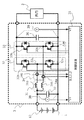
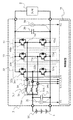
図1は、本発明の実施の形態1に係る電力変換装置の構成例を示す図である。始めに図1を参照し、電力変換装置3の構成について具体的に説明する。
FIG. 1 is a diagram showing a configuration example of a power conversion device according to a first embodiment of the present invention. First, the configuration of the
図1に構成例を示す電力変換装置3は、2つのハーフブリッジ回路を電圧変換用の電圧変換回路32、33として備えたフルブリッジ型のDC(Direct Current)/DCコンバータである。この電力変換装置3には、バッテリ1が電源として接続されると共に、負荷2が接続される。それにより、電力変換装置3は、バッテリ1から供給された電力の電圧を、負荷2にとって望ましい電圧に変換し、電圧を変換させた後の電力を負荷2に供給するようになっている。なお、負荷2の種類は、特に限定されない。その負荷2には、インバータ等の他の電力変換装置が含まれていても良い。
The
バッテリ1の正極端子は、コンタクタ10の一端と接続されている。バッテリ1の負極端子は、平滑コンデンサ37の一端と接続されている。平滑コンデンサ37の他端は、コンタクタ10の他端と接続されている。平滑コンデンサ37の両端には、その両端間の電圧値V1を検出するための電圧センサ38が接続されている。電圧値V1を示す信号は、電圧センサ38から制御装置35に出力される。なお、コンタクタ10は、例えばバッテリ1に備えられるか、或いはバッテリ1及び電力変換装置3とは別に設けられるものである。ここでは便宜的に、コンタクタ10は、一つの部品として設けられたものと想定する。電力変換装置3が電動車両に搭載されている場合、コンタクタ10の開閉制御は、例えばECU(Electronic Control Unit)により行われる。
The positive electrode terminal of the
平滑コンデンサ37の他端には、リアクトル群31を構成するリアクトル31a、31bの各一端が接続されている。リアクトル31aの他端は、電圧変換回路32を構成する2つのスイッチング素子32a、32b間の接続点32cと接続されている。リアクトル31bの他端は、電圧変換回路33を構成する2つのスイッチング素子33a、33b間の接続点33cと接続されている。
One ends of the
2つの電圧変換回路32、33に用いられたスイッチング素子32a〜33bは、IGBT(Insulated Gate Bipolar Transistor)のコレクタ・エミッタ間にダイオードを逆向きに並列接続させたデバイスである。それにより、ダイオードのアノード及びカソードは、エミッタ及びコレクタにそれぞれ接続されている。スイッチング素子32a〜33bは、IGBTを用いたデバイスに限定されない。スイッチング素子32a〜33bは、MOSFET(Metal-Oxide-Semiconductor Field-Effect Transistor)であっても良く、SiC(Silicon Carbide)、GaN(Gallium Nitride)などを用いたワイドバンドギャップ半導体により形成されたものであっても良い。
The
電圧変換回路32、33にそれぞれ接続させたリアクトル31a、31bは、バッテリ1から供給される電力の電圧を昇圧させる機能を備える。また、負荷2の両端間に接続される平滑コンデンサ36に蓄えられた電荷を放電させる際に流れる放電電流を抑制させる機能も備える。
The
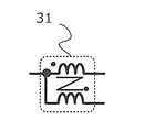
リアクトル群31は、図9に示すように、リアクトル31a、31bを逆極性に接続させた磁気結合型のもの、例えばトランスであっても良い。磁気結合型のリアクトル群31を採用した場合、リアクトル群31を小型化できることから、電力変換装置3もより小型化させることができる。
As shown in FIG. 9, the
電流センサ群34は、リアクトル群31を構成する各リアクトル31a、31bの電流値IL2、IL1を検出するための複数の電流センサである。そのために、電流センサ群34は、リアクトル31aに流れる電流の値IL2を検出するための電流センサ34b、及びリアクトル31bに流れる電流の値IL1を検出するための電流センサ34aを含む。電流値IL2を示す信号は、電流センサ34bから制御装置35に出力される。電流値IL1を示す信号は、電流センサ34aから制御装置35に出力される。リアクトル31aを流れる電流は、電圧変換回路32を流れる電流に相当する。リアクトル31bを流れる電流は、電圧変換回路33を流れる電流に相当する。
The
電圧変換回路32は、2つのスイッチング素子32a、32bを直列に接続させた構成である。スイッチング素子32bを構成するIGBTのコレクタは、負荷2の一端、及び平滑コンデンサ36の一端に接続されている。スイッチング素子32aを構成するIGBTのエミッタは、負荷2の他端、及び平滑コンデンサ36の他端に接続されている。それにより、接続点32cは、スイッチング素子32bを構成するIGBTのエミッタと、スイッチング素子32aを構成するIGBTのコレクタとに接続されている。
The
電圧変換回路33は、2つのスイッチング素子33a、33bを直列に接続させた構成である。スイッチング素子33bを構成するIGBTのコレクタは、負荷2の一端、及び平滑コンデンサ36の一端に接続されている。スイッチング素子33aを構成するIGBTのエミッタは、負荷2の他端、及び平滑コンデンサ36の他端に接続されている。それにより、接続点33cは、スイッチング素子33bを構成するIGBTのエミッタと、スイッチング素子33aを構成するIGBTのコレクタとに接続されている。
The
平滑コンデンサ36の両端間には、その両端間の電圧値V2を検出するための電圧センサ39が接続されている。電圧値V2を示す信号は、電圧センサ39から制御装置35に出力される。
A
制御装置35は、2つの電圧センサ38、39がそれぞれ検出した電圧値V1、V2のうちの一方、及び2つの電流センサ34a、34bがそれぞれ検出した電流値IL2、IL1を処理し、4つのスイッチング素子32a〜33bのオンオフ駆動を行う。この制御装置35は、本実施の形態における制御部、及び電力変換制御装置に共に相当する。ここでは、電力変換装置3の制御装置35を除く部分は「電力変換回路」と表記して区別する。
The
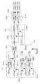
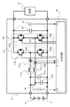
次に図2を参照し、この制御装置35、つまり本実施の形態における電力変換制御装置の構成について具体的に説明する。図2は、本発明の実施の形態1に係る電力変換制御装置の構成例を示す図である。
Next, with reference to FIG. 2, the configuration of the
図2に示すように、制御装置35は、電流エラー量生成部351、電流制御器352、デューティ生成部353、ゲート信号生成部354、第1の電圧制御部355a、第2の電圧制御部355b、及び切替器356を備える。本実施の形態では、例えばゲート信号生成部354を除く構成要素は、一つの情報処理装置、例えばマイクロコンピュータにより実現されていてもよい。その場合、マイクロコンピュータは、ゲート信号生成部354を除く構成要素を実現させるための処理を実行することにより、制御装置35の一部となっている。このことから、本実施の形態における電力変換制御装置は、広義には、図2に示す全ての構成要素を含む。狭義には、本実施の形態における電力変換制御装置には、ゲート信号生成部354は含まれない。
As shown in FIG. 2, the
先ず、制御装置35の動作の概略について説明する。制御装置35は、PWM(Pulse Width Modulation)制御により、各スイッチング素子32a〜33bをオンオフ駆動する。平滑コンデンサ36の電荷の放電を想定しない通常時、制御装置35は、電圧値V2が、設定された基準電圧値V2refと一致するように、スイッチング素子32a〜33bをオンオフ駆動するうえでのデューティ比Dutyを決定する。制御装置35は、電流値IL1、IL2間の差が0となるように、このデューティ比Dutyを操作する。その操作により、デューティ比Dutyから、電圧変換回路32用のデューティ比Duty32、電圧変換回路33用のデューティ比Duty33が生成される。ゲート信号生成部354は、生成されたデューティ比Duty32、Duty33に従って、電圧変換回路32の2つのスイッチング素子32a、32b、及び電圧変換回路33の2つのスイッチング素子33a、33bをオンオフ駆動するための信号を生成して出力する。
First, the outline of the operation of the
ゲート信号生成部354が生成する信号は、スイッチング素子32a〜33bを構成する各IGBTのゲートに入力される信号である。図2に表記の「Gate_32a」は、スイッチング素子32aを構成するIGBTのゲートに入力される信号を表している。同様に、「Gate_32b」「Gate_33a」「Gate_33b」は、それぞれ、スイッチング素子32b〜33bを構成する各IGBTのゲートに入力される信号を表している。
The signal generated by the gate
デューティ比Dutyの操作量は、電流値IL1、IL2を用いて決定される。本実施の形態では、このことに着目し、平滑コンデンサ36の電荷の放電を想定する放電時、その操作量を、放電を想定したものに切り替えるようにしている。それにより、平滑コンデンサ36の電荷のより短時間での放電を実現させる。平滑コンデンサ36の電荷をより短時間で放電させることにより、より高い安全性が確保される。
The amount of operation of the duty ratio Duty is determined by using the current values IL1 and IL2. In the present embodiment, paying attention to this, at the time of discharging assuming discharge of the electric charge of the smoothing
電流エラー量生成部351は、通常時、電流値IL1、IL2間の差分ILerr1を電流エラー量ILerrとして生成し出力する。また、電流エラー量生成部351は、平滑コンデンサ36の電荷を放電させる場合、その差分ILerr1に対し、設定された値を加算し、その加算結果を電流エラー量ILerrとして出力する。そのために、電流エラー量生成部351は、設定値切替器351a、減算器351b、及び加算器351cを備えている。
The current error
減算器351bは、電流値IL1から電流値IL2を減算することにより差分ILerr1を算出する。加算器351cは、差分ILerr1に、設定値切替器351aが出力する値ILerr2を加算することにより、電流エラー量ILerrを算出する。この電流エラー量ILerrが、電流エラー量生成部351から電流制御器352に出力される。
The subtractor 351b calculates the difference ILERr1 by subtracting the current value IL2 from the current value IL1. The adder 351c calculates the current error amount ILERr by adding the value ILERr2 output by the
電流値IL1、IL2は共に変動する。そのため、減算器351bでの減算に用いられる実際の電流値IL1、IL2は、例えば定めた時間での平均値か、或いはフィルタ処理した値である。 The current values IL1 and IL2 both fluctuate. Therefore, the actual current values IL1 and IL2 used for the subtraction by the subtractor 351b are, for example, the average value at a predetermined time or the filtered value.
設定値切替器351aは、コマンドとして機能する2値の信号、つまりH(High)、及びL(Low)の2つの状態を有する信号である指示1により、出力する値ILerr2の内容を切り替える。H、言い換えれば論理値が1の指示1は、平滑コンデンサ36の電荷の放電動作を要求する。L、言い換えれば論理値が0の指示1は、通常時の動作、つまり負荷2への電力供給動作を要求する。
The
負荷2にモータが含まれている場合、指示1は、平滑コンデンサ36の電荷を放電すべき状況時の他に、発電機として機能しているモータからの電力である回生電力が供給される状況時にもHになる。この2つの状況時の放電電流、及び回生電力は共に、バッテリ1の充電、及びバッテリ1に接続された別の負荷への電力供給に用いることができる。第2の電圧制御部355bは、バッテリ1の充電、及び別の負荷への電力供給を想定したものである。
When the
なお、回生電力を電力供給に用いる場合であっても、回生電力は電力変換回路内で消費される。それにより、電力変換回路は、電力変換装置3が電動車両等に搭載されている場合、回生ブレーキとしても機能する。このため、電動車両に搭載する機械ブレーキに求められる制動力はより小さいものとなる。
Even when the regenerative power is used for power supply, the regenerative power is consumed in the power conversion circuit. As a result, the power conversion circuit also functions as a regenerative brake when the
コンタクタ10は、バッテリ1と電力変換装置3との間の電気的な接続、及びその接続の切断を可能にする。バッテリ1から電力を供給する状況では、コンタクタ10は閉状態とされ、バッテリ1と電力変換装置3との間は接続される。放電電流が流れる状況、及び回生電力が供給される状況では、コンタクタ10は、バッテリ1と電力変換装置3との間の接続を切断する開状態、及び閉状態のうちの何れかとなる。これは、例えばバッテリ1が充電可能な状態であれば、上記のように、放電電流、及び回生電力は共にバッテリ1の充電に利用できるからである。以下、混乱を避けるために、負荷2への電力供給を行う状況は「通常状況」と表記し、それ以外の状況は「放電実行状況」と総称する。放電実行状況には、平滑コンデンサ36の電荷による放電電流、或いは回生電力を単に消費する状況、及び、その放電電流、或いは回生電力を用いてバッテリ1、或いは別の負荷に電力供給する状況が含まれる。
The
設定値切替器351aは、指示1がLであった場合、0の値ILerr2を出力する。それにより、電流エラー量生成部351は、差分ILerr1を電流エラー量ILerrとして出力する。この結果、電流エラー量生成部351は、電流値IL1、IL2を一致させるように機能する。
When the
一方、指示1がHであった場合、設定値切替器351aは、例えば定められた設定値ILsetを値ILerr2として出力する。そのため、電流エラー量生成部351は、差分ILerr1に設定値ILsetを加算して得られる加算結果を電流エラー量ILerrとして出力する。この結果、電流エラー量生成部351は、平滑コンデンサ36の電荷の放電を効率的に行えるように機能する。
On the other hand, when the
電流制御器352は、電流エラー量生成部351から入力した電流エラー量ILerrを用いて、デューティ比Dutyの操作量ΔDを算出してデューティ生成部353に出力する。操作量ΔDの算出には、周知の技術、例えばP制御、PI制御、或いはPID(Proportional-Integral-Differential)制御を用いることができる。
The
第1の電圧制御部355aは、電圧値V2が基準となる目標電圧値V2refと一致させるためのデューティ比Duty2を生成する。そのために、第1の電圧制御部355aは、減算器3551、及び電圧制御器3552を備えている。
The first
減算器3551は、目標電圧値V2refから電圧値V2を減算することにより、それらの間の差分V2errを算出する。電圧制御器3552は、差分V2errを用いて、電圧値V2を目標電圧値V2errと一致させるためのデューティ比Duty2を算出する。算出されたデューティ比Duty2は、切替器356に出力される。差分V2errを用いたデューティ比Duty2の算出には、周知の技術、例えばP制御、PI制御、或いはPID制御を用いることができる。
The
第2の電圧制御部355bは、第1の電圧制御部355aとは異なり、電圧値V1が基準となる目標電圧値V1refと一致させるためのデューティ比Duty1を生成し、生成したデューティ比Duty1を切替器356に出力する。そのために、第2の電圧制御部355bは、第1の電圧制御部355aと同様に、減算器3551、及び電圧制御器3552を備えている。それら構成要素の動作は第1の電圧制御部355aと同様なため、詳細な説明は省略する。
Unlike the first
切替器356は、例えば指示1と同様な2値の信号である指示2により、入力したデューティ比Duty1、Duty2のうちの一方を選択し、選択した方をデューティ比Dutyとしてデューティ生成部353に出力する。例えば切替器356は、指示2がLであった場合、デューティ比Duty2を選択し、選択したデューティ比Duty2をデューティ比Dutyとして出力する。指示2がHであった場合、切替器356は、デューティ比Duty1を選択し、選択したデューティ比Duty1をデューティ比Dutyとして出力する。
The
指示2がHとなるのは、放電実行状況時であり、且つ電圧値V1を維持すべき時である。(例えば、バッテリ1側にシステムに重要な機器が接続されてコンタクタ10は、放電実行状況時となる前に開状態とされる。バッテリ1に別の負荷としてシステムに重要な機器が接続されているような場合、電圧値V1は維持させる必要がある。指示1は、切替器356がデューティ比Duty1をデューティ比Dutyとして出力した後、Hとさせる必要がある。このことから、指示1は、指示2がHとなった後にHとなる。
The
なお、本実施の形態では、放電実行状況時に、バッテリ1と接続された別の負荷に電力を供給することも想定している。しかし、その想定は行わなくとも良い。それにより、第2の電圧制御部355bは設けなくとも良い。第2の電圧制御部355bを設けない場合、デューティ比Duty1の代わりに、所定のデューティ比、例えば50%固定のデューティ比を想定し、設定値切替器351aに値ILerr2として出力させる設定値ILsetを設定すれば良い。
In this embodiment, it is also assumed that power is supplied to another load connected to the
デューティ生成部353は、スイッチング素子32a〜33bのオンオフ駆動に用いるデューティ比Duty32、Duty33を生成する。デューティ比Duty32、Duty33の生成は、電流制御器352から入力した操作量ΔDを用いて、切替器356から入力したデューティ比Dutyを操作することで行われる。そのために、デューティ生成部353は、減算器353a、及び加算器353bを備えている。
The
減算器353aは、デューティ比Dutyから操作量ΔDを減算する。その減算結果がデューティ比Duty32としてゲート信号生成部354に出力される。
The
一方、加算器353bは、デューティ比Dutyに操作量ΔDを加算する。その加算結果がデューティ比Duty33としてゲート信号生成部354に出力される。
On the other hand, the
ゲート信号生成部354は、2つの信号生成器354a、354bを備える。デューティ比Duty32は、信号生成器354aに入力され、デューティ比Duty33は、信号生成器354bに入力される。
The
信号生成器354aは、デューティ比Duty32に従って、電圧変換回路32を構成する2つのスイッチング素子32a,32bをオンオフ駆動するための信号Gate_32a、Gate_32bを生成する。信号Gate_32a、Gate_32bは、互いに相補的な信号であり、一方がHのときに他方はLとなる。デューティ比Duty32は、スイッチング素子32bを構成するIGBTが1周期のうちでオン駆動される時間の割合を示す値である。この周期は、PWM制御を行ううえでの単位時間である周期、つまりスイッチング周期である。
The
信号生成器354bは、デューティ比Duty33に従って、電圧変換回路33を構成する2つのスイッチング素子33a,33bをオンオフ駆動するための信号Gate_33a、Gate_33bを生成する。信号Gate_33a、Gate_33bも、互いに相補的な信号であり、一方の信号がHのときに他方の信号はLとなる。電圧変換回路は電圧変換回路32、33の2つであることから、信号Gate_33a、Gate_33bは、信号Gate_32a、Gate_32bとは位相が逆、つまり180度ズレている。
The
上記の構成において、第1の電圧制御部355aは、本実施の形態における第1の条件設定部に相当する。生成されるデューティ比Duty2は、第1の駆動条件に相当する。第2の電圧制御部355bは、本実施の形態における第3の条件設定部に相当する。生成されるデューティ比Duty1は、第3の駆動条件に相当する。デューティ生成部353は、本実施の形態における第2の条件設定部に相当する。デューティ比Duty32、Duty33は共に、第2の駆動条件に相当する。切替器356は、本実施の形態における選択部に相当する。
In the above configuration, the first
電流エラー量生成部351の減算器351b、及び電流制御器352は、本実施の形態における変更量決定部に相当する。操作量ΔDは、本実施の形態における変更量に相当する。設定値切替器351a、及び加算器351cは、本実施の形態における狭義の変更量操作部に相当する。広義の変更量操作部には、電流制御器352が更に含まれる。これは、設定値切替器351aが値ILerr2として設定値ILsetを出力したことによる最終的な結果は、電流制御器352の処理により得られるからである。ゲート信号生成部354は、本実施の形態における信号生成部に相当する。
The subtractor 351b of the current error
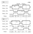
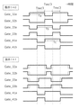
図3は、通常状況時、及び放電実行状況時にそれぞれ生成される各信号例を説明する図である。図3において、上段は、通常状況時に生成される各信号例を示し、下段は、放電実行状況時に生成される各信号例を示している。通常状況時とは、指示1が0、つまりLとなっている状況時であり、放電実行状況時とは、指示1が1、つまりHとなっている状況時である。図3において、各信号、つまり信号Gate_32a、Gate_32b、Gate_33a、Gate_33bは、H、Lの2値で信号レベルを表している。
FIG. 3 is a diagram illustrating an example of each signal generated in a normal situation and a discharge execution situation, respectively. In FIG. 3, the upper row shows an example of each signal generated in a normal situation, and the lower row shows an example of each signal generated in a discharge execution situation. The normal situation is a situation where the
図3において、「Tsw」は、スイッチング周期を表している。「Ta」は、通常状況時における信号Gate_32aのHが継続する時間であるH時間、言い換えれば信号Gate_32bのLが継続する時間であるL時間を表している。「Ta’」は、放電実行状況時における信号Gate_32aのH時間を表している。それにより、通常状況時では、デューティ比Duty32=Ta/Tswである。 In FIG. 3, "Tsw" represents a switching period. “Ta” represents the H time, which is the time during which H of the signal Gate_32a continues in a normal situation, in other words, the L time, which is the time during which L of the signal Gate_32b continues. "Ta'" represents the H time of the signal Gate_32a in the discharge execution state. As a result, in a normal situation, the duty ratio Duty32 = Ta / Tsw.
また、「Tb」は、通常状況時における信号Gate_33aのH時間、言い換えれば信号Gate_33bのL時間を表している。「Tb’」は、放電実行状況時における信号Gate_33aのH時間を表している。 Further, "Tb" represents the H time of the signal Gate_33a in a normal situation, in other words, the L time of the signal Gate_33b. "Tb'" represents the H time of the signal Gate_33a in the discharge execution state.
H時間Ta、Ta’の差(=Ta−Ta’)は、デューティ比Dutyが同じであり、且つ電流値IL1、IL2の和(=IL1+IL2)も同じと仮定した場合、操作量ΔDを用いた減算操作により生じる。その仮定では、通常状況時、電流制御器352が操作量ΔDの生成に用いる電流エラー量ILerrと、放電実行状況時、電流制御器352が操作量ΔDの生成に用いる電流エラー量ILerrとの間には、上記のように、設定値ILsetの差がある。このことから、図3は、設定値ILsetにより、操作量ΔDの内容を間接的に制御できることを表している。
As for the difference between H time Ta and Ta'(= Ta-Ta'), the manipulated variable ΔD was used assuming that the duty ratio duty is the same and the sum of the current values IL1 and IL2 (= IL1 + IL2) is also the same. It is caused by the subtraction operation. Under that assumption, between the current error amount ILERr used by the
なお、設定値ILsetに応じたデューティ比Dutyの操作は、操作量ΔDによる操作とは別に行っても良い。つまり、設定値ILsetに応じたデューティ比Dutyの操作は、直接的に行うようにしても良い。 The duty ratio duty operation according to the set value ILset may be performed separately from the operation using the operation amount ΔD. That is, the duty ratio duty operation according to the set value ILset may be performed directly.
図3の上段、及び下段には、モードとして、1、3、4の数値を表記している。このモードは、電力変換回路内で形成される閉回路に対応したものであり、数値は、実際に形成される閉回路の種類を表している。ここで、図4〜図7を参照し、各ノードで形成される閉回路について具体的に説明する。図4〜図7は、それぞれモード1〜4で形成される閉回路の例を説明する図である。
モード1では、図4に示すように、平滑コンデンサ36を含む閉回路、つまり平滑コンデンサ36→スイッチング素子32b→リアクトル31a→リアクトル31b→スイッチング素子33a→平滑コンデンサ36、の経路で平滑コンデンサ36から放電電流が流れる閉回路が形成される。この閉回路により、モード1では、平滑コンデンサ36に蓄えられた電荷を直接、放電させるとともにリアクトル32a、32bにエネルギーを移すことができる。
In
モード4では、図7に示すように、平滑コンデンサ36を含む閉回路、つまり平滑コンデンサ36→スイッチング素子33b→リアクトル31b→リアクトル31a→スイッチング素子32a→平滑コンデンサ36、の経路で平滑コンデンサ36から放電電流が流れる閉回路が形成される。この閉回路により、モード4でも、平滑コンデンサ36に蓄えられた電荷を直接、放電させるとともにリアクトル31a、31bにエネルギーを移すことができる。
In
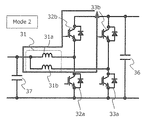
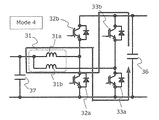
モード2では、図5に示すように、平滑コンデンサ36を含む閉回路は形成されず、リアクトル群31を含む閉回路が形成される。その閉回路では、リアクトル群31に蓄えられたエネルギーにより、例えばリアクトル31a→リアクトル31b→スイッチング素子33b→スイッチング素子32b→リアクトル31a、の経路で電流が流れる。平滑コンデンサ36から放電電流が流れる場合、リアクトル群31にエネルギーが蓄えられる。そのため、この閉回路に電流が流れることにより、平滑コンデンサ36からの放電電流が流れる閉回路が形成されていなくとも、導通損失、つまり電力変換回路内での電力損失が発生し、平滑コンデンサ36を含む電力変換回路の電荷の放電が実現される。
In
モード3でも、図6に示すように、平滑コンデンサ36を含む閉回路は形成されず、リアクトル群31を含む閉回路が形成される。その閉回路では、リアクトル群31に蓄えられたエネルギーにより、例えばリアクトル31a→リアクトル31b→スイッチング素子33a→スイッチング素子32a→リアクトル31a、の経路で電流が流れる。この閉回路に電流が流れることにより、モード3でも、平滑コンデンサ36を含む電力変換回路の電荷の放電が実現される。
Even in
モード1及びモード4で形成される閉回路は共に、本実施の形態における第1の閉回路に相当する。モード2で形成される閉回路は、本実施の形態における第2の閉回路に相当する。
Both the closed circuit formed in the
図3の下段では、モードは、モード1→モード3→モード4→モード3、の順序でサイクリックに遷移する。その遷移は、昇圧比によって変化する。昇圧比によっては、モードは、モード1→モード2→モード4→モード2、の順序でサイクリックに遷移する。
In the lower part of FIG. 3, the modes transition cyclically in the order of
上記のような遷移では、常に閉回路が形成される。しかし、スイッチング周期内に、閉回路が形成されない期間を設けても良い。このこともあり、モード遷移、つまり形成させる閉回路の種類、及びその順序、等は特に限定されない。 In the transition as described above, a closed circuit is always formed. However, a period during which the closed circuit is not formed may be provided within the switching cycle. For this reason, the mode transition, that is, the type of closed circuit to be formed, the order thereof, and the like are not particularly limited.
図3の下段に示すようなモード遷移により、平滑コンデンサ36を含む閉回路の他に、その平滑コンデンサ36を含まない閉回路が形成される。そのため、平滑コンデンサ36を含む閉回路が形成されていない間でも、電力変換回路内の電力が消費される。この電力消費により、平滑コンデンサ36の電荷の放電はより効率的に行えるようになる。この結果、平滑コンデンサ36の電荷の放電もより短時間に行うことができる。
By the mode transition as shown in the lower part of FIG. 3, in addition to the closed circuit including the smoothing
電荷は、平滑コンデンサ36の他に、平滑コンデンサ37にも蓄えられる。平滑コンデンサ37に蓄えられた電荷は、モード1及びモード4で形成される閉回路により放電させることができる。本実施の形態では、平滑コンデンサ37を含む閉回路は、モード3でも形成される。そのため、平滑コンデンサ37の電荷の放電もより短時間に行うことができる。
The electric charge is stored in the smoothing
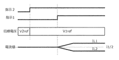
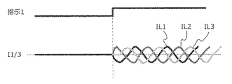
図8は、リアクトル群を構成する各リアクトルの放電実行状況時における電流値の変化の例を説明する図である。図8では、各リアクトル31a、31bの電流値IL1、IL2に加え、指示1、指示2、及び指示2によって切り換えられる目標電圧値V1ref、V2refを示している。ここでの電流値IL1、IL2は、上記のように、平均値か、或いはフィルタ処理した値である。
FIG. 8 is a diagram illustrating an example of a change in the current value of each of the reactors constituting the reactor group when the discharge is executed. FIG. 8 shows the target voltage values V1ref and V2ref switched by the
図8中の「I1」は、バッテリ1から供給される電力の電流値を表している。電力変換装置3は2つの電圧変換回路32、33を備えていることから、電流値IL1とIL2の和はI1であり、通常、電流値IL1、IL2は、I1/2となっている。
“I1” in FIG. 8 represents the current value of the electric power supplied from the
上記のように、通常状況時には、指示1、及び指示2は共にLである。通常状況からコンタクタ10が開状態となり、バッテリ1との接続が切断され放電実行状況に変化する場合、図8に示すように、指示1は、指示2がHとなった後にHとなる。指示1がHとなることにより、平滑コンデンサ36の電荷の放電を想定したスイッチング素子32a〜33bのオンオフ駆動が開始される。言い換えれば、図4〜図7に示すような閉回路の形成による平滑コンデンサ36の電荷の直接的な放電、及びその放電によってリアクトル群31に生じるエネルギーの消費が開始される。その結果、図8に示すように、リアクトル31a、31bの電流値IL2、IL1の間には、電流エラー量生成部315で設定される設定値ILsetの差が発生することとなる。
As described above, in a normal situation, both
電力変換回路に用いられる部品には、通常、上限温度が定められている。このことから、スイッチング素子32a〜33bのうちの少なくとも一つ、平滑コンデンサ36、37のうちの少なくとも一つ、及びリアクトル31a、31bのうちの少なくとも一つのうちの何れかに温度検出用の温度センサを設け、検出された温度を制御に用いても良い。例えば検出された温度が定めた上限値を超えた場合、指示1をHからLに変更しても良い。そのようにしても、単位時間当たりの電流量は、温度が上限値を超える前より低下することから、上限値を超える温度が検出された部品はもとより、他の電流によって温度が上昇する部品の温度もより低くさせることができる。従って、電力変換回路を構成する部品をより保護することができる。
The upper limit temperature is usually set for the parts used in the power conversion circuit. From this, a temperature sensor for temperature detection is used in at least one of the
温度の抑制は、リアクトル31a、31bでは高周波化が望ましく、スイッチング素子32a〜33bでは低周波化が望ましい。このことから、リアクトル31a、31bのうちの一方、及びスイッチング素子32a〜33bのうちの何れかの温度を検出するために複数の温度センサを設けても良い。そのように複数の温度センサを設けた場合、検出された温度が上限値を超えた部品の種類に応じて、スイッチング周期、つまりスイッチング周波数を変更するようにしても良い。
For temperature suppression, it is desirable to increase the frequency of the
電流センサ群34を構成する何れかの電流センサに異常が発生する可能性がある。何れかの電流センサに異常が発生した場合、電流値IL1、IL2を用いた適切なフィードバック制御は不可能となる。このことから、何れかの電流センサに異常が発生した場合、操作量ΔDを予め定めた固定値とし、電流値IL1、IL2をフィードバック制御に反映させないようにしても良い。この固定値は、例えば2つ以上、用意することにより、指示1がLか否かに応じて固定値を切り換えれば良い。そのように固定値を切り換えるようにした場合、通常状況時、放電実行状況時ともに、電力変換装置3を動作させることができる。放電実行状況時には、平滑コンデンサ36の電荷の放電に要する時間の短縮化も実現させることができる。
An abnormality may occur in any of the current sensors constituting the
異常は、スイッチング素子32a〜33bのうちの何れかに発生する可能性がある。アームであるスイッチング素子32b、33bのうちの何れかにオン駆動できないオフ故障が発生した場合、そのオフ故障が発生したスイッチング素子のオンオフ駆動を停止し、故障したスイッチング素子を除く残りのスイッチング素子のオンオフ駆動を行うようにしても良い。そのようなオンオフ駆動を行う場合、オフ故障が発生したスイッチング素子は、ダイオードとしてのみ使用することになる。
The abnormality may occur in any of the
オフ故障が発生したスイッチング素子のダイオードとしてのみの使用は、例えば2つの信号生成器354a、354bのそれぞれに、オフ故障が発生したスイッチング素子に応じて生成する信号の内容を変更させることにより実現できる。そのように、オフ故障が発生したアームに応じて、生成する信号の内容を変更することにより、オフ故障の発生後も電力変換装置3を動作させることができる。制御が複雑になるのを抑制するために、電流値IL1、IL2を用いたフィードバック制御は停止させるのが望ましい。
The use of the switching element in which the off failure has occurred only as a diode can be realized, for example, by causing each of the two
実施の形態2.
図10は、本発明の実施の形態2に係る電力変換装置の構成例を示す図である。本実施の形態では、平滑コンデンサ37の代わりに、2つの平滑コンデンサ37B、37Cを用いている。図10に示すように、平滑コンデンサ37Bは、リアクトル31aのバッテリ1側の一端と、バッテリ1の負極端子との間に接続されている。平滑コンデンサ37Cは、リアクトル31bのバッテリ1側の一端と、バッテリ1の負極端子との間に接続されている。
FIG. 10 is a diagram showing a configuration example of the power conversion device according to the second embodiment of the present invention. In this embodiment, two smoothing capacitors 37B and 37C are used instead of the smoothing
電力変換回路が図10に示すような構成であっても、制御装置35として、基本的に上記実施の形態1の制御装置35を用いることができる。その制御装置35を用いることにより、本実施の形態でも、上記実施の形態1と同様の効果を得ることができる。
Even if the power conversion circuit has a configuration as shown in FIG. 10, basically, the
実施の形態3.
上記実施の形態1、2では、電力変換回路が備える電圧変換回路は2つとなっている。これに対し、本実施の形態3では、電圧変換回路は3つとなっている。
In the first and second embodiments, the power conversion circuit includes two voltage conversion circuits. On the other hand, in the third embodiment, there are three voltage conversion circuits.
図11は、本発明の実施の形態3に係る電力変換装置の構成例を示す図である。本実施の形態では、図11に示すように、スイッチング素子41a、41bが直列に接続された構成の電圧変換回路41が平滑コンデンサ36の両端間に更に接続されている。バッテリ1の正極端子と、2つのスイッチング素子41a、41b間の接続点41cとの間には、リアクトル31cが接続されている。そのリアクトル31cに流れる電流の電流値IL3を検出するために、電流センサ34cが追加されている。
FIG. 11 is a diagram showing a configuration example of the power conversion device according to the third embodiment of the present invention. In the present embodiment, as shown in FIG. 11, a
図12は、本発明の実施の形態3に係る電力変換制御装置の構成例を示す図である。図12では、上記実施の形態1から異なる部分を抽出して構成例を示している。つまり、本実施の形態では、制御装置35は、図12に示す構成要素の他に、第1の電圧制御部355a、第2の電圧制御部355b、及び切替器356を備える。
FIG. 12 is a diagram showing a configuration example of the power conversion control device according to the third embodiment of the present invention. In FIG. 12, a configuration example is shown by extracting a different portion from the first embodiment. That is, in the present embodiment, the
本実施の形態では、電流エラー量生成部351は、図12に示すように、第1の指令値生成部501、第2の指令値生成部502、及び第3の指令値生成部503を備える。
In the present embodiment, as shown in FIG. 12, the current error
第1の指令値生成部501は、演算器511、及び3つの減算器512a〜512cを備えている。演算器511は、電流値IL1〜IL3を入力して、その平均値ILrefXを算出する。この平均値ILrefXは、ILrefX=(IL1+IL2+IL3)/3、により求めることができる。平均値ILrefXは、各減算器512a〜512cに出力される。
The first command
減算器512aは、平均値ILrefXから電流値IL1を減算し、その減算結果ILerrX1を第3の指令値生成部503に出力する。減算器512bは、平均値ILrefXから電流値IL2を減算し、その減算結果ILerrX2を第3の指令値生成部503に出力する。減算器512cは、平均値ILrefXから電流値IL3を減算し、その減算結果ILerrX3を第3の指令値生成部503に出力する。
The
第2の指令値生成部502は、偏流波生成器521を備える。この偏流波生成器521は、電圧変換回路が3つ存在するために、設定値切替器351aの代わりに搭載されたものである。偏流波生成器521は、第3の指令値生成部503に、減算結果ILerrX1〜ILerrX3に対する操作量となる値ILerrY1〜ILerrY3を生成して出力する。
The second command
これらの値ILerrY1〜ILerrY3は、放電実行状況時、つまり指示1がHとなっている状況時か否かに応じて生成方法が異なる。指示1がLの状況時では、例えば値ILerrY1〜ILerrY3は全て0である。指示1がHの状況時では、例えば値ILerrY1〜ILerrY3は、以下のようにして生成される。
ILerrY1=Asinωt
ILerrY2=Asin(ωt+2π/3)
ILerrY3=Asin(ωt−2π/3)
ここで、Aは定数、ωはスイッチング周波数に対応する角速度、tは指示1がHとなってから経過した時間、である。
The generation method of these values ILErrY1 to ILErrY3 differs depending on whether or not the discharge execution state, that is, the situation where the
ILErrY1 = Asinωt
ILRY2 = Asin (ωt + 2π / 3)
ILErrY3 = Asin (ωt-2π / 3)
Here, A is a constant, ω is an angular velocity corresponding to the switching frequency, and t is the time elapsed since the
偏流波生成器521は、指示1がHの場合に、値ILerrY1〜ILerrY3を偏流波値として生成する。値ILerrY1〜ILerrY3は、上記実施の形態1における設定値ILsetのように機能する。値ILerrY1〜ILerrY3の合計値は0となる。
The
第3の指令値生成部503は、3つの加算器531a〜531cを備えている。加算器531aは、減算結果ILerrX1に値ILerrY1を加算し、その加算結果を差分ILerr11として電流制御器352aに出力する。同様に、加算器531bは、減算結果ILerrX2に値ILerrY2を加算し、その加算結果を差分ILerr12として電流制御器352bに出力する。加算器531cは、減算結果ILerrX3に値ILerrY3を加算し、その加算結果を差分ILerr13として電流制御器352cに出力する。
The third command
差分ILerr11、ILerr12、ILerr13は共に、上記実施の形態1における差分ILerr1に相当する情報である。電流制御器352aは、上記実施の形態1と同様に、差分ILerr11を用いて、操作量ΔDaを生成し、デューティ生成部353に出力する。電流制御器352bも、上記実施の形態1と同様に、差分ILerr12を用いて、操作量ΔDbを生成し、デューティ生成部353に出力する。電流制御器352cも、上記実施の形態1と同様に、差分ILerr13を用いて、操作量ΔDcを生成し、デューティ生成部353に出力する。
The difference ILERr11, ILERr12, and ILERr13 are all information corresponding to the difference ILERr1 in the first embodiment. Similar to the first embodiment, the
デューティ生成部353は、3つの加算器353b〜353dを備える。加算器353cは、切替器356から入力したデューティ比Dutyに、操作量ΔDaを加算し、その加算結果をデューティ比Duty32としてゲート信号生成部354に出力する。加算器353bは、デューティ比Dutyに、操作量ΔDbを加算し、その加算結果をデューティ比Duty33としてゲート信号生成部354に出力する。加算器353dは、デューティ比Dutyに、操作量ΔDcを加算し、その加算結果をデューティ比Duty41としてゲート信号生成部354に出力する。
The
ゲート信号生成部354は、3つの信号生成器354a〜354cを備える。デューティ比Duty32は、信号生成器354aに入力され、デューティ比Duty33は、信号生成器354bに入力され、デューティ比Duty41は、信号生成器354cに入力される。
The
信号生成器354aは、デューティ比Duty32に従って、電圧変換回路32を構成する2つのスイッチング素子32a,32bをオンオフ駆動するための信号Gate_32a、Gate_32bを生成する。信号Gate_32a、Gate_32bは、互いに相補的な信号であり、一方の信号がHのときに他方の信号はLとなる。
The
信号生成器354bは、デューティ比Duty33に従って、電圧変換回路33を構成する2つのスイッチング素子33a,33bをオンオフ駆動するための信号Gate_33a、Gate_33bを生成する。信号Gate_33a、Gate_33bも、互いに相補的な信号である。
The
信号生成器354cは、デューティ比Duty41に従って、電圧変換回路41を構成する2つのスイッチング素子41a,41bをオンオフ駆動するための信号Gate_41a、Gate_41bを生成する。信号Gate_41a、Gate_41bも、互いに相補的な信号である。
The
図13は、本発明の実施の形態3に係る電力変換制御装置によって通常状況時、及び放電実行状況時にそれぞれ生成される各信号例を説明する図である。図13において、上段は、通常状況時に生成される各信号例を示し、下段は、放電実行状況時に生成される各信号例を示している。 FIG. 13 is a diagram illustrating an example of each signal generated by the power conversion control device according to the third embodiment of the present invention in a normal situation and a discharge execution state, respectively. In FIG. 13, the upper row shows each signal example generated in the normal situation, and the lower row shows each signal example generated in the discharge execution situation.
図13中の「Tc」は、通常状況時における信号Gate_41aのH時間、言い換えれば信号Gate_41bのL時間を表している。通常状況時では、デューティ比Duty41=Tc/Tsw、である。 “Tc” in FIG. 13 represents the H time of the signal Gate_41a in a normal situation, in other words, the L time of the signal Gate_41b. Under normal circumstances, the duty ratio Duty41 = Tc / Tsw.
本実施の形態では、3つの電圧変換回路32、33、41gs備えられている。それにより、図13に示すように、信号Gate_32a、Gate_32bと信号Gate_33a、Gate_33bとの間の位相は120度ズレている。同様に、信号Gate_33a、Gate_33bと信号Gate_41a、Gate_41bとの間の位相も120度ズレている。信号Gate_32a、Gate_32bと信号Gate_41a、Gate_41bとの間の位相も120度ズレている。
In this embodiment, three
図13の下段に示す各信号により、放電実行状況時には、平滑コンデンサ36、3つの電圧変換回路32、33、41、及び3つのリアクトル31a〜31cを含む閉回路が順次、形成される。形成される閉回路には、3つの電圧変換回路32、33、41のうちの上アームがオン駆動された2つの電圧変換回路、及び電圧変換回路32、33、41のうち下アームがオン駆動された一つの電圧変換回路によって形成される閉回路が含まれる。図13に示す信号例では、アームがオン駆動されるのは電圧変換回路33、41であり、下アームがオン駆動されるのは残りの電圧変換回路32である。この閉回路は、本実施の形態における第3の閉回路に相当する。
Each signal shown in the lower part of FIG. 13 sequentially forms a closed circuit including a smoothing
このような閉回路全体のインピーダンスは、平滑コンデンサ36、3つの電圧変換回路32、33、41のうちの2つ、及び3つのリアクトル31a〜31cのうちの2つのみを含む閉回路と比較して小さくなる。そのため、3つの電圧変換回路32、33、41を含む閉回路では、2つの電圧変換回路のみを含む閉回路と比較し、単位時間当たりに流れる電流量がより大きくなる。この結果、平滑コンデンサ36に蓄えられた電荷は、より短時間に放電させることができる。
The impedance of such a closed circuit as a whole is compared to a closed circuit containing only two of the smoothing
図14は、本発明の実施の形態3に係る電力変換装置で放電実行状況時に各リアクトルに流れる電流の値の変化の例を説明する図である。指示1がLとなっている通常状況時、
電圧変換回路が3つであってもバッテリ1からの電力は等配分されることから、各リアクトル31a〜31cの電流値IL1〜IL3はI1/3となっている。
FIG. 14 is a diagram illustrating an example of a change in the value of the current flowing through each reactor during a discharge execution state in the power conversion device according to the third embodiment of the present invention. In a normal situation where
Since the power from the
一方、指示1がHとなっている放電実行状況時にも、各電圧変換回路32、33、41を構成する2つのスイッチング素子は、120度ずつ位相がズレた信号によってオンオフ駆動される。この結果、電流値IL1〜IL3の各間は、120度ずつ位相がズレている。また、電流値IL1〜IL3は、角速度ωで変化する。
On the other hand, even in the discharge execution state in which the
なお、本実施の形態では、電圧変換回路を3つとしているが、電圧変換回路は4つ以上であっても良い。電圧変換回路を4つ以上としても、放電実行状況時には、平滑コンデンサ36、及び3つ以上の電圧変換回路を含む閉回路を形成させれば良い。
In the present embodiment, the number of voltage conversion circuits is three, but the number of voltage conversion circuits may be four or more. Even if the number of voltage conversion circuits is four or more, a closed circuit including the smoothing
1 バッテリ(電源)、2 負荷、3 電力変換装置、10 コンタクタ、31 リアクトル群、31a〜31c リアクトル、32、33、41 電圧変換回路、32a、32b、33a、33b、41a、41b スイッチング素子、34 電流センサ群、34a〜34c 電流センサ、35 制御装置(電力変換制御装置)、36 平滑コンデンサ、37、37B、37C 平滑コンデンサ、38 電圧センサ、39 電圧センサ、351 電流エラー量生成部、352、352a〜352c 電流制御器、353 デューティ生成部、354 ゲート信号生成部、354a〜354c 信号生成器、355a 第1の電圧制御部、355b 第2の電圧制御部、356 切替器。 1 Battery (power supply), 2 Load, 3 Power converter, 10 Contactor, 31 Reactor group, 31a to 31c Reactor, 32, 33, 41 Voltage conversion circuit, 32a, 32b, 33a, 33b, 41a, 41b Switching element, 34 Current sensor group, 34a to 34c current sensor, 35 control device (power conversion control device), 36 smoothing capacitor, 37, 37B, 37C smoothing capacitor, 38 voltage sensor, 39 voltage sensor, 351 current error amount generator, 352, 352a ~ 352c Current controller, 353 duty generator, 354 gate signal generator, 354a to 354c signal generator, 355a first voltage control unit, 355b second voltage control unit, 356 switcher.
モード1では、図4に示すように、平滑コンデンサ36を含む閉回路、つまり平滑コンデンサ36→スイッチング素子32b→リアクトル31a→リアクトル31b→スイッチング素子33a→平滑コンデンサ36、の経路で平滑コンデンサ36から放電電流が流れる閉回路が形成される。この閉回路により、モード1では、平滑コンデンサ36に蓄えられた電荷を直接、放電させるとともにリアクトル31a、31bにエネルギーを移すことができる。
In
Claims (11)
前記平滑コンデンサと並列に接続され、直列に接続された2つのスイッチング素子を上アーム、及び下アームとして各々含む複数の電圧変換回路と、
一端が電源と接続され、他端が前記複数の電圧変換回路のうちの一つを構成する前記2つのスイッチング素子の間にそれぞれ接続されたリアクトルを含むリアクトル群と、
前記平滑コンデンサに蓄えられた電荷を放電させる場合に、前記複数の電圧変換回路を構成する各スイッチング素子のオンオフ駆動により、前記平滑コンデンサ、前記リアクトル群を構成する2つ以上のリアクトル、及び前記複数の電圧変換回路を構成する2つ以上の電圧変換回路を含む第1の閉回路、並びに前記リアクトル群を構成する2つ以上のリアクトル、及び前記複数の電圧変換回路を構成する2つ以上の電圧変換回路の各上アームまたは各下アームを含み、前記平滑コンデンサを含まない第2の閉回路を形成させる制御部と、
を備える電力変換装置。 A smoothing capacitor connected in parallel with the load,
A plurality of voltage conversion circuits including two switching elements connected in parallel with the smoothing capacitor and connected in series as an upper arm and a lower arm, respectively.
A reactor group including a reactor having one end connected to a power supply and the other end connected between the two switching elements constituting one of the plurality of voltage conversion circuits.
When the electric charge stored in the smoothing capacitor is discharged, the smoothing capacitor, the two or more reactors constituting the reactor group, and the plurality of reactors are driven by on / off driving of each switching element constituting the plurality of voltage conversion circuits. A first closed circuit including two or more voltage conversion circuits constituting the voltage conversion circuit, two or more reactors constituting the reactor group, and two or more voltages constituting the plurality of voltage conversion circuits. A control unit that includes each upper arm or each lower arm of the conversion circuit and forms a second closed circuit that does not include the smoothing capacitor.
A power converter equipped with.
請求項1に記載の電力変換装置。 The reactors are magnetically coupled,
The power conversion device according to claim 1.
前記リアクトル群を構成する各リアクトルの電流値を検出する複数の電流センサと、を更に備え、
前記制御部は、
前記電圧センサにより検出された前記電圧値を用いて、前記複数の電圧変換回路を構成する前記各スイッチング素子をオンオフ駆動する第1の駆動条件を決定する第1の条件設定部と、
前記複数の電流センサによりそれぞれ検出された前記電流値を用いて、前記第1の駆動条件に対する変更量を決定する変更量決定部と、
前記変更量を用いて、前記第1の駆動条件を変更した後の駆動条件である第2の駆動条件を設定する第2の条件設定部と、
前記第2の条件設定部が設定した前記第2の駆動条件に従って、前記複数の電圧変換回路を構成する前記スイッチング素子をオンオフ駆動するための信号を生成する信号生成部と、
を備える請求項1または2に記載の電力変換装置。 A voltage sensor that detects the voltage value between both ends of the smoothing capacitor,
Further, a plurality of current sensors for detecting the current value of each reactor constituting the reactor group are provided.
The control unit
Using the voltage value detected by the voltage sensor, a first condition setting unit for determining a first drive condition for on / off driving each of the switching elements constituting the plurality of voltage conversion circuits, and a first condition setting unit.
Using the current value detected by each of the plurality of current sensors, a change amount determining unit for determining the change amount with respect to the first driving condition, and a change amount determining unit.
A second condition setting unit that sets a second drive condition, which is a drive condition after changing the first drive condition, using the change amount.
A signal generation unit that generates a signal for on / off driving the switching elements constituting the plurality of voltage conversion circuits according to the second drive condition set by the second condition setting unit.
The power conversion device according to claim 1 or 2.
前記他の平滑コンデンサの両端間の電圧値を検出する他の電圧センサと、を更に備え、
前記制御部は、
前記他の電圧センサにより検出された前記電圧値を用いて、前記複数の電圧変換回路を構成する前記各スイッチング素子をオンオフ駆動する第3の駆動条件を決定する第3の条件設定部と、
前記第1の条件設定部が設定した前記第1の駆動条件、及び前記第3の条件設定部が設定した前記第3の駆動条件のうちの一方を選択する選択部と、を更に備え、
前記第2の条件設定部は、前記選択部が選択した前記第1の駆動条件、及び前記第3の駆動条件のうちの一方を、前記変更量を用いて変更し、前記第2の駆動条件を設定する、
請求項3に記載の電力変換装置。 With other smoothing capacitors connected in parallel with the power supply,
Further provided with another voltage sensor for detecting the voltage value between both ends of the other smoothing capacitor.
The control unit
Using the voltage value detected by the other voltage sensor, a third condition setting unit for determining a third drive condition for on / off driving each of the switching elements constituting the plurality of voltage conversion circuits, and a third condition setting unit.
A selection unit for selecting one of the first drive condition set by the first condition setting unit and the third drive condition set by the third condition setting unit is further provided.
The second condition setting unit changes one of the first drive condition and the third drive condition selected by the selection unit using the change amount, and changes the second drive condition. To set,
The power conversion device according to claim 3.
請求項4に記載の電力変換装置。 The selection unit selects the third driving condition when discharging the electric charge stored in the smoothing capacitor.
The power conversion device according to claim 4.
前記制御部は、前記平滑コンデンサに蓄えられた電荷を放電させる状況時に、前記温度センサにより検出された温度が定めた上限値を超えた場合、前記複数の電力変換回路を構成する前記各スイッチング素子をオンオフ駆動するうえでのスイッチング周期を変更する、
請求項1〜5の何れか1項に記載の電力変換装置。 Further comprising at least one reactor constituting the reactor group, at least one switching element constituting the plurality of power conversion circuits, and a temperature sensor for detecting the temperature of any one of the smoothing capacitors.
When the temperature detected by the temperature sensor exceeds the upper limit value determined by the temperature sensor in a situation where the electric charge stored in the smoothing capacitor is discharged, the control unit constitutes each of the switching elements constituting the plurality of power conversion circuits. Change the switching cycle for driving on / off,
The power conversion device according to any one of claims 1 to 5.
前記制御部は、前記平滑コンデンサに蓄えられた電荷を放電させる状況時に、前記温度センサにより検出された温度が定めた上限値を超えた場合、前記第1および第2の閉回路に流れる単位時間当たりの電流量を前記温度が前記上限値を超える前より低下させる、
請求項1〜5の何れか1項に記載の電力変換装置。 Further comprising at least one reactor constituting the reactor group, at least one switching element constituting the plurality of power conversion circuits, and a temperature sensor for detecting the temperature of any one of the smoothing capacitors.
When the temperature detected by the temperature sensor exceeds the upper limit value set by the control unit in a situation where the electric charge stored in the smoothing capacitor is discharged, the unit time flows through the first and second closed circuits. The amount of current per hit is lowered compared to before the temperature exceeds the upper limit.
The power conversion device according to any one of claims 1 to 5.
請求項3に記載の電力変換装置。 When an abnormality occurs in one of the plurality of current sensors, the control unit is subjected to the change amount determination unit that reflects the current value in a situation where the electric charge stored in the smoothing capacitor is discharged. Stop determining the amount of change,
The power conversion device according to claim 3.
請求項1〜8の何れか1項に記載の電力変換装置。 When an abnormality occurs in which one switching element constituting the plurality of power conversion circuits is not driven on when the charge stored in the smoothing capacitor is discharged, the control unit causes the switching element in which the abnormality has occurred. Drives the switching elements on and off, except
The power conversion device according to any one of claims 1 to 8.
前記制御部は、前記平滑コンデンサに蓄えられた電荷を放電させる状況時、前記3つ以上の電圧変換回路を構成する各スイッチング素子のオンオフ駆動により、前記平滑コンデンサ、及び前記上アームまたは下アームとして用いられる前記スイッチング素子がオン駆動された少なくとも2つの電圧変換回路を含む第3の閉回路を形成させる、
請求項1〜9の何れか1項に記載の電力変換装置。 When the plurality of voltage conversion circuits are three or more voltage conversion circuits,
When the charge stored in the smoothing capacitor is discharged, the control unit can be used as the smoothing capacitor and the upper arm or the lower arm by on / off driving of each switching element constituting the three or more voltage conversion circuits. A third closed circuit containing at least two voltage conversion circuits in which the switching element used is driven on is formed.
The power conversion device according to any one of claims 1 to 9.
電力変換制御装置。 A smoothing capacitor connected in parallel to the load, a plurality of voltage conversion circuits including two switching elements connected in parallel with the smoothing capacitor and connected in series as an upper arm and a lower arm, and one end is a power supply. A power conversion circuit having a reactor group including a reactor connected to the other end and connected between the two switching elements constituting one of the plurality of voltage conversion circuits, and stored in the smoothing capacitor. In the case of discharging the charged charge, the switching elements constituting the plurality of voltage conversion circuits are driven on and off, and the smoothing capacitor, the two or more reactors constituting the reactor group, and the plurality of voltage conversion circuits are formed. On each of a first closed circuit including two or more voltage conversion circuits constituting the same, two or more reactors constituting the reactor group, and two or more voltage conversion circuits constituting the plurality of voltage conversion circuits. Performing a process of forming a second closed circuit that includes an arm or each lower arm and does not include the smoothing capacitor.
Power conversion control device.
Priority Applications (2)
| Application Number | Priority Date | Filing Date | Title |
|---|---|---|---|
| JP2019088032A JP6785520B2 (en) | 2019-05-08 | 2019-05-08 | Power conversion device and power conversion control device |
| CN202010347255.0A CN111917295B (en) | 2019-05-08 | 2020-04-28 | Power conversion device and power conversion control device |
Applications Claiming Priority (1)
| Application Number | Priority Date | Filing Date | Title |
|---|---|---|---|
| JP2019088032A JP6785520B2 (en) | 2019-05-08 | 2019-05-08 | Power conversion device and power conversion control device |
Publications (2)
| Publication Number | Publication Date |
|---|---|
| JP2020184829A true JP2020184829A (en) | 2020-11-12 |
| JP6785520B2 JP6785520B2 (en) | 2020-11-18 |
Family
ID=73044693
Family Applications (1)
| Application Number | Title | Priority Date | Filing Date |
|---|---|---|---|
| JP2019088032A Active JP6785520B2 (en) | 2019-05-08 | 2019-05-08 | Power conversion device and power conversion control device |
Country Status (2)
| Country | Link |
|---|---|
| JP (1) | JP6785520B2 (en) |
| CN (1) | CN111917295B (en) |
Cited By (3)
| Publication number | Priority date | Publication date | Assignee | Title |
|---|---|---|---|---|
| JP2023095104A (en) * | 2021-12-24 | 2023-07-06 | 株式会社デンソーテン | Evaluation device, evaluation system, and evaluation method |
| WO2023228522A1 (en) * | 2022-05-27 | 2023-11-30 | パナソニックIpマネジメント株式会社 | Power supply, and diagnostic method for power supply |
| US12113440B2 (en) | 2021-12-23 | 2024-10-08 | Toyota Jidosha Kabushiki Kaisha | Power supply system |
Citations (2)
| Publication number | Priority date | Publication date | Assignee | Title |
|---|---|---|---|---|
| JP2008011691A (en) * | 2006-06-30 | 2008-01-17 | Tdk Corp | Switching regulator |
| JP2009017750A (en) * | 2007-07-09 | 2009-01-22 | Honda Motor Co Ltd | Control device |
Family Cites Families (4)
| Publication number | Priority date | Publication date | Assignee | Title |
|---|---|---|---|---|
| JPWO2015068533A1 (en) * | 2013-11-07 | 2017-03-09 | 日立オートモティブシステムズ株式会社 | Power converter |
| WO2017149776A1 (en) * | 2016-03-04 | 2017-09-08 | 三菱電機株式会社 | Power conversion device |
| JP6218906B1 (en) * | 2016-09-21 | 2017-10-25 | 三菱電機株式会社 | Power converter |
| CN109792206B (en) * | 2016-10-03 | 2020-12-29 | 本田技研工业株式会社 | Conversion device, equipment and control method |
-
2019
- 2019-05-08 JP JP2019088032A patent/JP6785520B2/en active Active
-
2020
- 2020-04-28 CN CN202010347255.0A patent/CN111917295B/en active Active
Patent Citations (2)
| Publication number | Priority date | Publication date | Assignee | Title |
|---|---|---|---|---|
| JP2008011691A (en) * | 2006-06-30 | 2008-01-17 | Tdk Corp | Switching regulator |
| JP2009017750A (en) * | 2007-07-09 | 2009-01-22 | Honda Motor Co Ltd | Control device |
Cited By (4)
| Publication number | Priority date | Publication date | Assignee | Title |
|---|---|---|---|---|
| US12113440B2 (en) | 2021-12-23 | 2024-10-08 | Toyota Jidosha Kabushiki Kaisha | Power supply system |
| JP7589678B2 (en) | 2021-12-23 | 2024-11-26 | トヨタ自動車株式会社 | Power System |
| JP2023095104A (en) * | 2021-12-24 | 2023-07-06 | 株式会社デンソーテン | Evaluation device, evaluation system, and evaluation method |
| WO2023228522A1 (en) * | 2022-05-27 | 2023-11-30 | パナソニックIpマネジメント株式会社 | Power supply, and diagnostic method for power supply |
Also Published As
| Publication number | Publication date |
|---|---|
| JP6785520B2 (en) | 2020-11-18 |
| CN111917295A (en) | 2020-11-10 |
| CN111917295B (en) | 2024-04-12 |
Similar Documents
| Publication | Publication Date | Title |
|---|---|---|
| CN114113994B (en) | Power switch fault detection method and detection circuit thereof | |
| JP4512145B2 (en) | Motor control device | |
| JP3632657B2 (en) | Voltage converter | |
| US8292009B2 (en) | Power supply device and vehicle including the same, control method for power supply device, and computer-readable recording medium having program for causing computer to execute that control method recorded thereon | |
| JP5327486B2 (en) | Converter control device | |
| WO2012002082A1 (en) | Electric automobile | |
| KR20090073210A (en) | Computer-readable recording medium recording a power supply system, a vehicle having the same, a control method of the power supply system and a program for causing the computer to execute the control method | |
| JP6228620B2 (en) | Power supply system | |
| JP6785520B2 (en) | Power conversion device and power conversion control device | |
| CN106067754A (en) | Power conversion system | |
| JP5018966B2 (en) | Converter control device | |
| CN112019000B (en) | Power Systems | |
| JP5478190B2 (en) | DCDC converter system | |
| CN106458046A (en) | Power supply system having two dc power supplies | |
| JPWO2018207224A1 (en) | Power converter | |
| KR101627620B1 (en) | Uninterruptible Power Supply | |
| US8855953B2 (en) | Electrical power control device and electrical power calculation method in electrical power control device | |
| JP2011167011A (en) | Dc-dc converter system | |
| JP5375202B2 (en) | Power supply | |
| JP5474681B2 (en) | Electric car | |
| JP5430506B2 (en) | Electric car | |
| JP7591939B2 (en) | Polyphase transformer control device and polyphase transformer device | |
| JP5849517B2 (en) | Power system | |
| JP2019103244A (en) | Electrical power system | |
| JP2017229123A (en) | Abnormality determination method for converter |
Legal Events
| Date | Code | Title | Description |
|---|---|---|---|
| A621 | Written request for application examination |
Free format text: JAPANESE INTERMEDIATE CODE: A621 Effective date: 20190508 |
|
| A131 | Notification of reasons for refusal |
Free format text: JAPANESE INTERMEDIATE CODE: A131 Effective date: 20200630 |
|
| A521 | Request for written amendment filed |
Free format text: JAPANESE INTERMEDIATE CODE: A523 Effective date: 20200729 |
|
| TRDD | Decision of grant or rejection written | ||
| A01 | Written decision to grant a patent or to grant a registration (utility model) |
Free format text: JAPANESE INTERMEDIATE CODE: A01 Effective date: 20200923 |
|
| A61 | First payment of annual fees (during grant procedure) |
Free format text: JAPANESE INTERMEDIATE CODE: A61 Effective date: 20201021 |
|
| R150 | Certificate of patent or registration of utility model |
Ref document number: 6785520 Country of ref document: JP Free format text: JAPANESE INTERMEDIATE CODE: R150 |
|
| R250 | Receipt of annual fees |
Free format text: JAPANESE INTERMEDIATE CODE: R250 |
|
| S111 | Request for change of ownership or part of ownership |
Free format text: JAPANESE INTERMEDIATE CODE: R313111 |
|
| R350 | Written notification of registration of transfer |
Free format text: JAPANESE INTERMEDIATE CODE: R350 |
|
| R250 | Receipt of annual fees |
Free format text: JAPANESE INTERMEDIATE CODE: R250 |
|
| R250 | Receipt of annual fees |
Free format text: JAPANESE INTERMEDIATE CODE: R250 |