JP2020184815A - Gel actuator - Google Patents
Gel actuator Download PDFInfo
- Publication number
- JP2020184815A JP2020184815A JP2019086614A JP2019086614A JP2020184815A JP 2020184815 A JP2020184815 A JP 2020184815A JP 2019086614 A JP2019086614 A JP 2019086614A JP 2019086614 A JP2019086614 A JP 2019086614A JP 2020184815 A JP2020184815 A JP 2020184815A
- Authority
- JP
- Japan
- Prior art keywords
- gel
- actuator
- voltage
- area
- less
- Prior art date
- Legal status (The legal status is an assumption and is not a legal conclusion. Google has not performed a legal analysis and makes no representation as to the accuracy of the status listed.)
- Granted
Links
Images
Landscapes
- Micromachines (AREA)
Abstract
Description
本発明は、ゲルアクチュエータに関する。 The present invention relates to a gel actuator.
近年、エネルギーや電気信号を物理的運動に変換する機械・電気回路を構成するアクチュエータの材料として、軽量性や柔軟性、加工性に優れる高分子材料が注目されている。特に、小型軽量化を可能とするアクチュエータの一種として、伸縮性に優れる高分子ゲルを用いた積層型のゲルアクチュエータが知られている。当該アクチュエータは、例えば、当該アクチュエータは、その優れた伸縮性から人工筋肉の候補に挙げられ、人の動作を補助することを目的とする福祉機器や介護機器等の製品への応用が期待されている。 In recent years, polymer materials having excellent lightness, flexibility, and workability have been attracting attention as materials for actuators constituting mechanical / electric circuits that convert energy and electric signals into physical motion. In particular, as a kind of actuator capable of reducing the size and weight, a laminated gel actuator using a polymer gel having excellent elasticity is known. The actuator, for example, is listed as a candidate for artificial muscle due to its excellent elasticity, and is expected to be applied to products such as welfare equipment and nursing care equipment for the purpose of assisting human movement. There is.
積層型のゲルアクチュエータは、典型的には、特許文献1に開示されているような、特定のゲルの両端に電極を備え、電圧を印加することによりゲルが変形する減少を用いてアクチュエータとするものである。この時に変形したゲルは、電圧の印加により変形するものの、その体積自体が大きく変化するものではない。
そこで、アクチュエータ全体の変化量を大きくするため、電極をメッシュ構造にしたり(特許文献2)、電極自体に凹凸をつけたり(特許文献3)して、ゲルが変形することができる場所を設けることにより、大きな変異を許容する技術が開発されている。
また非特許文献1には、10mm×50mmのステンレス箔上に、2mm×2mmの大きさに分割したゲルを4個×20個に並べて配置したゲルアクチュエータが記載され、その分割の目的は、横にゲルが這い出す隙間を作ることを目的としている。
A laminated gel actuator typically comprises electrodes at both ends of a particular gel, as disclosed in Patent Document 1, and uses a reduction in gel deformation upon application of voltage. It is a thing. Although the gel deformed at this time is deformed by applying a voltage, the volume itself does not change significantly.
Therefore, in order to increase the amount of change in the entire actuator, the electrodes are made to have a mesh structure (Patent Document 2) or the electrodes themselves are made uneven (Patent Document 3) to provide a place where the gel can be deformed. , Technologies have been developed to tolerate large mutations.
Further, Non-Patent Document 1 describes a gel actuator in which gels divided into 2 mm × 2 mm sizes are arranged in 4 × 20 pieces on a stainless foil of 10 mm × 50 mm, and the purpose of the division is horizontal. The purpose is to create a gap where the gel crawls out.
上記の特許文献1及び2に開示されるような構造では、電極の移動方向と同じ方向にゲルが移動して、電極がゲル自身にめり込んだり、電極の裏側にゲルが回り込んだりしてしまう。このため、印加した電圧を開放したときに元の位置に戻りにくかったり、メッシュ電極がゲル中に移動したりするため、無駄な抵抗が生じる等の問題があり、また、アクチュエータの変形方向にゲルの移動する空間を設けなければならないため、アクチュエータ全体の厚さを薄くすることができず、アクチュエータの大きさに対する変形量が小さくなるなどの問題があり必ずしも好ましい態様とはいえず、またその発揮できる力も必ずしも大きいものではなかった。
非特許文献1に記載の構造は、厚さ方向への変形を避ける構造が開示されているが、具体的な構造の要件については開示されておらず、どのような構造であっても、アクチュエータとして十分な力が得られるような構造ではなかった。
In the structure disclosed in Patent Documents 1 and 2 above, the gel moves in the same direction as the electrode moves, and the electrode sinks into the gel itself or the gel wraps around the back side of the electrode. .. For this reason, it is difficult to return to the original position when the applied voltage is released, and the mesh electrode moves into the gel, which causes problems such as unnecessary resistance and gel in the deformation direction of the actuator. Since it is necessary to provide a space for the actuator to move, the thickness of the entire actuator cannot be reduced, and there are problems such as a small amount of deformation with respect to the size of the actuator, which is not always a preferable mode, and its exertion is exhibited. The power that can be achieved was not always great.
The structure described in Non-Patent Document 1 discloses a structure that avoids deformation in the thickness direction, but does not disclose specific structural requirements, and an actuator regardless of the structure. It was not a structure that could obtain sufficient force.
そこで、本発明は、印加電圧に対する変化量が大きく、かつ、アクチュエータ全体の厚
さを薄くすることができ、かつ大きな力を得ることのできるアクチュエータを提供することを課題とする。
Therefore, an object of the present invention is to provide an actuator that has a large amount of change with respect to an applied voltage, can reduce the thickness of the entire actuator, and can obtain a large force.
本発明者らは、上記実情に鑑み鋭意検討した結果、電極よりもゲルを小さくし、さらに、島状(ドット状)のゲルを複数用いて、周囲に変形を逃すための空間を設けることにより、厚さ方向ではなく平面方向にゲルが変形する課題が解決されること、さらには、電極の間隔が狭まるにつれ、各電極との接触面積が増えることにより、変形させるための力をより大きくすることができることを見出した。また、ゲルの変形を観察すると、実際に大きな変形をしているのはゲルの周囲に近い、ごく一部にすぎず、せいぜい端部から500μm程度、特に大きな変形を生じているのは200−300μm程度に過ぎず、その他の部分は大きな変形を生じた部分に引っ張られて変形しているだけであることを見出した。
すなわち、ゲルを分割して変形が可能な周長を増やし、かつ分割されたゲルひとつあたりの面積をある一定値以下とすることにより、アクチュエータとして十分な力が発揮できることを見出し、本発明に到達した。
また、複数のゲルの島の設置場所に応じてゲルの体積や電極との接触面積を変化させることにより、設置場所に応じて不均一な力が必要となる場合に対応できるアクチュエータを得ることができることを見出した。
As a result of diligent studies in view of the above circumstances, the present inventors made the gel smaller than the electrodes, and further used a plurality of island-shaped (dot-shaped) gels to provide a space around them to allow deformation to escape. The problem of gel deformation in the plane direction instead of the thickness direction is solved, and further, as the distance between the electrodes becomes narrower, the contact area with each electrode increases, so that the force for deformation is increased. I found that I could do it. In addition, when observing the deformation of the gel, the actual large deformation is close to the periphery of the gel, only a small part, and at most about 500 μm from the end, and the particularly large deformation is 200-. It was found that it was only about 300 μm, and the other parts were only deformed by being pulled by the part where the large deformation occurred.
That is, it was found that a sufficient force can be exerted as an actuator by dividing the gel to increase the circumference that can be deformed and setting the area per divided gel to a certain value or less, and reached the present invention. did.
In addition, by changing the volume of the gel and the contact area with the electrodes according to the installation location of multiple gel islands, it is possible to obtain an actuator that can handle cases where non-uniform force is required depending on the installation location. I found out what I could do.
即ち、本発明の要旨は以下の通りである。
[1] 誘電性高分子材料を含むゲル部を複数備えるゲル層と、前記ゲル層を厚さ方向に挟む陽極及び陰極とからなる単位構造を備え、電圧印加により前記ゲル層を変形させ、前記陽極と前記陰極との間隔を変化させるゲルアクチュエータであって、
電圧印加前のゲル部と吸着側電極との接触部の(周長/面積)が2mm−1より大きく、かつ、
電圧印加前の前記ゲル部と吸着側電極との接触部の周長が、電圧印加後に増大する、ゲルアクチュエータ。
[2] 前記電圧印加前のゲル部と吸着側電極との接触部の(1/面積)が0.32mm−2より大きい、[1]に記載のゲルアクチュエータ。
[3] 前記ゲル部が島状である、[1]又は[2]に記載のゲルアクチュエータ。
[4] 前記ゲル部が、設計上の最大変形時においても、隣接するゲル部に、接触しない間隔を空けている、[1]〜[3]のいずれかに記載のゲルアクチュエータ。
[5] 電圧印加前の前記ゲル部と吸着側電極との接触部の面積が、ゲル部によって異なる、[1]〜[4]のいずれかに記載のゲルアクチュエータ。
That is, the gist of the present invention is as follows.
[1] The gel layer is provided with a unit structure including a gel layer including a plurality of gel portions containing a dielectric polymer material and an anode and a cathode sandwiching the gel layer in the thickness direction, and the gel layer is deformed by applying a voltage to obtain the above-mentioned gel layer. A gel actuator that changes the distance between the anode and the cathode.
The (perimeter / area) of the contact part between the gel part and the suction side electrode before applying the voltage is larger than 2 mm -1 and
A gel actuator in which the peripheral length of the contact portion between the gel portion and the suction side electrode before applying a voltage increases after applying a voltage.
[2] The gel actuator according to [1], wherein the (1 / area) of the contact portion between the gel portion and the suction side electrode before applying the voltage is larger than 0.32 mm- 2 .
[3] The gel actuator according to [1] or [2], wherein the gel portion has an island shape.
[4] The gel actuator according to any one of [1] to [3], wherein the gel portion is spaced so as not to come into contact with the adjacent gel portion even at the time of maximum deformation in design.
[5] The gel actuator according to any one of [1] to [4], wherein the area of the contact portion between the gel portion and the adsorption side electrode before applying a voltage differs depending on the gel portion.
本発明により、印加電圧に対する変化量が大きく、かつ、アクチュエータ全体の厚さを薄くすることができ、かつ大きな力を得ることができるアクチュエータを提供することができる。 INDUSTRIAL APPLICABILITY According to the present invention, it is possible to provide an actuator that has a large amount of change with respect to an applied voltage, can reduce the thickness of the entire actuator, and can obtain a large force.
以下に本発明の実施の形態を詳細に説明するが、これらの説明は本発明の実施形態の一例(代表例)であり、本発明はその要旨を超えない限りこれらの内容に限定されない。
また、本発明において、特段限定するような記載をしていない場合、「2つの電極」とは陽極と陰極の組み合わせであることを示す。また、「一方の電極」及び「もう一方の電極」の組み合わせを用いた場合、いずれか一方が陽極であり、もう一方が陰極であることを示す。
また、図1〜4のアクチュエータは模式的に表されたものであり、本発明は、これらの図中で表される各部材の大きさや各部材間の大きさの比率に限定されない。
The embodiments of the present invention will be described in detail below, but these descriptions are examples (representative examples) of the embodiments of the present invention, and the present invention is not limited to these contents as long as the gist thereof is not exceeded.
Further, in the present invention, unless otherwise specified, the "two electrodes" indicate a combination of an anode and a cathode. Further, when a combination of "one electrode" and "the other electrode" is used, it is shown that one of them is an anode and the other is a cathode.
Further, the actuators of FIGS. 1 to 4 are schematically represented, and the present invention is not limited to the size of each member represented in these figures and the ratio of the sizes between the members.
また、本発明において、「ゲル状」とは、流動性のあるゾル状の分解生成物が固化して弾性を維持しつつ自発的な流動性を喪失した状態をいい、そのような状態の物質を「ゲル状物質」(または、単に「ゲル」)と称する。
また、本発明における「ゲル部」の記載は、特段の断りがない限り、ゲル層に備えられる1つの独立したゲル状物質を示し、さらに、「ゲル層」の記載は、特段の断りが無い限り、1つのゲル層に備えられる全てのゲル部を含む概念である。
また、本発明におけるゲル層(又はゲル部)と電極との「接触面」又は「接触部の面積」の記載は、特段の断りがない限り、ゲル層(又はゲル部)と、陽極又は陰極のいずれか一方との接触面又は接触面積を示す。
Further, in the present invention, "gel-like" refers to a state in which a fluid sol-like decomposition product solidifies and loses spontaneous fluidity while maintaining elasticity, and a substance in such a state. Is referred to as a "gel-like substance" (or simply "gel").
Further, the description of the "gel portion" in the present invention indicates one independent gel-like substance provided in the gel layer unless otherwise specified, and the description of the "gel layer" is not particularly specified. As long as it is a concept including all gel portions provided in one gel layer.
Further, unless otherwise specified, the description of the "contact surface" or "area of the contact portion" between the gel layer (or gel portion) and the electrode in the present invention includes the gel layer (or gel portion) and the anode or cathode. Indicates the contact surface or contact area with either one of the above.
本発明において、「ゲル部」に関する特性値は、特段の断りがない限り、ゲル層に備えられる複数のゲル部の各々の特性値の平均値として算出する。例えば、「ゲル部の厚さ」とは、ゲル層に備えられる複数のゲル部の各々の厚さの合計値をゲル部の個数で除して算出した値を意味し、「電圧印加前のゲル部と吸着側電極との接触部の周長」とは、電圧印加前におけるゲル層に備えられる複数のゲル部と吸着側電極との接触部の全周長をゲル部の個数で除して算出した値を意味し、これらのゲル部に係る定義は他の特性値についても同様とする。
また、「接触部」とは、特段の断りがない限り、ゲル部と吸着側電極とが接触する部分を意味する。
In the present invention, the characteristic value relating to the "gel portion" is calculated as an average value of the characteristic values of each of the plurality of gel portions provided in the gel layer, unless otherwise specified. For example, "thickness of gel part" means a value calculated by dividing the total thickness of each of a plurality of gel parts provided in the gel layer by the number of gel parts, and "before applying voltage". "Peripheral length of the contact part between the gel part and the adsorption side electrode" is the total circumference length of the contact part between the gel part and the suction side electrode provided in the gel layer before applying the voltage, divided by the number of gel parts. The definition related to these gel parts is the same for other characteristic values.
Further, the “contact portion” means a portion where the gel portion and the adsorption side electrode are in contact with each other unless otherwise specified.
本発明の一実施形態であるゲルアクチュエータ(単に「アクチュエータ」とも称する)は、誘電性高分子材料を含むゲル部を複数備えるゲル層と、前記ゲル層を厚さ方向に挟む陽極及び陰極とからなる単位構造を備え、電圧印加により前記ゲル層を変形させ、前記陽極と前記陰極との間隔を変化させるゲルアクチュエータであって、電圧印加前のゲル部と吸着側電極との接触部の(周長/面積)が2mm−1より大きく、かつ、電圧印加前の前記ゲル部と吸着側電極との接触部の周長が、電圧印加後に増大する、ゲルアクチュエータである。
また、本発明において、「複数」とは、「2以上」を意味する。
A gel actuator (also simply referred to as “actuator”) according to an embodiment of the present invention is composed of a gel layer having a plurality of gel portions containing a dielectric polymer material, and an anode and a cathode sandwiching the gel layer in the thickness direction. A gel actuator that deforms the gel layer by applying a voltage to change the distance between the anode and the cathode, and has a contact portion between the gel portion and the adsorption side electrode before voltage application. This is a gel actuator having a length / area) larger than 2 mm -1 and an increase in the peripheral length of the contact portion between the gel portion and the adsorption side electrode before the voltage is applied.
Further, in the present invention, "plurality" means "two or more".
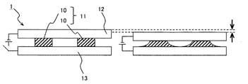
<1.アクチュエータの構成>
図1は、本発明の一実施形態である、ゲル層と2つの電極とからなる単位構造を備えるアクチュエータ1の構成と作用とを模式的に表した図である。アクチュエータ1は、ゲル部10を備えるゲル層11と、該ゲル層11を厚さ方向に挟む電極12及び電極13とからなる単位構造を備える。当該アクチュエータ1は、図1に示すように、電圧を印加しない状態においては、2つの電極間のゲル層11が均一な厚さとなっており、厚さ方向に電圧を印加すると、ゲルが変位し、アクチュエータ1の全体の厚さが小さくなる。
このように、アクチュエータ1は、2つの電極12及び13の間に電圧を印加する操作をON−OFFすることにより、変位状態と元の厚さに復帰する状態とを切り替えること
ができる。すなわち、アクチュエータ1は、電圧の印加操作によって厚さ方向に変位するアクチュエータとして作用する。
<1. Actuator configuration>
FIG. 1 is a diagram schematically showing the configuration and operation of an actuator 1 having a unit structure including a gel layer and two electrodes, which is an embodiment of the present invention. The actuator 1 includes a unit structure including a
In this way, the actuator 1 can switch between a displacement state and a state of returning to the original thickness by turning on and off the operation of applying a voltage between the two
電極12が陰極、電極13が陽極である場合、これらの電極間に電圧を印加すると、陰極12からゲル層に電荷が蓄積する。これにより、陽極13の表面で静電気的な吸着作用が生じ、ゲルが陽極近傍でクリープ変形を起こす。図1に示すように、2つの電極間に電圧を印加すると、クリープ変形により、ゲル層11が陽極13に接する側で裾をひくような形態(電極上を這うような形態)となる。印加電圧を除去すると静電気力は消失し、ゲルの弾性によりゲル層は元の状態に復帰する。
本発明では、上記ゲル部の吸着作用により裾状に広がった側の電極(図1の電極13)を「吸着側電極」と称する。
When the
In the present invention, the electrode on the side that spreads like a hem due to the adsorption action of the gel portion (
本発明のゲルアクチュエータは、平面方向でゲル部を電極よりも小さくすることにより、平面方向へゲルが変形し易くなり、従来変位を大きくするために必要であった電極の凹凸を省くことができる。これにより、アクチュエータ全体の厚さを薄くしたり、製造工程を簡素化できたりするだけでなく、任意の平面形状又は曲面構造のアクチュエータを容易に製造することができる。
また、ゲル層に備えられる各ゲル部の平面方向のサイズを小さくすることにより、電圧印加時の変形量を増大させることができ、また、ゲル部の個数を増加させて高分子ゲルの総面積を増大させることにより、復元力を大きくすることができる。
In the gel actuator of the present invention, by making the gel portion smaller than the electrode in the plane direction, the gel is easily deformed in the plane direction, and the unevenness of the electrode, which is conventionally required to increase the displacement, can be eliminated. .. As a result, not only the thickness of the entire actuator can be reduced and the manufacturing process can be simplified, but also an actuator having an arbitrary planar shape or curved structure can be easily manufactured.
Further, by reducing the size of each gel portion provided in the gel layer in the plane direction, the amount of deformation when a voltage is applied can be increased, and the number of gel portions can be increased to increase the total area of the polymer gel. The restoring force can be increased by increasing.
また、ゲル部の平面方向のサイズを小さくすることにより、溶媒の乾燥や加圧成膜において成型が困難であった、大きな面積を有するゲルアクチュエータを容易に製造することができる。
この観点からみたゲル部のサイズの基準は、電圧印加前のゲル部と吸着電極との接触部の(周長/面積)が2mm−1より大きいことである。この条件を満たす最も簡単な構造は、そのゲル部が直径2mm超の円である構造である。より具体的には、「(周長/面積)」とは、(電圧印加前のゲル部と吸着側電極との接触部の周長/電圧印加前のゲル部と吸着側電極との接触部の面積)である。
ここで、(周長/面積)とは、ゲル部の変形に寄与する割合の指標を意味し、当該数値が大きいと、変形に寄与する部分が増大する。
そして、(周長/面積)は、2mm−1より大きいことが必要であるが、2.5mm−1より大きいことが好ましく、3mm−1より大きいことがより好ましく、4mm−1より大きいことが特に好ましい。これは、変形部分が周辺500μm程度であることを考えれば、ほぼ全域が変形する直径1mmの円柱状のゲル部に相当する。また、(周長/面積)は、特段上限を設ける必要はないが、通常400mm−1以下である。
周長や面積は、ゲル部断面の寸法測定やCTスキャン等を用いることにより測定することができる。もし異なる形状、大きさのものが多数存在する場合には、画像処理により、平均面積と平均周長を求めればよい。
また、(周長/面積)が上記範囲を満たしていれば、本発明の効果を阻害しない範囲で、アクチュエータ全体の一部に、(周長/面積)が上記の範囲よりも小さいゲル部を、少数(例えば個数で全体の2割以下程度)含んでいてもよい。
さらに、平面の高さ方向に変形することを出力とするゲルアクチュエータにおいて、面内での出力を不均等としたい場合(あるいは負荷が面方向で均等でない場合)、ゲル部の位置、分布密度、経分布を調整することにより、所望の変位出力を容易に発生させることができる。
Further, by reducing the size of the gel portion in the plane direction, it is possible to easily manufacture a gel actuator having a large area, which is difficult to mold in drying the solvent or forming a pressure film.
From this point of view, the standard of the size of the gel part is that the (perimeter / area) of the contact part between the gel part and the adsorption electrode before applying the voltage is larger than 2 mm -1 . The simplest structure that satisfies this condition is a structure in which the gel portion is a circle having a diameter of more than 2 mm. More specifically, "(perimeter / area)" means (perimeter of the contact portion between the gel portion before applying the voltage and the adsorption side electrode / the contact portion between the gel portion before applying the voltage and the adsorption side electrode. Area).
Here, (perimeter / area) means an index of the ratio that contributes to the deformation of the gel portion, and when the value is large, the portion that contributes to the deformation increases.
The (perimeter / area) needs to be larger than 2 mm -1 , but is preferably larger than 2.5 mm -1, more preferably larger than 3 mm -1 , and larger than 4 mm -1. Especially preferable. Considering that the deformed portion has a peripheral circumference of about 500 μm, this corresponds to a columnar gel portion having a diameter of 1 mm in which almost the entire region is deformed. Further, (perimeter / area) does not need to have a special upper limit, but is usually 400 mm -1 or less.
The circumference and area can be measured by measuring the dimensions of the cross section of the gel portion, using a CT scan, or the like. If there are many different shapes and sizes, the average area and average circumference may be obtained by image processing.
Further, if (perimeter / area) satisfies the above range, a gel portion having (perimeter / area) smaller than the above range is formed on a part of the entire actuator within a range that does not impair the effect of the present invention. , A small number (for example, about 20% or less of the total number) may be included.
Furthermore, in a gel actuator whose output is to deform in the height direction of a plane, when it is desired to make the output in the plane uneven (or when the load is not uniform in the plane direction), the position of the gel portion, the distribution density, By adjusting the meridian distribution, a desired displacement output can be easily generated.
上述した、ゲル部の平面方向のサイズを小さくすることにより、溶媒の乾燥や加圧成膜において成型が困難であった、大きな面積を有するゲルアクチュエータを容易に製造することができる観点からみたゲル部のサイズの基準の指標としては、(周長/面積)以外に
も、電圧印加前のゲル部と吸着側電極との接触部の(1/面積)が挙げられる。この場合、(1/面積)が0.32mm−2より大きいことが好ましい。この条件を満たす最も簡単な構造は、そのゲル部が直径2mm超の円である構造である。より具体的には、「(1/面積)」とは、(1/電圧印加前のゲル部と吸着側電極との接触部の面積)である。
ここで、(1/面積)とは、ゲル部1つ当たりの接触面積の逆数を意味し、当該数値が大きいと、変形量や復元力が大きくなる。
そして、(1/面積)は、0.32mm−2より大きいことが好ましく、0.5mm−2より大きいことがより好ましく、0.8mm−2より大きいことがさらに好ましく、1.27mm−2より大きいことが特に好ましい。これは、変形部分が周辺500μm程度であることを考えれば、ほぼ全域が変形する直径1mmの円柱状のゲル部に相当する。また、(1/面積)は、特段上限を設ける必要はないが、通常10000mm−2以下、好ましくは100mm−2以下である。
面積は、ゲル部断面の寸法測定やCTスキャン等を用いることにより測定することができる。もし異なる形状、大きさのものが多数存在する場合には、画像処理により、平均面積と平均周長を求めればよい。
また、(1/面積)が上記範囲を満たしていれば、本発明の効果を阻害しない範囲で、アクチュエータ全体の一部に、(1/面積)が上記の範囲よりも小さいゲル部を、少数(例えば個数で全体の2割以下程度)含んでいてもよい。
さらに、平面の高さ方向に変形することを出力とするゲルアクチュエータにおいて、面内での出力を不均等としたい場合(あるいは負荷が面方向で均等でない場合)、ゲル部の位置、分布密度、経分布を調整することにより、所望の変位出力を容易に発生させることができる。
By reducing the size of the gel portion in the plane direction as described above, a gel from the viewpoint that a gel actuator having a large area, which is difficult to mold in solvent drying or pressure film formation, can be easily manufactured. In addition to (perimeter / area), the index of the standard for the size of the part includes (1 / area) of the contact part between the gel part and the adsorption side electrode before applying the voltage. In this case, it is preferable that (1 / area) is larger than 0.32 mm- 2 . The simplest structure that satisfies this condition is a structure in which the gel portion is a circle having a diameter of more than 2 mm. More specifically, "(1 / area)" is (1 / area of the contact portion between the gel portion and the adsorption side electrode before voltage application).
Here, (1 / area) means the reciprocal of the contact area per gel portion, and the larger the value, the larger the deformation amount and the restoring force.
Then, (1 / area) is preferably larger than 0.32 mm -2, and more preferably greater than 0.5 mm -2, more preferably greater than 0.8 mm -2, from 1.27 mm -2 Larger is particularly preferable. Considering that the deformed portion has a peripheral circumference of about 500 μm, this corresponds to a columnar gel portion having a diameter of 1 mm in which almost the entire region is deformed. Further, (1 / area) does not need to have a special upper limit, but is usually 10000 mm- 2 or less, preferably 100 mm- 2 or less.
The area can be measured by measuring the dimensions of the cross section of the gel portion, using a CT scan, or the like. If there are many different shapes and sizes, the average area and average circumference may be obtained by image processing.
Further, if (1 / area) satisfies the above range, a small number of gel portions having (1 / area) smaller than the above range are provided in a part of the entire actuator within a range that does not impair the effect of the present invention. (For example, the number may be about 20% or less of the total).
Furthermore, in a gel actuator whose output is to deform in the height direction of a plane, when it is desired to make the output in the plane uneven (or when the load is not uniform in the plane direction), the position of the gel portion, the distribution density, By adjusting the meridian distribution, a desired displacement output can be easily generated.
以下、ゲル層に備えられるゲル部の態様について具体的に説明する。以下で説明する形状や大きさ等の特性について、ゲル層に備えられる複数のゲル部の態様は、同じであっても、異なっていてもよい。また、上述した通り、「ゲル部」に関する特性値は、特段の断りがない限り、ゲル層に備えられる複数のゲル部の各々の特性値の平均値として算出する。 Hereinafter, the mode of the gel portion provided in the gel layer will be specifically described. Regarding the characteristics such as the shape and size described below, the modes of the plurality of gel portions provided in the gel layer may be the same or different. Further, as described above, the characteristic value relating to the "gel portion" is calculated as an average value of the characteristic values of each of the plurality of gel portions provided in the gel layer, unless otherwise specified.
ゲル層に備えられるゲル部の形状は、周囲に変形を逃がす隙間があれば特段限定されず、用途に応じて任意に設計でき、例えば、島状(ドット状)、線状、ドーナツ状とすることができる。これらの中でも、基板に転写が可能な印刷技術により、ゲル層形成を効率的に生産が可能になる観点から、角柱状、円柱状等の島状であることが好ましく、特に、印加電圧による変形が均一であるために変位量を大きくすることができる観点から、円柱状であることが好ましい。円柱状の場合、周方向に均一に変形するため、耐久性がよいという効果もある。但し、凹多角形及び凹曲線面を持つ形状(例えば星形など)の場合に関しては、凸多角形及び凸曲線面を持つ形状(例えば円、楕円、凸型多角形など)に比べ周囲の長さが長く、電場が集中しやすく有利に働くので、変形量や発生力などの観点から有利である。 The shape of the gel portion provided in the gel layer is not particularly limited as long as there is a gap around it to allow deformation to escape, and can be arbitrarily designed according to the application. For example, it may be island-shaped (dot-shaped), linear, or donut-shaped. be able to. Among these, from the viewpoint of efficiently producing the gel layer formation by the printing technology capable of transferring to the substrate, it is preferable to have an island shape such as a prismatic shape or a columnar shape, and in particular, deformation due to an applied voltage. It is preferable that the columnar shape is used from the viewpoint that the amount of displacement can be increased because of the uniformity. In the case of a columnar shape, it is deformed uniformly in the circumferential direction, so that it also has an effect of good durability. However, in the case of a shape having a concave polygon and a concave curved surface (for example, a star shape), the circumference is longer than that of a shape having a convex polygon and a convex curved surface (for example, a circle, an ellipse, a convex polygon, etc.). Since the polygon is long and the electric field is easily concentrated and works advantageously, it is advantageous from the viewpoint of the amount of deformation and the generated force.
電圧印加前における、ゲル部の厚さは、特段限定されず、用途や電極の面積に応じて任意に設計し得るが、アクチュエータとして変形する挙動の実用上の観点から、通常1μm以上であり、好ましくは2μm以上であり、より好ましくは3μm以上であり、特に好ましくは5μm以上であり、最も好ましくは10μm以上であり、一方で、通常10mm以下であり、好ましくは5mm以下であり、より好ましくは1mm以下であり、特に好ましくは0.6mm以下であり、最も好ましくは0.2mm以下である。 The thickness of the gel portion before applying a voltage is not particularly limited and can be arbitrarily designed according to the application and the area of the electrode, but it is usually 1 μm or more from the practical viewpoint of the behavior of deforming as an actuator. It is preferably 2 μm or more, more preferably 3 μm or more, particularly preferably 5 μm or more, most preferably 10 μm or more, while usually 10 mm or less, preferably 5 mm or less, more preferably. It is 1 mm or less, particularly preferably 0.6 mm or less, and most preferably 0.2 mm or less.
電圧印加前における、ゲル部と吸着側電極との接触部の周長は、特段限定されず、用途や電極の面積に応じて任意に設計し得るが、ゲルの周長部分が変形の寄与するための電極とゲル部との接触部の面積を確保する観点から、通常0.01mm以上であり、好ましく
は0.05mm以上であり、より好ましくは0.1mm以上であり、特に好ましくは0.5mm以上であり、最も好ましくは1mm以上である。一方で、上限については特段設定する必要はないが、通常10mm以下である。
The peripheral length of the contact portion between the gel portion and the adsorption side electrode before applying the voltage is not particularly limited and can be arbitrarily designed according to the application and the area of the electrode, but the peripheral length portion of the gel contributes to the deformation. From the viewpoint of securing the area of the contact portion between the electrode and the gel portion, it is usually 0.01 mm or more, preferably 0.05 mm or more, more preferably 0.1 mm or more, and particularly preferably 0. It is 5 mm or more, and most preferably 1 mm or more. On the other hand, the upper limit does not need to be set in particular, but is usually 10 mm or less.
電圧印加前における、ゲル層と吸着側電極との平均接触面積は、電極の面積よりも小さければ特段限定されず、用途や電極の面積に応じて任意に設計し得るが、ゲル部の平面方向のサイズを小さくすることにより、溶媒の乾燥や加圧成膜において成型が困難であった、大きな面積を有するゲルアクチュエータを容易に製造することができる観点から、3.14mm2未満であることが好ましく、2mm2以下であることがより好ましく、1.25mm2以下であることがさらに好ましく、0.79mm2以下であることが特に好ましい。一方で、特段下限を設ける必要はないが、通常0.0001mm2以上であり、好ましくは0.01mm2以上である。
また、ゲル部と電圧印加前の吸着側電極との接触面積は、ゲル層に備えられる全てのゲル部が同一であってもよいが、異なっていてもよく、複数のゲルの島の設置場所に応じてゲルの体積や電極との接触面積を変化させることにより、設置場所に応じて不均一な力が必要となる場合に対応しやすくなる。
The average contact area between the gel layer and the adsorption side electrode before applying the voltage is not particularly limited as long as it is smaller than the electrode area, and can be arbitrarily designed according to the application and the electrode area, but in the plane direction of the gel portion. By reducing the size of the gel actuator, it is possible to easily manufacture a gel actuator having a large area, which was difficult to mold in drying the solvent or forming a pressure film, and the size is less than 3.14 mm 2. preferably, more preferably 2 mm 2 or less, further preferably 1.25 mm 2 or less, particularly preferably 0.79 mm 2 or less. On the other hand, it is not necessary to provide a special lower limit is usually 0.0001 mm 2 or more, preferably 0.01 mm 2 or more.
Further, the contact area between the gel portion and the adsorption side electrode before applying the voltage may be the same for all the gel portions provided in the gel layer, but may be different, and the installation locations of a plurality of gel islands. By changing the volume of the gel and the contact area with the electrode according to the above conditions, it becomes easier to deal with the case where a non-uniform force is required depending on the installation location.
吸着側電極の面積に対する、電圧印加前のゲル部と吸着側電極との接触面積の割合は、特段限定されず、用途や電極の面積に応じて任意に設計し得るが、供給電力効率の観点から、通常1%以上であり、好ましくは3%以上であり、より好ましくは5%以上であり、さらに好ましくは10%以上であり、特に好ましくは15%以上であり、一方で、通常100%以下であり、好ましくは90%以下であり、より好ましくは80%以下であり、さらに好ましくは70%以下であり、特に好ましくは60%以下である。 The ratio of the contact area between the gel portion and the suction side electrode before applying the voltage to the area of the suction side electrode is not particularly limited and can be arbitrarily designed according to the application and the electrode area, but from the viewpoint of power supply efficiency. Therefore, it is usually 1% or more, preferably 3% or more, more preferably 5% or more, further preferably 10% or more, particularly preferably 15% or more, while usually 100%. It is less than or equal to 90% or less, more preferably 80% or less, still more preferably 70% or less, and particularly preferably 60% or less.
電圧印加前のゲル部と吸着側電極との接触面積に対する、電圧(設計上の最大電圧)印加後のゲル部と吸着側電極との接触面積の割合は、特段限定されず、用途や電極の面積に応じて任意に設計し得るが、供給電力効率の観点から、通常100%以上であり、好ましくは102%以上であり、より好ましくは105%以上であり、さらに好ましくは110%以上であり、特に好ましくは120%以上であり、一方で、通常300%以下であり、好ましくは250%以下であり、より好ましくは200%以下であり、さらに好ましくは180%以下であり、特に好ましくは160%以下である。 The ratio of the contact area between the gel part and the adsorption side electrode after applying the voltage (maximum design voltage) to the contact area between the gel part and the adsorption side electrode before applying the voltage is not particularly limited, and the application and the electrode It can be arbitrarily designed according to the area, but from the viewpoint of power supply efficiency, it is usually 100% or more, preferably 102% or more, more preferably 105% or more, and further preferably 110% or more. , Especially preferably 120% or more, on the other hand, usually 300% or less, preferably 250% or less, more preferably 200% or less, still more preferably 180% or less, particularly preferably 160. % Or less.
ゲル層に備えられるゲル部の数は、複数であれば特段限定されず、用途や電極の面積に応じて任意に設計し得るが、均等な変形を促すための観点から、通常2以上であり、好ましくは25以上であり、より好ましくは100以上であり、特に好ましくは200以上であり、最も好ましくは10000以上であり、一方で、通常100000以下であり、好ましくは10000以下であり、より好ましくは5000以下であり、特に好ましくは1000以下であり、最も好ましくは500以下である。
なお、複数の島は、規則的に配置されてよく、不規則であってよい。また、複数の島は同一の大きさであってよく、異なってもよい。
The number of gel portions provided in the gel layer is not particularly limited as long as it is plural, and can be arbitrarily designed according to the application and the area of the electrodes, but is usually 2 or more from the viewpoint of promoting uniform deformation. , Is preferably 25 or more, more preferably 100 or more, particularly preferably 200 or more, most preferably 10000 or more, while usually 100,000 or less, preferably 10000 or less, more preferably. Is 5000 or less, particularly preferably 1000 or less, and most preferably 500 or less.
The plurality of islands may be arranged regularly and may be irregular. Also, the plurality of islands may be the same size or may be different.
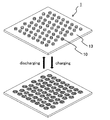
ゲル部の配置は、特段限定されず、用途や電極の面積に応じて任意に設計し得るが、変形したゲルの逃げで最大の変形を得るための観点から、図2に示すように、ゲル部の設計上の最大変形時においても、隣接するゲル部に接触しないような間隔を空けることが好ましい。なお、当該図2では、アクチュエータの上面の電極や、外部の電源、スイッチの記載を省略した。
設計上の最大変形時とは、アクチュエータの設計時に設定される、変形が最も大きくなる状態であり、通常は設計上の最大電圧を印加した時の変形量である。
The arrangement of the gel portion is not particularly limited and can be arbitrarily designed according to the application and the area of the electrode. However, from the viewpoint of obtaining the maximum deformation by the escape of the deformed gel, the gel is as shown in FIG. It is preferable to leave a space so as not to come into contact with the adjacent gel portion even at the time of maximum deformation of the portion in design. In FIG. 2, the description of the electrodes on the upper surface of the actuator, the external power supply, and the switch is omitted.
The design maximum deformation is the state in which the deformation is the largest, which is set at the time of designing the actuator, and is usually the amount of deformation when the design maximum voltage is applied.
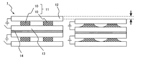
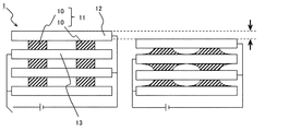
単位構造であるアクチュエータは、単独で用いる、又は厚さ方向に複数個重ね合せて作
製した積層型で用いることができる。積層型で用いる場合、図3に示すように、隣接するアクチュエータの間に絶縁層を備えて積層させる態様、また、図4に示すように、隣接するアクチュエータの間にゲル層を備えて積層させる態様とすることができる。
なお、アクチュエータと電源やスイッチとの接続の態様は、特段制限されず、積層型の場合、例えば、図3に示すように、単位構造であるアクチュエータ毎に電源やスイッチを設けて接続する態様、また、図4に示すように、積層された単位構造であるアクチュエータの各々の電極に接続された導線を一つの電源やスイッチに接続させ、一つのスイッチのON−OFFで複数のゲルの変位を制御するような態様とすることができる。
上記の絶縁層の種類は、特段限定されず、例えば、シリコンの熱酸化膜(SiO2)、Si3N4、ZrO2、Y2O3、ZnO、Al2O3等を用いることができる。また、絶縁層の厚さは、用途に応じて適宜選択することができるが、良好な絶縁性を保持しつつ小型化を可能とする観点から、通常10nm〜10mmであり、好ましくは1μm〜5mmである。
なお、積層型のアクチュエータにおいて、該アクチュエータを構成する各部材の特性は、積層型アクチュエータ全体で評価してもよく、ゲル層と該ゲル層を厚さ方向に挟む陽極及び陰極とからなる単位構造ごとに評価してもよい。
The actuator having a unit structure can be used alone or in a laminated type manufactured by stacking a plurality of actuators in the thickness direction. When used in a laminated type, as shown in FIG. 3, an insulating layer is provided between adjacent actuators for lamination, and as shown in FIG. 4, a gel layer is provided between adjacent actuators for lamination. It can be an embodiment.
The mode of connection between the actuator and the power supply or switch is not particularly limited, and in the case of the laminated type, for example, as shown in FIG. 3, a mode in which a power supply or switch is provided for each actuator having a unit structure and connected. Further, as shown in FIG. 4, the lead wires connected to each electrode of the actuator, which is a laminated unit structure, are connected to one power supply or switch, and the displacement of a plurality of gels is changed by turning on and off one switch. The mode can be controlled.
The type of the above-mentioned insulating layer is not particularly limited, and for example, a silicon thermal oxide film (SiO 2 ), Si 3 N 4 , ZrO 2 , Y 2 O 3 , ZnO, Al 2 O 3 and the like can be used. .. The thickness of the insulating layer can be appropriately selected depending on the application, but is usually 10 nm to 10 mm, preferably 1 μm to 5 mm from the viewpoint of enabling miniaturization while maintaining good insulating properties. Is.
In the laminated actuator, the characteristics of each member constituting the actuator may be evaluated for the entire laminated actuator, and a unit structure including a gel layer and an anode and a cathode sandwiching the gel layer in the thickness direction. It may be evaluated for each.
アクチュエータ中のゲル層に備えられる複数のゲル部の総重量は、アクチュエータの用途に応じて任意に選択できるが、特にゲル層を複数有するアクチュエータの変位長を確保する観点から、通常10重量%以上であり、好ましくは15重量%以上であり、より好ましくは18重量%以上であり、さらに好ましくは20重量%以上であり、特に好ましくは22重量%以上であり、また、好ましくは50重量%以下であり、より好ましくは45重量%以下であり、さらに好ましくは43重量%以下であり、特に好ましくは40重量%以下である。
アクチュエータ全体の厚さに対するゲル層の厚さの割合は、アクチュエータの用途に応じて任意に選択できるが、通常0.1から99.98%であり、1〜95%であることが好ましく、5〜90%であることがより好ましく、10〜85%であることがさらに好ましい。上記の下限以上とすることにより、無課電状態でゲル層がメッシュ等の隙間に入り込んでしまうことにより、変位長が小さくなる影響を小さくできるため好ましく、また、上記の上限以下とすることにより、メッシュとの接触確率を十分に維持でき、変位に必要な電圧を低くすることができる。
The total weight of the plurality of gel portions provided in the gel layer in the actuator can be arbitrarily selected according to the application of the actuator, but is usually 10% by weight or more from the viewpoint of ensuring the displacement length of the actuator having a plurality of gel layers. It is preferably 15% by weight or more, more preferably 18% by weight or more, further preferably 20% by weight or more, particularly preferably 22% by weight or more, and preferably 50% by weight or less. It is more preferably 45% by weight or less, further preferably 43% by weight or less, and particularly preferably 40% by weight or less.
The ratio of the thickness of the gel layer to the total thickness of the actuator can be arbitrarily selected depending on the application of the actuator, but is usually 0.1 to 99.98%, preferably 1 to 95%. It is more preferably ~ 90%, and even more preferably 10-85%. By setting it above the above lower limit, it is preferable that the gel layer enters the gaps of the mesh or the like in a non-charged state, so that the effect of reducing the displacement length can be reduced, and by setting it below the above upper limit. , The contact probability with the mesh can be sufficiently maintained, and the voltage required for displacement can be lowered.
<2.ゲル層>
<2−1.ゲル部の原料>
ゲル層に備えられるゲル部は、誘電性高分子材料を含んでいれば、特段限定されず、以下に示す態様以外だけでなく、特開2012−23843号公報や特開2014−32152号公報等に開示されるゲルの原料を用いることができる。また、ゲル層が備える複数のゲル部の材料は、同じであっても、異なっていてもよいが、印加電圧による変化量を均一にできる観点から、同じであることが好ましい。
ゲル部材料は、電気刺激により屈曲変形やクリープ変形をなし、また、電位差をかけると収縮する材料である。ゲル部に含まれる誘電性高分子材料としては、例えば、ポリ塩化ビニル、ポリビニルブチラール、ポリメタクリル酸メチル、ポリウレタン、ポリスチレン、ポリ酢酸ビニル、ナイロン6、ポリビニルアルコール、ポリカーボネイト、ポリエチレンテレフタレート、及びポリアクリロニトリル、シリコーンゴム等を用いることができる。これらの中でも、印加電圧による変位量や発生力がより大きく出力される物質の観点から、ポリ塩化ビニル及びポリビニルブチラールが好ましい。これらの誘電性高分子材料の製法は、特段限定されず、一般に市販されているものを用いることができる。
<2. Gel layer>
<2-1. Raw material for gel part>
The gel portion provided in the gel layer is not particularly limited as long as it contains a dielectric polymer material, and is not limited to the embodiments shown below, as well as JP-A-2012-23843, JP-A-2014-32152, and the like. The raw material of the gel disclosed in the above can be used. Further, the materials of the plurality of gel portions provided in the gel layer may be the same or different, but are preferably the same from the viewpoint that the amount of change due to the applied voltage can be made uniform.
The gel part material is a material that undergoes bending deformation or creep deformation due to electrical stimulation, and contracts when a potential difference is applied. Examples of the dielectric polymer material contained in the gel portion include polyvinyl chloride, polyvinyl butyral, polymethyl methacrylate, polyurethane, polystyrene, polyvinyl acetate, nylon 6, polyvinyl alcohol, polycarbonate, polyethylene terephthalate, and polyacrylonitrile. Silicone rubber or the like can be used. Among these, polyvinyl chloride and polyvinyl butyral are preferable from the viewpoint of a substance that outputs a larger amount of displacement and generated force due to the applied voltage. The method for producing these dielectric polymer materials is not particularly limited, and generally commercially available materials can be used.
ゲル部中の誘電性高分子材料の含有量は、特段制限されないが、ゲルの変位長が十分得られる観点から、通常5重量%以上であり、好ましくは8重量%以上であり、より好まし
くは10重量%以上であり、さらに好ましくは12重量%以上であり、特に好ましくは15重量%以上であり、また、好ましくは60重量%以下であり、より好ましくは50重量%以下であり、さらに好ましくは45重量%以下であり、特に好ましくは40重量%以下である。
The content of the dielectric polymer material in the gel portion is not particularly limited, but is usually 5% by weight or more, preferably 8% by weight or more, more preferably 8% by weight or more, from the viewpoint of obtaining a sufficient displacement length of the gel. It is 10% by weight or more, more preferably 12% by weight or more, particularly preferably 15% by weight or more, preferably 60% by weight or less, more preferably 50% by weight or less, still more preferable. Is 45% by weight or less, and particularly preferably 40% by weight or less.
誘電性高分子材料として、ポリ塩化ビニルを用いる場合、その数平均分子量(Mn)は、特段制限されないが、電圧印加時の変位量を向上させる観点から、ゲル浸透クロマトグラフィー(GPC)により測定したポリスチレン換算で、7万以上20万以下であるが、好ましくは7.5万以上であり、より好ましくは8万以上であり、さらに好ましくは8.5万以上であり、特に好ましくは9万以上であり、また、好ましくは18万以下であり、より好ましくは16万以下であり、さらに好ましくは14万以下であり、特に好ましくは12万以下である。ポリ塩化ビニルの数平均分子量(Mn)を7万以上とすることで得ら
れたゲルが経時的に変化し電気的特性が安定しやすくなる。一方20万以下とすることにより、得られたゲルが固くなりすぎず、電圧をかけた時の変位長が十分に得られる。
When polyvinyl chloride is used as the conductive polymer material, its number average molecular weight (Mn) is not particularly limited, but it is measured by gel permeation chromatography (GPC) from the viewpoint of improving the displacement amount when a voltage is applied. In terms of polystyrene, it is 70,000 or more and 200,000 or less, preferably 75,000 or more, more preferably 80,000 or more, further preferably 85,000 or more, and particularly preferably 90,000 or more. It is preferably 180,000 or less, more preferably 160,000 or less, still more preferably 140,000 or less, and particularly preferably 120,000 or less. By setting the number average molecular weight (Mn) of polyvinyl chloride to 70,000 or more, the obtained gel changes with time and the electrical characteristics become easy to stabilize. On the other hand, when the amount is 200,000 or less, the obtained gel does not become too hard, and a sufficient displacement length when a voltage is applied can be obtained.
また、誘電性高分子材料として、ポリビニルブチラールを用いる場合、その数平均分子量(Mn)電圧印加時の変位量を向上させる観点から、6万以上15万以下であるが、好ましくは7万以上であり、より好ましくは8万以上であり、また、好ましくは14万以下であり、より好ましくは13万以下である。ポリビニルブチラールの数平均分子量を上述のそれぞれの数平均分子量以上とすることで、連続したシート化を容易にすることができ、取り扱いが容易になる。一方上述のそれぞれの数平均分子量以下とすることで、適度な硬度となり、電圧に対する変位長を十分に確保できる。
なお、ここでいう数平均分子量は、GPC(ゲル浸透クロマトグラフィー)によるポリ
スチレン換算の値を用いる。また市販品を使用する場合には、使用する製品によっては数平均分子量ではなく、計算分子量が記載されていることがあるが、数平均分子量と計算分子量は実質的に同様の値になるため、計算分子量も同様の範囲で用いることができる。
When polyvinyl butyral is used as the dielectric polymer material, it is 60,000 or more and 150,000 or less, preferably 70,000 or more, from the viewpoint of improving the displacement amount when a number average molecular weight (Mn) voltage is applied. Yes, more preferably 80,000 or more, preferably 140,000 or less, and more preferably 130,000 or less. By setting the number average molecular weight of polyvinyl butyral to be equal to or higher than the above-mentioned number average molecular weights, continuous sheet formation can be facilitated and handling becomes easy. On the other hand, by setting the molecular weight to each of the above-mentioned number averages or less, the hardness becomes appropriate and the displacement length with respect to the voltage can be sufficiently secured.
The number average molecular weight referred to here is a polystyrene-equivalent value obtained by GPC (gel permeation chromatography). When using a commercially available product, the calculated molecular weight may be described instead of the number average molecular weight depending on the product used. However, since the number average molecular weight and the calculated molecular weight are substantially the same, The calculated molecular weight can be used in the same range.
ゲル部は、本発明の効果が発揮される範囲において、上記の誘電性高分子材料以外の材料を含んでいてもよく、例えば、可塑剤や電荷補足剤等が挙げられる。 The gel portion may contain a material other than the above-mentioned dielectric polymer material as long as the effect of the present invention is exhibited, and examples thereof include a plasticizer and a charge-capturing agent.
可塑剤の種類は、特段限定されないが、例えば、ジオールジエステル、ジカルボン酸ジエステル、ジメチルアセトアミド(DMA)、ジエタノールアミン(DEA)等が挙げられる。ジカルボン酸エステルとしては、例えばアジピン酸ジブチル(DBA)、セバシン酸ジオクチル(DOS)、アジピン酸ジオクチル(DOA)、フタル酸ジメチル(DMP)、フタル酸ジブチル(DBP)、フタル酸ジオクチル(DOP)、フタル酸ビス(2-エチルヘキシル)(DEHP)、コハク酸ジエチル(DESuc)、アジピン酸ジメチル(DMA)、セバシン酸ジ
エチル(DESeb)、セバシン酸ジブチル(DBSeb)、セバシン酸ジオクチル(DOS
eb)等が挙げられる。これらの中でも、比較的取扱いやすく安定なゲル物質を得るため
の観点から、ジオールジエステル及びジカルボン酸ジエステルが好ましく、特に、誘電性高分子としてポリ塩化ビニルを用いた場合にはジオールジエステルやジカルボン酸ジエステルを用いることが好ましく、また、誘電性高分子としてポリビニルブチラールを用いた場合にはジカルボン酸ジエステルを用いることが好ましい。これらの誘電性高分子材料の製法は、特段限定されず、一般に市販されているものを用いることができる。
The type of plasticizer is not particularly limited, and examples thereof include diol diester, dicarboxylic acid diester, dimethylacetamide (DMA), and diethanolamine (DEA). Examples of the dicarboxylic acid ester include dibutyl adipate (DBA), dioctyl sebacate (DOS), dioctyl adipate (DOA), dimethyl phthalate (DMP), dibutyl phthalate (DBP), dioctyl phthalate (DOP), and phthalate. Bis (2-ethylhexyl) acid (DEHP), diethyl succinate (DESuc), dimethyl adipate (DMA), diethyl sevacinate (DESeb), dibutyl sevacinate (DBSeb), dioctyl sevacinate (DOS)
eb) and the like. Among these, diol diesters and dicarboxylic acid diesters are preferable from the viewpoint of obtaining a gel substance that is relatively easy to handle and stable, and in particular, when polyvinyl chloride is used as the dielectric polymer, diol diesters and dicarboxylic acid diesters are used. When polyvinyl butyral is used as the dielectric polymer, it is preferable to use a dicarboxylic acid diester. The method for producing these dielectric polymer materials is not particularly limited, and generally commercially available materials can be used.
ゲル部中の可塑剤の含有量は、特段制限されないが、良好な変位長の発現とゲル表面のべたつき抑制の観点から、通常55重量%以上であり、好ましくは60重量%以上であり、より好ましくは65重量%以上であり、さらに好ましくは70重量%以上であり、特に好ましくは75重量%以上であり、また、好ましくは95重量%以下であり、より好ましくは93重量%以下であり、さらに好ましくは90重量%以下であり、特に好ましくは85重量%以下である。 The content of the plasticizer in the gel portion is not particularly limited, but is usually 55% by weight or more, preferably 60% by weight or more, more preferably, from the viewpoint of developing a good displacement length and suppressing stickiness on the gel surface. It is preferably 65% by weight or more, more preferably 70% by weight or more, particularly preferably 75% by weight or more, and preferably 95% by weight or less, more preferably 93% by weight or less. It is more preferably 90% by weight or less, and particularly preferably 85% by weight or less.
電荷補足剤の種類は、特段限定されないが、例えば、テトラシアノキノジメタン、2,4,7−トリニトロフルオレン−9−オンが挙げられる。 The type of charge-replenishing agent is not particularly limited, and examples thereof include tetracyanoquinodimethane and 2,4,7-trinitrofluorene-9-one.
ゲル部中の電荷補足剤の含有量は、特段制限されないが、良好な変位長の発現の観点から、通常0.01重量%以上であり、好ましくは0.02重量%以上であり、より好ましくは0.03重量%以上であり、さらに好ましくは0.05重量%以上であり、特に好ましくは0.1重量%以上であり、また、好ましくは10重量%以下であり、より好ましくは5重量%以下であり、さらに好ましくは3重量%以下であり、特に好ましくは2重量%以下である。 The content of the charge catching agent in the gel portion is not particularly limited, but is usually 0.01% by weight or more, preferably 0.02% by weight or more, more preferably, from the viewpoint of developing a good displacement length. Is 0.03% by weight or more, more preferably 0.05% by weight or more, particularly preferably 0.1% by weight or more, and preferably 10% by weight or less, more preferably 5% by weight. % Or less, more preferably 3% by weight or less, and particularly preferably 2% by weight or less.
ゲル部の密度は、通常0.7〜1.5g/cm3であり、0.8〜1.4g/cm3であることが好ましく、0.85〜1.35g/cm3であることがより好ましい。
ゲル部の密度が上記範囲内であると、厚みが薄くなっても荷重を支えることが可能であり、厚みが厚くなってもアクチュエータの重量の増加を抑えることが可能であるという利点がある。なお、測定方法については、一般的な密度の測定方法を適用できる。
The density of the gel portion is generally 0.7~1.5g / cm 3, is preferably 0.8 to 1.4 g / cm 3, to be 0.85~1.35g / cm 3 More preferred.
When the density of the gel portion is within the above range, there is an advantage that the load can be supported even if the thickness becomes thin, and the increase in the weight of the actuator can be suppressed even if the thickness becomes thick. As the measuring method, a general density measuring method can be applied.
<2−2.ゲル部の製造方法>
ゲル部の製造方法は、特段限定されず、特開2012−23843号公報や特開2014−32152号公報等に開示される一般的なゲルの製造方法により製造することができ、例えば、上述した各種原料に溶媒を加えた混合溶液を調製し、当該混合溶液をテフロン(登録商標)製シャーレ等の離型性のよい容器に移し、一定時間静置してゲル化させた後、容器から剥離することでゲル部を得ることができる。
<2-2. Gel part manufacturing method>
The method for producing the gel portion is not particularly limited, and the gel portion can be produced by a general gel manufacturing method disclosed in JP-A-2012-23843, JP-A-2014-32152, etc., for example, as described above. Prepare a mixed solution in which a solvent is added to various raw materials, transfer the mixed solution to a container with good releasability such as a petri dish manufactured by Teflon (registered trademark), leave it to stand for a certain period of time to gel it, and then peel it off from the container. The gel part can be obtained by doing so.
ゲル部を製造する際に用いられる溶媒の種類は、上記のポリビニルブチラール及びジカルボン酸ジエステル化合物を溶解させるものであれば特段制限されないが、例えば、メタノール、エタノール、n−ブタノール、n−プロパノール、イソプロパノール等のアルコール系溶媒、テトラヒドロフラン、1,4−ジオキサン等のエーテル系溶媒、メチルセロソルブ、エチルセロソルブ等のセロソルブ系溶媒、N,N−ジメチルホルムアミド、N,N−ジメチルアセトアミド、N−メチルピロリドン等のアミド系溶媒、アセトニトリル等のニトリル系溶媒等の有機溶媒が挙げられる。これらは1種を単独で用いても、2種以上を併用してもよい。これらの中でも、テトラヒドロフラン、イソプロパノール、及びメタノールが好ましく、特に、揮発性と臭気の観点から、テトラヒドロフランであることが好ましい。 The type of solvent used in producing the gel portion is not particularly limited as long as it dissolves the above-mentioned polyvinyl butyral and dicarboxylic acid diester compounds, and for example, methanol, ethanol, n-butanol, n-propanol and isopropanol. Alcohol-based solvents such as tetrahydrofuran, ether-based solvents such as 1,4-dioxane, cellosolve-based solvents such as methyl cellosolve and ethyl cellosolve, N, N-dimethylformamide, N, N-dimethylacetamide, N-methylpyrrolidone and the like. Examples thereof include amide solvents and organic solvents such as nitrile solvents such as acetonitrile. These may be used alone or in combination of two or more. Among these, tetrahydrofuran, isopropanol, and methanol are preferable, and tetrahydrofuran is particularly preferable from the viewpoint of volatility and odor.
溶媒を揮発させる前の組成物中の溶媒の含有量は、溶解速度と揮発速度の観点から、通常40重量%以上であり、好ましくは45重量%以上であり、より好ましくは50重量%以上であり、さらに好ましくは55重量%以上であり、特に好ましくは60重量%以上であり、また、好ましくは98重量%以下であり、より好ましくは95重量%以下であり、さらに好ましくは90重量%以下であり、特に好ましくは85重量%以下である。 The content of the solvent in the composition before volatilizing the solvent is usually 40% by weight or more, preferably 45% by weight or more, and more preferably 50% by weight or more from the viewpoint of dissolution rate and volatilization rate. Yes, more preferably 55% by weight or more, particularly preferably 60% by weight or more, still preferably 98% by weight or less, more preferably 95% by weight or less, still more preferably 90% by weight or less. It is particularly preferably 85% by weight or less.
<3.電極>
前記ゲル層を厚さ方向に挟む陽極と陰極(これらをまとめて「2つの電極」とも称す)の形状は、特段制限されず、電圧の印加により変位したゲルが移動できる空間がある形状であってもよく、また、当該空間がない形状であってもよい。電圧の印加により変位したゲルが移動できる空間がある形状とは、例えば、電極の一部に切欠きを有する形状、凹凸を有する形状、網状の形状等が挙げられる。
上記の空間がある形状の場合、アクチュエータ全体の厚さを薄くすることができず、アクチュエータの大きさに対する変形量が小さくなってしまうため、空間がない形状である方が好ましい。
また、以下に示す電極の厚さや材料の種類は、陽極と陰極で同じであっても、異なっていてもよい。
<3. Electrode>
The shapes of the anode and cathode (collectively referred to as "two electrodes") that sandwich the gel layer in the thickness direction are not particularly limited, and there is a space in which the displaced gel can move due to the application of voltage. It may be a shape without the space. Examples of the shape having a space in which the gel displaced by the application of voltage can move include a shape having a notch in a part of the electrode, a shape having unevenness, and a net-like shape.
In the case of a shape having the above space, the thickness of the entire actuator cannot be reduced and the amount of deformation with respect to the size of the actuator becomes small. Therefore, the shape without the space is preferable.
Further, the thickness of the electrodes and the type of material shown below may be the same or different between the anode and the cathode.
電極の厚さは、アクチュエータの用途に応じて任意に選択でき、通常0.01〜1mmであり、0.012〜0.9mmであることが好ましく、0.015〜0.8mmであることがより好ましい。 The thickness of the electrode can be arbitrarily selected depending on the application of the actuator, and is usually 0.01 to 1 mm, preferably 0.012 to 0.9 mm, and preferably 0.015 to 0.8 mm. More preferred.
電極の材料の種類は、特段制限されず、例えば、白金、金、銀、アルミニウム、クロム、ニッケル、銅、チタン、マグネシウム、カルシウム、バリウム、ナトリウム等の金属あるいはそれらの合金(例えば、ステンレス鋼や黄銅);酸化インジウムや酸化錫等の金属酸化物、あるいはその合金(ITO等);ポリアニリン、ポリピロール、ポリチオフェン、ポリアセチレン等の導電性高分子;前記導電性高分子に、塩酸、硫酸、スルホン酸等の酸、FeCl3等のルイス酸、ヨウ素等のハロゲン原子、ナトリウム、カリウム等の金属原子などのドーパントを含有させたもの;金属粒子、カーボンブラック、フラーレン、カーボンナノチューブ等の導電性粒子をポリマーバインダー等のマトリクスに分散した導電性の複合材料などが挙げられる。これらは1種を単独で用いても、2種以上を併用してもよい。これらの中でも、特に、電気特性や加工性、生産性の観点から、ステンレス鋼や黄銅が好ましい。 The type of electrode material is not particularly limited, for example, metals such as platinum, gold, silver, aluminum, chromium, nickel, copper, titanium, magnesium, calcium, barium, sodium, or alloys thereof (for example, stainless steel). Brass); metal oxides such as indium oxide and tin oxide, or alloys thereof (ITO, etc.); conductive polymers such as polyaniline, polypyrrole, polythiophene, polyacetylene; the conductive polymers include hydrochloric acid, sulfuric acid, sulfonic acid, etc. acid, Lewis acids such as FeCl 3, a halogen atom such as iodine, sodium, those obtained by incorporating a dopant such as a metal atom such as potassium, metallic particles, carbon black, fullerenes, conductive particles such as carbon nanotubes polymeric binder Examples thereof include conductive composite materials dispersed in a matrix such as. These may be used alone or in combination of two or more. Among these, stainless steel and brass are particularly preferable from the viewpoint of electrical characteristics, workability, and productivity.
<3.ゲルアクチュエータの用途>
ゲルアクチュエータは、自動車部品や電子部品、食品、医薬品、医療機器、製紙、検査機器等の種々の分野で用いられる機械部品において、入力されたエネルギー又はコンピュータが出力した電気信号を物理的運動に変換する機械・電気回路を構成する機械要素として用いることができる。特に、ゲルを用いたアクチュエータに特有の優れた伸縮性から、人工筋肉として応用することができ、人の動作を補助することを目的とする福祉機器や介護機器等に用いることができる。
<3. Applications of gel actuators>
Gel actuators convert input energy or computer-output electrical signals into physical motion in mechanical parts used in various fields such as automobile parts, electronic parts, food, pharmaceuticals, medical equipment, papermaking, and inspection equipment. It can be used as a mechanical element that constitutes a mechanical / electric circuit. In particular, it can be applied as an artificial muscle due to its excellent elasticity peculiar to an actuator using gel, and can be used for welfare equipment, nursing care equipment, etc. for the purpose of assisting human movement.
1 アクチュエータ
10 ゲル部
11 ゲル層
12 電極
13 電極
14 絶縁層
1
Claims (5)
電圧印加前のゲル部と吸着側電極との接触部の(周長/面積)が2mm−1より大きく、かつ、
電圧印加前の前記ゲル部と吸着側電極との接触部の周長が、電圧印加後に増大する、ゲルアクチュエータ。 It has a unit structure consisting of a gel layer having a plurality of gel portions containing a dielectric polymer material and an anode and a cathode sandwiching the gel layer in the thickness direction, and deforms the gel layer by applying a voltage to form the anode and the above. A gel actuator that changes the distance from the cathode.
The (perimeter / area) of the contact part between the gel part and the suction side electrode before applying the voltage is larger than 2 mm -1 and
A gel actuator in which the peripheral length of the contact portion between the gel portion and the suction side electrode before applying a voltage increases after applying a voltage.
Priority Applications (1)
| Application Number | Priority Date | Filing Date | Title |
|---|---|---|---|
| JP2019086614A JP7306046B2 (en) | 2019-04-26 | 2019-04-26 | gel actuator |
Applications Claiming Priority (1)
| Application Number | Priority Date | Filing Date | Title |
|---|---|---|---|
| JP2019086614A JP7306046B2 (en) | 2019-04-26 | 2019-04-26 | gel actuator |
Publications (2)
| Publication Number | Publication Date |
|---|---|
| JP2020184815A true JP2020184815A (en) | 2020-11-12 |
| JP7306046B2 JP7306046B2 (en) | 2023-07-11 |
Family
ID=73045243
Family Applications (1)
| Application Number | Title | Priority Date | Filing Date |
|---|---|---|---|
| JP2019086614A Active JP7306046B2 (en) | 2019-04-26 | 2019-04-26 | gel actuator |
Country Status (1)
| Country | Link |
|---|---|
| JP (1) | JP7306046B2 (en) |
Cited By (1)
| Publication number | Priority date | Publication date | Assignee | Title |
|---|---|---|---|---|
| JP2022166481A (en) * | 2021-04-21 | 2022-11-02 | AssistMotion株式会社 | Deformable structures and actuators |
Citations (6)
| Publication number | Priority date | Publication date | Assignee | Title |
|---|---|---|---|---|
| JP2004129348A (en) * | 2002-09-30 | 2004-04-22 | Matsushita Electric Works Ltd | Micro actuator, relay using same, spring adjusting arrangement, optical switch, massage machine, and failure inspection device |
| JP2005318712A (en) * | 2004-04-28 | 2005-11-10 | Hitachi Ltd | Structure substrate having minute protrusion group and method for manufacturing the same |
| JP2012023843A (en) * | 2010-07-14 | 2012-02-02 | Shinshu Univ | Linkage mechanism using gel actuator and gel actuator |
| JP2012161221A (en) * | 2011-02-03 | 2012-08-23 | Shinshu Univ | Gel actuator and gel used for the same |
| WO2013122047A1 (en) * | 2012-02-14 | 2013-08-22 | 国立大学法人信州大学 | Gel actuator and method for producing same |
| JP2014032162A (en) * | 2012-08-06 | 2014-02-20 | Shinshu Univ | Sensor using polymer gel |
-
2019
- 2019-04-26 JP JP2019086614A patent/JP7306046B2/en active Active
Patent Citations (6)
| Publication number | Priority date | Publication date | Assignee | Title |
|---|---|---|---|---|
| JP2004129348A (en) * | 2002-09-30 | 2004-04-22 | Matsushita Electric Works Ltd | Micro actuator, relay using same, spring adjusting arrangement, optical switch, massage machine, and failure inspection device |
| JP2005318712A (en) * | 2004-04-28 | 2005-11-10 | Hitachi Ltd | Structure substrate having minute protrusion group and method for manufacturing the same |
| JP2012023843A (en) * | 2010-07-14 | 2012-02-02 | Shinshu Univ | Linkage mechanism using gel actuator and gel actuator |
| JP2012161221A (en) * | 2011-02-03 | 2012-08-23 | Shinshu Univ | Gel actuator and gel used for the same |
| WO2013122047A1 (en) * | 2012-02-14 | 2013-08-22 | 国立大学法人信州大学 | Gel actuator and method for producing same |
| JP2014032162A (en) * | 2012-08-06 | 2014-02-20 | Shinshu Univ | Sensor using polymer gel |
Cited By (2)
| Publication number | Priority date | Publication date | Assignee | Title |
|---|---|---|---|---|
| JP2022166481A (en) * | 2021-04-21 | 2022-11-02 | AssistMotion株式会社 | Deformable structures and actuators |
| JP7584736B2 (en) | 2021-04-21 | 2024-11-18 | AssistMotion株式会社 | Deformable structure and actuator |
Also Published As
| Publication number | Publication date |
|---|---|
| JP7306046B2 (en) | 2023-07-11 |
Similar Documents
| Publication | Publication Date | Title |
|---|---|---|
| EP3041058B1 (en) | Multilayer transformable device and display device comprising the same | |
| White et al. | Low‐Cost, facile, and scalable manufacturing of capacitive sensors for soft systems | |
| EP2819293A1 (en) | Gel actuator and method for producing same | |
| JP2011530715A5 (en) | ||
| KR20110122244A (en) | Elastomer Actuator with Metal Paste Electrode to Prevent Electrical Conductivity Deterioration | |
| JP7225755B2 (en) | actuator | |
| JP6881753B2 (en) | Gel actuator | |
| JP2017108601A (en) | Dielectric actuator | |
| JP2020184815A (en) | Gel actuator | |
| Bian et al. | A three-electrode structured ionic polymer carbon-composite actuator with improved electromechanical performance | |
| JP2021164395A (en) | Gel sensor | |
| Furuse et al. | Development of novel textile and yarn actuators using plasticized PVC gel | |
| JP2020167923A (en) | Gel actuator | |
| US20200287478A1 (en) | Actuator | |
| KR102381748B1 (en) | Multilayer transformable device and display device comprising the same | |
| JP4695226B1 (en) | Electric field responsive polymer for actuator with improved driving performance and durability | |
| JP2020122095A (en) | Actuator and gel substance | |
| JP2021112018A (en) | Gel actuator | |
| JP6324047B2 (en) | Gel actuator | |
| JP6416503B2 (en) | Gel actuator | |
| WO2016031137A1 (en) | Transducer and electronic device | |
| JP2022032551A (en) | Dimming member | |
| EP4009509B1 (en) | Actuator, drive device and electronic device | |
| US20220402245A1 (en) | Actuator, method for manufacturing same, drive device, and electronic device | |
| US10193053B2 (en) | Insulating base material with conductive pattern |
Legal Events
| Date | Code | Title | Description |
|---|---|---|---|
| A621 | Written request for application examination |
Free format text: JAPANESE INTERMEDIATE CODE: A621 Effective date: 20211029 |
|
| A977 | Report on retrieval |
Free format text: JAPANESE INTERMEDIATE CODE: A971007 Effective date: 20220916 |
|
| A131 | Notification of reasons for refusal |
Free format text: JAPANESE INTERMEDIATE CODE: A131 Effective date: 20221004 |
|
| A601 | Written request for extension of time |
Free format text: JAPANESE INTERMEDIATE CODE: A601 Effective date: 20221128 |
|
| A521 | Request for written amendment filed |
Free format text: JAPANESE INTERMEDIATE CODE: A523 Effective date: 20230202 |
|
| TRDD | Decision of grant or rejection written | ||
| A01 | Written decision to grant a patent or to grant a registration (utility model) |
Free format text: JAPANESE INTERMEDIATE CODE: A01 Effective date: 20230530 |
|
| A61 | First payment of annual fees (during grant procedure) |
Free format text: JAPANESE INTERMEDIATE CODE: A61 Effective date: 20230612 |
|
| R151 | Written notification of patent or utility model registration |
Ref document number: 7306046 Country of ref document: JP Free format text: JAPANESE INTERMEDIATE CODE: R151 |