JP2020184810A - Power conversion device - Google Patents
Power conversion device Download PDFInfo
- Publication number
- JP2020184810A JP2020184810A JP2019086404A JP2019086404A JP2020184810A JP 2020184810 A JP2020184810 A JP 2020184810A JP 2019086404 A JP2019086404 A JP 2019086404A JP 2019086404 A JP2019086404 A JP 2019086404A JP 2020184810 A JP2020184810 A JP 2020184810A
- Authority
- JP
- Japan
- Prior art keywords
- bus bar
- electrode bus
- current path
- connection portion
- positive electrode
- Prior art date
- Legal status (The legal status is an assumption and is not a legal conclusion. Google has not performed a legal analysis and makes no representation as to the accuracy of the status listed.)
- Granted
Links
Images
Classifications
-
- H—ELECTRICITY
- H02—GENERATION; CONVERSION OR DISTRIBUTION OF ELECTRIC POWER
- H02M—APPARATUS FOR CONVERSION BETWEEN AC AND AC, BETWEEN AC AND DC, OR BETWEEN DC AND DC, AND FOR USE WITH MAINS OR SIMILAR POWER SUPPLY SYSTEMS; CONVERSION OF DC OR AC INPUT POWER INTO SURGE OUTPUT POWER; CONTROL OR REGULATION THEREOF
- H02M7/00—Conversion of AC power input into DC power output; Conversion of DC power input into AC power output
- H02M7/42—Conversion of DC power input into AC power output without possibility of reversal
- H02M7/44—Conversion of DC power input into AC power output without possibility of reversal by static converters
- H02M7/48—Conversion of DC power input into AC power output without possibility of reversal by static converters using discharge tubes with control electrode or semiconductor devices with control electrode
- H02M7/53—Conversion of DC power input into AC power output without possibility of reversal by static converters using discharge tubes with control electrode or semiconductor devices with control electrode using devices of a triode or transistor type requiring continuous application of a control signal
- H02M7/537—Conversion of DC power input into AC power output without possibility of reversal by static converters using discharge tubes with control electrode or semiconductor devices with control electrode using devices of a triode or transistor type requiring continuous application of a control signal using semiconductor devices only, e.g. single switched pulse inverters
-
- E—FIXED CONSTRUCTIONS
- E03—WATER SUPPLY; SEWERAGE
- E03D—WATER-CLOSETS OR URINALS WITH FLUSHING DEVICES; FLUSHING VALVES THEREFOR
- E03D11/00—Other component parts of water-closets, e.g. noise-reducing means in the flushing system, flushing pipes mounted in the bowl, seals for the bowl outlet, devices preventing overflow of the bowl contents; devices forming a water seal in the bowl after flushing, devices eliminating obstructions in the bowl outlet or preventing backflow of water and excrements from the waterpipe
- E03D11/02—Water-closet bowls ; Bowls with a double odour seal optionally with provisions for a good siphonic action; siphons as part of the bowl
- E03D11/08—Bowls with means producing a flushing water swirl
-
- H—ELECTRICITY
- H02—GENERATION; CONVERSION OR DISTRIBUTION OF ELECTRIC POWER
- H02M—APPARATUS FOR CONVERSION BETWEEN AC AND AC, BETWEEN AC AND DC, OR BETWEEN DC AND DC, AND FOR USE WITH MAINS OR SIMILAR POWER SUPPLY SYSTEMS; CONVERSION OF DC OR AC INPUT POWER INTO SURGE OUTPUT POWER; CONTROL OR REGULATION THEREOF
- H02M7/00—Conversion of AC power input into DC power output; Conversion of DC power input into AC power output
- H02M7/003—Constructional details, e.g. physical layout, assembly, wiring or busbar connections
-
- E—FIXED CONSTRUCTIONS
- E03—WATER SUPPLY; SEWERAGE
- E03D—WATER-CLOSETS OR URINALS WITH FLUSHING DEVICES; FLUSHING VALVES THEREFOR
- E03D11/00—Other component parts of water-closets, e.g. noise-reducing means in the flushing system, flushing pipes mounted in the bowl, seals for the bowl outlet, devices preventing overflow of the bowl contents; devices forming a water seal in the bowl after flushing, devices eliminating obstructions in the bowl outlet or preventing backflow of water and excrements from the waterpipe
- E03D11/02—Water-closet bowls ; Bowls with a double odour seal optionally with provisions for a good siphonic action; siphons as part of the bowl
- E03D11/06—Bowls with downwardly-extending flanges for the sake of flushing
Landscapes
- Engineering & Computer Science (AREA)
- Power Engineering (AREA)
- Health & Medical Sciences (AREA)
- Life Sciences & Earth Sciences (AREA)
- Hydrology & Water Resources (AREA)
- Public Health (AREA)
- Water Supply & Treatment (AREA)
- Inverter Devices (AREA)
- Fixed Capacitors And Capacitor Manufacturing Machines (AREA)
- Sanitary Device For Flush Toilet (AREA)
Abstract
【課題】コンデンサ素子の温度上昇を抑制することができる電力変換装置を提供すること。【解決手段】電力変換装置1は、半導体モジュール2と、コンデンサ素子3と、正極バスバー4P及び負極バスバー4Nと、半導体モジュール2を冷却する冷却部5と、を有する。正極バスバー4P及び負極バスバー4Nは、それぞれ、直流電源に接続される電源接続部41と、コンデンサ素子3に接続される素子接続部42と、半導体モジュール2のパワー端子21に接続される端子接続部43と、を有すると共に、電源接続部41と端子接続部43との間の電流経路である第1電流経路401と、電源接続部41と素子接続部42との間の電流経路である第2電流経路402と、を有する。正極バスバー4P及び負極バスバー4Nの少なくとも一方は、いずれの第2電流経路402よりも熱抵抗が小さい第1電流経路401を有する。【選択図】図4PROBLEM TO BE SOLVED: To provide a power conversion device capable of suppressing a temperature rise of a capacitor element. A power conversion device 1 includes a semiconductor module 2, a capacitor element 3, a positive electrode bus bar 4P and a negative electrode bus bar 4N, and a cooling unit 5 for cooling the semiconductor module 2. The positive electrode bus bar 4P and the negative electrode bus bar 4N have a power supply connection portion 41 connected to a DC power supply, an element connection portion 42 connected to the capacitor element 3, and a terminal connection portion connected to the power terminal 21 of the semiconductor module 2, respectively. 43, a first current path 401 that is a current path between the power supply connection unit 41 and the terminal connection unit 43, and a second current path that is a current path between the power supply connection unit 41 and the element connection unit 42. It has a current path 402 and. At least one of the positive electrode bus bar 4P and the negative electrode bus bar 4N has a first current path 401 having a thermal resistance smaller than that of any second current path 402. [Selection diagram] FIG. 4
Description
本発明は、電力変換装置に関する。 The present invention relates to a power converter.
インバータ等の電力変換装置として、例えば、特許文献1に開示されているように、半導体モジュールと、コンデンサ素子と、両者を接続するバスバーとを備えたものがある。特許文献1に開示された電力変換装置においては、コンデンサ素子を備えたコンデンサ装置がスバーを有する。そして、コンデンサ素子は、バスバーを介して、半導体モジュールと電気的に接続されると共に、バスバーを介して、直流電源に電気的に接続される。
As a power conversion device such as an inverter, for example, as disclosed in
しかしながら、特許文献1に開示された電力変換装置においては、バスバーにおいて発熱する熱がコンデンサ素子に影響しやすいという課題がある。
コンデンサ素子には、直流電源に含まれるリプルなど、交流電流が流れるが、直流電流はほとんど流れない。そのため、コンデンサ素子の発熱による温度上昇は交流電流によるものが支配的である。ところが、バスバーにおける電源接続部と半導体モジュールとの間に流れる直流電流が大きくなると、この電流経路におけるバスバーの発熱が大きくなる。そして、この電流経路における熱が、バスバーを介してコンデンサ素子に伝わることが懸念される。特に、電源接続部と半導体モジュールとの間の電気抵抗が大きいと、その電流経路における発熱量が大きくなる。一方、この電流経路とコンデンサ素子との間の熱抵抗が小さいと、電源接続部と半導体モジュールとの間の電流経路における熱がコンデンサ素子に伝わりやすく、コンデンサ素子の温度上昇を抑制し難くなる。
However, the power conversion device disclosed in
AC current such as ripples contained in the DC power supply flows through the capacitor element, but almost no DC current flows. Therefore, the temperature rise due to the heat generated by the capacitor element is dominated by the alternating current. However, when the direct current flowing between the power supply connection portion of the bus bar and the semiconductor module increases, the heat generated by the bus bar in this current path increases. Then, there is a concern that the heat in this current path is transferred to the capacitor element via the bus bar. In particular, when the electric resistance between the power supply connection portion and the semiconductor module is large, the amount of heat generated in the current path becomes large. On the other hand, if the thermal resistance between the current path and the capacitor element is small, the heat in the current path between the power supply connection portion and the semiconductor module is easily transferred to the capacitor element, and it becomes difficult to suppress the temperature rise of the capacitor element.
本発明は、かかる課題に鑑みてなされたものであり、コンデンサ素子の温度上昇を抑制することができる電力変換装置を提供しようとするものである。 The present invention has been made in view of such a problem, and an object of the present invention is to provide a power conversion device capable of suppressing a temperature rise of a capacitor element.
本発明の一態様は、直流電源(BAT)に電気的に接続される半導体モジュール(2)と、
上記半導体モジュールに電気的に接続されるコンデンサ素子(3)と、
上記直流電源と上記半導体モジュールと上記コンデンサ素子とを電気的に接続する正極バスバー(4P)及び負極バスバー(4N)と、
上記半導体モジュールを冷却する冷却部(5)と、を有し、
上記正極バスバー及び上記負極バスバーは、それぞれ、上記直流電源に接続される電源接続部(41)と、上記コンデンサ素子に接続される素子接続部(42)と、上記半導体モジュールのパワー端子に接続される端子接続部(43)と、を有すると共に、上記電源接続部と上記端子接続部との間の電流経路である第1電流経路(401)と、上記電源接続部と上記素子接続部との間の電流経路である第2電流経路(402)と、を有し、
上記正極バスバー及び上記負極バスバーの少なくとも一方は、いずれの上記第2電流経路よりも熱抵抗が小さい上記第1電流経路を有する、電力変換装置(1)にある。
One aspect of the present invention is a semiconductor module (2) electrically connected to a direct current power supply (BAT).
A capacitor element (3) electrically connected to the semiconductor module and
A positive electrode bus bar (4P) and a negative electrode bus bar (4N) that electrically connect the DC power supply, the semiconductor module, and the capacitor element, and
It has a cooling unit (5) for cooling the semiconductor module.
The positive electrode bus bar and the negative electrode bus bar are connected to a power supply connection portion (41) connected to the DC power supply, an element connection portion (42) connected to the capacitor element, and a power terminal of the semiconductor module, respectively. The first current path (401), which is a current path between the power supply connection portion and the terminal connection portion, and the power supply connection portion and the element connection portion, are provided with the terminal connection portion (43). It has a second current path (402), which is a current path between the two.
At least one of the positive electrode bus bar and the negative electrode bus bar is in the power conversion device (1) having the first current path having a thermal resistance smaller than that of any of the second current paths.
上記電力変換装置において、正極バスバー及び負極バスバーの少なくとも一方は、いずれの上記第2電流経路よりも熱抵抗が小さい上記第1電流経路を有する。それゆえ、少なくとも一つの第1電流経路は、第2電流経路よりも熱抵抗が小さい。熱抵抗が小さいということは、電気抵抗も小さいため、当該第1電流経路に流れる直流電流に起因する発熱量を抑制することができる。その一方で、当該第1電流経路よりも、第2電流経路の熱抵抗が大きいため、第1電流経路からコンデンサ素子への伝熱量を抑制することができる。その結果、コンデンサ素子の温度上昇を抑制することができる。 In the power conversion device, at least one of the positive electrode bus bar and the negative electrode bus bar has the first current path having a thermal resistance smaller than that of any of the second current paths. Therefore, at least one first current path has a lower thermal resistance than the second current path. Since the thermal resistance is small, the electric resistance is also small, so that the amount of heat generated by the direct current flowing in the first current path can be suppressed. On the other hand, since the thermal resistance of the second current path is larger than that of the first current path, the amount of heat transfer from the first current path to the capacitor element can be suppressed. As a result, the temperature rise of the capacitor element can be suppressed.
以上のごとく、上記態様によれば、コンデンサ素子の温度上昇を抑制することができる電力変換装置を提供することができる。
なお、特許請求の範囲及び課題を解決する手段に記載した括弧内の符号は、後述する実施形態に記載の具体的手段との対応関係を示すものであり、本発明の技術的範囲を限定するものではない。
As described above, according to the above aspect, it is possible to provide a power conversion device capable of suppressing a temperature rise of the capacitor element.
The reference numerals in parentheses described in the scope of claims and the means for solving the problem indicate the correspondence with the specific means described in the embodiments described later, and limit the technical scope of the present invention. It's not a thing.
(実施形態1)
電力変換装置に係る実施形態について、図1〜図8を参照して説明する。
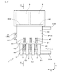
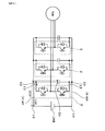
本形態の電力変換装置1は、図1〜図3に示すごとく、半導体モジュール2と、コンデンサ素子3と、正極バスバー4P及び負極バスバー4Nと、冷却部5と、を有する。
(Embodiment 1)
An embodiment relating to the power conversion device will be described with reference to FIGS. 1 to 8.
As shown in FIGS. 1 to 3, the
半導体モジュール2は、直流電源BATに電気的に接続される。コンデンサ素子3は、半導体モジュール2に電気的に接続される。正極バスバー4P及び負極バスバー4Nは、直流電源と半導体モジュール2とコンデンサ素子3とを電気的に接続する。冷却部5は、半導体モジュール2を冷却する。
The
図1、図4に示すごとく、正極バスバー4P及び負極バスバー4Nは、それぞれ、電源接続部41と、素子接続部42と、端子接続部43と、を有すると共に、第1電流経路401と、第2電流経路402と、を有する。
As shown in FIGS. 1 and 4, the positive
電源接続部41は、直流電源BATに接続される。素子接続部42は、コンデンサ素子3に接続される。端子接続部43は、半導体モジュール2のパワー端子21に接続される。図4に示すごとく、第1電流経路401は、電源接続部41と端子接続部43との間の電流経路である。第2電流経路402は、電源接続部41と素子接続部42との間の電流経路である。
The power
正極バスバー4P及び負極バスバー4Nの少なくとも一方は、いずれの第2電流経路402よりも熱抵抗が小さい第1電流経路401を有する。本形態においては、少なくとも正極バスバー4Pは、いずれの第2電流経路402よりも熱抵抗が小さい第1電流経路401を有する。すなわち、本形態においては、図4に示すごとく、正極バスバー4Pが複数の第1電流経路401を有するが、その第1電流経路401のうちでも同図の左端の端子接続部43と電源接続部41との間の第1電流経路401は、いずれの第2電流経路402よりも、熱抵抗が小さくなっている。また、それ故に、当該第1電流経路401は、いずれの第2電流経路402よりも電気抵抗も小さくなっている。
At least one of the positive
なお、正極バスバー4P及び負極バスバー4Nにおいて、熱抵抗の大小は、電気抵抗の大小と、実質的に同義となる。それゆえ、熱抵抗が大きいというときは、電気抵抗も大きいことを示し、熱抵抗が小さいというときは、電気抵抗も小さいことを示す。
また、正極バスバー4P及び負極バスバー4Nにおける電流経路は、実際にはある程度の広がりをもっているが、その中でも電流密度の高い経路に基づいて、熱抵抗、電気抵抗等の比較を行う。
In the positive
Further, although the current paths in the positive
正極バスバー4P及び負極バスバー4Nの少なくとも一方は、いずれの第2電流経路402よりも経路長が短い第1電流経路401を有する。本形態においては、少なくとも正極バスバー4Pは、いずれの第2電流経路402よりも経路長が短い第1電流経路401を有する。すなわち、本形態においては、図4に示すごとく、正極バスバー4Pが複数の第1電流経路401を有するが、その第1電流経路401のうちでも同図の左端の端子接続部43と電源接続部41との間の第1電流経路401は、いずれの第2電流経路402よりも、経路長が短くなっている。
なお、以下において、正極バスバー4P及び負極バスバー4Nについて、共通する説明においては、これらを単にバスバー4ともいう。
At least one of the positive
In the following, in the common description of the positive
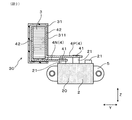
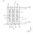
図5に示すごとく、本例の電力変換装置1は、複数の半導体モジュール2が積層配置された積層体11を有する。図1に示すごとく、積層体11に対して、積層方向Xに直交する横方向Yにずれた位置に、コンデンサ素子3が配置されている。
As shown in FIG. 5, the
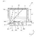
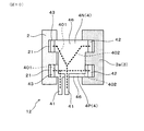
図6〜図8に示すごとく、正極バスバー4P及び負極バスバー4Nは、第1電流経路401の一部と第2電流経路402の一部とを少なくとも構成する共通部44と、共通部44から分岐して端子接続部43をそれぞれ備えた複数の分岐部45とを有する。
As shown in FIGS. 6 to 8, the positive
正極バスバー4P及び負極バスバー4Nの少なくとも一方は、共通部44における第1電流経路401を基準にして、横方向Yにおいて、端子接続部43までの距離L1が、素子接続部42までの距離L2よりも短い。
本形態においては、正極バスバー4P及び負極バスバー4Nの双方において、共通部44における第1電流経路401を基準にして、端子接続部43までの横方向Yの距離L1が、素子接続部42までの横方向Yの距離L2よりも短い。
At least one of the positive
In this embodiment, in both the positive
共通部44における第1電流経路401は、図6、図7に示すごとく、共通部44における、複数の分岐部45との境界部分付近を繋ぐような経路となる。この経路の位置が、横方向Yにおいて、素子接続部42よりも端子接続部43の方に近い。
なお、以下において、積層方向Xを適宜X方向ともいう。また、横方向Yを適宜Y方向ともいう。また、X方向とY方向との双方に直交する方向を、適宜、Z方向ともいう。なお、後述の半導体モジュール2のパワー端子21の突出方向は、Z方向となる。
As shown in FIGS. 6 and 7, the first
In the following, the stacking direction X is also appropriately referred to as the X direction. Further, the lateral direction Y is also appropriately referred to as a Y direction. Further, a direction orthogonal to both the X direction and the Y direction is also appropriately referred to as a Z direction. The protruding direction of the
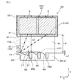
本形態において、図1、図2に示すごとく、半導体モジュール2は、IGBT(絶縁ゲートバイポーラトランジスタの略)、MOSFET(MOS型電界効果トランジスタの略)等からなるスイッチング素子を内蔵したモジュール本体部20から、複数のパワー端子21を突出してなる。本形態においては、互いに直列接続された2つのスイッチング素子を、一つの半導体モジュール2のモジュール本体部20に内蔵している。そして、半導体モジュール2は、3本のパワー端子21を突出してなる。これらのパワー端子21としては、正極バスバー4Pに接続されるものと、負極バスバー4Nに接続されるものと、図示を省略する出力バスバーに接続されるものとがある。
In this embodiment, as shown in FIGS. 1 and 2, the
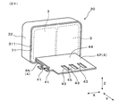
コンデンサ素子3は、図2、図6に示すごとく、コンデンサケース32内において、封止樹脂31にて封止されている。また、正極バスバー4P及び負極バスバー4Nは、素子接続部42を含む一部を、封止樹脂31にて封止されている。このようにして、コンデンサ素子3とコンデンサケース32と封止樹脂31と正極バスバー4P及び負極バスバー4Nとが一体化されて、図6、図8に示すコンデンサモジュール30が構成されている。
As shown in FIGS. 2 and 6, the
図2、図6に示すごとく、正極バスバー4P及び負極バスバー4Nの少なくとも一方は、その一部が封止樹脂31にて封止されている。そして、図6、図7に示すごとく、第1電流経路401の少なくとも一部が封止樹脂31から露出している。本形態においては、正極バスバー4P及び負極バスバー4Nのいずれもが、その一部において封止樹脂31に封止されている。そして、各バスバー4において、実質的に第1電流経路401の全体が、封止樹脂31から露出している。
As shown in FIGS. 2 and 6, at least one of the positive
図2、図6〜図8に示すごとく、封止樹脂31は、Y方向の一方にポッティング面311を向けて、コンデンサケース32から露出している。このポッティング面311から、Y方向に突出するように、正極バスバー4P及び負極バスバー4Nが延設されている。正極バスバー4P及び負極バスバー4Nは、ポッティング面311から延設した部分において、互いにZ方向に対向して配置されている。
As shown in FIGS. 2 and 6 to 8, the sealing
図2に示すごとく、この対向部分において、正極バスバー4Pと負極バスバー4Nとは、厚み方向に所定の間隔を設けて配置されている。そして、正極バスバー4Pは、負極バスバー4Nよりも、Y方向においてポッティング面311から遠い位置まで延設されている。なお、バスバー4のY方向の延設長さの関係は、特に限定されるものではなく、正極バスバー4Pよりも負極バスバー4Nが長い態様とすることもできる。
As shown in FIG. 2, in the facing portion, the positive
また、図6、図7に示すごとく、正極バスバー4P及び負極バスバー4Nは、その延設方向の端部付近に、それぞれ複数の分岐部45を有する。複数の分岐部45は、X方向に配列している。X方向に配列された分岐部45の間に、Z方向に貫通した開口部450が形成されている。この開口部450の内側端縁の一部が、端子接続部43となり、パワー端子21が接続される。
Further, as shown in FIGS. 6 and 7, the positive
開口部450のY方向における素子接続部42に最も近い位置は、素子接続部42よりも、端子接続部43に近い。つまり、開口部450のY方向における素子接続部42に最も近い位置と端子接続部43との間のY方向の距離L3が、開口部450のY方向における素子接続部42に最も近い位置と素子接続部42との間の距離L4よりも、短い。
The position of the
また、正極バスバー4P及び負極バスバー4Nにおける、封止樹脂31から露出した部分において、X方向の一端側の辺に、電源接続部41が設けてある。本形態においては、電源接続部41は、正極バスバー4P及び負極バスバー4Nから、X方向に突出している。正極バスバー4Pの電源接続部41と、負極バスバー4Nの電源接続部41とは、Z方向から見たとき、互いにY方向に並ぶように隣接配置されている。
Further, in the portions of the positive
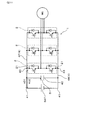
図5に示すごとく、積層体11を構成する複数の半導体モジュール2は、複数の冷却管51と共にX方向に積層されている。半導体モジュール2は、X方向の両面から冷却管51に挟持された状態となっており、両面から放熱できるよう構成されている。本形態において、半導体モジュール2を冷却する冷却部5は、複数の冷却管51を積層配置してなる冷却器からなる。冷却管51は、内部に冷媒を流通させる冷媒流路を備えている。
As shown in FIG. 5, the plurality of
冷却器は、複数の冷却管51と共に、これらを連結する複数の連結管52と、内部に冷媒を導入する冷媒導入口531と、内部から冷媒を排出する冷媒排出口532と、を有する。冷却器は、冷媒導入口531から導入された冷媒が、各冷却管51に分配されて流通するよう構成されている。これにより、冷却管51において、冷媒と半導体モジュール2とが熱交換する。これにより、半導体モジュール2において発熱した熱の一部が、冷媒へ放熱される。
The cooler has a plurality of cooling
電力変換装置1は、図3に示すごとく、直流電源BATからの直流電力を、複数の半導体モジュール2にて構成される電力変換部において交流電力に変換して、交流負荷MGへ供給することができるよう構成されている。交流負荷MGは、例えば、三相交流モーターであり、発電機としても機能する。発電機としての交流負荷MGにおいて発電された交流電力は、電力変換部において直流電力に変換され、直流電源BATに回収される。
As shown in FIG. 3, the
ここで、直流電源BATと電力変換部との間には、コンデンサ素子3が電気的に接続されている。コンデンサ素子3は、直流電源BATからの電流に含まれるリプル電流を吸収して、電力変換部へ供給される電流が、リプルが除去された直流電流となるようにしている。また、コンデンサ素子3は、電力変換部から供給された回生電流に含まれるリプルを吸収して、リプルが除去された直流電流が直流電源BATに回収されるにしている。
Here, the
コンデンサ素子3には、リプル電流をはじめとする交流電流が流れるが、直流電流は流れない。それゆえ、素子接続部42と電源接続部41との間の電流経路、すなわち、第2電流経路402には、交流電流は流れるが、直流電流は流れない。
An alternating current such as a ripple current flows through the
一方、直流電源BATと半導体モジュール2との間には、直流電流が流れる。それゆえ、端子接続部43と電源接続部41との間の電流経路、すなわち第1電流経路401には、直流電流が流れる。また、コンデンサ素子3と半導体モジュール2との間の電流経路には、交流電流が流れる。
On the other hand, a direct current flows between the direct current power supply BAT and the
そして、バスバー4において、交流電流よりも、直流電流の方が、大きい電流が流れる。それゆえ、直流電流が流れる第1電流経路401においては、この直流電流に起因するジュール熱が発生しやすい。その結果、バスバー4における、第1電流経路401及びその近傍は高温となりやすい。なお、半導体モジュール2も高温となりやすいが、冷却器にて冷却され、温度上昇を抑制することができる。
Then, in the
一方、交流電流が流れる第2電流経路402においては、特に大きな発熱は生じない。しかし、第1電流経路401において発熱した熱が、伝熱によって第2電流経路402付近の部位を通じて、コンデンサ素子3に伝わることは考えられる。それゆえ、第2電流経路402における熱抵抗が小さいと、結局、第1電流経路401からの伝熱によって、コンデンサ素子3の温度が上昇することが懸念される。そこで、本形態においては、第2電流経路402の熱抵抗を、第1電流経路401よりも大きくしている。これにより、第1電流経路401の熱がコンデンサ素子3に移動することを抑制している。
On the other hand, in the second
また、第1電流経路401の熱抵抗を小さくすることで、その電気抵抗も小さくすることができる。それゆえ、この第1電流経路401において生じるジュール熱を抑制している。その結果、第1電流経路401から第2電流経路402を介してコンデンサ素子3へ伝わる熱を、極力抑制している。図3には、正極バスバー4Pにおける、第1電流経路401の一つと第2電流経路402とに、それぞれ相当する回路上の電流経路を、破線矢印にて示している。
Further, by reducing the thermal resistance of the first
なお、本形態において、正極バスバー4Pは、電源接続部41と3つのパワー端子21との間の第1電流経路401を3つ有する。これらの3つの第1電流経路401は、互いに熱抵抗が異なるが、いずれについても、極力熱抵抗が小さいことが好ましい。
また、正極バスバー4Pは、電源接続部41と複数のコンデンサ素子3との間に、複数の第2電流経路402を有する。この複数の第2電流経路402における熱抵抗のいずれよりも、複数の第1電流経路401における熱抵抗の方が、小さいことが好ましい。さらに好ましくは、すべての第1電流経路401について、いずれの第2電流経路402よりも、熱抵抗が小さいことが好ましい。
In this embodiment, the positive
Further, the positive
また、本形態において、正極バスバー4Pは、その厚みが全体にわたって略同等である。それゆえ、第1電流経路401と第2電流経路402との関係は、その経路長についても同様である。すなわち、正極バスバー4Pは、いずれの第2電流経路402よりも経路長の短い第1電流経路401を有する。そして、複数の第1電流経路401が、いずれの第2電流経路402よりも経路長が短いことが好ましい。さらには、すべての第1電流経路401が、いずれの第2電流経路402よりも経路長が短いことが好ましい。
Further, in the present embodiment, the thickness of the positive
また、負極バスバー4Nにおいても、いずれの第2電流経路402よりも熱抵抗が小さい第1電流経路401を有することが好ましい。そして、負極バスバー4Nにおいても、複数の第2電流経路402と、複数の第1電流経路401が存在し、これらの熱抵抗、経路長についての関係も、上述の正極バスバー4Pにおけるものと同様に考えることができる。
Further, it is preferable that the negative
すなわち、負極バスバー4Nにおいても、複数の第2電流経路402における熱抵抗のいずれよりも、複数の第1電流経路401における熱抵抗の方が、小さいことが好ましい。さらに好ましくは、すべての第1電流経路401について、いずれの第2電流経路402よりも、熱抵抗が小さいことが好ましい。また、負極バスバー4Nにおいても、複数の第1電流経路401が、いずれの第2電流経路402よりも経路長が短いことがより好ましい。さらには、すべての第1電流経路401が、いずれの第2電流経路402よりも経路長が短いことが好ましい。
That is, even in the negative
次に、本実施形態の作用効果につき説明する。
上記電力変換装置1において、正極バスバー4P及び負極バスバー4Nの少なくとも一方は、いずれの第2電流経路402よりも熱抵抗が小さい第1電流経路401を有する。それゆえ、少なくとも一つの第1電流経路401は、第2電流経路402よりも熱抵抗が小さい。熱抵抗が小さいということは、電気抵抗も小さいため、当該第1電流経路401に流れる直流電流に起因する発熱量を抑制することができる。その一方で、当該第1電流経路401よりも、第2電流経路402の熱抵抗が大きいため、第1電流経路401からコンデンサ素子3への伝熱量を抑制することができる。その結果、コンデンサ素子3の温度上昇を抑制することができる。
Next, the action and effect of this embodiment will be described.
In the
また、正極バスバー4P及び負極バスバー4Nの少なくとも一方は、いずれの第2電流経路402よりも経路長が短い第1電流経路401を有する。これにより、コンデンサ素子3の温度上昇を抑制することができる電力変換装置1を容易に構成することができる。例えば、バスバー4を略均一な厚み、均質な材料にて構成する場合、経路長において、第1電流経路401を第2電流経路402よりも短くすることで、上述の効果を容易に得ることができる。
Further, at least one of the positive
正極バスバー4P及び負極バスバー4Nの少なくとも一方は、共通部44における第1電流経路401を基準にして、横方向Yにおいて、端子接続部43までの距離L1が、素子接続部42までの距離L2よりも短い。これにより、共通部44における第1電流経路401の熱が、コンデンサ素子3に伝わることを効果的に抑制することができる。その結果、コンデンサ素子3の温度上昇をより効果的に抑制することができる。
At least one of the positive
また、第1電流経路401の少なくとも一部が封止樹脂31から露出している。これにより、発熱しやすい第1電流経路401の熱が、封止樹脂31内にこもることを防ぐことができる。それゆえ、バスバー4の放熱を効率的に行うことができ、コンデンサ素子3に伝わる熱を抑制することができる。
Further, at least a part of the first
以上のごとく、本形態によれば、コンデンサ素子の温度上昇を抑制することができる電力変換装置を提供することができる。 As described above, according to the present embodiment, it is possible to provide a power conversion device capable of suppressing a temperature rise of the capacitor element.
(実施形態2)
本形態は、図9、図10に示すごとく、コンデンサ素子3が、電力変換部の各レグを構成する半導体モジュール2のそれぞれに並列接続されたレグコンデンサである、電力変換装置1の形態である。
すなわち、本形態のコンデンサ素子3は、上アームスイッチング素子と下アームスイッチング素子との直列接続体に、並列接続されている。
(Embodiment 2)
As shown in FIGS. 9 and 10, this embodiment is a form of a
That is, the
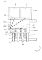
かかる構成の電力変換装置1においても、正極バスバー4Pと負極バスバー4Nのうち少なくとも一方は、いずれの第2電流経路402よりも熱抵抗が小さい第1電流経路401を有する。特に、本形態においては、正極バスバー4Pと負極バスバー4Nの双方が、いずれの第2電流経路402よりも熱抵抗が小さい第1電流経路401を有する。また、これを実現するためのバスバー4の構造、半導体モジュール2及びコンデンサモジュール3aの配置の一例が、図10に示す態様である。
Even in the
同図に示す1つの半導体モジュール2と1つのコンデンサモジュール3aと、一対のバスバー4とによって、電力変換回路における1つのレグが構成される。この構造体を、便宜的に、レグ構造体12という。
One
同図に示す態様は、各バスバー4が、半導体モジュール2の一つのパワー端子21と、コンデンサモジュール3aの端子との間に、両者を電気的に接続する連結部46を有する。そして各バスバー4は、連結部46の一部から電源接続部41を突出してなる。この電源接続部41は、連結部46における素子接続部42と端子接続部43との間の中央よりも、端子接続部43に近い位置に形成されている。これにより、電源接続部41から端子接続部43までの電流経路である第1電流経路401を、電源接続部41から素子接続部42までの電流経路である第2電流経路402よりも、経路長を短くし、その熱抵抗を小さくしている。図9には、正極バスバー4Pにおける、第1電流経路401の一つと第2電流経路402とに、それぞれ相当する回路上の電流経路を、破線矢印にて示している。
In the embodiment shown in the figure, each
なお、図10においては、1レグ分のレグ構造体12を示したが、電力変換装置1は、略同様のレグ構造体12を少なくとも3個備える。すなわち、三相交流負荷MGを駆動するための電力変換装置1は、少なくとも3層分のレグ構造体12を有する。そして、これらすべてのレグ構造体12が、上述の構成を有することが好ましい。これにより、すべての第1電流経路401が、いずれの第2電流経路402よりも、経路長が短く、また、熱抵抗が小さい、という構成が得られる。
また、各レグ構造体12における電源接続部41は、他のバスバー(図示略)を介して、直流電源BATの電極に接続された構成とすることができる。
Although the
Further, the power
なお、実施形態2以降において用いた符号のうち、既出の実施形態において用いた符号と同一のものは、特に示さない限り、既出の実施形態におけるものと同様の構成要素等を表す。 In addition, among the codes used in the second and subsequent embodiments, the same codes as those used in the above-described embodiments represent the same components and the like as those in the above-mentioned embodiments, unless otherwise specified.
本発明は上記各実施形態に限定されるものではなく、その要旨を逸脱しない範囲において種々の実施形態に適用することが可能である。 The present invention is not limited to each of the above embodiments, and can be applied to various embodiments without departing from the gist thereof.
1 電力変換装置
2 半導体モジュール
3 コンデンサ素子
4P 正極バスバー
4N 負極バスバー
401 第1電流経路
402 第2電流経路
41 電源接続部
42 素子接続部
43 端子接続部
1
Claims (4)
上記半導体モジュールに電気的に接続されるコンデンサ素子(3)と、
上記直流電源と上記半導体モジュールと上記コンデンサ素子とを電気的に接続する正極バスバー(4P)及び負極バスバー(4N)と、
上記半導体モジュールを冷却する冷却部(5)と、を有し、
上記正極バスバー及び上記負極バスバーは、それぞれ、上記直流電源に接続される電源接続部(41)と、上記コンデンサ素子に接続される素子接続部(42)と、上記半導体モジュールのパワー端子に接続される端子接続部(43)と、を有すると共に、上記電源接続部と上記端子接続部との間の電流経路である第1電流経路(401)と、上記電源接続部と上記素子接続部との間の電流経路である第2電流経路(402)と、を有し、
上記正極バスバー及び上記負極バスバーの少なくとも一方は、いずれの上記第2電流経路よりも熱抵抗が小さい上記第1電流経路を有する、電力変換装置(1)。 A semiconductor module (2) that is electrically connected to a direct current power supply (BAT),
A capacitor element (3) electrically connected to the semiconductor module and
A positive electrode bus bar (4P) and a negative electrode bus bar (4N) that electrically connect the DC power supply, the semiconductor module, and the capacitor element, and
It has a cooling unit (5) for cooling the semiconductor module.
The positive electrode bus bar and the negative electrode bus bar are connected to a power supply connection portion (41) connected to the DC power supply, an element connection portion (42) connected to the capacitor element, and a power terminal of the semiconductor module, respectively. The first current path (401), which is a current path between the power supply connection portion and the terminal connection portion, and the power supply connection portion and the element connection portion, are provided with the terminal connection portion (43). It has a second current path (402), which is a current path between the two.
The power conversion device (1), wherein at least one of the positive electrode bus bar and the negative electrode bus bar has the first current path having a thermal resistance smaller than that of any of the second current paths.
上記正極バスバー及び上記負極バスバーは、上記第1電流経路の一部と上記第2電流経路の一部とを少なくとも構成する共通部(44)と、上記共通部から分岐して上記端子接続部をそれぞれ備えた複数の分岐部(45)とを有し、
上記正極バスバー及び上記負極バスバーの少なくとも一方は、上記共通部における上記第1電流経路を基準にして、上記横方向において、上記端子接続部までの距離(L1)が、上記素子接続部までの距離(L2)よりも短い、請求項1又は2に記載の電力変換装置。 The capacitor element has a laminate (11) in which a plurality of the semiconductor modules are laminated, and the capacitor element is arranged at a position shifted in the lateral direction (Y) orthogonal to the lamination direction (X) with respect to the laminate. Has been
The positive electrode bus bar and the negative electrode bus bar have a common portion (44) that constitutes at least a part of the first current path and a part of the second current path, and a terminal connection portion branched from the common portion. Each has a plurality of branch portions (45) provided with the same.
For at least one of the positive electrode bus bar and the negative electrode bus bar, the distance (L1) to the terminal connection portion in the lateral direction is the distance to the element connection portion with reference to the first current path in the common portion. The power conversion device according to claim 1 or 2, which is shorter than (L2).
Priority Applications (6)
| Application Number | Priority Date | Filing Date | Title |
|---|---|---|---|
| JP2019086404A JP6977743B2 (en) | 2019-04-26 | 2019-04-26 | Power converter |
| CN202080031107.6A CN113728546B (en) | 2019-04-26 | 2020-04-09 | power conversion device |
| DE112020002123.8T DE112020002123T5 (en) | 2019-04-26 | 2020-04-09 | power converter |
| PCT/JP2020/015974 WO2020218014A1 (en) | 2019-04-26 | 2020-04-09 | Power conversion device |
| US16/857,036 US20200340229A1 (en) | 2019-04-26 | 2020-04-23 | Toilet bowl |
| US17/508,589 US12136892B2 (en) | 2019-04-26 | 2021-10-22 | Power converter for suppressing heat transfer to electrical component |
Applications Claiming Priority (1)
| Application Number | Priority Date | Filing Date | Title |
|---|---|---|---|
| JP2019086404A JP6977743B2 (en) | 2019-04-26 | 2019-04-26 | Power converter |
Publications (2)
| Publication Number | Publication Date |
|---|---|
| JP2020184810A true JP2020184810A (en) | 2020-11-12 |
| JP6977743B2 JP6977743B2 (en) | 2021-12-08 |
Family
ID=72916715
Family Applications (1)
| Application Number | Title | Priority Date | Filing Date |
|---|---|---|---|
| JP2019086404A Active JP6977743B2 (en) | 2019-04-26 | 2019-04-26 | Power converter |
Country Status (5)
| Country | Link |
|---|---|
| US (2) | US20200340229A1 (en) |
| JP (1) | JP6977743B2 (en) |
| CN (1) | CN113728546B (en) |
| DE (1) | DE112020002123T5 (en) |
| WO (1) | WO2020218014A1 (en) |
Cited By (3)
| Publication number | Priority date | Publication date | Assignee | Title |
|---|---|---|---|---|
| WO2022235052A1 (en) * | 2021-05-03 | 2022-11-10 | 주식회사 엘지에너지솔루션 | Battery module and battery pack including same |
| JP2023177397A (en) * | 2022-06-02 | 2023-12-14 | 三菱電機株式会社 | power converter |
| JP2024063269A (en) * | 2022-10-26 | 2024-05-13 | 三菱電機株式会社 | Power Conversion Equipment |
Families Citing this family (3)
| Publication number | Priority date | Publication date | Assignee | Title |
|---|---|---|---|---|
| US12003184B2 (en) * | 2019-06-24 | 2024-06-04 | Volvo Construction Equipment Ab | Power converter assembly and a power system |
| DE102022207478A1 (en) * | 2022-07-21 | 2024-02-01 | Zf Friedrichshafen Ag | Modular intermediate circuit capacitor and power converter with such an intermediate circuit capacitor |
| DE102023105341A1 (en) * | 2023-03-03 | 2024-09-05 | Seg Automotive Germany Gmbh | Half-bridge switch arrangement |
Citations (5)
| Publication number | Priority date | Publication date | Assignee | Title |
|---|---|---|---|---|
| JP2012249480A (en) * | 2011-05-31 | 2012-12-13 | Hitachi Automotive Systems Ltd | Electric power conversion apparatus |
| JP2014064407A (en) * | 2012-09-21 | 2014-04-10 | Denso Corp | Power conversion device |
| JP2018067998A (en) * | 2016-10-18 | 2018-04-26 | 三菱電機株式会社 | Power converter |
| JP2019017246A (en) * | 2018-09-06 | 2019-01-31 | 株式会社デンソー | Power conversion device |
| JP2019030043A (en) * | 2017-07-25 | 2019-02-21 | 株式会社デンソー | Power converter |
Family Cites Families (12)
| Publication number | Priority date | Publication date | Assignee | Title |
|---|---|---|---|---|
| JP5289348B2 (en) * | 2010-01-22 | 2013-09-11 | 三菱電機株式会社 | Automotive power converter |
| JP5422466B2 (en) * | 2010-04-01 | 2014-02-19 | 日立オートモティブシステムズ株式会社 | Power converter |
| JP5403089B2 (en) * | 2011-05-26 | 2014-01-29 | 株式会社デンソー | Power converter |
| JP5505398B2 (en) * | 2011-11-11 | 2014-05-28 | 株式会社デンソー | Power converter |
| JP5888185B2 (en) | 2012-08-24 | 2016-03-16 | 株式会社デンソー | Capacitor device |
| JP5655846B2 (en) * | 2012-12-04 | 2015-01-21 | 株式会社デンソー | Power converter |
| WO2015145679A1 (en) * | 2014-03-27 | 2015-10-01 | 株式会社日立製作所 | Power conversion unit, power conversion apparatus, and power conversion apparatus manufacturing method |
| JP6349275B2 (en) * | 2015-03-05 | 2018-06-27 | 日立オートモティブシステムズ株式会社 | Power converter |
| US9584061B1 (en) * | 2015-09-17 | 2017-02-28 | Toyota Motor Engineering & Manufacturing North America, Inc. | Electric drive systems including smoothing capacitor cooling devices and systems |
| JP6361646B2 (en) * | 2015-12-25 | 2018-07-25 | 株式会社デンソー | Power converter |
| JP6919348B2 (en) * | 2017-06-07 | 2021-08-18 | 株式会社デンソー | Power converter |
| JP6877694B2 (en) | 2017-11-07 | 2021-05-26 | トヨタ自動車株式会社 | Navigation devices, navigation methods, and navigation programs |
-
2019
- 2019-04-26 JP JP2019086404A patent/JP6977743B2/en active Active
-
2020
- 2020-04-09 CN CN202080031107.6A patent/CN113728546B/en active Active
- 2020-04-09 DE DE112020002123.8T patent/DE112020002123T5/en active Pending
- 2020-04-09 WO PCT/JP2020/015974 patent/WO2020218014A1/en not_active Ceased
- 2020-04-23 US US16/857,036 patent/US20200340229A1/en not_active Abandoned
-
2021
- 2021-10-22 US US17/508,589 patent/US12136892B2/en active Active
Patent Citations (5)
| Publication number | Priority date | Publication date | Assignee | Title |
|---|---|---|---|---|
| JP2012249480A (en) * | 2011-05-31 | 2012-12-13 | Hitachi Automotive Systems Ltd | Electric power conversion apparatus |
| JP2014064407A (en) * | 2012-09-21 | 2014-04-10 | Denso Corp | Power conversion device |
| JP2018067998A (en) * | 2016-10-18 | 2018-04-26 | 三菱電機株式会社 | Power converter |
| JP2019030043A (en) * | 2017-07-25 | 2019-02-21 | 株式会社デンソー | Power converter |
| JP2019017246A (en) * | 2018-09-06 | 2019-01-31 | 株式会社デンソー | Power conversion device |
Cited By (4)
| Publication number | Priority date | Publication date | Assignee | Title |
|---|---|---|---|---|
| WO2022235052A1 (en) * | 2021-05-03 | 2022-11-10 | 주식회사 엘지에너지솔루션 | Battery module and battery pack including same |
| JP2023177397A (en) * | 2022-06-02 | 2023-12-14 | 三菱電機株式会社 | power converter |
| JP7809017B2 (en) | 2022-06-02 | 2026-01-30 | 三菱電機株式会社 | Power Conversion Device |
| JP2024063269A (en) * | 2022-10-26 | 2024-05-13 | 三菱電機株式会社 | Power Conversion Equipment |
Also Published As
| Publication number | Publication date |
|---|---|
| DE112020002123T5 (en) | 2022-01-27 |
| US12136892B2 (en) | 2024-11-05 |
| US20200340229A1 (en) | 2020-10-29 |
| CN113728546B (en) | 2024-01-05 |
| CN113728546A (en) | 2021-11-30 |
| WO2020218014A1 (en) | 2020-10-29 |
| JP6977743B2 (en) | 2021-12-08 |
| US20220045626A1 (en) | 2022-02-10 |
Similar Documents
| Publication | Publication Date | Title |
|---|---|---|
| JP6977743B2 (en) | Power converter | |
| JP4920677B2 (en) | Power conversion device and assembly method thereof | |
| KR101522089B1 (en) | Semiconductor unit | |
| CN102612747B (en) | Semiconductor module | |
| JP5488638B2 (en) | Power converter | |
| CN101681898B (en) | Cooling structure for semiconductor elements | |
| CN103081326B (en) | Inverter unit | |
| JP6429721B2 (en) | Power converter and railway vehicle | |
| CN111480231B (en) | power conversion device | |
| CN113678246B (en) | Semiconductor device with a semiconductor device having a plurality of semiconductor chips | |
| JP6690478B2 (en) | Power converter | |
| JP2010153527A (en) | Device for cooling semiconductor module | |
| JP7711821B2 (en) | Power Conversion Equipment | |
| JP6908061B2 (en) | Power converter | |
| CN113557603B (en) | Semiconductor devices | |
| JP2019122064A (en) | Power conversion device | |
| JP4356434B2 (en) | 3-level inverter circuit | |
| JP5169092B2 (en) | Power converter | |
| JP6973313B2 (en) | Power converter | |
| JPWO2019043886A1 (en) | Power converter | |
| JP2014096412A (en) | Semiconductor module | |
| JP6973269B2 (en) | Power converter | |
| JP7003641B2 (en) | Semiconductor modules and power converters | |
| JP6680393B2 (en) | Power converter | |
| JP2024101333A (en) | Power Conversion Equipment |
Legal Events
| Date | Code | Title | Description |
|---|---|---|---|
| A621 | Written request for application examination |
Free format text: JAPANESE INTERMEDIATE CODE: A621 Effective date: 20210225 |
|
| TRDD | Decision of grant or rejection written | ||
| A01 | Written decision to grant a patent or to grant a registration (utility model) |
Free format text: JAPANESE INTERMEDIATE CODE: A01 Effective date: 20211012 |
|
| A61 | First payment of annual fees (during grant procedure) |
Free format text: JAPANESE INTERMEDIATE CODE: A61 Effective date: 20211025 |
|
| R151 | Written notification of patent or utility model registration |
Ref document number: 6977743 Country of ref document: JP Free format text: JAPANESE INTERMEDIATE CODE: R151 |
|
| R250 | Receipt of annual fees |
Free format text: JAPANESE INTERMEDIATE CODE: R250 |
|
| R250 | Receipt of annual fees |
Free format text: JAPANESE INTERMEDIATE CODE: R250 |