JP2020177458A - Capacitive panel sensor - Google Patents
Capacitive panel sensor Download PDFInfo
- Publication number
- JP2020177458A JP2020177458A JP2019079372A JP2019079372A JP2020177458A JP 2020177458 A JP2020177458 A JP 2020177458A JP 2019079372 A JP2019079372 A JP 2019079372A JP 2019079372 A JP2019079372 A JP 2019079372A JP 2020177458 A JP2020177458 A JP 2020177458A
- Authority
- JP
- Japan
- Prior art keywords
- signal
- electrode line
- capacitance
- panel sensor
- capacitance type
- Prior art date
- Legal status (The legal status is an assumption and is not a legal conclusion. Google has not performed a legal analysis and makes no representation as to the accuracy of the status listed.)
- Pending
Links
Images

Landscapes
- Geophysics And Detection Of Objects (AREA)
Description
本発明は、A/D変換入力のダイナミックレンジの制限によって検出信号の増幅率が制限され、かつ、検出対象物の有りと無しとの検出信号の差が小さい場合であっても精度良く検出対象物を検出することができる静電容量型パネルセンサに関する。 In the present invention, the amplification factor of the detection signal is limited by the limitation of the dynamic range of the A / D conversion input, and the detection target is accurately detected even when the difference between the detection signal with and without the detection target is small. It relates to a capacitance type panel sensor capable of detecting an object.
静電容量型タッチパネルは、入出力デバイスに多用されている。静電容量型タッチパネルは、センサ表面にガラスやアクリルなどの厚く硬い加飾パネルを用いることができるという利点がある。静電容量型タッチパネルは、縦横にパターニングされた透明電極を組み合わせ、センサーパネルの表面に指を近づけると、近づけた部分の電極に容量変化が生じ、この容量変化を検出することで指の位置を特定する。 Capacitive touch panels are often used in input / output devices. The capacitance type touch panel has an advantage that a thick and hard decorative panel such as glass or acrylic can be used on the sensor surface. Capacitive touch panels combine transparent electrodes that are patterned vertically and horizontally, and when a finger is brought close to the surface of the sensor panel, a capacitance change occurs in the electrode in the close area, and the position of the finger is determined by detecting this capacitance change. Identify.
ところで、静電容量型タッチパネルは、ショーケースの商品棚や倉庫棚の上面に配置し、この静電容量型タッチパネルの上面に載置される商品などの検出対象物を検出する静電容量型パネルセンサとして利用することができる。しかし、検出対象物の有無による静電容量変化は、10%程度である。このため、検出感度を上げようとする場合、アンプによって検出信号を増幅することが考えられる。しかし、検出信号はA/D変換されるため、増幅された検出信号の振幅がA/D変換入力のダイナミックレンジを超えてしまい、検出対象物の有無を検出できなくなってしまう場合があった。 By the way, the capacitance type touch panel is arranged on the upper surface of the product shelf or the warehouse shelf of the showcase, and the capacitance type panel detects an object to be detected such as a product placed on the upper surface of the capacitance type touch panel. It can be used as a sensor. However, the change in capacitance depending on the presence or absence of the object to be detected is about 10%. Therefore, when trying to increase the detection sensitivity, it is conceivable to amplify the detection signal by an amplifier. However, since the detection signal is A / D converted, the amplitude of the amplified detection signal may exceed the dynamic range of the A / D conversion input, and the presence or absence of the detection target may not be detected.
特に、検出対象物の誘電率が低い場合、検出対象物が有りのときと、無いときとの検出信号の差が小さく、検出信号を増幅しようとしてもダイナミックレンジの制限によって検出対象物の有無を精度良く検出できない場合があった。 In particular, when the permittivity of the detection target is low, the difference between the detection signal with and without the detection target is small, and even if the detection signal is to be amplified, the presence or absence of the detection target is determined by limiting the dynamic range. In some cases, it could not be detected accurately.
本発明は、上記に鑑みてなされたものであって、A/D変換入力のダイナミックレンジの制限によって検出信号の増幅率が制限され、かつ、検出対象物の有りと無しとの検出信号の差が小さい場合であっても精度良く検出対象物を検出することができる静電容量型パネルセンサを提供することを目的とする。 The present invention has been made in view of the above, and the amplification factor of the detection signal is limited by the limitation of the dynamic range of the A / D conversion input, and the difference between the detection signal with and without the detection target. It is an object of the present invention to provide a capacitance type panel sensor capable of accurately detecting an object to be detected even when the size is small.
上述した課題を解決し、目的を達成するために、本発明にかかる静電容量型パネルセンサは、送信電極線群パターンの送信電極線と受信電極線群パターンの受信電極線とが直交し電極シートの表裏に離隔配置され、前記送信電極線と前記受信電極線との交差点をマトリクス状に形成したセンサ基板上に検出対象物が載置された場合における各交差点の静電容量変化を検出する静電容量型パネルセンサであって、前記送信電極線に入力される送信信号を用いて、前記送信信号と同位相であって、前記検出対象物が載置されていない場合の前記交差点の静電容量と同等の静電容量を介して流れる電流波形を有した基準信号を生成する基準信号生成部と、前記受信電極線からの受信信号と前記基準信号との差分を増幅した信号を検出信号として出力する差動アンプと、を備えたことを特徴とする。 In order to solve the above-mentioned problems and achieve the object, in the capacitance type panel sensor according to the present invention, the transmitting electrode line of the transmitting electrode line group pattern and the receiving electrode line of the receiving electrode line group pattern are orthogonal to each other. Detects changes in capacitance at each intersection when a detection object is placed on a sensor substrate that is separated from the front and back of the sheet and has a matrix of intersections between the transmission electrode line and the reception electrode line. It is a capacitance type panel sensor, and uses the transmission signal input to the transmission electrode line, is in phase with the transmission signal, and is static at the intersection when the detection object is not placed. A reference signal generator that generates a reference signal having a current waveform flowing through a capacitance equivalent to the electric capacitance, and a detection signal that amplifies the difference between the received signal from the receiving electrode line and the reference signal. It is characterized by being equipped with a differential amplifier that outputs as.
また、本発明にかかる静電容量型パネルセンサは、上記の発明において、前記基準信号生成部は、前記検出対象物が載置された場合の静電容量変化が小さくなるに従って、前記基準信号のレベルを、前記検出対象物が載置されていない場合の受信信号のレベルに近づけることを特徴とする。 Further, in the capacitance type panel sensor according to the present invention, in the above invention, the reference signal generation unit of the reference signal becomes smaller as the change in capacitance when the detection object is placed becomes smaller. It is characterized in that the level is brought close to the level of the received signal when the detection object is not placed.
また、本発明にかかる静電容量型パネルセンサは、上記の発明において、前記基準信号生成部は、前記交差点の静電容量と同等の静電容量を有し、前記送信信号が入力されるコンデンサと、前記コンデンサから出力される信号レベルに対してゲイン調整した信号を前記基準信号として前記差動アンプに出力するゲイン調整アンプと、を備えたことを特徴とする。 Further, in the capacitance type panel sensor according to the present invention, in the above invention, the reference signal generation unit has a capacitance equivalent to the capacitance at the intersection, and the capacitor to which the transmission signal is input. It is characterized by including a gain adjusting amplifier for outputting a signal whose gain is adjusted with respect to a signal level output from the capacitor as a reference signal to the differential amplifier.
また、本発明にかかる静電容量型パネルセンサは、上記の発明において、前記コンデンサは、前記送信電極線群パターンの各送信電極線の入力側にそれぞれ接続される複数のコンデンサであることを特徴とする。 Further, the capacitance type panel sensor according to the present invention is characterized in that, in the above invention, the capacitor is a plurality of capacitors connected to the input side of each transmission electrode line of the transmission electrode line group pattern. And.
また、本発明にかかる静電容量型パネルセンサは、上記の発明において、前記コンデンサは、前記送信電極線群パターンの各送信電極線の入力側にそれぞれ静電結合する配線パターン間の容量であることを特徴とする。 Further, in the capacitance type panel sensor according to the present invention, in the above invention, the capacitor is a capacitance between wiring patterns that are electrostatically coupled to the input side of each transmission electrode line of the transmission electrode line group pattern. It is characterized by that.
また、本発明にかかる静電容量型パネルセンサは、上記の発明において、前記配線パターンは、前記送信電極線群パターンと前記受信電極線群パターンとを表裏に形成する電極シートの前記受信電極線群パターン側に形成されることを特徴とする。 Further, in the capacitance type panel sensor according to the present invention, in the above invention, the wiring pattern is the receiving electrode wire of the electrode sheet forming the transmitting electrode wire group pattern and the receiving electrode wire group pattern on the front and back surfaces. It is characterized in that it is formed on the group pattern side.
また、本発明にかかる静電容量型パネルセンサは、上記の発明において、複数の異なる静電容量を有し、前記送信信号が入力される複数のコンデンサと、前記複数のコンデンサのうちのいずれか一つを選択し、選択されたコンデンサを介した信号を前記基準信号として前記差動アンプに出力する選択スイッチと、を備えたことを特徴とする。 Further, in the above invention, the capacitance type panel sensor according to the present invention has a plurality of different capacitances, and is one of a plurality of capacitors into which the transmission signal is input and the plurality of capacitors. It is characterized by including a selection switch for selecting one and outputting a signal through the selected capacitor to the differential amplifier as the reference signal.
また、本発明にかかる静電容量型パネルセンサは、上記の発明において、前記検出対象物は商品棚上に陳列される商品であり、前記センサ基板は前記商品棚上に配置されることを特徴とする。 Further, the capacitance type panel sensor according to the present invention is characterized in that, in the above invention, the detection target is a product displayed on a product shelf, and the sensor substrate is arranged on the product shelf. And.
本発明によれば、A/D変換入力のダイナミックレンジの制限によって検出信号の増幅率が制限され、かつ、検出対象物が有りと無しとの検出信号の差が小さい場合であっても精度良く検出対象物を検出することができる。 According to the present invention, the amplification factor of the detection signal is limited by the limitation of the dynamic range of the A / D conversion input, and the difference between the detection signal with and without the detection target is small, with high accuracy. The object to be detected can be detected.
以下、添付図面を参照してこの発明を実施するための形態について説明する。 Hereinafter, embodiments for carrying out the present invention will be described with reference to the accompanying drawings.
<全体構成>
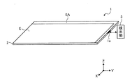
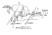
図1は、本発明の実施の形態である静電容量型パネルセンサ1の全体構成を示す斜視図である。また、図2は、図1に示した静電容量型パネルセンサ1の断面構成を示す図である。なお、静電容量型パネルセンサ1は、表面側(+Z方向)に載置された検出対象物の有無を静電容量の変化によって検出するセンサである。例えば、ショーケースの商品棚に載置された缶飲料、ペットボトル、煙草、薬などを商品の有無を検出する。図1に示すように、静電容量型パネルセンサ1は、検出対象物が載置される検出領域Eとマトリクス駆動部EAとを有するセンサ基板2である。
<Overall configuration>
FIG. 1 is a perspective view showing the overall configuration of the capacitance type panel sensor 1 according to the embodiment of the present invention. Further, FIG. 2 is a diagram showing a cross-sectional configuration of the capacitance type panel sensor 1 shown in FIG. The capacitance type panel sensor 1 is a sensor that detects the presence or absence of a detection object mounted on the surface side (+ Z direction) by changing the capacitance. For example, the presence or absence of products is detected for canned beverages, PET bottles, cigarettes, medicines, etc. placed on the product shelves of showcases. As shown in FIG. 1, the capacitance type panel sensor 1 is a
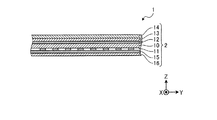
図2に示すように、センサ基板2は、電極シートであるPETフィルム10の裏面(−Z方向)に複数の送信電極線11からなる送信電極線パターンが描かれ、表面に複数の受信電極線12からなる受信電極線パターンが描かれている。複数の送信電極線11は、X方向に延びて所定のピッチで平行配置される。複数の受信電極線12は、Y方向に延びて所定のピッチで平行配置される。複数の送信電極線11と複数の受信電極線12とは、PETフィルム10の厚みの間隔で離隔配置され、Z方向からみた、複数の送信電極線11と複数の受信電極線12との交差点がマトリクス状に配置される。静電容量型パネルセンサ1は、各交差点での静電容量変化を検出し、2次元の静電容量変化画像を生成することによって、上部に載置された検出対象物の有無を検出することができる。
As shown in FIG. 2, in the
受信電極線パターンの表面側及び送信電極線パターンの裏面側には、それぞれ両面テープ13,15を介してそれぞれ保護膜としてのPETフィルム14,16が積層される。
なお、センサ基板2は、コネクタ1aを介して検出部3に接続される。検出部3は、送信信号を送信電極線11に出力し、受信電極線12から出力される検出信号を受信して検出対象物の有無を検出する。
The
<検出動作>
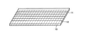
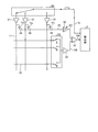
次に、静電容量型パネルセンサ1の動作について説明する。図3に示すように、静電容量型パネルセンサ1は、PETフィルム10を挟んで複数の送信電極線11及び複数の受信電極線12が直交して配置される。
<Detection operation>
Next, the operation of the capacitance type panel sensor 1 will be described. As shown in FIG. 3, in the capacitance type panel sensor 1, a plurality of
図4に示すように、複数の送信電極線11及び複数の受信電極線12が直交する交差点は、PETフィルム10の厚みの間隔で離隔されているため、結合容量Ceが発生している。この状態で、検出部3は、送信電極線11に30Vの矩形波信号Siを印加すると、受信電極線12から各交差点に対応する検出信号SBが出力される。
As shown in FIG. 4, the intersections where the plurality of transmitting
検出部3から入力された送信信号である矩形波信号Siは、セレクタ20を介して各送信電極線11に出力される。この際、矩形波信号Siは、アンプ21によって増幅される。各受信電極線12からは、各送信電極線11との各交差点で発生した検出信号をセレクタ22を介して出力され、その後、アンプ23によって増幅された検出信号SBを差動アンプ31の+端に出力する。
The rectangular wave signal Si, which is a transmission signal input from the detection unit 3, is output to each
一方、ゲイン調整アンプ30には、送信線11aに接続される静電容量Ccを有するコンデンサ33を介した送信信号Siを増幅し、この増幅した校正信号SCを基準信号として差動アンプ31の−端に出力する。なお、校正信号SCは、静電容量型パネルセンサ1の表面に検出対象物が載置されていない状態における検出信号SB0を模擬する信号であり、ゲイン調整アンプ30は、コンデンサ33を介して入力される送信信号Siのゲインが調整されている。
On the other hand, the
差動アンプ31は、検出信号SBから校正信号SCを減算した差分を増幅した検出信号SAとして検出部3に出力する。
The
コンデンサ33、ゲイン調整アンプ30は、基準信号生成部として機能し、この基準信号生成部及び差動アンプ31を設けない場合、検出信号SBがそのまま検出部3に出力される。ここで、検出対象物が載置された状態の検出信号SBを検出信号SB1とし、検出対象物が載置されない状態の検出信号SBを検出信号SB0とすると、検出部3は、検出信号SB0と検出信号SB1との差ΔSBをもとに、検出対象物の載置有無を検出する。ここで、検出対象物が煙草などの誘電率が低いものである場合、静電容量変化は小さく、この差ΔSBが極めて小さくなる。そこで、アンプ23のゲインを大きくし、あるいは高段にアンプを設けてゲインを大きくした場合、検出部3のA/D変換入力のダイナミックレンジを超えてしまい、検出対象物の有無を検出することができない。
The
そこで、本実施の形態では、基準信号生成部及び差動アンプ31を設けて校正信号SCを生成し、差動アンプ31が検出信号SBから校正信号SCを差し引いた信号を増幅した検出信号SAを検出部3に出力している。校正信号SCは、検出信号SB0に近い値である。検出信号SA0は、検出信号SB0から校正信号SCを差し引いて増幅した信号であり、検出信号SA1は、検出信号SB1から校正信号SCを差し引いて増幅した信号である。この検出信号SA0と検出信号SA1との差ΔSAは、A/D変換入力のダイナミックレンジ内に十分収まる値となり、しかも差ΔSBを拡大した値である。これにより、検出対象物が煙草などの誘電率が低いものであって静電容量変化が小さい場合であっても、A/D変換入力のダイナミックレンジ内で検出感度を向上させることができる。
Therefore, in the present embodiment, the reference signal generator and the
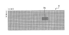
図5は、検出信号SAの値をもとに生成した底面形状画像Dの一例を示す図である。この底面形状画像Dは、XY平面の2次元画像である。図5では、静電容量型パネルセンサ1上に煙草を載置した場合の底面形状画像Dを示している。底面形状画像D内にペットボトルの底面に対応する2次元位置に画像Daが現れている。検出部3は、この底面形状画像Dを利用する図示しない外部装置に出力する。 FIG. 5 is a diagram showing an example of a bottom surface shape image D generated based on the value of the detection signal SA. This bottom shape image D is a two-dimensional image of the XY plane. FIG. 5 shows a bottom surface shape image D when a cigarette is placed on the capacitance type panel sensor 1. Image Da appears at a two-dimensional position corresponding to the bottom surface of the PET bottle in the bottom shape image D. The detection unit 3 outputs the bottom surface shape image D to an external device (not shown) that uses the bottom shape image D.
<検出動作の詳細>
図6は、図4に示した交差点であるA部の送信電極線11と受信電極線12との間で生成する電気力線の状態及び電流の流れを示す図である。まず、検出部3から送信された矩形波信号Siは、入力電流iとして送信電極線11を流れる。入力電流iは、受信電極線12の交差点では結合容量Ceを介した変位電流分である出力電流i0が受信電極線12に流れる。ここで、送信電極線11と受信電極線12との間の電気力線は、静電容量型パネルセンサ1の上部に検出対象物100が載置されている場合、検出対象物100側への電気力線が増大し、検出対象物100に対して微小な変位電流分が漏れ電流i1として流れる。この結果、受信電極線12を流れる出力電流は、出力電流i0から漏れ電流i1分、差し引いた出力電流(i0−i1)となる。この差は上記の差ΔSBである。
<Details of detection operation>
FIG. 6 is a diagram showing a state of electric lines of force generated between a transmitting
一方、送信線11aには、コンデンサ33が接続され、このコンデンサ33を介した変位電流(校正電流)分が出力電流i0´としてゲイン調整アンプ30側に流れる。この結果、差動アンプ31は、検出対象物100が載置されていないときの検出電流SA0は、出力電流i0から出力電流i0´を減算して所定ゲインG分、増幅した値となる。また、検出対象物100が載置されているときの検出電流SA1は、出力電流i0から、漏れ電流i1及び出力電流i0´を減算して所定ゲインG分、増幅した値となる。ここで、出力電流i0と出力電流i0´の値が近い値であると、検出電流SA0は、ほぼ0になり、検出電流SA1は、(−i1)となり、検出対象物100に流れた漏れ電流i1のみを検出できることになる。
On the other hand, a
なお、ゲイン調整アンプ30のゲインは、静電容量型パネルセンサ1に載置される検出対象物100の誘電率や形状などによって予め設定しておくことができる。検出対象物100の誘電率が低く、差ΔSBが小さい場合には、出力電流i0と出力電流i0´との値が近くなるようにゲイン調整しておき、検出対象物100の誘電率が高く、差ΔSBが大きい場合には、出力電流i0´の値が出力電流i0よりも小さくなるようにゲイン調整しておけばよい。すなわち、差ΔSAがA/D変換入力のダイナミックレンジ内に収まり、かつ、大きな値となるようにゲイン調整する。
The gain of the
<変形例1>
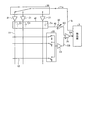
図7は、変形例1による静電容量型パネルセンサの構成を示す回路図である。上述した実施の形態では、送信線11aにコンデンサ33を直接接続し、送信線11aから矩形波信号Siを直接取得するようにしていたが、本変形例1では、アンプ21の後段であって、検出領域E外に、送信電極線11に直交する校正電極線40を設けるとともに、各送信電極線11と校正電極線40との間にそれぞれコンデンサ34を設け、校正電極線40を介して矩形波信号Siを得るようにしている。なお、コンデンサ34は、静電容量Ccである。また、校正電極線40は、受信電極線12に対して平行配置されることになる。
<Modification example 1>
FIG. 7 is a circuit diagram showing the configuration of the capacitance type panel sensor according to the first modification. In the above-described embodiment, the
<変形例2>
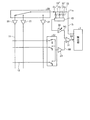
図8は、変形例2による静電容量型パネルセンサの構成を示す回路図である。変形例1では、校正電極線40と送信電極線11との間にコンデンサ34を設けるようにしていたが、本変形例2では、校正電極線40に替えてベタな配線パターンである平板校正電極線41を設け、送信電極線11と平板校正電極線41との間をそれぞれ静電結合し、それぞれ静電容量Ccが生成できるようにしている。
<
FIG. 8 is a circuit diagram showing a configuration of a capacitance type panel sensor according to the second modification. In the first modification, the
なお、配線パターンである平板校正電極線41は、送信電極線群パターンと受信電極線群パターンとを表裏に形成するPETフィルム10の受信電極線群パターン側に形成される。なお、平板校正電極線41は、校正電極線40と同様に、アンプ21の後段であって、検出領域E外に設けられる。
The flat plate
<変形例3>
図9は、変形例3による静電容量型パネルセンサの構成を示す回路図である。上述した実施の形態及び変形例1,2では、静電容量型パネルセンサ1に載置される検出対象物に応じてゲイン調整アンプ30のゲインを調整していたが、本変形例2では、複数の異なるコンデンサ33,33´,33´´を送信線11aに予め接続しておき、静電容量型パネルセンサ1に載置される検出対象物に応じたコンデンサ33,33´,33´´をセレクタ43によって選択し、選択したコンデンサ33,33´,33´´を経由した矩形波信号Siをゲイン調整アンプ30に入力するようにしている。この場合、ゲイン調整アンプ30は調整せず、セレクタ43の選択設定のみでよい。
<Modification example 3>
FIG. 9 is a circuit diagram showing the configuration of the capacitance type panel sensor according to the modified example 3. In the above-described embodiments and
なお、本実施の形態及び変形例で示した静電容量型パネルセンサ1は、ショーケースの商品棚や倉庫棚以外にも適用することができる。たとえば、ベルトコンベアなどの搬送路上に静電容量型パネルセンサ1を設けることによって、搬送される物品の形状や材料を検出することができる。 The capacitance type panel sensor 1 shown in the present embodiment and the modified example can be applied to other than the product shelf and the warehouse shelf of the showcase. For example, by providing the capacitance type panel sensor 1 on a transport path such as a belt conveyor, the shape and material of the transported article can be detected.
また、上記の実施の形態及び変形例で図示した各構成は機能概略的なものであり、必ずしも物理的に図示の構成をされていることを要しない。すなわち、各装置及び構成要素の分散・統合の形態は図示のものに限られず、その全部又は一部を各種の使用状況などに応じて、任意の単位で機能的又は物理的に分散・統合して構成することができる。 In addition, each configuration shown in the above-described embodiment and modification is a schematic function, and does not necessarily have to be physically shown. That is, the form of distribution / integration of each device and component is not limited to the one shown in the figure, and all or part of the device and components are functionally or physically distributed / integrated in arbitrary units according to various usage conditions. Can be configured.
1 静電容量型パネルセンサ
1a コネクタ
2 センサ基板
3 検出部
10,14,16 PETフィルム
11 送信電極線
11a 送信線
12 受信電極線
13,15 両面テープ
20,22,43 セレクタ
21,23 アンプ
30 ゲイン調整アンプ
31 差動アンプ
33,33´,33´´,34 コンデンサ
40 校正電極線
41 平板校正電極線
100 検出対象物
Cc 静電容量
Ce 結合容量
D 底面形状画像
Da 画像
E 検出領域
EA マトリクス駆動部
G 所定ゲイン
i 入力電流
i0,i0´ 出力電流
i1 漏れ電流
SA,SA0,SA1,SB,SB0,SB1 検出信号
SC 校正信号
Si 矩形波信号
ΔSA,ΔSB 差
1 Capacitance type panel
Claims (8)
前記送信電極線に入力される送信信号を用いて、前記送信信号と同位相であって、前記検出対象物が載置されていない場合の前記交差点の静電容量と同等の静電容量を介して流れる電流波形を有した基準信号を生成する基準信号生成部と、
前記受信電極線からの受信信号と前記基準信号との差分を増幅した信号を検出信号として出力する差動アンプと、
を備えたことを特徴とする静電容量型パネルセンサ。 The transmitting electrode line of the transmitting electrode line group pattern and the receiving electrode line of the receiving electrode line group pattern are orthogonal to each other and are separated from each other on the front and back surfaces of the electrode sheet, and the intersections of the transmitting electrode line and the receiving electrode line are formed in a matrix. A capacitance type panel sensor that detects changes in capacitance at each intersection when an object to be detected is placed on the sensor substrate.
Using the transmission signal input to the transmission electrode line, the capacitance is in phase with the transmission signal and is equivalent to the capacitance at the intersection when the detection object is not placed. A reference signal generator that generates a reference signal with a current waveform that flows through
A differential amplifier that outputs a signal obtained by amplifying the difference between the received signal from the receiving electrode line and the reference signal as a detection signal, and
Capacitive panel sensor characterized by being equipped with.
前記交差点の静電容量と同等の静電容量を有し、前記送信信号が入力されるコンデンサと、
前記コンデンサから出力される信号レベルに対してゲイン調整した信号を前記基準信号として前記差動アンプに出力するゲイン調整アンプと、
を備えたことを特徴とする請求項1又は2に記載の静電容量型パネルセンサ。 The reference signal generator
A capacitor having a capacitance equivalent to that of the intersection and to which the transmission signal is input,
A gain adjusting amplifier that outputs a gain-adjusted signal with respect to the signal level output from the capacitor as the reference signal to the differential amplifier, and
The capacitance type panel sensor according to claim 1 or 2, further comprising.
前記複数のコンデンサのうちのいずれか一つを選択し、選択されたコンデンサを介した信号を前記基準信号として前記差動アンプに出力する選択スイッチと、
を備えたことを特徴とする請求項1又は2に記載の静電容量型パネルセンサ。 A plurality of capacitors having a plurality of different capacitances to which the transmission signal is input, and
A selection switch that selects any one of the plurality of capacitors and outputs a signal via the selected capacitor to the differential amplifier as the reference signal.
The capacitance type panel sensor according to claim 1 or 2, further comprising.
Priority Applications (1)
| Application Number | Priority Date | Filing Date | Title |
|---|---|---|---|
| JP2019079372A JP2020177458A (en) | 2019-04-18 | 2019-04-18 | Capacitive panel sensor |
Applications Claiming Priority (1)
| Application Number | Priority Date | Filing Date | Title |
|---|---|---|---|
| JP2019079372A JP2020177458A (en) | 2019-04-18 | 2019-04-18 | Capacitive panel sensor |
Publications (1)
| Publication Number | Publication Date |
|---|---|
| JP2020177458A true JP2020177458A (en) | 2020-10-29 |
Family
ID=72936669
Family Applications (1)
| Application Number | Title | Priority Date | Filing Date |
|---|---|---|---|
| JP2019079372A Pending JP2020177458A (en) | 2019-04-18 | 2019-04-18 | Capacitive panel sensor |
Country Status (1)
| Country | Link |
|---|---|
| JP (1) | JP2020177458A (en) |
-
2019
- 2019-04-18 JP JP2019079372A patent/JP2020177458A/en active Pending
Similar Documents
| Publication | Publication Date | Title |
|---|---|---|
| US10852873B2 (en) | Pressure-sensitive detection apparatus, electronic device, and touch display screen | |
| US9348470B2 (en) | Projected capacitance touch panel with reference and guard electrode | |
| US8841927B2 (en) | Touch sensing circuit | |
| US8937607B2 (en) | Capacitive touch panel with dynamically allocated electrodes | |
| CN103294295B (en) | Mutual inductance type capacitive touch screen | |
| EP2750001B1 (en) | Touch panel and touch detecting method therefor | |
| US20110102353A1 (en) | Touch panel apparatus and a method for detecting a contact position on the same | |
| JP2019517001A (en) | Film thickness detector | |
| JP6845590B2 (en) | Transparent touch screen parametric emitter | |
| US10001884B2 (en) | Voltage driven self-capacitance measurement | |
| JP2007533220A5 (en) | ||
| JP2020177458A (en) | Capacitive panel sensor | |
| JP2009094849A (en) | Capacitance change detection circuit, touch panel, and determination method | |
| TWI514225B (en) | Capacitive touch panel module | |
| JP2019522792A (en) | Film thickness detection apparatus and method | |
| KR20140045378A (en) | Capacitive sensor and method for detecting a number of objects | |
| CN106462282A (en) | Cantilevered displacement sensors and methods of determining touching forces on touch screen | |
| JP2020177477A (en) | Capacitive panel sensor | |
| TW201706814A (en) | Touch detection method and capacitive sensing device | |
| KR102786037B1 (en) | Electrostatic capacity detection device and electrostatic capacity detection method | |
| JP2009026767A (en) | Static capacitance sensor component, object mounting body, semiconductor manufacturing device, and liquid crystal display element manufacturing device | |
| KR102644978B1 (en) | Display device, system and method for mutual capacitance sensing | |
| US20230221150A1 (en) | Capacitance detection device | |
| JP2020009358A (en) | Capacitive panel sensor | |
| KR101645668B1 (en) | Capacitance measuring circuit and touch input device including the same |