JP2020150168A - Semiconductor device and manufacturing method thereof - Google Patents
Semiconductor device and manufacturing method thereof Download PDFInfo
- Publication number
- JP2020150168A JP2020150168A JP2019047449A JP2019047449A JP2020150168A JP 2020150168 A JP2020150168 A JP 2020150168A JP 2019047449 A JP2019047449 A JP 2019047449A JP 2019047449 A JP2019047449 A JP 2019047449A JP 2020150168 A JP2020150168 A JP 2020150168A
- Authority
- JP
- Japan
- Prior art keywords
- reflectance
- semiconductor substrate
- layer
- region
- film
- Prior art date
- Legal status (The legal status is an assumption and is not a legal conclusion. Google has not performed a legal analysis and makes no representation as to the accuracy of the status listed.)
- Pending
Links
Images


Classifications
-
- H—ELECTRICITY
- H01—ELECTRIC ELEMENTS
- H01L—SEMICONDUCTOR DEVICES NOT COVERED BY CLASS H10
- H01L23/00—Details of semiconductor or other solid state devices
- H01L23/564—Details not otherwise provided for, e.g. protection against moisture
-
- B—PERFORMING OPERATIONS; TRANSPORTING
- B23—MACHINE TOOLS; METAL-WORKING NOT OTHERWISE PROVIDED FOR
- B23K—SOLDERING OR UNSOLDERING; WELDING; CLADDING OR PLATING BY SOLDERING OR WELDING; CUTTING BY APPLYING HEAT LOCALLY, e.g. FLAME CUTTING; WORKING BY LASER BEAM
- B23K26/00—Working by laser beam, e.g. welding, cutting or boring
- B23K26/36—Removing material
- B23K26/38—Removing material by boring or cutting
-
- H—ELECTRICITY
- H01—ELECTRIC ELEMENTS
- H01L—SEMICONDUCTOR DEVICES NOT COVERED BY CLASS H10
- H01L21/00—Processes or apparatus adapted for the manufacture or treatment of semiconductor or solid state devices or of parts thereof
- H01L21/02—Manufacture or treatment of semiconductor devices or of parts thereof
- H01L21/04—Manufacture or treatment of semiconductor devices or of parts thereof the devices having at least one potential-jump barrier or surface barrier, e.g. PN junction, depletion layer or carrier concentration layer
- H01L21/18—Manufacture or treatment of semiconductor devices or of parts thereof the devices having at least one potential-jump barrier or surface barrier, e.g. PN junction, depletion layer or carrier concentration layer the devices having semiconductor bodies comprising elements of Group IV of the Periodic System or AIIIBV compounds with or without impurities, e.g. doping materials
- H01L21/26—Bombardment with radiation
- H01L21/263—Bombardment with radiation with high-energy radiation
- H01L21/268—Bombardment with radiation with high-energy radiation using electromagnetic radiation, e.g. laser radiation
-
- H—ELECTRICITY
- H01—ELECTRIC ELEMENTS
- H01L—SEMICONDUCTOR DEVICES NOT COVERED BY CLASS H10
- H01L21/00—Processes or apparatus adapted for the manufacture or treatment of semiconductor or solid state devices or of parts thereof
- H01L21/02—Manufacture or treatment of semiconductor devices or of parts thereof
- H01L21/04—Manufacture or treatment of semiconductor devices or of parts thereof the devices having at least one potential-jump barrier or surface barrier, e.g. PN junction, depletion layer or carrier concentration layer
- H01L21/18—Manufacture or treatment of semiconductor devices or of parts thereof the devices having at least one potential-jump barrier or surface barrier, e.g. PN junction, depletion layer or carrier concentration layer the devices having semiconductor bodies comprising elements of Group IV of the Periodic System or AIIIBV compounds with or without impurities, e.g. doping materials
- H01L21/30—Treatment of semiconductor bodies using processes or apparatus not provided for in groups H01L21/20 - H01L21/26
- H01L21/302—Treatment of semiconductor bodies using processes or apparatus not provided for in groups H01L21/20 - H01L21/26 to change their surface-physical characteristics or shape, e.g. etching, polishing, cutting
- H01L21/304—Mechanical treatment, e.g. grinding, polishing, cutting
-
- H—ELECTRICITY
- H01—ELECTRIC ELEMENTS
- H01L—SEMICONDUCTOR DEVICES NOT COVERED BY CLASS H10
- H01L21/00—Processes or apparatus adapted for the manufacture or treatment of semiconductor or solid state devices or of parts thereof
- H01L21/02—Manufacture or treatment of semiconductor devices or of parts thereof
- H01L21/04—Manufacture or treatment of semiconductor devices or of parts thereof the devices having at least one potential-jump barrier or surface barrier, e.g. PN junction, depletion layer or carrier concentration layer
- H01L21/50—Assembly of semiconductor devices using processes or apparatus not provided for in a single one of the subgroups H01L21/06 - H01L21/326, e.g. sealing of a cap to a base of a container
- H01L21/56—Encapsulations, e.g. encapsulation layers, coatings
-
- H—ELECTRICITY
- H01—ELECTRIC ELEMENTS
- H01L—SEMICONDUCTOR DEVICES NOT COVERED BY CLASS H10
- H01L21/00—Processes or apparatus adapted for the manufacture or treatment of semiconductor or solid state devices or of parts thereof
- H01L21/67—Apparatus specially adapted for handling semiconductor or electric solid state devices during manufacture or treatment thereof; Apparatus specially adapted for handling wafers during manufacture or treatment of semiconductor or electric solid state devices or components ; Apparatus not specifically provided for elsewhere
- H01L21/683—Apparatus specially adapted for handling semiconductor or electric solid state devices during manufacture or treatment thereof; Apparatus specially adapted for handling wafers during manufacture or treatment of semiconductor or electric solid state devices or components ; Apparatus not specifically provided for elsewhere for supporting or gripping
- H01L21/6835—Apparatus specially adapted for handling semiconductor or electric solid state devices during manufacture or treatment thereof; Apparatus specially adapted for handling wafers during manufacture or treatment of semiconductor or electric solid state devices or components ; Apparatus not specifically provided for elsewhere for supporting or gripping using temporarily an auxiliary support
- H01L21/6836—Wafer tapes, e.g. grinding or dicing support tapes
-
- H—ELECTRICITY
- H01—ELECTRIC ELEMENTS
- H01L—SEMICONDUCTOR DEVICES NOT COVERED BY CLASS H10
- H01L21/00—Processes or apparatus adapted for the manufacture or treatment of semiconductor or solid state devices or of parts thereof
- H01L21/70—Manufacture or treatment of devices consisting of a plurality of solid state components formed in or on a common substrate or of parts thereof; Manufacture of integrated circuit devices or of parts thereof
- H01L21/77—Manufacture or treatment of devices consisting of a plurality of solid state components or integrated circuits formed in, or on, a common substrate
- H01L21/78—Manufacture or treatment of devices consisting of a plurality of solid state components or integrated circuits formed in, or on, a common substrate with subsequent division of the substrate into plural individual devices
-
- H—ELECTRICITY
- H01—ELECTRIC ELEMENTS
- H01L—SEMICONDUCTOR DEVICES NOT COVERED BY CLASS H10
- H01L23/00—Details of semiconductor or other solid state devices
- H01L23/28—Encapsulations, e.g. encapsulating layers, coatings, e.g. for protection
- H01L23/31—Encapsulations, e.g. encapsulating layers, coatings, e.g. for protection characterised by the arrangement or shape
- H01L23/3157—Partial encapsulation or coating
- H01L23/3171—Partial encapsulation or coating the coating being directly applied to the semiconductor body, e.g. passivation layer
-
- H—ELECTRICITY
- H01—ELECTRIC ELEMENTS
- H01L—SEMICONDUCTOR DEVICES NOT COVERED BY CLASS H10
- H01L23/00—Details of semiconductor or other solid state devices
- H01L23/28—Encapsulations, e.g. encapsulating layers, coatings, e.g. for protection
- H01L23/31—Encapsulations, e.g. encapsulating layers, coatings, e.g. for protection characterised by the arrangement or shape
- H01L23/3157—Partial encapsulation or coating
- H01L23/3192—Multilayer coating
-
- H—ELECTRICITY
- H01—ELECTRIC ELEMENTS
- H01L—SEMICONDUCTOR DEVICES NOT COVERED BY CLASS H10
- H01L2221/00—Processes or apparatus adapted for the manufacture or treatment of semiconductor or solid state devices or of parts thereof covered by H01L21/00
- H01L2221/67—Apparatus for handling semiconductor or electric solid state devices during manufacture or treatment thereof; Apparatus for handling wafers during manufacture or treatment of semiconductor or electric solid state devices or components; Apparatus not specifically provided for elsewhere
- H01L2221/683—Apparatus for handling semiconductor or electric solid state devices during manufacture or treatment thereof; Apparatus for handling wafers during manufacture or treatment of semiconductor or electric solid state devices or components; Apparatus not specifically provided for elsewhere for supporting or gripping
- H01L2221/68304—Apparatus for handling semiconductor or electric solid state devices during manufacture or treatment thereof; Apparatus for handling wafers during manufacture or treatment of semiconductor or electric solid state devices or components; Apparatus not specifically provided for elsewhere for supporting or gripping using temporarily an auxiliary support
- H01L2221/68327—Apparatus for handling semiconductor or electric solid state devices during manufacture or treatment thereof; Apparatus for handling wafers during manufacture or treatment of semiconductor or electric solid state devices or components; Apparatus not specifically provided for elsewhere for supporting or gripping using temporarily an auxiliary support used during dicing or grinding
-
- H—ELECTRICITY
- H01—ELECTRIC ELEMENTS
- H01L—SEMICONDUCTOR DEVICES NOT COVERED BY CLASS H10
- H01L2221/00—Processes or apparatus adapted for the manufacture or treatment of semiconductor or solid state devices or of parts thereof covered by H01L21/00
- H01L2221/67—Apparatus for handling semiconductor or electric solid state devices during manufacture or treatment thereof; Apparatus for handling wafers during manufacture or treatment of semiconductor or electric solid state devices or components; Apparatus not specifically provided for elsewhere
- H01L2221/683—Apparatus for handling semiconductor or electric solid state devices during manufacture or treatment thereof; Apparatus for handling wafers during manufacture or treatment of semiconductor or electric solid state devices or components; Apparatus not specifically provided for elsewhere for supporting or gripping
- H01L2221/68304—Apparatus for handling semiconductor or electric solid state devices during manufacture or treatment thereof; Apparatus for handling wafers during manufacture or treatment of semiconductor or electric solid state devices or components; Apparatus not specifically provided for elsewhere for supporting or gripping using temporarily an auxiliary support
- H01L2221/6834—Apparatus for handling semiconductor or electric solid state devices during manufacture or treatment thereof; Apparatus for handling wafers during manufacture or treatment of semiconductor or electric solid state devices or components; Apparatus not specifically provided for elsewhere for supporting or gripping using temporarily an auxiliary support used to protect an active side of a device or wafer
Abstract
Description
本発明の実施形態は、半導体装置および半導体装置の製造方法に関する。 Embodiments of the present invention relate to semiconductor devices and methods for manufacturing semiconductor devices.
デバイス層が形成された半導体基板のダイシング領域に沿って、半導体基板の内部にレーザ光を集光することによって改質層を形成し、劈開させて複数のチップに個片化するステルスダイシング技術が知られている。 A stealth dicing technology that forms a modified layer by condensing laser light inside the semiconductor substrate along the dicing region of the semiconductor substrate on which the device layer is formed, and cleaves it into pieces into multiple chips. Are known.
しかしながら、半導体基板の厚さが薄くなると、ステルスダイシング技術を用いて半導体基板をダイシングすることが困難となる。 However, when the thickness of the semiconductor substrate becomes thin, it becomes difficult to dice the semiconductor substrate by using the stealth dicing technique.
本発明の一つの実施形態は、半導体基板の厚さが薄くても、ステルスダイシング技術を用いて、半導体基板をダイシングすることができる半導体装置および半導体装置の製造方法を提供することを目的とする。 One embodiment of the present invention aims to provide a semiconductor device and a method for manufacturing a semiconductor device capable of dicing a semiconductor substrate by using a stealth dicing technique even if the thickness of the semiconductor substrate is thin. ..
本発明の一つの実施形態によれば、半導体装置は、デバイス層と、反射率低減層と、改質層と、を備える。前記デバイス層は、半導体基板の第1領域の第1面上に配置される。前記反射率低減層は、前記半導体基板の前記第1領域の周囲に設けられる第2領域の前記第1面上に配置され、前記第1面上に金属膜が配置された場合の前記第1面に対向する第2面側から入射されるレーザ光の反射率に比して反射率を低減する。前記改質層は、前記第2領域の前記半導体基板の側面に設けられる。前記第2領域の前記半導体基板の側面は、前記半導体基板の中を伸展した切断面である。 According to one embodiment of the present invention, the semiconductor device includes a device layer, a reflectance reducing layer, and a modified layer. The device layer is arranged on the first surface of the first region of the semiconductor substrate. The reflectance reducing layer is arranged on the first surface of a second region provided around the first region of the semiconductor substrate, and the first surface when a metal film is arranged on the first surface. The reflectance is reduced as compared with the reflectance of the laser beam incident from the second surface side facing the surface. The modified layer is provided on the side surface of the semiconductor substrate in the second region. The side surface of the semiconductor substrate in the second region is a cut surface extended in the semiconductor substrate.
以下に添付図面を参照して、実施形態にかかる半導体装置および半導体装置の製造方法を詳細に説明する。なお、これらの実施形態により本発明が限定されるものではない。また、以下の実施形態で用いられる半導体装置の断面図は模式的なものであり、層の厚みと幅との関係や各層の厚みの比率などは現実のものとは異なる場合がある。 The semiconductor device according to the embodiment and the method for manufacturing the semiconductor device will be described in detail with reference to the accompanying drawings. The present invention is not limited to these embodiments. Further, the cross-sectional view of the semiconductor device used in the following embodiments is schematic, and the relationship between the thickness and width of the layers, the ratio of the thickness of each layer, and the like may differ from the actual ones.
(第1の実施形態)
まず、ステルスダイシングについて説明する。図1は、ステルスダイシングを用いた半導体装置の製造方法の手順の一例を示すフローチャートである。図2−1〜図2−2は、ステルスダイシングを用いた半導体装置の製造法の手順の一例を模式的に示す断面図である。なお、図2−1で、デバイスウェハ11の厚さ方向をZ方向とし、Z方向に垂直な方向でかつステルスダイシング時のレーザの走査方向をY方向とし、Z方向およびY方向に垂直な方向をX方向とする。
(First Embodiment)
First, stealth dicing will be described. FIG. 1 is a flowchart showing an example of a procedure of a method for manufacturing a semiconductor device using stealth dicing. 2-1 to 2-2 are cross-sectional views schematically showing an example of a procedure of a method for manufacturing a semiconductor device using stealth dicing. In FIG. 2-1 the thickness direction of the
まず、加工対象の半導体装置10が用意される。半導体装置10は、半導体基板であるデバイスウェハ11の第1面11a側にデバイス層12が設けられたものである。デバイスウェハ11は、例えばシリコンウェハである。デバイス層12は、電界効果型トランジスタなどの素子と、素子間を接続する配線層と、を含む。例えばNAND型フラッシュメモリを構成するメモリセルを含む層でもよい。また、この半導体装置10のデバイス層12上には、パッシベーション膜21が設けられる。パッシベーション膜21は、例えば、第1領域であるデバイス配置領域Rdvを覆うように形成される。この例では、パッシベーション膜21は、デバイス配置領域Rdvの周囲に配置される第2領域であるダイシング領域Rdには設けられていない。ダイシング領域Rdは、デバイスウェハ11の劈開しやすい結晶方位に沿って設けられる。例えばシリコンウェハの(100)基板の場合には、ダイシング領域Rdは<111>方向に沿って設けられる。
First, the
この半導体装置10のパッシベーション膜21およびデバイス層12上に、図示しない接着剤によってテープ22を貼り付ける(ステップS11、図2−1(a)))。ここで、テープ22は、例えば、表面保護テープである。テープ22は、例えば、基材および粘着剤を含む。
A
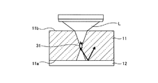
ついで、デバイスウェハ11が所定の厚さとなるように、デバイスウェハ11の第1面11aに対向する第2面11bから、例えば研削砥石で研削する(ステップS12、図2−1(b))。その後、デバイスウェハ11の第2面11b側からレーザ光Lを照射し、レーザ光Lをデバイスウェハ11の内部で集光して改質層31を形成する(ステップS13、図2−2(c))。レーザ光Lは、例えば、赤外領域の透過レーザである。レーザ光Lは、例えばY方向に沿って走査される。
Then, the
レーザ光Lがデバイスウェハ11に照射されると、レーザ光Lが集光された集光点30では、シリコンが瞬間的に気化し、ボイド32が形成される。また、気化するときの引っ張り応力と、冷えたときにボイド32が形成されるときの圧縮応力と、によってデバイスウェハ11中に亀裂33が形成される。改質層31は、ボイド32と亀裂33とを含む。
When the
ダイシング領域Rdに沿って、改質層31を形成した後、図示しない接着剤によってテープ23を貼り付けることで、デバイスウェハ11を固定する(ステップS14)。ここで、接着剤は、例えば、DAF(Die Attach Film)である。テープ23は、例えば、基材および粘着剤を含む。そして、テープ23を外周に向かって全体を引っ張る(ステップS15、図2−2(d))。これによって、個々のボイド32に伴って形成される亀裂33が、デバイスウェハ11からデバイス層12の表面まで延び、チップ100に個片化される。なお、この例では、改質層31を形成した後でテープ23を貼り付けているが、改質層31を形成する前に貼り付けてもよい。以上によって、半導体装置が製造される。
After forming the modified
ところで、デバイスウェハ11の厚さが例えば30μmよりも薄くなると、このような方法でデバイスウェハ11を個片化することが困難となる。図3は、ステルスダイシング装置における焦点位置の設定値と実際の焦点深さとの関係の一例を示す図である。この図で、横軸は、ステルスダイシング装置に設定されるデフォーカス値を示している。具体的には、ステルスダイシングを行うデバイスウェハ11でのレーザ光Lの入射面(第2面11b)から、どの深さに焦点を結ばせるかを設定する設定値である。右側に行くほど、第1面11aに近くなることを示している。縦軸は、ステルスダイシング装置によってステルスダイシングを実施したときの焦点深さである。改質層31のボイド32の最も第1面11a側に近い部分が集光点30となり、この位置が実際の焦点深さとなる。
By the way, if the thickness of the
この図に示されるように、デフォーカス値が−4.0〜−6.5μmの範囲では、すなわちウェハ11の厚さの中心付近が焦点になる場合には、デフォーカス値である設定値に対して実際の焦点深さは直線的に変化する。つまり、集光点30は、設定した位置に形成されることになる。しかし、デフォーカス値が−6.5μmよりも小さくなると、すなわちデバイスウェハ11のデバイス層12側に近い領域が焦点になる場合には、デフォーカス値よりも実際の焦点深さの方が約6μmだけ第1面11a側に移動してしまう。つまり、集光点30は、設定した位置に形成されなくなってしまう。その結果、デバイスウェハ11を切断面である劈開面の蛇行等がない良好なダイシングがしにくくなる。
As shown in this figure, when the defocus value is in the range of -4.0 to -6.5 μm, that is, when the focus is near the center of the thickness of the
図4は、ウェハの構造による改質層の出来栄えの一例を示す図である。ここでは、表面に半導体素子が形成されたデバイスウェハ11および鏡面研磨ウェハ41の2種類のウェハについて、ステルスダイシングを行う。デバイスウェハ11および鏡面研磨ウェハ41はシリコンウェハであり、その厚さは、同一であるものとする。
FIG. 4 is a diagram showing an example of the finished product of the modified layer due to the structure of the wafer. Here, stealth dicing is performed on two types of wafers, a
デバイスウェハ11は、第1面11a側には、例えばタングステン等の金属膜を含むデバイス層12が配置され、レーザ光Lの入射面である第2面11bには半導体装置の製造工程で製造された酸化膜16が配置されている。鏡面研磨ウェハ41は、第1面41aおよび第2面41bに自然酸化膜以外の膜が配置されていないウェハである。
In the
それぞれのウェハをステルスダイシングすると、改質層31の厚さは、デバイスウェハ11の方が、鏡面研磨ウェハ41よりも少し厚い。デバイスウェハ11では、改質層31の亀裂33は、複雑な形状を有するものとなる。その結果、デバイスウェハ11を劈開面の蛇行等がない良好なダイシングがしにくくなる。一方、鏡面研磨ウェハ41では、改質層31の亀裂33は、鏡面研磨ウェハ41の厚さ方向に伸長したきれいな形を有するものとなる。
When each wafer is stealth-diced, the thickness of the modified
図4の改質層31の模式図を見ると、デバイスウェハ11の改質層に比して、鏡面研磨ウェハ41の改質層は厚さ方向に伸長したきれいな亀裂を有し、鏡面研磨ウェハ41はダイシングによってきれいな劈開面を有して劈開される。このとき、劈開面は所定の結晶方位に沿っている場合もあるが、必ずしも結晶方位に沿っていなくともよい。
Looking at the schematic view of the modified
このように、デバイスウェハ11と、鏡面研磨ウェハ41と、で違いが生じる原因として、デバイスウェハ11の第1面11a側の状態が考えられる。すなわち、デバイスウェハ11では、第1面11a側に金属膜が配置されているが、鏡面研磨ウェハ41では、第1面41a側に金属膜はなく自然酸化膜が配置されている。第1面41aに酸化シリコン膜が配置された鏡面研磨ウェハ41の第2面41b側から1,342nmの光を入射したときの反射率をシミュレーションによって計算すると17%となった。第1面11aにタングステン等の金属膜が配置されたデバイスウェハ11の第2面11b側から1,342nmの光を入射したときの反射率は、酸化シリコン膜が配置された場合よりも大きい反射率であると考えられる。
As described above, a state on the
以上のことから、第1面11aに配置された金属膜などの反射率を上昇させる膜の有無がステルスダイシングに影響を与えているものと考えらえる。図5は、金属膜の存在によるステルスダイシングへの影響を説明する図である。図5に示されるように、第1面11aにデバイス層12が配置された、厚さの薄いデバイスウェハ11では、デバイス層12中の第1面11a側に配置される金属膜によって、ステルスダイシングで使用されるレーザ光Lが反射されてしまう。図3の結果から考えると、第2面11bから所望の深さの位置に焦点を結ぼうとしても、金属膜によるレーザ光Lの反射によって、改質層31を形成する改質反応が阻害され、所望の位置に焦点を結ぶことができなくなる。あるいは、図4の結果から考えると、所望の位置に改質層を形成できたとしても、金属膜によるレーザ光Lの反射によって、鏡面研磨ウェハ41のように厚さ方向に伸長したきれいな亀裂になりにくい。これらのため、デバイスウェハ11が薄くなるにつれて、ステルスダイシングによる劈開が困難になるものと考えられる。
From the above, it can be considered that the presence or absence of a film that increases the reflectance, such as a metal film arranged on the
そこで、第1の実施形態では、デバイスウェハ11の第1面11aに金属膜を直接配置した場合に比して、レーザ光Lに対する反射率を低減した反射率低減層がウェハ11の第1面11aのダイシング領域Rd上に設けられる。
Therefore, in the first embodiment, the reflectance reducing layer having reduced reflectance with respect to the laser beam L is the first surface of the
図6は、第1の実施形態による半導体装置の構成の一例を模式的に示す斜視図である。図7は、第1の実施形態による半導体装置の構成の一例を模式的に示す図であり、(a)は第1面側から見た上面図であり、(b)は(a)の側面図である。 FIG. 6 is a perspective view schematically showing an example of the configuration of the semiconductor device according to the first embodiment. 7A and 7B are views schematically showing an example of the configuration of the semiconductor device according to the first embodiment, FIG. 7A is a top view seen from the first surface side, and FIG. 7B is a side surface of FIG. 7A. It is a figure.
図6および図7に示される半導体装置は、デバイスウェハ11からステルスダイシングによって個片化されたチップ100である。チップ100は、デバイスウェハ11の一部である矩形状の半導体基板111を有する。半導体基板111は、デバイス層12が配置される矩形状のデバイス配置領域Rdvと、デバイス配置領域Rdvの外周に沿って設けられるダイシング領域Rdと、を有する。ダイシング領域Rdは、矩形環状を有する。半導体基板111の各辺の延在方向は、劈開しやすい結晶方位に一致している。
The semiconductor device shown in FIGS. 6 and 7 is a
デバイス配置領域Rdvでは、半導体基板111の第1面11a上に金属膜を含むデバイス層12が配置される。
In the device arrangement region Rdv, the
ダイシング領域Rdでは、半導体基板111の第1面11aとデバイス層12を構成する金属膜との間に、反射率低減層13が設けられる。反射率低減層13は、第1面11aに酸化シリコン膜が配置されたシリコンウェハの第2面11b側からレーザ光Lを照射したときの反射率と同等かそれ以下となる構成を有する。ダイシング領域Rdでは、反射率低減層13の上に、デバイス配置領域Rdvに設けられる金属膜が配置される。反射率低減層13は、ダイシング領域Rdだけではなく、デバイス配置領域Rdvに設けられていてもよい。
In the dicing region Rd, a
このように、ダイシング領域Rdに反射率低減層13を設けることで、ステルスダイシング時に第2面11bから入射されるレーザ光Lのデバイスウェハ11の第1面11a側での反射が抑制される。その結果、ステルスダイシング装置で設定したデフォーカス値に対応するデバイスウェハ11内の位置に焦点を結ばせることができる。また、デバイスウェハ11の厚さ方向に伸長するきれいな亀裂33を有する改質層31を形成することができる。この改質層31によって、所定の方位を有する劈開面が形成される。
By providing the
ステルスダイシングでは、機械的にダイシングする場合に比して、取り代がない。そのため、チップ100には、上記したようにダイシング領域Rdの一部が残ることになる。半導体基板111の側面は、ダイシング領域Rdを含み、また改質層31を含む。改質層31のボイド32の最も第1面11a側に位置する部分、すなわち集光点30が、第1面11aから6μmの範囲に収めることが可能となる。ステルスダイシングでは、パルスレーザを用いて改質層31を形成する。改質層31の間隔は、パルスレーザの発振間隔と、パルスレーザと半導体装置10の間の相対的な走査速度と、に応じて変化する。
Stealth dicing has no allowance compared to mechanical dicing. Therefore, a part of the dicing region Rd remains on the
第1の実施形態では、デバイスウェハ11の第1面11aのダイシング領域Rdでデバイスウェハ11と金属膜との間に、反射率低減層13を設けた。これによって、デバイスウェハ11をステルスダイシングする場合に、デバイスウェハ11の第1面11aの界面でのレーザ光Lの反射が抑制され、デバイスウェハ11内の所望の位置に改質層31を形成することができる。その結果、約30μm以下に薄くされ、第1面11aに金属膜を含むデバイス層12が配置されたデバイスウェハ11であっても、ステルスダイシングを用いて、劈開面の蛇行等がなく良好に個片化することができる。特にデバイスウェハがさらに薄く25μm以下であっても良好に個片化することができる。
In the first embodiment, the
また、デバイス配置領域Rdvとダイシング領域Rdとを有する半導体装置10のダイシング領域Rdの半導体基板111の第1面11aとデバイス層12を構成する金属膜と同じ金属膜との間に、反射率低減層13を設けた。これによって、膜を配置した応力で半導体装置が反り上がってしまう場合に、半導体装置の反りを矯正することができる。
Further, the reflectance is reduced between the
(第2の実施形態)
第2の実施形態では、レーザ光を散乱させる反射率低減層を有する半導体装置について説明する。
(Second Embodiment)
In the second embodiment, a semiconductor device having a reflectance reducing layer that scatters laser light will be described.
図8は、ウェハの裏面仕上げの違いによる裏面の粗さと反射率の違いを示す図である。ここでは、裏面仕上げとして、メッシュサイズが#320、#4800および#8000の砥粒を用いて研磨した場合と、Gettering Dry Polish(以下、GDPという)で研磨した場合と、を例に挙げている。裏面の粗さとして、最大高さRmaxDを用いている。この図に示されるように、研磨方法が細かくなるにしたがって、粗さも小さくなり、反射率も高くなる傾向にある。 FIG. 8 is a diagram showing the difference in back surface roughness and reflectance due to the difference in back surface finish of the wafer. Here, as the back surface finishing, a case where the mesh size is polished with # 320, # 4800 and # 8000 abrasive grains and a case where the mesh size is polished with Gettering Dry Polish (hereinafter referred to as GDP) are given as an example. .. The maximum height RmaxD is used as the roughness of the back surface. As shown in this figure, as the polishing method becomes finer, the roughness tends to decrease and the reflectance tends to increase.
図9は、図8から求めた表面粗さと反射率の下降率との関係の一例を示す図である。この図で、横軸は最大高さRmaxDを示し、縦軸は反射率の下降率(%)を示している。反射率の下降率は、最も粗さが小さいGDPの裏面反射率を基準としたものである。この図に示されるように、反射率の下落率は、デバイスウェハ11の表面粗さが減少すると線形的に減少する。なお、このばあい、裏面は、レーザ光の入射面に対向する面であり、例えば第1面11aである。
FIG. 9 is a diagram showing an example of the relationship between the surface roughness obtained from FIG. 8 and the rate of decrease in reflectance. In this figure, the horizontal axis represents the maximum height RmaxD, and the vertical axis represents the rate of decrease in reflectance (%). The rate of decrease in reflectance is based on the backside reflectance of GDP, which has the smallest roughness. As shown in this figure, the rate of decrease in reflectance linearly decreases as the surface roughness of the
図4で、第1面11aに自然酸化膜が配置されている場合の反射率は17%である。金属膜を有するデバイスウェハ11の反射率を低下することができれば、ステルスダイシング時に、改質反応を阻害させずに、所望の位置に改質層31を形成することが可能になる。例えば、デバイスウェハ11のデバイス層12に金属膜を有している場合は、金属膜の材質等により異なるが、その反射率は30〜50%程度である。そのため、反射率を半減させると、反射率は15〜25%となり、良好な改質層を形成しやすくなると考えられる。そこで、図9から例えば反射率を50%低下させるためには、最大高さの目標を1.4μmとすればよいことがわかる。第1面11aに金属膜ではなく、他の種類の膜が配置された場合は、反射率などに応じて適宜、最大高さの目標値を変更する。
In FIG. 4, the reflectance is 17% when the natural oxide film is arranged on the
図10は、第2の実施形態による半導体装置の構成の一例を模式的に示す側面図である。図10は、第1の実施形態の図7(b)と同様に、個片化された半導体装置であるチップ100のダイシング領域Rdを示している。第2の実施形態のチップでは、反射率低減層13は、1.4μm以上の最大高さRmaxDを有する。この反射率低減層13の上に、金属膜を含むデバイス層12が配置される。
FIG. 10 is a side view schematically showing an example of the configuration of the semiconductor device according to the second embodiment. FIG. 10 shows the dicing region Rd of the
このような反射率低減層13は、デバイスウェハ11上に反射率低減層13を形成し、さらにその上にレジストを塗布する。その後、露光技術および現像技術を用いて、デバイス配置領域Rdvを覆い、ダイシング領域Rd上に、1.4μm以上の最大高さを形成することができるレジストパターンを形成する。そして、レジストパターンをマスクとしてRIE(Reactive Ion Etching)法などのエッチング技術を用いて加工することによって、1.4μm以上の最大高さを有する反射率低減層13が形成される。
In such a
第2の実施形態では、デバイスウェハ11のダイシング領域Rd上にRmaxDが1.4μm以上の表面粗さを有する反射率低減層13を設けた。これによって、第1の実施形態と同様に、ステルスダイシング時に、デバイスウェハ11とデバイス層12との界面でのレーザ光Lの反射を抑え、薄いデバイスウェハ11でもデバイスウェハ11内の所望の深さに改質層31を形成することができる。その結果、薄いデバイスウェハ11でも、ステルスダイシングによって、チップ100に個片化することができる。
In the second embodiment, the
(第3の実施形態)
第3の実施形態では、薄膜光学によりレーザ光の反射率を低減させる反射率低減層を有する半導体装置について説明する。
(Third Embodiment)
In the third embodiment, a semiconductor device having a reflectance reducing layer that reduces the reflectance of laser light by thin film optics will be described.
第3の実施形態では、反射率低減層13は、散乱ではなく、例えば光の干渉によって入射したレーザ光Lの反射率を抑制する材料を含む。反射率低減層13は、光学的に計算して、反射率が所定値よりも低くなる材料からなる膜を含む。反射率低減層13として、異なる誘電率を有する膜を積層した多層膜を用いることができる。反射率低減層13は、例えば、異なる誘電率を有する誘電体膜を複数積層した誘電体多層膜とすることができる。また、誘電体多層膜ではなくても、酸化膜と半導体膜とを積層させた多層膜としてもよい。
In the third embodiment, the
図11は、第3の実施形態による半導体装置の構成の一例を模式的に示す断面図である。図11は、第1の実施形態の図7(b)と同様に、個片化された半導体装置であるチップ100のダイシング領域Rdを示している。半導体基板111のデバイス配置領域Rdvには、CMOSトランジスタ(Complementary Metal-Oxide Semiconductor)を含む素子が配置される。CMOSトランジスタCTは、Pチャネル型トランジスタ(以下、PMOSトランジスタという)PTとNチャネル型トランジスタ(以下、NMOSトランジスタという)NTとを含む。
FIG. 11 is a cross-sectional view schematically showing an example of the configuration of the semiconductor device according to the third embodiment. FIG. 11 shows the dicing region Rd of the
PMOSトランジスタPTは、半導体基板111に設けられたNウェル上NWに配置され、NMOSトランジスタNTは、半導体基板111に設けられたPウェルPWに配置される。PMOSトランジスタPTは、NウェルNW上に、ゲート絶縁膜51とゲート電極52とが積層されたゲート構造50と、ゲート構造50を挟んだNウェルNWの上層部に設けられるソース/ドレイン領域57と、を有する。ソース/ドレイン領域57は、P型不純物が拡散された拡散層を含む。
The MOSFET transistor PT is arranged on the N-well NW provided on the
NMOSトランジスタNTは、半導体基板111に設けられたPウェルPW上に、ゲート絶縁膜51とゲート電極52とが積層されたゲート構造50と、ゲート構造50を挟んだPウェルPWの上層部に設けられるソース/ドレイン領域57と、を有する。ソース/ドレイン領域57は、N型不純物が拡散された拡散層を含む。PMOSトランジスタPTとNMOSトランジスタNTとの間は、素子分離絶縁膜60によって分離されている。PMOSトランジスタPTおよびNMOSトランジスタNTのゲート絶縁膜51は、例えば酸化シリコン膜からなり、ゲート電極52は、ポリシリコン膜53と金属膜54との積層膜からなる。なお、PMOSトランジスタPTとNMOSトランジスタNTを含む素子がデバイス配置領域Rdv上には、層間絶縁膜58が配置され、ソース/ドレイン領域57に接続される図示しないコンタクト、コンタクトに接続される図示しない配線層などがさらに配置され、デバイス層20となる。
The NMOS transistor NT is provided on the P-well PW provided on the
ダイシング領域Rdには、基本的にはデバイス配置領域Rdvに配置された膜が配置される。つまり、この場合には、ダイシング領域Rd上には、CMOSトランジスタCTのゲート構造50と同じ材料である酸化シリコン膜51a、ポリシリコン膜53aおよびタングステン膜54aが積層して配置されることになる。なお、ダイシング領域Rd上には、酸化シリコン膜などからなる層間絶縁膜58などが配置される。
Basically, a film arranged in the device arrangement area Rdv is arranged in the dicing region Rd. That is, in this case, the
図12は、酸化シリコン膜とポリシリコン膜とが積層された多層膜でポリシリコン膜の膜厚を固定にして酸化シリコン膜の膜厚を変えたときのウェハの第2面側からレーザ光を入射したときの反射率の変化を示す図である。図13は、酸化シリコン膜とポリシリコン膜とが積層された多層膜で酸化シリコン膜の膜厚を固定にしてポリシリコン膜の膜厚を変えたときのウェハの第2面側からレーザ光を入射したときの反射率の変化を示す図である。横軸は、図12では、酸化シリコン膜51aの膜厚を示し、図13では、ポリシリコン膜53aの膜厚を示している。また、これらの図で、縦軸は反射率を示している。
FIG. 12 shows laser light emitted from the second surface side of the wafer when the thickness of the polysilicon film is fixed and the thickness of the silicon oxide film is changed by a multilayer film in which a silicon oxide film and a polysilicon film are laminated. It is a figure which shows the change of the reflectance at the time of incident. FIG. 13 shows laser light emitted from the second surface side of the wafer when the thickness of the silicon oxide film is fixed and the thickness of the polysilicon film is changed by a multilayer film in which a silicon oxide film and a polysilicon film are laminated. It is a figure which shows the change of the reflectance at the time of incident. The horizontal axis shows the film thickness of the
図12に示されるように、ポリシリコン膜53aを100nmの膜厚に固定した場合には、酸化シリコン膜51aの膜厚が約70nmで、反射率が約5%となり、最低となる。膜厚が約70nmよりも薄くなると反射率は増加し、また、膜厚が約70nmよりも厚くなっても反射率は増加する。
As shown in FIG. 12, when the
図4で示したように、鏡面研磨ウェハ41では、反射率が17%で、ステルスダイシングによって改質層31が正常に形成されていた。そこで、ポリシリコン膜53aが100nmの場合の反射率が17%以下となる酸化シリコン膜51aの膜厚は、図12より、約30nm〜約115nmとなる。つまり、ポリシリコン膜53aが100nmで、酸化シリコン膜51aが約30〜115nmであれば、ステルスダイシング時のレーザ光Lの反射を抑制することができる。
As shown in FIG. 4, in the mirror-polished
また、図13に示されるように、酸化シリコン膜51aを100nmの膜厚に固定した場合には、ポリシリコン膜53aの膜厚が約90nmで、反射率が略0%となり、最低となる。膜厚が約90nmよりも薄くなると反射率は増加し、また、膜厚が約90nmよりも厚くなっても反射率は増加する。
Further, as shown in FIG. 13, when the
酸化シリコン膜51aが100nmの場合の反射率が17%以下となるポリシリコン膜53aの膜厚は、図13より、約65nm〜約100nmとなる。つまり、酸化シリコン膜51aが100nmで、ポリシリコン膜53aが約65〜105nmであれば、ステルスダイシング時のレーザ光Lの反射を抑制することができる。
When the
このように、多層膜が酸化シリコン膜51aとポリシリコン膜53aとが積層される場合でも、それぞれの膜厚を適切に制御することによって、ステルスダイシング時のレーザ光Lの反射を抑制することができる。
In this way, even when the
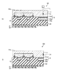
つぎに、このような構成の半導体装置の製造方法について説明する。図14−1〜図14−6は、第3の実施形態による半導体装置の製造方法の手順の一例を模式的に示す断面図である。まず。図14−1(a)に示されるように、半導体基板であるデバイスウェハ11の第1面11aに、STI(Shallow Trench Isolation)法などの方法によって、素子分離絶縁膜が形成される。また、素子分離絶縁膜60で区画される所定の領域にウェル注入を行って、Pウェル12PおよびNウェル12Nを形成する。
Next, a method of manufacturing a semiconductor device having such a configuration will be described. 14-1 to 14-6 are cross-sectional views schematically showing an example of a procedure of a method for manufacturing a semiconductor device according to a third embodiment. First. As shown in FIG. 14-1 (a), an element separation insulating film is formed on the
ついで、図14−1(b)に示されるように、素子分離絶縁膜が形成されたデバイスウェハ11の第1面11a上の全面にゲート絶縁膜51となる酸化シリコン膜511を形成する。その後、図14−2(c)に示されるように、デバイス配置領域Rdvをレジストパターンなどでマスクし、ダイシング領域Rd上に酸化シリコン膜512を形成する。ここでは、図14−1(b)と図14−2(c)で形成される酸化シリコン膜511,512の合計の膜厚が所定値となるように、酸化シリコン膜512を形成する。
Then, as shown in FIG. 14-1 (b), a
ついで、図14−2(d)に示されるように、酸化シリコン膜511,512上にゲート電極52の一部となるポリシリコン膜53を形成する。その後、図14−3(e)に示されるように、デバイス配置領域Rdvをレジストパターンなどでマスクし、ダイシング領域Rd上にポリシリコン膜532を形成する。ここでは、図14−2(d)と図14−3(e)で形成されるポリシリコン膜53,532の合計の膜厚が所定値となるように、ポリシリコン膜532を形成する。
Then, as shown in FIG. 14-2 (d), a
ついで、図14−3(f)に示されるように、ポリシリコン膜53,532上にゲート電極52の一部となるタングステン膜54を形成する。その後、図14−4(g)に示されるように、リソグラフィ技術およびエッチング技術を用いて、タングステン膜54、ポリシリコン膜53および酸化シリコン膜511を加工し、デバイス配置領域RdvのNウェルNW上およびPウェルPW上の所定の位置に所定の形状のゲート構造50を形成する。つまり、酸化シリコン膜511はゲート絶縁膜51となり、ポリシリコン膜53およびタングステン膜54はゲート電極52となる。そして、NウェルNW上およびPウェルPW上には、ゲート絶縁膜51およびゲート電極52が積層されたゲート構造50が形成される。また、ダイシング領域Rdでは、デバイスウェハ11とタングステン膜54との間に、酸化シリコン膜511,512およびポリシリコン膜53,532が積層された多層膜からなる反射率低減層13が形成される。なお、以下では、酸化シリコン膜511,512を合わせて酸化シリコン膜51aと表記し、ポリシリコン膜53,532を合わせてポリシリコン膜53aと表記する。
Then, as shown in FIG. 14-3 (f), a
ついで、図14−4(h)に示されるように、ゲート構造50をマスクとしてイオン注入を行い、NウェルNWにはP型不純物からなる高濃度拡散層からなるソース/ドレイン領域57を形成し、PウェルPWにはN型不純物からなる高濃度拡散層からなるソース/ドレイン領域57を形成する。これによって、NウェルNWにはNMOSトランジスタNTが形成され、PウェルPWにはPMOSトランジスタPTが形成される。その後、デバイスウェハ11上に、図示しない他の素子、配線層、および層間絶縁膜58などが形成され、デバイス層12が形成される。
Then, as shown in FIG. 14-4 (h), ion implantation was performed using the
デバイス層12が形成された後、図14−5(i)に示されるように、デバイス層12が形成されたデバイスウェハ11の第1面11a側にパッシベーション膜21を形成する。パッシベーション膜21は、例えばポリイミド膜である。また、パッシベーション膜21上にテープ22を貼りつける。
After the
ついで、図14−5(j)に示されるように、第2面側からデバイスウェハ11を所定の厚さになるまで研削を行う。例えば、30μm以下の厚さとなるまで裏面研削が行われる。
Then, as shown in FIG. 14-5 (j), the
その後、図14−6(k)に示されるように、ステルスダイシングによって、デバイスウェハ11のダイシング領域Rdに沿って、所定の間隔で改質層31を形成する。このとき、ダイシング領域Rdには、反射率低減層13が形成されているので、レーザ光Lのタングステン膜54aでの反射が抑えられ、タングステン膜54aで反射したレーザ光Lが改質層31の生成を阻害することがない。その結果、デバイスウェハ11の第2面11bから所望の深さに改質層31を形成することができる。
Then, as shown in FIG. 14-6 (k), the modified
そして、図14−6(l)に示されるように、改質層31が形成された後、テープを外周に向かって全体を引っ張る。これによって、チップ100に個片化される。以上によって、半導体装置が製造される。
Then, as shown in FIG. 14-6 (l), after the modified
なお、ここでは、ステルスダイシングで使用するレーザ光Lの波長が1,342nmである場合にレーザ光Lの反射率を抑制することができる多層膜について説明した。しかし、ステルスダイシングで使用するレーザ光Lの波長が変われば、それに応じて反射率低減層13の多層膜の構成は変わる。つまり、使用するレーザ光Lの波長に応じて、多層膜の種類および多層膜を構成する各膜の膜厚を変えればよい。
Here, a multilayer film capable of suppressing the reflectance of the laser beam L when the wavelength of the laser beam L used in stealth dicing is 1,342 nm has been described. However, if the wavelength of the laser beam L used in stealth dicing changes, the configuration of the multilayer film of the
第3の実施形態では、デバイスウェハ11と金属膜との間に、反射率低減層13として薄膜光学によって反射を抑制する多層膜を設けた。これによって、ステルスダイシング時のレーザ光Lの反射による改質層31の生成の阻害が抑制される。その結果、厚さの薄いデバイスウェハ11でも所望の位置に改質層31を形成することができ、デバイスウェハ11を個片化することができる。
In the third embodiment, a multilayer film that suppresses reflection by thin film optics is provided as a
また、デバイスウェハ11のデバイス配置領域RdvにCMOSトランジスタCTが配置される場合には、CMOSトランジスタCTで使用されるゲート絶縁膜51およびゲート電極52を構成するポリシリコン膜53からなる多層膜を反射率低減層13として利用することができる。その結果、ダイシング領域Rdにデバイス配置領域Rdvに配置されるデバイス層12の形成工程とは全く異なる多層膜の形成工程を導入する場合に比して、反射率低減層13を形成する手間を軽減することができる。
When the CMOS transistor CT is arranged in the device arrangement area Rdv of the
本発明のいくつかの実施形態を説明したが、これらの実施形態は、例として提示したものであり、発明の範囲を限定することは意図していない。これら新規な実施形態は、その他の様々な形態で実施されることが可能であり、発明の要旨を逸脱しない範囲で、種々の省略、置き換え、変更を行うことができる。これら実施形態やその変形は、発明の範囲や要旨に含まれるとともに、特許請求の範囲に記載された発明とその均等の範囲に含まれる。 Although some embodiments of the present invention have been described, these embodiments are presented as examples and are not intended to limit the scope of the invention. These novel embodiments can be implemented in various other embodiments, and various omissions, replacements, and changes can be made without departing from the gist of the invention. These embodiments and modifications thereof are included in the scope and gist of the invention, and are also included in the scope of the invention described in the claims and the equivalent scope thereof.
10 半導体装置、11 デバイスウェハ、11a 第1面、11b 第2面、12 デバイス層、13 反射率低減層、20 デバイス層、21 パッシベーション膜、22 テープ、30 集光点、31 改質層、32 ボイド、33 亀裂、50 ゲート構造、51 ゲート絶縁膜、51a 酸化シリコン膜、52 ゲート電極、53 ポリシリコン膜、54 タングステン膜、57 ソース/ドレイン領域、58 層間絶縁膜、60 素子分離絶縁膜、100 チップ、111 半導体基板。 10 Semiconductor device, 11 device wafer, 11a 1st surface, 11b 2nd surface, 12 device layer, 13 Reflectivity reduction layer, 20 device layer, 21 Passive film, 22 tape, 30 Condensing point, 31 Modified layer, 32 Void, 33 cracks, 50 gate structure, 51 gate insulating film, 51a silicon oxide film, 52 gate electrode, 53 polysilicon film, 54 tungsten film, 57 source / drain region, 58 interlayer insulating film, 60 element separation insulating film, 100 Chip, 111 semiconductor substrate.
Claims (10)
前記半導体基板の前記第1領域の周囲に設けられる第2領域の前記第1面上に配置され、前記第1面上に金属膜が配置された場合の前記第1面に対向する第2面側から入射されるレーザ光の反射率に比して反射率を低減する反射率低減層と、
前記第2領域の前記半導体基板の側面に設けられる改質層と、
を備え、
前記第2領域の前記半導体基板の側面は、前記半導体基板の中を伸展した切断面である半導体装置。 A device layer arranged on the first surface of the first region of the semiconductor substrate,
A second surface that is arranged on the first surface of a second region provided around the first region of the semiconductor substrate and faces the first surface when a metal film is arranged on the first surface. A reflectance reduction layer that reduces the reflectance compared to the reflectance of the laser beam incident from the side,
A modified layer provided on the side surface of the semiconductor substrate in the second region,
With
The side surface of the semiconductor substrate in the second region is a semiconductor device which is a cut surface extended in the semiconductor substrate.
前記半導体基板の前記第1面上に配置される絶縁膜と、
前記絶縁膜上に配置される半導体膜と、
を有する請求項3に記載の半導体装置。 The reflectance reducing layer is
An insulating film arranged on the first surface of the semiconductor substrate and
The semiconductor film arranged on the insulating film and
The semiconductor device according to claim 3.
前記ボイドの前記第1面側に最も近い位置は、前記第1面から6μmの範囲内に存在する請求項1から8のいずれか1つに記載の半導体装置。 The modified layer has a void and a crack arranged on the second surface side of the void facing the first surface.
The semiconductor device according to any one of claims 1 to 8, wherein the position closest to the first surface side of the void is within a range of 6 μm from the first surface.
前記半導体基板が所定の厚さとなるように、前記半導体基板の前記第1面に対向する第2面を研削し、
前記第2領域に沿って所定の周期でレーザ光を照射して、前記半導体基板の内部に改質層を形成し、
前記改質層に沿って、前記第1面側に亀裂を生成して前記半導体基板を個片化することを含み、
前記反射率低減層は、前記第1面上に金属膜が配置された場合の前記第2面側から入射されるレーザ光の反射率に比して反射率を低減する構成を有する半導体装置の製造方法。 A device layer is formed on the first region on the first surface of the semiconductor substrate, and a reflectance reducing layer is formed on the second region provided around the first region.
The second surface of the semiconductor substrate facing the first surface is ground so that the semiconductor substrate has a predetermined thickness.
A modified layer is formed inside the semiconductor substrate by irradiating a laser beam at a predetermined cycle along the second region.
Including cracking on the first surface side along the modified layer to individualize the semiconductor substrate.
The reflectance reducing layer is a semiconductor device having a configuration in which the reflectance is reduced as compared with the reflectance of laser light incident from the second surface side when the metal film is arranged on the first surface. Production method.
Priority Applications (4)
| Application Number | Priority Date | Filing Date | Title |
|---|---|---|---|
| JP2019047449A JP2020150168A (en) | 2019-03-14 | 2019-03-14 | Semiconductor device and manufacturing method thereof |
| TW108120745A TWI764006B (en) | 2019-03-14 | 2019-06-14 | Semiconductor device and manufacturing method of semiconductor device |
| CN201910589721.3A CN111696923B (en) | 2019-03-14 | 2019-07-02 | Semiconductor device and method for manufacturing semiconductor device |
| US16/559,552 US11139208B2 (en) | 2019-03-14 | 2019-09-03 | Semiconductor device and method of manufacturing semiconductor device |
Applications Claiming Priority (1)
| Application Number | Priority Date | Filing Date | Title |
|---|---|---|---|
| JP2019047449A JP2020150168A (en) | 2019-03-14 | 2019-03-14 | Semiconductor device and manufacturing method thereof |
Publications (1)
| Publication Number | Publication Date |
|---|---|
| JP2020150168A true JP2020150168A (en) | 2020-09-17 |
Family
ID=72423928
Family Applications (1)
| Application Number | Title | Priority Date | Filing Date |
|---|---|---|---|
| JP2019047449A Pending JP2020150168A (en) | 2019-03-14 | 2019-03-14 | Semiconductor device and manufacturing method thereof |
Country Status (4)
| Country | Link |
|---|---|
| US (1) | US11139208B2 (en) |
| JP (1) | JP2020150168A (en) |
| CN (1) | CN111696923B (en) |
| TW (1) | TWI764006B (en) |
Families Citing this family (3)
| Publication number | Priority date | Publication date | Assignee | Title |
|---|---|---|---|---|
| JP7358193B2 (en) * | 2019-10-28 | 2023-10-10 | 株式会社ディスコ | Wafer processing method |
| CN112537754B (en) * | 2020-12-08 | 2021-10-22 | 江苏创芯海微科技有限公司 | Electrical isolation structure and preparation method thereof |
| CN112537753B (en) * | 2020-12-08 | 2021-12-24 | 江苏创芯海微科技有限公司 | Scribing channel structure suitable for laser invisible cutting and preparation method thereof |
Family Cites Families (14)
| Publication number | Priority date | Publication date | Assignee | Title |
|---|---|---|---|---|
| EP1311892B1 (en) * | 2000-08-18 | 2004-11-03 | Koninklijke Philips Electronics N.V. | Optical component and method of manufacturing same |
| US20060022195A1 (en) * | 2004-08-01 | 2006-02-02 | Kun-Chih Wang | Scribe line structure |
| JP4198123B2 (en) * | 2005-03-22 | 2008-12-17 | 浜松ホトニクス株式会社 | Laser processing method |
| JP4809632B2 (en) * | 2005-06-01 | 2011-11-09 | ルネサスエレクトロニクス株式会社 | Manufacturing method of semiconductor device |
| TWI381485B (en) * | 2005-11-10 | 2013-01-01 | Renesas Electronics Corp | Semiconductor device manufacturing method and semiconductor device |
| JP4424302B2 (en) * | 2005-11-16 | 2010-03-03 | 株式会社デンソー | Manufacturing method of semiconductor chip |
| US20070111480A1 (en) * | 2005-11-16 | 2007-05-17 | Denso Corporation | Wafer product and processing method therefor |
| US7888236B2 (en) * | 2007-05-14 | 2011-02-15 | Taiwan Semiconductor Manufacturing Co., Ltd. | Semiconductor device and fabrication methods thereof |
| JP5054496B2 (en) | 2007-11-30 | 2012-10-24 | 浜松ホトニクス株式会社 | Processing object cutting method |
| JP5549403B2 (en) | 2010-06-16 | 2014-07-16 | 富士通セミコンダクター株式会社 | Manufacturing method of semiconductor device |
| JP2012069608A (en) * | 2010-09-21 | 2012-04-05 | Toshiba Corp | Semiconductor device and method of manufacturing the semiconductor device |
| US9171794B2 (en) * | 2012-10-09 | 2015-10-27 | Mc10, Inc. | Embedding thin chips in polymer |
| CN104968621A (en) * | 2013-02-04 | 2015-10-07 | 旭硝子株式会社 | Method for cutting glass substrate, glass substrate, near infrared ray cut filter glass and method for manufacturing glass substrate |
| JP6401009B2 (en) | 2014-10-15 | 2018-10-03 | 株式会社ディスコ | Wafer processing method |
-
2019
- 2019-03-14 JP JP2019047449A patent/JP2020150168A/en active Pending
- 2019-06-14 TW TW108120745A patent/TWI764006B/en active
- 2019-07-02 CN CN201910589721.3A patent/CN111696923B/en active Active
- 2019-09-03 US US16/559,552 patent/US11139208B2/en active Active
Also Published As
| Publication number | Publication date |
|---|---|
| CN111696923A (en) | 2020-09-22 |
| TWI764006B (en) | 2022-05-11 |
| US11139208B2 (en) | 2021-10-05 |
| US20200294856A1 (en) | 2020-09-17 |
| CN111696923B (en) | 2023-11-03 |
| TW202034539A (en) | 2020-09-16 |
Similar Documents
| Publication | Publication Date | Title |
|---|---|---|
| US11139208B2 (en) | Semiconductor device and method of manufacturing semiconductor device | |
| US9704835B2 (en) | Three dimensional integrated circuit | |
| US8461021B2 (en) | Multiple seal ring structure | |
| US10049915B2 (en) | Three dimensional integrated circuit | |
| JP2019054150A (en) | Semiconductor device manufacturing method and semiconductor wafer | |
| JPWO2018235843A1 (en) | Method of manufacturing semiconductor device and wafer sticking structure | |
| US10350711B2 (en) | Semiconductor device and manufacturing method thereof | |
| US10373855B2 (en) | Method for processing a wafer and method for processing a carrier | |
| JP5387451B2 (en) | Design method and manufacturing method of SOI wafer | |
| TWI707454B (en) | Semiconductor device | |
| JP4398420B2 (en) | Manufacturing method of semiconductor device | |
| TWI782062B (en) | Manufacturing method of laminated element | |
| CN106569386B (en) | Photomask and method for simultaneously preparing multiple chips by using photomask | |
| EP2242108A1 (en) | Semiconductor manufacturing method | |
| TWI699889B (en) | Semiconductor device | |
| US11854892B2 (en) | Substrate dicing method, method of fabricating semiconductor device, and semiconductor chip fabricated by them | |
| TW201729307A (en) | Manufacturing method of package structure | |
| TWI837690B (en) | Semiconductor devices and semiconductor manufacturing equipment | |
| US20230268363A1 (en) | Method for manufacturing an optical unit that comprises an array of organic microlenses | |
| US20230299025A1 (en) | Semiconductor device and semiconductor manufacturing apparatus | |
| US20200058485A1 (en) | Hydrogen ventilation of cmos wafers | |
| JP2010010716A (en) | Semiconductor device | |
| JP2003046071A (en) | Production method for semiconductor device | |
| JP2003257897A (en) | Method for manufacturing semiconductor chip | |
| CN113964177A (en) | Semiconductor wafer thinned by stealth laser irradiation |