JP2020076926A - Display device and imaging device - Google Patents
Display device and imaging device Download PDFInfo
- Publication number
- JP2020076926A JP2020076926A JP2018211701A JP2018211701A JP2020076926A JP 2020076926 A JP2020076926 A JP 2020076926A JP 2018211701 A JP2018211701 A JP 2018211701A JP 2018211701 A JP2018211701 A JP 2018211701A JP 2020076926 A JP2020076926 A JP 2020076926A
- Authority
- JP
- Japan
- Prior art keywords
- data
- display device
- holding unit
- pulses
- circuit
- Prior art date
- Legal status (The legal status is an assumption and is not a legal conclusion. Google has not performed a legal analysis and makes no representation as to the accuracy of the status listed.)
- Pending
Links
Images


Classifications
-
- G—PHYSICS
- G09—EDUCATION; CRYPTOGRAPHY; DISPLAY; ADVERTISING; SEALS
- G09G—ARRANGEMENTS OR CIRCUITS FOR CONTROL OF INDICATING DEVICES USING STATIC MEANS TO PRESENT VARIABLE INFORMATION
- G09G3/00—Control arrangements or circuits, of interest only in connection with visual indicators other than cathode-ray tubes
- G09G3/20—Control arrangements or circuits, of interest only in connection with visual indicators other than cathode-ray tubes for presentation of an assembly of a number of characters, e.g. a page, by composing the assembly by combination of individual elements arranged in a matrix no fixed position being assigned to or needed to be assigned to the individual characters or partial characters
- G09G3/2007—Display of intermediate tones
- G09G3/2014—Display of intermediate tones by modulation of the duration of a single pulse during which the logic level remains constant
-
- G—PHYSICS
- G09—EDUCATION; CRYPTOGRAPHY; DISPLAY; ADVERTISING; SEALS
- G09G—ARRANGEMENTS OR CIRCUITS FOR CONTROL OF INDICATING DEVICES USING STATIC MEANS TO PRESENT VARIABLE INFORMATION
- G09G3/00—Control arrangements or circuits, of interest only in connection with visual indicators other than cathode-ray tubes
- G09G3/20—Control arrangements or circuits, of interest only in connection with visual indicators other than cathode-ray tubes for presentation of an assembly of a number of characters, e.g. a page, by composing the assembly by combination of individual elements arranged in a matrix no fixed position being assigned to or needed to be assigned to the individual characters or partial characters
- G09G3/2003—Display of colours
-
- G—PHYSICS
- G09—EDUCATION; CRYPTOGRAPHY; DISPLAY; ADVERTISING; SEALS
- G09G—ARRANGEMENTS OR CIRCUITS FOR CONTROL OF INDICATING DEVICES USING STATIC MEANS TO PRESENT VARIABLE INFORMATION
- G09G2310/00—Command of the display device
- G09G2310/02—Addressing, scanning or driving the display screen or processing steps related thereto
- G09G2310/0264—Details of driving circuits
- G09G2310/027—Details of drivers for data electrodes, the drivers handling digital grey scale data, e.g. use of D/A converters
-
- G—PHYSICS
- G09—EDUCATION; CRYPTOGRAPHY; DISPLAY; ADVERTISING; SEALS
- G09G—ARRANGEMENTS OR CIRCUITS FOR CONTROL OF INDICATING DEVICES USING STATIC MEANS TO PRESENT VARIABLE INFORMATION
- G09G2310/00—Command of the display device
- G09G2310/02—Addressing, scanning or driving the display screen or processing steps related thereto
- G09G2310/0264—Details of driving circuits
- G09G2310/0275—Details of drivers for data electrodes, other than drivers for liquid crystal, plasma or OLED displays, not related to handling digital grey scale data or to communication of data to the pixels by means of a current
-
- G—PHYSICS
- G09—EDUCATION; CRYPTOGRAPHY; DISPLAY; ADVERTISING; SEALS
- G09G—ARRANGEMENTS OR CIRCUITS FOR CONTROL OF INDICATING DEVICES USING STATIC MEANS TO PRESENT VARIABLE INFORMATION
- G09G2310/00—Command of the display device
- G09G2310/02—Addressing, scanning or driving the display screen or processing steps related thereto
- G09G2310/0264—Details of driving circuits
- G09G2310/0294—Details of sampling or holding circuits arranged for use in a driver for data electrodes
-
- G—PHYSICS
- G09—EDUCATION; CRYPTOGRAPHY; DISPLAY; ADVERTISING; SEALS
- G09G—ARRANGEMENTS OR CIRCUITS FOR CONTROL OF INDICATING DEVICES USING STATIC MEANS TO PRESENT VARIABLE INFORMATION
- G09G2310/00—Command of the display device
- G09G2310/08—Details of timing specific for flat panels, other than clock recovery
-
- G—PHYSICS
- G09—EDUCATION; CRYPTOGRAPHY; DISPLAY; ADVERTISING; SEALS
- G09G—ARRANGEMENTS OR CIRCUITS FOR CONTROL OF INDICATING DEVICES USING STATIC MEANS TO PRESENT VARIABLE INFORMATION
- G09G2330/00—Aspects of power supply; Aspects of display protection and defect management
- G09G2330/02—Details of power systems and of start or stop of display operation
- G09G2330/025—Reduction of instantaneous peaks of current
Landscapes
- Engineering & Computer Science (AREA)
- Physics & Mathematics (AREA)
- Computer Hardware Design (AREA)
- General Physics & Mathematics (AREA)
- Theoretical Computer Science (AREA)
- Control Of Indicators Other Than Cathode Ray Tubes (AREA)
Abstract
Description
本発明は、表示装置および撮像装置に関する。 The present invention relates to a display device and an imaging device.
特許文献1には、複数の画素がマトリクス状に配置された有効表示部と、水平駆動回路と、垂直駆動回路とを有する表示装置が記載されている。垂直駆動回路は、シフトレジスタと、サンプリング回路群と、第2ラッチ回路群とを有する。シフトレジスタは、列を選択するサンプリングパルスを順次に発生する。サンプリング回路群は、シフトレジスタからのサンプリングパルスに応じてデジタル画像データを順次にサンプリングする。第2ラッチ回路群は、サンプリング回路群によってサンプリングされたデータ群を一括してラッチすることによって該データ群を線順次化する。
特許文献1に記載された表示装置では、サンプリング回路群によってサンプリングされたデータ群を第2ラッチ回路群が同時にラッチするので、最大過渡電流が大きくなりうる。最大過渡電流が大きいと、電源線の寄生抵抗による電圧降下が無視できなくなり、回路が誤動作する可能性がある。
In the display device described in
本発明は、第1保持部によって保持されたデータが第2保持部によって取り込まれる際の最大過渡電流を低減するために有利な技術を提供することを目的とする。 It is an object of the present invention to provide an advantageous technique for reducing the maximum transient current when the data held by the first holding unit is taken in by the second holding unit.
本発明の1つの側面によれば、複数の行および複数の列を構成するように配置された複数の画素と、前記複数の行における行を選択する行選択回路と、前記複数の画素のうち前記行選択回路によって選択された行の画素に信号を供給する信号供給回路と、を備える表示装置であって、前記信号供給回路は、複数の第1データ保持部を有する第1保持部と、前記複数の第1データ保持部を順に選択し、選択された第1データ保持部にデータを取り込ませる走査回路と、各ブロックが複数の第2データ保持部を有する複数のブロックを有し、前記第1保持部によって保持された複数のデータを時分割で取り込んで保持する第2保持部と、前記第2保持部によって保持された複数のデータに応じた複数のアナログ信号を前記複数の画素のうち前記行選択回路によって選択された行の画素に供給するDA変換部と、を含む。 According to one aspect of the present invention, a plurality of pixels arranged to form a plurality of rows and a plurality of columns, a row selection circuit that selects a row in the plurality of rows, and a plurality of pixels among the plurality of pixels. A signal supply circuit that supplies a signal to pixels in a row selected by the row selection circuit, wherein the signal supply circuit includes a first holding unit having a plurality of first data holding units; A scanning circuit that sequentially selects the plurality of first data holding units and loads data into the selected first data holding unit; and a plurality of blocks in which each block has a plurality of second data holding units, A second holding unit that captures and holds the plurality of data held by the first holding unit in a time division manner, and a plurality of analog signals corresponding to the plurality of data held by the second holding unit are stored in the plurality of pixels. And a DA converter that supplies the pixels of the row selected by the row selection circuit.
本発明によれば、第1保持部によって保持されたデータが第2保持部によって取り込まれる際の最大過渡電流を低減するために有利な技術が提供される。 According to the present invention, an advantageous technique is provided for reducing the maximum transient current when the data held by the first holding unit is fetched by the second holding unit.
以下、添付図面を参照しながら本発明をその例示的な実施形態を通して説明する。 Hereinafter, the present invention will be described through exemplary embodiments thereof with reference to the accompanying drawings.
図1には、本発明の一実施形態の表示装置1の構成が示されている。表示装置1は、画素アレイ10、垂直走査回路(行選択回路)20、信号供給回路30および制御回路40を備えうる。画素アレイ10は、複数の行および複数の列を構成するように配置された複数の画素11を有する。各画素11は、複数のサブ画素(例えば、R(赤)サブ画素、G(緑)サブ画素、B(青)サブ画素)を含みうる。垂直走査回路(行選択回路)20は、画素アレイ10の複数の行における行を選択する。行の選択は、垂直走査回路20が走査線21を介して、選択すべき行を構成する1行分の画素11(1行分のサブ画素)に制御信号を供給することによってなされる。信号供給回路30は、垂直走査回路20によって選択された行の1行分の画素11に信号線31を介して信号(輝度信号)を供給する。垂直走査回路20および信号供給回路30は、制御回路40によって制御されうる。
FIG. 1 shows the configuration of a
1つの信号線310は、1つの画素11を構成する複数のサブ画素(Rサブ画素、Gサブ画素、Bサブ画素)に対応する個数のサブ信号線を含みうる。以下では、説明の簡単化のために、画素アレイ10が6列(信号線310の数が6)で構成され、1つの信号線310が3つのサブ信号線(Rサブ画素用、Gサブ画素用、Bサブ画素用)で構成されるものとして説明する。しかし、実際には、画素アレイ10は、より多くの列を有しうる。また、1つの画素11を構成するサブ画素の個数は、3個に限定されない。
One signal line 310 may include a number of sub signal lines corresponding to a plurality of sub pixels (R sub pixel, G sub pixel, B sub pixel) included in one
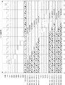
図2には、信号供給回路30の構成例が示されている。信号供給回路30は、走査回路201(シフトレジスタ)と、第1保持部202と、第2保持部203と、DA変換部(デジタル−アナログ変換部)204とを含みる。第1保持部202は、複数の第1データ保持部DH1−1、DH1−2、DH1−3、DH1−4、DH1−5、DH1−6を有する。ここで、文字列(例えば、DH1)に付される添え字”−x”(この例では、x=1〜6)は、画素アレイ10の列に対応する。例えば、DH1−1は、画素アレイ10の第1列に対応する第1データ保持部、即ち、画素アレイ10の第1列に信号を供給するための第1データ保持部である。以下では、列を特定する必要がない場合には、第1データ保持部DH1と記載する。各第1保持部DH1は、Rサブ画素、Gサブ画素、Bサブ画素に信号を供給するために、Rサブ画素用のラッチRL1、Gサブ画素用のラッチGL1、Bサブ画素用のラッチGL1を含みうる。
FIG. 2 shows a configuration example of the
第2保持部203は、複数のブロックBLK1、BLK2を含み、各ブロックは、複数の第2データ保持部DH2を有する。例えば、第1ブロックBLK1は、複数の第2データ保持部DH2として、第2データ保持部DH2−1、DH2−2、DH2−3を有する。また、第2ブロックBLK2は、複数の第2データ保持部DH2として、第2データ保持部DH2−4、DH−5、DH−6を有する。第2保持部203は、第1保持部202によって保持された複数のデータを時分割で取り込んで保持する。別の観点において、複数のブロックBLK1、BLK2の各々は、第1保持部202によって保持された複数のデータを時分割で取り込んで保持する。各第2データ保持部DH2は、Rサブ画素、Gサブ画素、Bサブ画素に信号を供給するために、Rサブ画素用のラッチRL2、Gサブ画素用のラッチGL2、Bサブ画素用のラッチGL2を含みうる。
The
第1保持部202および第2保持部203によって2段の保持部が構成される。制御回路40から供給される輝度データ(この例では、RデータRD0、GデータGD0、BデータBD0で構成される。)の取り込みおよび保持を第1保持部202が担い、DA変換部204への輝度データ(この例では、RデータRD2、GデータGD2、BデータBD2で構成される。)の供給を第2保持部203が担う。このような構成では、輝度データの取り込み動作と供給動作とを並行して行うことができるので、高速化に有利である。
The
走査回路201は、第1保持部202の複数の第1データ保持部DH1を順に選択し、選択された第1データ保持部DH1にデータを取り込ませる。走査回路201は、シフトレジスタで構成されうる。該シフトレジスタは、制御回路40から供給されるスタートパルスP_STを受けてパルスを順次に後段に転送するように直列接続された6個(6段)のフリップフロップFFで構成されうる。該シフトレジスタは、複数のフリップフロップFFがクロック信号CLKに同期してパルスを順次に転送するように構成されうる。各フリップフロップFFは、制御回路40から供給されるリセット信号RESBによってリセットされうる。クロック信号CLKは、例えば、外部装置または表示装置1において生成される基準クロック信号に基づいて制御回路40によって生成されうる。走査回路201は、6個のフリップフロップFFのそれぞれからの出力信号を書き込みパルスHSR1〜HSR6として出力しうる。DA変換部204は、第2保持部203によって保持された複数のデータに応じた複数のアナログ信号を複数の画素11のうち垂直走査回路(行選択回路)20によって選択された行の画素11に供給しうる。
The
制御回路40は、輝度データとして、RデータRD0、GデータGD0、BデータBD0を信号供給回路30の第1保持部202に供給しうる。第1保持部202は、書き込みパルスHSR1〜HSR6に応じて、RデータRD0、GデータGD0、BデータBD0を取り込んで保持する。ここで、第1保持部202において、第1データ保持部DH1−xは、書き込みパルスHSRx(x=1〜6)に応じてRデータRD0、GデータGD0、BデータBD0を取り込んで保持し、RデータRD1、GデータGD1、BデータBD1として出力する。第2保持部203において、第2データ保持部DH2は、書き込みパルスPLAT1〜PLAT3に応じて、RデータRD1、GデータGD1、BデータBD1を取り込んで保持し、RデータRD2、GデータGD2、BデータBD2として出力する。制御回路40は、書き込みパルスPLAT1〜PLAT3を発生するパルス発生回路41を含みうる。パルス発生回路41は、信号供給回路30に備えられてもよい。
The
図3には、第1実施形態に信号供給回路30の動作が例示されている。時刻t0において、リセット信号REBがアクティブレベル(ローレベル)に遷移し、これにより、走査回路201のシフトレジスタを構成する6段のフリップフロップFFの出力である書き込みパルスHSR1〜HSR6がリセットされる。その後、リセット信号REBがインアクティブレベル(ハイレベル)に遷移した後、時刻t1からクロック信号CLKの供給が開始される。制御回路40は、時刻t1を含む期間においてアクティブレベルになるスタートパルスP_STを走査回路201に供給する。走査回路201は、クロック信号CLKに同期してパルス信号を順次に後段に転送することによって、互いに重複しない書き込みパルスHSR1〜HSR6を発生する。
FIG. 3 illustrates the operation of the
時刻t1から時刻t2において書き込みパルスHSR1がアクティブレベルとなり、第1保持部202の第1データ保持部DH1−1(RL1−1、GL1−1、BL1−1)によって、RデータRD0、GデータRD0、BデータBD0が取り込まれ保持される。時刻t2から時刻t3において書き込みパルスHSR2がアクティブレベルとなり、第1保持部202の第1データ保持部DH1−2(RL1−2、GL1−2、BL1−2)によって、RデータRD0、GデータRD0、BデータBD0が取り込まれ保持される。
From time t1 to time t2, the write pulse HSR1 becomes an active level, and the first data holding unit DH1-1 (RL1-1, GL1-1, BL1-1) of the
時刻t3から時刻t4において書き込みパルスHSR3がアクティブレベルとなり、第1保持部202の第1データ保持部DH1−3(RL1−3、GL1−3、BL1−3)によって、RデータRD0、GデータRD0、BデータBD0が取り込まれ保持される。時刻t4から時刻t5において書き込みパルスHSR4がアクティブレベルとなり、第1保持部202の第1データ保持部DH1−4(RL1−4、GL1−4、BL1−4)によって、RデータRD0、GデータRD0、BデータBD0が取り込まれ保持される。
From time t3 to time t4, the write pulse HSR3 becomes the active level, and the first data holding units DH1-3 (RL1-3, GL1-3, BL1-3) of the
時刻t5から時刻t6において書き込みパルスHSR1がアクティブレベルとなり、第1保持部202の第1データ保持部DH1−5(RL1−5、GL1−5、BL1−5)によって、RデータRD0、GデータRD0、BデータBD0が取り込まれ保持される。時刻t6から時刻t7において書き込みパルスHSR2がアクティブレベルとなり、第1保持部202の第1データ保持部DH1−6(RL1−6、GL1−6、BL1−6)によって、RデータRD0、GデータRD0、BデータBD0が取り込まれ保持される。
From time t5 to time t6, the write pulse HSR1 becomes the active level, and the first data holding units DH1-5 (RL1-5, GL1-5, BL1-5) of the
その後、パルス発生回路41は、時刻t8〜t10において書き込みパルスPLAT1をアクティブレベルとする。したがって、時刻t8〜t10において、第2保持部203の第1ブロックBLK1における第2データ保持部DH2−1によって、それに対応するRデータRD1−1、GデータRD1−1、BデータBD1−1が取り込まれ保持される。また、時刻t8〜t10において、第2保持部203の第2ブロックBLK2における第2データ保持部DH2−4によって、それに対応するRデータRD1−4、GデータRD1−4、BデータBD1−4が取り込まれ保持される。このように、第1ブロックBLK1における第2データ保持部DH2−1および第2ブロックBLK2における第2データ保持部DH2−4によるデータの取り込み動作が書き込みパルスPLAT1に従って同時になされうる。パルス発生回路41は、例えば、書き込み信号HSR6に応答して生成されるタイミング信号PLATに応じて書き込みパルスPLAT1を発生しうる。あるいは、パルス発生回路41は、例えば、書き込み信号HSR6に応答して書き込みパルスPLAT1、PLAT2、PLAT3を発生しうる。
After that, the pulse generation circuit 41 sets the write pulse PLAT1 to the active level from time t8 to t10. Therefore, from time t8 to t10, the second data holding unit DH2-1 in the first block BLK1 of the
パルス発生回路41は、時刻t11〜t13において書き込みパルスPLAT2をアクティブレベルとする。したがって、時刻t11〜t13において、第2保持部203の第1ブロックBLK1における第2データ保持部DH2−2によって、それに対応するRデータRD1−2、GデータRD1−2、BデータBD1−2が取り込まれ保持される。また、時刻t11〜t13において、第2保持部203の第2ブロックBLK2における第2データ保持部DH2−5によって、それに対応するRデータRD1−5、GデータRD1−5、BデータBD1−5が取り込まれ保持される。このように、第1ブロックBLK1における第2データ保持部DH2−2および第2ブロックBLK2における第2データ保持部DH2−5によるデータの取り込み動作が書き込みパルスPLAT2に従って同時になされうる。
The pulse generation circuit 41 sets the write pulse PLAT2 to the active level from time t11 to time t13. Therefore, at times t11 to t13, the corresponding R data RD1-2, G data RD1-2, and B data BD1-2 are generated by the second data holding unit DH2-2 in the first block BLK1 of the
パルス発生回路41は、時刻t14〜t16において書き込みパルスPLAT3をアクティブレベルとする。したがって、時刻t14〜t16において、第2保持部203の第1ブロックBLK1における第2データ保持部DH2−3によって、それに対応するRデータRD1−3、GデータRD1−3、BデータBD1−3が取り込まれ保持される。また、時刻t14〜t16において、第2保持部203の第2ブロックBLK2における第2データ保持部DH2−6によって、それに対応するRデータRD1−6、GデータRD1−6、BデータBD1−6が取り込まれ保持される。このように、第1ブロックBLK1における第2データ保持部DH2−3および第3ブロックBLK2における第2データ保持部DH2−6によるデータの取り込み動作が書き込みパルスPLAT3に従って同時になされうる。
The pulse generation circuit 41 sets the write pulse PLAT3 to the active level from time t14 to t16. Therefore, from the time t14 to t16, the R data RD1-3, G data RD1-3, and B data BD1-3 corresponding to the second data holding unit DH2-3 in the first block BLK1 of the
以上のように、パルス発生回路41は、第1保持部202によって保持された複数のデータが第2保持部203によって時分割で取り込まれるように書き込みパルスPLAT1〜PLAT3を発生する。ここで、複数のブロックのうち1つのブロックが第1保持部によって保持された複数のデータのうち対応するデータを取り込むことに並行して複数のブロックのうち他のブロックが第1保持部によって保持された複数のデータのうち対応するデータを取り込む。その後、DA変換部204は、第2保持部203によって保持されたデータRD2、GD2、BD2に応じたアナログ信号を複数の画素11のうち垂直走査回路(行選択回路)20によって選択された行の画素11に供給する。これにより、垂直走査回路20によって選択された行の画素11にアナログ信号が書き込まれる。
As described above, the pulse generation circuit 41 generates the write pulses PLAT1 to PLAT3 so that the plurality of data held by the
以上のように、パルス発生回路41は、複数の書き込みパルスPLAT1、PLAT2、PLAT3のそれぞれのアクティブ期間が互いに重複しないように複数のパルスPLAT1、PLAT2、PLAT3を発生する。換言すると、パルス発生回路41は、複数の書き込みパルスPLAT1、PLAT2、PLAT3の遷移タイミングが同一タイミングにならないように複数のパルスPLAT1、PLAT2、PLAT3を発生する。これにより、複数の書き込みパルスPLAT1、PLAT2、PLAT3の遷移時に大きな過渡電流が流れることを防止し、信号供給回路30の電源線と接地線との間に流れる最大過渡電流を抑えることができる。
As described above, the pulse generation circuit 41 generates the plurality of pulses PLAT1, PLAT2, PLAT3 so that the active periods of the plurality of write pulses PLAT1, PLAT2, PLAT3 do not overlap each other. In other words, the pulse generation circuit 41 generates the plurality of pulses PLAT1, PLAT2, PLAT3 so that the transition timings of the plurality of write pulses PLAT1, PLAT2, PLAT3 do not become the same timing. As a result, it is possible to prevent a large transient current from flowing during the transition of the plurality of write pulses PLAT1, PLAT2, and PLAT3, and to suppress the maximum transient current flowing between the power supply line and the ground line of the
複数のブロックBLK1、BLK2のそれぞれに含まれる第2データ保持部DH2の個数は、複数のブロックブロックBLK1、BLK2において同一にされうる。これにより、前述の過渡電流を均一化することができる。パルス発生回路41は、複数の書き込みパルスPLAT1〜PLAT3のそれぞれのアクティブ期間の長さが互いに等しいように複数の書き込みパルスPLAT1〜PLAT3を発生しうる。パルス発生回路41は、複数の書き込みパルスPLAT1〜PLAT3の各々のアクティブ期間が書き込みパルスHSR1〜HSR6のアクティブ期間より長いように、複数の書き込みパルスPLAT1〜PLAT3を発生しうる。複数の書き込みパルスPLAT1〜PLAT3の個数は、例えば、複数のブロックBLK1、BLK2の各々を構成する第2データ保持部DH2の個数(列数)と等しく設定されうる。 The number of the second data holding units DH2 included in each of the blocks BLK1 and BLK2 may be the same in the block blocks BLK1 and BLK2. As a result, the above-mentioned transient current can be made uniform. The pulse generation circuit 41 can generate the plurality of write pulses PLAT1 to PLAT3 so that the active periods of the plurality of write pulses PLAT1 to PLAT3 are equal to each other. The pulse generation circuit 41 can generate the plurality of write pulses PLAT1 to PLAT3 such that the active periods of the plurality of write pulses PLAT1 to PLAT3 are longer than the active periods of the write pulses HSR1 to HSR6. The number of the plurality of write pulses PLAT1 to PLAT3 can be set equal to, for example, the number (the number of columns) of the second data holding units DH2 configuring each of the plurality of blocks BLK1 and BLK2.
上記の実施形態では、走査回路201が第1保持部202の複数の第1データ保持部DH1の全てにデータを取り込ませる動作を行う期間(t0〜t7)の終了後に、第1保持部202によって取り込まれたデータを第2保持部202が取り込む動作が実行される。しかし、走査回路201が第1保持部202の複数の第1データ保持部DH1の全てにデータを取り込ませる動作を行う期間の終了前に、当該期間において第1保持部202によって既に取り込まれたデータを第2保持部203が取り込む動作が開始されてもよい。例えば、第2保持部203の複数のブロックBLK1、BLK2のうちの1つのブロックに供給するべき一群のデータが第1保持部202によって取り込まれる度に、該一群のデータが第2保持部203によって取り込まれうる。より具体的には、例えば、時刻t5の後に書き込みパルスPLAT1がアクティブレベルにされ、時刻t5の後に書き込みパルスPLAT2がアクティブレベルにされうる。ただし、複数の書き込みパルスPLAT1、PLAT2、PLAT3のそれぞれのアクティブ期間は、互いに重複しないように複数の書き込みパルスPLAT1、PLAT2、PLAT3が生成される。
In the above embodiment, after the period (t0 to t7) in which the
図4には、第2実施形態における信号供給回路30の動作が例示されている。図4に示された例では、パルス発生回路41は、複数の書き込みパルスPLAT1〜PLAT3における互いに連続する書き込みパルス同士が互いに部分的に重複するアクティブ期間を有するように複数のパルスPLAT1〜PLAT3を発生する。アクティブ期間が部分的に互いに重複するとは、1つのアクティブ期間の一部と他のアクティブ期間の一部とが重複することを意味する。
FIG. 4 illustrates the operation of the
図4に示された第2実施形態における時刻t0〜t8の動作は、図3に示された第1実施形態における時刻t0〜t8の動作と同一である。パルス発生回路41は、時刻t8〜t11において書き込みパルスPLAT1をアクティブレベルとする。したがって、時刻t8〜t11において、第2保持部203の第1ブロックBLK1における第2データ保持部DH2−1によって、それに対応するRデータRD1−1、GデータRD1−1、BデータBD1−1が取り込まれ保持される。また、時刻t8〜t11において、第2保持部203の第2ブロックBLK2における第2データ保持部DH2−4によって、それに対応するRデータRD1−4、GデータRD1−4、BデータBD1−4が取り込まれ保持される。このように、第1ブロックBLK1における第2データ保持部DH2−1および第2ブロックBLK2における第2データ保持部DH2−4によるデータの取り込み動作が書き込みパルスPLAT1に従って同時になされうる。
The operation from time t0 to t8 in the second embodiment shown in FIG. 4 is the same as the operation from time t0 to t8 in the first embodiment shown in FIG. The pulse generation circuit 41 sets the write pulse PLAT1 to the active level from time t8 to t11. Therefore, from time t8 to t11, the second data holding unit DH2-1 in the first block BLK1 of the
パルス発生回路41は、書き込みパルスPLAT2のアクティブ期間の一部が書き込みパルスPKAT1のアクティブ期間の一部と重複するように、時刻t9〜t11において書き込みパルスPLAT2をアクティブレベルとする。したがって、時刻t9〜t11において、第2保持部203の第1ブロックBLK1における第2データ保持部DH2−2によって、それに対応するRデータRD1−2、GデータRD1−2、BデータBD1−2が取り込まれ保持される。また、時刻t9〜t11において、第2保持部203の第2ブロックBLK2における第2データ保持部DH2−5によって、それに対応するRデータRD1−5、GデータRD1−5、BデータBD1−5が取り込まれ保持される。このように、第1ブロックBLK1における第2データ保持部DH2−2および第2ブロックBLK2における第2データ保持部DH2−5によるデータの取り込み動作が書き込みパルスPLAT2に従って同時に、あるいは並行してなされうる。
The pulse generation circuit 41 sets the write pulse PLAT2 to the active level from time t9 to t11 so that a part of the active period of the write pulse PLAT2 overlaps with a part of the active period of the write pulse PKAT1. Therefore, from time t9 to t11, the second data holding unit DH2-2 in the first block BLK1 of the
パルス発生回路41は、書き込みパルスPLAT3のアクティブ期間の一部が書き込みパルスPKAT2のアクティブ期間の一部と重複するように、時刻t10〜t13において書き込みパルスPLAT3をアクティブレベルとする。したがって、時刻t10〜t13において、第2保持部203の第1ブロックBLK1における第2データ保持部DH2−3によって、それに対応するRデータRD1−3、GデータRD1−3、BデータBD1−3が取り込まれ保持される。また、時刻t10〜t13において、第2保持部203の第2ブロックBLK2における第2データ保持部DH2−6によって、それに対応するRデータRD1−6、GデータRD1−6、BデータBD1−6が取り込まれ保持される。このように、第1ブロックBLK1における第2データ保持部DH2−3および第2ブロックBLK2における第2データ保持部DH2−6によるデータの取り込み動作が書き込みパルスPLAT3に従って同時になされうる。パルス発生回路41は、3以上の書き込みパルスPLAT1〜PLAT3のそれぞれのアクティブ期間の一部が重複するように書き込みパルスPLAT1〜PLAT3を発生してもよい。
The pulse generation circuit 41 sets the write pulse PLAT3 to the active level at times t10 to t13 so that part of the active period of the write pulse PLAT3 overlaps with part of the active period of the write pulse PKAT2. Therefore, at times t10 to t13, the corresponding R data RD1-3, G data RD1-3, and B data BD1-3 are generated by the second data holding unit DH2-3 in the first block BLK1 of the
以上のように、パルス発生回路41は、第1保持部202によって保持された複数のデータが第2保持部203によって時分割で取り込まれるように書き込みパルスPLAT1〜PLAT3を発生する。ここで、複数のブロックのうち1つのブロックが第1保持部によって保持された複数のデータのうち対応するデータを取り込むことに並行して複数のブロックのうち他のブロックが第1保持部によって保持された複数のデータのうち対応するデータを取り込む。その後、DA変換部204は、第2保持部203によって保持されたデータRD2、GD2、BD2に応じたアナログ信号を複数の画素11のうち垂直走査回路(行選択回路)20によって選択された行の画素11に供給する。これにより、垂直走査回路20によって選択された行の画素11にアナログ信号が書き込まれる。第2実施形態は、最大過渡電流の抑制の他、1水平走査期間を短くするために有利である。
As described above, the pulse generation circuit 41 generates the write pulses PLAT1 to PLAT3 so that the plurality of data held by the
第2実施形態においても、パルス発生回路41は、複数の書き込みパルスPLAT1〜PLAT3のそれぞれのアクティブ期間の長さが互いに等しいように複数の書き込みパルスPLAT1〜PLAT3を発生しうる。また、パルス発生回路41は、複数の書き込みパルスPLAT1〜PLAT3の各々のアクティブ期間が書き込みパルスHSR1〜HSR6のアクティブ期間より長いように、複数の書き込みパルスPLAT1〜PLAT3を発生しうる。また、パルス発生回路41は、各書き込みパルスが他の書き込みパルスのアクティブ期間と重複している期間の長さが複数の書き込みパルスPLAT1〜PLAT3互いに等しいように複数の書き込みパルスPLAT1〜PLAT3を発生しうる。 Also in the second embodiment, the pulse generation circuit 41 can generate the plurality of write pulses PLAT1 to PLAT3 such that the active periods of the plurality of write pulses PLAT1 to PLAT3 are equal to each other. Further, the pulse generation circuit 41 can generate the plurality of write pulses PLAT1 to PLAT3 such that the active periods of the plurality of write pulses PLAT1 to PLAT3 are longer than the active periods of the write pulses HSR1 to HSR6. The pulse generation circuit 41 also generates a plurality of write pulses PLAT1 to PLAT3 such that the length of the period in which each write pulse overlaps the active period of another write pulse is equal to the plurality of write pulses PLAT1 to PLAT3. sell.
走査回路201が第1保持部202の複数の第1データ保持部DH1の全てにデータを取り込ませる動作を行う期間の終了前に、当該期間において第1保持部202によって既に取り込まれたデータを第2保持部203が取り込む動作が開始されてもよい。例えば、第2保持部203の複数のブロックBLK1、BLK2のうちの1つのブロックに供給するべき一群のデータが第1保持部202によって取り込まれる度に、該一群のデータが第2保持部203によって取り込まれうる。より具体的には、例えば、時刻t5の後に書き込みパルスPLAT1がアクティブレベルにされ、時刻t6の後に書き込みパルスPLAT2がアクティブレベルにされうる。ただし、複数の書き込みパルスPLAT1〜PLAT3における互いに連続する書き込みパルス同士が互いに部分的に重複するアクティブ期間を有するように複数の書き込みパルスPLAT1、PLAT2、PLAT3が生成される。
Before the end of the period in which the
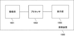
図5には、上記の実施形態の表示装置1に代表される表示部1003が組み込まれた撮像装置1000の構成が例示されている。撮像装置1000は、撮像部(イメージセンサ)1001と、撮像部1001によって撮像された画像を処理する処理部1002と、処理部1002によって処理された画像を表示する表示部1003とを備えうる。表示部1003は、例えば、撮像部1001によって撮像され処理部1002によって処理された画像の他、撮像装置1000の操作のための情報が表示されうる。撮像装置の概念には、撮像機能を有するあらゆる装置が含まれうる。表示部1003は、例えば、デジタルスチルカメラに代表される撮像装置の背面表示部であってもよいし、ビューファインダーであってよいし、その他の部分に設けられた表示部であってもよい。ビューファインダーは、撮像装置のファインダの中に配置されている表示装置である。
FIG. 5 exemplifies the configuration of the
1:表示装置、10:画素アレイ、11:画素、20:垂直走査回路(行選択回路)、30:信号供給回路、201:走査回路、202:第1保持部、203:第2保持部、204:DA変換部、DH1:第1データ保持部、DH2:第2データ保持部 1: display device, 10: pixel array, 11: pixel, 20: vertical scanning circuit (row selection circuit), 30: signal supply circuit, 201: scanning circuit, 202: first holding unit, 203: second holding unit, 204: DA conversion unit, DH1: first data holding unit, DH2: second data holding unit
Claims (14)
複数の第1データ保持部を有する第1保持部と、
前記複数の第1データ保持部を順に選択し、選択された第1データ保持部にデータを取り込ませる走査回路と、
各ブロックが複数の第2データ保持部を有する複数のブロックを有し、前記第1保持部によって保持された複数のデータを時分割で取り込んで保持する第2保持部と、
前記第2保持部によって保持された複数のデータに応じた複数のアナログ信号を前記複数の画素のうち前記行選択回路によって選択された行の画素に供給するDA変換部と、を含む、
ことを特徴とする表示装置。 A plurality of pixels arranged to form a plurality of rows and a plurality of columns, a row selection circuit that selects rows in the plurality of rows, and a row selection circuit of the plurality of pixels that is selected by the row selection circuit. A signal supply circuit that supplies a signal to a pixel, wherein the signal supply circuit comprises:
A first holding unit having a plurality of first data holding units;
A scanning circuit for sequentially selecting the plurality of first data holding units and loading data into the selected first data holding units;
A second holding unit in which each block has a plurality of blocks having a plurality of second data holding units, and which holds the plurality of data held by the first holding unit by time division
And a DA converter that supplies a plurality of analog signals corresponding to the plurality of data held by the second holding unit to the pixels in the row selected by the row selection circuit among the plurality of pixels.
A display device characterized by the above.
ことを特徴とする請求項1に記載の表示装置。 Each of the plurality of blocks fetches and holds corresponding data among the plurality of data held by the first holding unit in a time division manner,
The display device according to claim 1, wherein the display device is a display device.
ことを特徴とする請求項2に記載の表示装置。 While one block of the plurality of blocks fetches corresponding data of the plurality of data held by the first holding unit, another block of the plurality of blocks is loaded by the first holding unit. Retrieve the corresponding data from the multiple data stored by
The display device according to claim 2, wherein:
ことを特徴とする請求項1乃至3のいずれか1項に記載の表示装置。 The number of the second data holding units included in each of the plurality of blocks is the same in the plurality of blocks,
The display device according to claim 1, wherein the display device is a display device.
前記パルス発生回路は、前記複数のパルスのそれぞれのアクティブ期間が互いに重複しないように前記複数のパルスを発生する、
ことを特徴とする請求項1乃至4のいずれか1項に記載の表示装置。 Further comprising a pulse generating circuit for generating a plurality of pulses for capturing data in each of the plurality of blocks,
The pulse generation circuit generates the plurality of pulses so that respective active periods of the plurality of pulses do not overlap each other,
The display device according to claim 1, wherein the display device is a display device.
ことを特徴とする請求項5に記載の表示装置。 The lengths of the active periods of each of the plurality of pulses are equal to each other,
The display device according to claim 5, wherein:
前記パルス発生回路は、前記複数のパルスにおける互いに連続するパルス同士が互いに部分的に重複するアクティブ期間を有するように前記複数のパルスを発生する、
ことを特徴とする請求項1乃至6のいずれか1項に記載の表示装置。 Further comprising a pulse generating circuit for generating a plurality of pulses for capturing data in each of the plurality of blocks,
The pulse generation circuit generates the plurality of pulses such that consecutive pulses of the plurality of pulses have active periods in which they partially overlap with each other.
The display device according to claim 1, wherein the display device is a display device.
ことを特徴とする請求項7に記載の表示装置。 The lengths of the active periods of each of the plurality of pulses are equal to each other,
The display device according to claim 7, wherein:
ことを特徴とする請求項7又は8に記載の表示装置。 The length of the period in which the active period of each pulse overlaps the active period of another pulse is equal to each other in the plurality of pulses,
The display device according to claim 7, wherein the display device is a display device.
ことを特徴とする請求項5乃至9のいずれか1項に記載の表示装置。 An active period of each of the plurality of pulses generated by the pulse generation circuit is longer than an active period of a pulse for causing the scanning circuit to capture data in the first holding unit,
The display device according to claim 5, wherein the display device is a display device.
ことを特徴とする請求項1乃至10のいずれか1項に記載の表示装置。 After the end of the period in which the scanning circuit takes in the data to all of the plurality of first data holding units, the operation to take in the data taken in by the first holding unit is executed. ,
The display device according to claim 1, wherein the display device is a display device.
ことを特徴とする請求項1乃至10のいずれか1項に記載の表示装置。 Before the end of the period in which the scanning circuit takes in the data in all of the plurality of first data holding units, the second holding unit takes in the data already taken in by the first holding unit in the period. Operation is started,
The display device according to claim 1, wherein the display device is a display device.
ことを特徴とする請求項12に記載の表示装置。 Each time the group of data to be supplied to one of the plurality of blocks of the second holding unit is loaded by the first holding unit, the group of data is loaded by the second holding unit.
The display device according to claim 12, wherein:
前記撮像部によって撮像された画像を処理する処理部と、
前記処理部によって処理された画像を表示する表示部として構成された請求項1乃至13のいずれか1項に記載の表示装置と、
を備えることを特徴とする撮像装置。 An imaging unit,
A processing unit that processes the image captured by the image capturing unit;
The display device according to any one of claims 1 to 13, which is configured as a display unit that displays an image processed by the processing unit,
An imaging device comprising:
Priority Applications (2)
| Application Number | Priority Date | Filing Date | Title |
|---|---|---|---|
| JP2018211701A JP2020076926A (en) | 2018-11-09 | 2018-11-09 | Display device and imaging device |
| US16/676,738 US11120728B2 (en) | 2018-11-09 | 2019-11-07 | Display device and image capturing device |
Applications Claiming Priority (1)
| Application Number | Priority Date | Filing Date | Title |
|---|---|---|---|
| JP2018211701A JP2020076926A (en) | 2018-11-09 | 2018-11-09 | Display device and imaging device |
Publications (2)
| Publication Number | Publication Date |
|---|---|
| JP2020076926A true JP2020076926A (en) | 2020-05-21 |
| JP2020076926A5 JP2020076926A5 (en) | 2021-12-16 |
Family
ID=70550675
Family Applications (1)
| Application Number | Title | Priority Date | Filing Date |
|---|---|---|---|
| JP2018211701A Pending JP2020076926A (en) | 2018-11-09 | 2018-11-09 | Display device and imaging device |
Country Status (2)
| Country | Link |
|---|---|
| US (1) | US11120728B2 (en) |
| JP (1) | JP2020076926A (en) |
Families Citing this family (3)
| Publication number | Priority date | Publication date | Assignee | Title |
|---|---|---|---|---|
| CN114938418A (en) * | 2021-02-04 | 2022-08-23 | 佳能株式会社 | Viewfinder unit having line-of-sight detection function, image pickup apparatus, and attachment accessory |
| US20230176377A1 (en) * | 2021-12-06 | 2023-06-08 | Facebook Technologies, Llc | Directional illuminator and display apparatus with switchable diffuser |
| US12061343B2 (en) | 2022-05-12 | 2024-08-13 | Meta Platforms Technologies, Llc | Field of view expansion by image light redirection |
Citations (2)
| Publication number | Priority date | Publication date | Assignee | Title |
|---|---|---|---|---|
| US20080117190A1 (en) * | 2006-11-22 | 2008-05-22 | Chien-Ru Chen | Method and driver for driving a display |
| JP2010122602A (en) * | 2008-11-21 | 2010-06-03 | Oki Semiconductor Co Ltd | Driving apparatus of display panel |
Family Cites Families (5)
| Publication number | Priority date | Publication date | Assignee | Title |
|---|---|---|---|---|
| JP2005017988A (en) * | 2003-06-30 | 2005-01-20 | Sony Corp | Flat display device |
| JP4492334B2 (en) | 2004-12-10 | 2010-06-30 | ソニー株式会社 | Display device and portable terminal |
| JP5379194B2 (en) | 2011-08-09 | 2013-12-25 | 株式会社ジャパンディスプレイ | Display device |
| JP2013228460A (en) | 2012-04-24 | 2013-11-07 | Japan Display Inc | Display device |
| JP7141241B2 (en) | 2018-05-17 | 2022-09-22 | キヤノン株式会社 | Display device |
-
2018
- 2018-11-09 JP JP2018211701A patent/JP2020076926A/en active Pending
-
2019
- 2019-11-07 US US16/676,738 patent/US11120728B2/en active Active
Patent Citations (2)
| Publication number | Priority date | Publication date | Assignee | Title |
|---|---|---|---|---|
| US20080117190A1 (en) * | 2006-11-22 | 2008-05-22 | Chien-Ru Chen | Method and driver for driving a display |
| JP2010122602A (en) * | 2008-11-21 | 2010-06-03 | Oki Semiconductor Co Ltd | Driving apparatus of display panel |
Also Published As
| Publication number | Publication date |
|---|---|
| US11120728B2 (en) | 2021-09-14 |
| US20200152110A1 (en) | 2020-05-14 |
Similar Documents
| Publication | Publication Date | Title |
|---|---|---|
| US11363230B2 (en) | Image sensor module and image sensor device including the same | |
| JP5917055B2 (en) | Solid-state imaging device, driving method thereof, and control program | |
| US20200258463A1 (en) | Shift register unit, gate drive circuit and method of driving the same | |
| JP2020076926A (en) | Display device and imaging device | |
| US20110037871A1 (en) | Solid-state imaging device, data transfer circuit, and camera system | |
| JP5839998B2 (en) | Solid-state imaging device | |
| JP6346740B2 (en) | Imaging device | |
| US8035712B2 (en) | Solid-state imaging apparatus, imaging system, and method of driving solid-state imaging apparatus | |
| JP5264095B2 (en) | Solid-state imaging device | |
| JP2012049911A (en) | Photoelectric conversion device and imaging system | |
| US8497921B2 (en) | Image pickup device and image pickup system | |
| JP2011244329A (en) | Imaging apparatus, imaging system, and imaging apparatus driving method | |
| JP2014085619A (en) | Display panel driver and method for driving the same | |
| JP2014241458A (en) | Solid state image sensor and camera system | |
| JP7280686B2 (en) | Display device and imaging device | |
| CN101309350A (en) | Solid-state imaging device and camera | |
| US20110169988A1 (en) | Solid-state imaging device | |
| KR101180387B1 (en) | Image sensor for edge extraction and method for generating edge image using the same | |
| JP2020021989A (en) | Imaging apparatus | |
| JP2016134907A (en) | Solid-state imaging device | |
| JP5640509B2 (en) | Solid-state imaging device and camera system | |
| US11521540B2 (en) | Display device and electronic equipment | |
| US20100171735A1 (en) | Data driving circuit for flat display panel with partial mode and method for processing pixel data of partial window | |
| JP5627373B2 (en) | Imaging apparatus, control method thereof, and program | |
| JP6138298B2 (en) | Imaging apparatus, control method thereof, and program |
Legal Events
| Date | Code | Title | Description |
|---|---|---|---|
| RD01 | Notification of change of attorney |
Free format text: JAPANESE INTERMEDIATE CODE: A7421 Effective date: 20210103 |
|
| A521 | Request for written amendment filed |
Free format text: JAPANESE INTERMEDIATE CODE: A523 Effective date: 20210113 |
|
| A521 | Request for written amendment filed |
Free format text: JAPANESE INTERMEDIATE CODE: A523 Effective date: 20211108 |
|
| A621 | Written request for application examination |
Free format text: JAPANESE INTERMEDIATE CODE: A621 Effective date: 20211108 |
|
| A977 | Report on retrieval |
Free format text: JAPANESE INTERMEDIATE CODE: A971007 Effective date: 20220720 |
|
| A131 | Notification of reasons for refusal |
Free format text: JAPANESE INTERMEDIATE CODE: A131 Effective date: 20220808 |
|
| A521 | Request for written amendment filed |
Free format text: JAPANESE INTERMEDIATE CODE: A523 Effective date: 20221005 |
|
| A02 | Decision of refusal |
Free format text: JAPANESE INTERMEDIATE CODE: A02 Effective date: 20221107 |