JP2020052971A - Electronic device - Google Patents
Electronic device Download PDFInfo
- Publication number
- JP2020052971A JP2020052971A JP2018184707A JP2018184707A JP2020052971A JP 2020052971 A JP2020052971 A JP 2020052971A JP 2018184707 A JP2018184707 A JP 2018184707A JP 2018184707 A JP2018184707 A JP 2018184707A JP 2020052971 A JP2020052971 A JP 2020052971A
- Authority
- JP
- Japan
- Prior art keywords
- wall
- conductive member
- connector
- opening
- shell
- Prior art date
- Legal status (The legal status is an assumption and is not a legal conclusion. Google has not performed a legal analysis and makes no representation as to the accuracy of the status listed.)
- Granted
Links
Images


Landscapes
- Casings For Electric Apparatus (AREA)
- Details Of Connecting Devices For Male And Female Coupling (AREA)
Abstract
Description
本発明は、電子機器に関する。 The present invention relates to an electronic device.
従来、基板に実装され外部コネクタが接続されるコネクタを有した電子機器が知られている(例えば、特許文献1参照)。 2. Description of the Related Art Conventionally, an electronic device having a connector mounted on a substrate and connected to an external connector is known (for example, see Patent Document 1).
この種の電子機器では、例えば、コネクタに外部から静電気が伝達された場合であっても、コネクタから基板に静電気が伝達されるのが抑制されやすい新規な構成が得られれば、有益である。 In this type of electronic apparatus, for example, even if static electricity is transmitted to the connector from the outside, it is advantageous if a new configuration is obtained in which the transmission of static electricity from the connector to the substrate is easily suppressed.
そこで、本発明の課題の一つは、コネクタから基板に静電気が伝達されるのが抑制されやすい新規な構成の電子機器を得ることである。 Therefore, one of the objects of the present invention is to provide an electronic device having a novel configuration in which transmission of static electricity from a connector to a substrate is easily suppressed.
本発明の第1態様にかかる電子機器は、第1壁を有し、前記第1壁の厚さ方向に前記第1壁を貫通した第1開口部が設けられた筐体と、前記筐体における前記第1壁の内側に位置され、前記第1壁に沿った第2壁を有し、前記第2壁に前記第1開口部と前記厚さ方向に面した第2開口部が形成された第1導電部材と、前記筐体に収容された基板と、前記基板に実装されて前記筐体に収容され、前記第2開口部に入れられ前記筐体の外部に向かって開口し前記第1開口部から露出した筒状のシェルを有したコネクタと、前記第2壁に対して前記第1壁とは反対側にて前記第2壁に重ねられた第1部分と、前記第1部分から前記第1壁へ向かって延びて前記第2開口部に入れられ前記シェルの外周部と接触した第2部分と、を有した第2導電部材と、を備えている。 An electronic device according to a first aspect of the present invention includes a housing having a first wall, a first opening provided through the first wall in a thickness direction of the first wall, and the housing. Having a second wall along the first wall, the second wall having the second opening facing the first opening and the thickness direction. A first conductive member, a board housed in the housing, and a housing mounted on the board and housed in the housing, placed in the second opening, and opened toward the outside of the housing, A connector having a cylindrical shell exposed from one opening, a first portion overlapped on the second wall on a side opposite to the first wall with respect to the second wall, and the first portion A second portion extending from the second wall toward the first wall and being inserted into the second opening and in contact with an outer peripheral portion of the shell. , And a.
このような構成によれば、例えば、シェルに外部から静電気が伝達された場合には、当該静電気が第2導電部材を介して第1導電部材に伝達される。よって、コネクタから基板への静電気の伝達が抑制されやすい。 According to such a configuration, for example, when static electricity is transmitted to the shell from the outside, the static electricity is transmitted to the first conductive member via the second conductive member. Therefore, transmission of static electricity from the connector to the board is easily suppressed.
また、前記電子機器では、例えば、前記第1導電部材は、前記第2壁における前記第2開口部の周囲から前記第1壁に向かって延びた延部を有し、前記延部と前記外周部との間に前記第2部分が介在している。 In the electronic device, for example, the first conductive member has an extension extending from a periphery of the second opening in the second wall toward the first wall, and the extension and the outer periphery are provided. The second portion is interposed between the first portion and the second portion.
このような構成によれば、例えば、第2部分と第1導電部材との接触面積を大きくしやすいので、静電気が第2導電部材を介して第1導電部材により伝達される。 According to such a configuration, for example, the contact area between the second portion and the first conductive member can be easily increased, so that static electricity is transmitted by the first conductive member via the second conductive member.
また、前記電子機器は、複数の前記コネクタを備え、前記第2導電部材は、前記コネクタ毎に設けられた複数の前記第2部分を有している。 Further, the electronic device includes a plurality of the connectors, and the second conductive member includes a plurality of the second portions provided for each of the connectors.
このような構成によれば、例えば、複数のコネクタに対する第2導電部材の位置決めが容易である。 According to such a configuration, for example, the positioning of the second conductive member with respect to the plurality of connectors is easy.
また、前記電子機器では、例えば、前記シェルは、前記外周部の一部を構成する筒部と、前記筒部と接続された基端部と前記基端部とは反対側の先端部と有し前記外周部の一部を構成するバネと、を有し、前記第2部分は、前記先端部から離間して前記基端部と接触している。 Further, in the electronic device, for example, the shell has a tubular portion forming a part of the outer peripheral portion, a proximal end connected to the tubular portion, and a distal end opposite to the proximal end. And a spring forming a part of the outer peripheral portion, wherein the second portion is in contact with the base end portion while being separated from the distal end portion.
このような構成によれば、例えば、シェルと接触する第2導電部材がバネの動きを阻害するのが抑制される。 According to such a configuration, for example, the second conductive member that contacts the shell is prevented from hindering the movement of the spring.
また、前記電子機器では、例えば、前記シェルは、前記外周部の少なくとも一部を構成する筒部と、前記筒部と接続された基端部と前記基端部とは反対側の先端部と有したバネと、を有し、前記第2部分は、前記バネから離間して、前記シェルの前記先端部側に接触している。 In the electronic device, for example, the shell includes a cylindrical portion that forms at least a part of the outer peripheral portion, and a proximal end connected to the cylindrical portion and a distal end opposite to the proximal end. And the second portion is separated from the spring and is in contact with the tip side of the shell.
このような構成によれば、例えば、シェルと接触する第2導電部材がバネの動きを阻害するのが抑制される。 According to such a configuration, for example, the second conductive member that contacts the shell is prevented from hindering the movement of the spring.
本発明の上記態様によれば、コネクタから基板に静電気が伝達されるのが抑制されやすい新規な構成の電子機器を得ることができる。 According to the above aspect of the present invention, it is possible to obtain an electronic device having a novel configuration in which transmission of static electricity from the connector to the board is easily suppressed.
以下、本発明の例示的な実施形態が開示される。以下に示される実施形態の構成、ならびに当該構成によってもたらされる作用および効果は、一例である。本発明は、以下の実施形態に開示される構成以外によっても実現可能である。また、本発明によれば、構成によって得られる種々の効果(派生的な効果も含む)のうち少なくとも一つを得ることが可能である。 Hereinafter, exemplary embodiments of the present invention will be disclosed. The configurations of the embodiments described below, and the operations and effects provided by the configurations are examples. The present invention can be implemented by configurations other than those disclosed in the following embodiments. Further, according to the present invention, at least one of various effects (including derivative effects) obtained by the configuration can be obtained.
なお、本明細書では、序数は、部品や、部材、部位、位置、方向等を区別するためだけに用いられており、順番や優先度を示すものではない。 In this specification, ordinal numbers are used only for distinguishing parts, members, parts, positions, directions, and the like, and do not indicate an order or a priority.
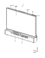
図1は、電子機器1の正面側からの斜視図であり、図2は、電子機器1の背面側からの斜視図である。なお、以下の各図では、便宜上、互いに直交する三方向が定義されている。X方向は、電子機器1の奥行方向(前後方向)に沿い、Y方向は、電子機器1の幅方向(左右方向、長手方向)に沿い、Z方向は、電子機器1の高さ方向(上下方向)に沿う。また、以下の説明では、X方向は前方、X方向の反対方向は後方とも称され、Y方向は左方、Y方向の反対方向は右方とも称され、Z方向は上方、Z方向の反対方向は下方とも称される。 FIG. 1 is a perspective view of the electronic device 1 from the front side, and FIG. 2 is a perspective view of the electronic device 1 from the back side. In the following drawings, three directions orthogonal to each other are defined for convenience. The X direction is along the depth direction (front-back direction) of the electronic device 1, the Y direction is along the width direction (left and right direction, longitudinal direction) of the electronic device 1, and the Z direction is the height direction (up and down) of the electronic device 1. Direction). In the following description, the X direction is also referred to as the front, the direction opposite to the X direction is also referred to as the rear, the Y direction is also referred to as the left, the direction opposite to the Y direction is also referred to as the right, the Z direction is upward, and the Z direction is opposite. The direction is also referred to as downward.
図1,2に示されるように、電子機器1は、例えば、オールインワン(AIO)タイプのデスクトップ型のパーソナルコンピュータとして構成されており、ベース筐体2と、ディスプレイ筐体3と、を備えている。ディスプレイ筐体3には、ディスプレイユニット6や基板7(図3参照)が収容され、ベース筐体2には、ODD(Optical Disk Drive)装置8や、スピーカユニット(不図示)等が収容されている。ディスプレイ筐体3は、筐体の一例である。なお、電子機器1は、この例には限定されず、例えば、クラムシェル型(ノートブック型)のパーソナルコンピュータや、映像表示装置、テレビジョン受像機、ゲーム機、映像表示制御装置、情報記憶装置等であってもよい。
As shown in FIGS. 1 and 2, the electronic device 1 is configured as, for example, an all-in-one (AIO) type desktop personal computer, and includes a
図1,2に示されるように、ディスプレイ筐体3は、ベース筐体2に支持されている。ディスプレイ筐体3は、例えば、ディスプレイユニット6の表示画面6aが露出する前壁3aと、表示画面6aとは反対側に位置された後壁3bと、前壁3aと後壁3bとに亘った周壁3cと、を有している。ディスプレイユニット6は、表示画面6aが前方(X方向)から視認可能な状態に、ディスプレイ筐体3に支持されている。ディスプレイ筐体3とベース筐体2とは、不図示のケーブル等の配線部材を介して、互いに電気的に接続されている。
As shown in FIGS. 1 and 2, the display housing 3 is supported by the
図2に示されるように、後壁3bには、凹部3dが設けられている。凹部3dは、X方向に凹みX方向と反対方向に向けて開口している。また、後壁3bには、凹部3dの底を形成する底壁3eが設けられている。すなわち、底壁3eは、凹部3dに面している。底壁3eは、X方向と直交する方向(YZ平面)に沿って延びている。底壁3eには、複数の開口部3fa,3fb,3fcが設けられている。開口部3fa,3fb,3fcは、それぞれ、貫通孔であり、底壁3eの厚さ方向に底壁3eを貫通している。複数の開口部3fa,3fb,3fcは、互いに間隔を空けてY方向に並べられている。底壁3eは、第1壁の一例であり、開口部3fa,3fb,3fcは、第1開口部の一例である。
As shown in FIG. 2, the
図1,2に示されるように、ディスプレイ筐体3は、フロントカバー9とリヤカバー10とを含む複数の部材の組み合わせによって構成されている。フロントカバー9は、前壁3aおよび周壁3cの一部を含む。リヤカバー10は、後壁3bおよび周壁3cの一部を含む。フロントカバー9とリヤカバー10とは、爪やネジ等によって互いに結合されている。
As shown in FIGS. 1 and 2, the display housing 3 is configured by a combination of a plurality of members including a
図3は、実施形態の電子機器1の背面側からの例示的な斜視図であって、リヤカバー10が取り外された状態の図である。図3に示されるように、基板7は、フロントカバー9に固定されている。基板7の後面には、複数のコネクタ11や、冷却装置21、CPU(Central Processing Unit)等の複数の電子部品が実装されている。基板7内の配線とこれら複数の電子部品とによって、電子機器1の制御回路の少なくとも一部が構成されている。
FIG. 3 is an exemplary perspective view from the rear side of the electronic device 1 according to the embodiment, in a state where the
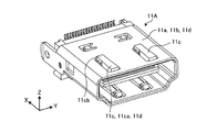
図4は、実施形態の基板7の背面側からの例示的な斜視図である。図4に示されるように、複数のコネクタ11は、基板7の裏面に実装されて、ディスプレイ筐体3に収容されている。複数のコネクタ11は、互いに間隔を空けてY方向に並べられている。複数のコネクタ11は、基板7から突出する所謂ストレートタイプである。具体的には、複数のコネクタ11は、それぞれ、基板7から底壁3e(図2参照)に向けて突出している。各コネクタ11は、それぞれ、雌型であり、各コネクタ11には、雄型の外部コネクタ(不図示)が挿入される。
FIG. 4 is an exemplary perspective view from the back side of the
複数のコネクタ11は、複数のコネクタ11Aと、複数のコネクタ11Bと、一つのコネクタ11Cと、を含む。コネクタ11Aとコネクタ11Bとは、互いに種類が異なる。コネクタ11Aは、例えばHDMI(登録商標)(High Definition Multimedia Interface)コネクタであり、コネクタ11Bは、例えばUSB(Universal Serial Bus)コネクタであり、コネクタ11Cは、例えばLAN(Local Area Network)コネクタである。なお、コネクタ11の数や種類は、上記以外であってもよい。
The plurality of
図5は、実施形態のコネクタ11の背面かつ上面側からの例示的な斜視図である。図6は、実施形態のコネクタ11の背面かつ下面側からの例示的な斜視図である。図5,6のコネクタ11は、具体的にはコネクタ11Aである。
FIG. 5 is an exemplary perspective view from the rear and top side of the
図5,6に示されるように、コネクタ11Aは、シェル11aを有している。シェル11aは、X方向に沿って延びた筒状に形成され、ディスプレイ筐体3における底壁3eの外部に向かって開口している。シェル11aは、例えばX方向から見た場合に略矩形に形成されている。シェル11aは、上下に扁平に形成されている。シェル11a内に外部コネクタが挿入される。
As shown in FIGS. 5 and 6, the
シェル11aは、筒部11bと、筒部11bに接続された複数のバネ11cと、を有している。筒部11bとバネ11cとは、それぞれ、シェル11aの外周部11dの一部を構成している。バネ11cは、X方向に延びている。バネ11cは、筒部11bと接続された基端部11caと、基端部11caとは反対側の先端部11cbと有している。基端部11caと先端部11cbとは、互いにX方向に離れている。先端部11cbは、先端部11cbと接触した外部コネクタをシェル11aの内側へ向けて押す。これにより、外部コネクタがシェル11aに保持される。シェル11aは、保持部とも称される。
The
図4に示されるように、コネクタ11Bは、コネクタ11Aと同様に、シェル11aを有している。但し、コネクタ11Bのシェル11aは、左右に扁平に形成されている。また、コネクタ11Cは、コネクタ11Aと同様に、シェル11aを有している。但し、コネクタ11Cのシェル11aは、上下の高さと左右の幅が略同じに形成されている。また、コネクタ11Cでは、バネ11cは、筒部11bの先端部に設けられている。
As shown in FIG. 4, the connector 11B has a
コネクタ11Aは、ディスプレイ筐体3における底壁3eの開口部3fa(図2参照)からディスプレイ筐体3の外部に露出している。コネクタ11Bは、底壁3eの開口部3fb(図2参照)からディスプレイ筐体3の外部に露出している。コネクタ11Cは、底壁3eの開口部3fc(図2参照)からディスプレイ筐体3の外部に露出している。
The
図7は、実施形態の電子機器1のコネクタ11を含む部分の例示的なXZ断面図である。図7のコネクタ11は、具体的にはコネクタ11Aである。図7に示されるように、ディスプレイ筐体3内には、第1導電部材12と、第2導電部材14とが設けられている。
FIG. 7 is an exemplary XZ sectional view of a portion including the
第1導電部材12は、金属材料によって構成され、導電性を有している。第1導電部材12は、折り曲げが施された板金部材によって構成されている。第1導電部材12は、ディスプレイ筐体3の後壁3bにおける少なくとも底壁3eの内側に位置されている。第1導電部材12は、底壁3eに沿った壁12aを有している。壁12aは、第2壁の一例である。
The first conductive member 12 is made of a metal material and has conductivity. The first conductive member 12 is configured by a bent sheet metal member. The first conductive member 12 is located at least inside the
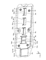
図8は、実施形態の後壁3bおよび第1導電部材12の正面かつ下面側からの例示的な斜視図である。図8に示されるように、第1導電部材12の壁12aには、開口部12ba、12bb,12bcが設けられている。開口部12ba、12bb,12bcは、それぞれ、貫通孔であり、壁12aの厚さ方向に壁12aを貫通している。開口部12ba、12bb,12bcは、それぞれ、底壁3eの開口部3fa,3fb,3fcと底壁3eの厚さ方向(X方向)に面し、開口部3fa,3fb,3fcと通じている。換言すると、開口部12ba、12bb,12bcと、開口部3fa,3fb,3fcとは、底壁3eの厚さ方向に並べられている。開口部12ba、12bb,12bcは、第2開口部の一例である。
FIG. 8 is an exemplary perspective view of the
また、第1導電部材12は、壁12aと接続された延部12ca,12cb,12ccを有している。延部12ca,12cb,12ccは、それぞれ、板状に形成されている。延部12ca,12cb,12ccは、壁12aの開口部12ba、12bb,12bc毎に設けられている。一つの開口部12baに対して一つの延部12caが設けられ、一つの開口部12bbに対して二つの延部12cbが設けられ、一つの開口部12bcに対して一つの延部12ccが設けられている。 The first conductive member 12 has extending portions 12ca, 12cb, and 12cc connected to the wall 12a. Each of the extending portions 12ca, 12cb, and 12cc is formed in a plate shape. The extensions 12ca, 12cb, 12cc are provided for each of the openings 12ba, 12bb, 12bc of the wall 12a. One extension 12ca is provided for one opening 12ba, two extensions 12cb are provided for one opening 12bb, and one extension 12cc is provided for one opening 12bc. ing.
延部12ca,12cb,12ccは、それぞれ、壁12aにおける開口部12ba、12bb,12bcの周囲から、底壁3eに向かってすなわちX方向の反対方向に延びている。具体的には、延部12caは、壁12aにおける開口部12baのZ方向側の部分からX方向の反対方向に延びるとともに、Y方向に延びている。二つの延部12cbは、壁12aにおける開口部12bbのZ方向側の部分および壁12aにおける開口部12bbのZ方向の反対方向側の部分からX方向の反対方向に延びるとともに、Y方向に延びている。延部12ccは、壁12aにおける開口部12bcのY方向の反対方向側の部分からX方向の反対方向に延びるとともに、Z方向に延びている。延部12ca,12cb,12ccは、それぞれ、折曲部とも称される。
The extensions 12ca, 12cb, and 12cc extend from the periphery of the openings 12ba, 12bb, and 12bc in the wall 12a toward the
図7に示されるように、開口部12ba、12bb,12bcには、コネクタ11のシェル11aが入れられている。なお、図7では、開口部12ba、12bb,12bcのうち開口部12baだけが示されている。シェル11aは、ディスプレイ筐体3の外部に向かって開口し開口部3fa,3fb,3fcから露出している。
As shown in FIG. 7, a
図8に示されるように、第1導電部材12は、壁12aの厚さ方向に壁12aを貫通した複数の位置決め突起13によって、YZ平面に沿う方向の位置決めがされている。第1導電部材12は、ネジ等の結合具によって後壁3bに固定されている。
As shown in FIG. 8, the first conductive member 12 is positioned in a direction along the YZ plane by a plurality of positioning
図9は、実施形態の後壁3b、第1導電部材12、および第2導電部材14の正面かつ下面側からの例示的な斜視図である。図7,9に示されるように第2導電部材14は、第1導電部材12と重ねられた状態で、第1導電部材12に固定されている。
FIG. 9 is an exemplary perspective view of the
第2導電部材14は、板状に形成され、導電性およびクッション性(弾性)を有している。第2導電部材14は、例えば、弾性部材と弾性部材を覆った導電部材との組み合わせによって構成されてもよいし、導電性フィラー入りのエラストマによって構成されてもよい。上記の弾性部材は、例えば合成樹脂材料やエラストマによって構成され、導電部材は、金属材料によって構成されうる。 The second conductive member 14 is formed in a plate shape and has conductivity and cushioning property (elasticity). The second conductive member 14 may be formed of, for example, a combination of an elastic member and a conductive member covering the elastic member, or may be formed of an elastomer containing a conductive filler. The elastic member may be made of, for example, a synthetic resin material or an elastomer, and the conductive member may be made of a metal material.
第2導電部材14は、第1部分14aと、第1部分14aと接続された第2部分14ca,14cb,14ccと、を有している。 The second conductive member 14 has a first portion 14a and second portions 14ca, 14cb, 14cc connected to the first portion 14a.
第1部分14aは、X方向と直交する方向(YZ平面)に延びた板状に形成されている。第1部分14aは、第1導電部材12の壁12aに対して後壁3bの底壁3eとは反対側にて壁12aに重ねられた状態で、壁12aに固定されている。
The first portion 14a is formed in a plate shape extending in a direction (YZ plane) orthogonal to the X direction. The first portion 14a is fixed to the wall 12a in a state where the first portion 14a overlaps the wall 12a on the side opposite to the
第2導電部材14には、複数の開口部14ba,14bbが設けられている。複数の開口部14ba,14bbは、それぞれ、貫通孔であり、第1部分14aの厚さ方向に第1部分14aを貫通している。開口部14ba,14bbは、それぞれ、第1導電部材12の開口部12ba、12bbと、底壁3eの開口部3fa,3fbと、底壁3eの厚さ方向(X方向)に面し、開口部12ba、12bbおよび開口部3fa,3fbと通じている。換言すると、開口部14ba,14bbと、第1導電部材12の開口部12ba、12bbと、底壁3eの開口部3fa,3fbとは、底壁3eの厚さ方向(X方向)に並べられている。
The second conductive member 14 has a plurality of openings 14ba, 14bb. The plurality of openings 14ba, 14bb are through holes, respectively, and penetrate the first portion 14a in the thickness direction of the first portion 14a. The openings 14ba, 14bb face the openings 12ba, 12bb of the first conductive member 12, the openings 3fa, 3fb of the
第2部分14ca,14cb,14ccは、それぞれ、板状に形成されている。第2部分14ca,14cb,14ccは、それぞれ、第1部分14aに対して折り曲げられ(図9参照)、第1部分14aから底壁3eに向かってすなわちX方向の反対方向に延び、コネクタ11の外周部11dに沿っている。なお、図9では、折り曲げがされていない状態の第2部分14ca,14cb,14ccが示されている。
The second portions 14ca, 14cb, and 14cc are each formed in a plate shape. Each of the second portions 14ca, 14cb, and 14cc is bent with respect to the first portion 14a (see FIG. 9), and extends from the first portion 14a toward the
第2部分14ca,14cb,14ccは、第1導電部材12の延部12ca,12cb,12cc毎に設けられて、延部12ca,12cb,12ccに重ねられている。 The second portions 14ca, 14cb, and 14cc are provided for each of the extending portions 12ca, 12cb, and 12cc of the first conductive member 12, and overlap the extending portions 12ca, 12cb, and 12cc.
第2部分14ca,14cbは、それぞれ、第1部分14aにおける開口部14ba,14bbの周囲から、底壁3eに向かってすなわちX方向の反対方向に延びている。具体的には、第2部分14caは、第1部分14aにおける開口部14baのZ方向側の部分からX方向の反対方向に延びるとともに、Y方向に延びている。二つの第2部分14cbは、第1部分14aにおける開口部14bbのZ方向側の部分および第1部分14aにおける開口部14bbのZ方向の反対方向側の部分からX方向の反対方向に延びるとともに、Y方向に延びている。第2部分14ccは、第1部分14aにおけるY方向の端部からX方向の反対方向に延びるとともに、Z方向に延びている。第2部分14ca,14cb,14ccは、それぞれ、折曲部とも称される。
The second portions 14ca, 14cb extend from the periphery of the openings 14ba, 14bb in the first portion 14a toward the
次に、第2部分14ca,14cb,14ccと、コネクタ11との接続について、第2部分14caを代表として詳しく説明する。図7に示されるように、第2部分14caは、第1部分14aから底壁3eへ向かって延びて開口部12baに入れられ、コネクタ11Aにおけるシェル11aの外周部11dと接触している。第2部分14caは、延部12caと外周部11dとの間に介在している。詳しくは、第2部分14caは、延部12caと外周部11dと挟まれて、圧縮している。また、第2部分14caは、コネクタ11Aにおけるバネ11cの先端部11cbから離間して当該バネ11cの基端部11caと接触している。
Next, connection between the second portions 14ca, 14cb, and 14cc and the
図10は、実施形態の電子機器1の製造工程を示す図であって、第2導電部材14の第2部分14caが折り曲げられる前の状態を示す図である。詳しくは、図10は、リヤカバー10とフロントカバー9(図10では不図示)とが結合される前の状態であって、基板7と後壁3bとの間の距離が組立状態よりも大きい状態が示されている。この状態から、リヤカバー10とフロントカバー9とが、X方向に近接されて組付けられる過程で、コネクタ11Aが第2導電部材14の第2部分14caを押し曲げる。これにより、第2部分14caが、第1導電部材12の延部12caとコネクタ11Aの外周部11dと挟まれて、圧縮する。
FIG. 10 is a diagram illustrating a manufacturing process of the electronic device 1 according to the embodiment, and is a diagram illustrating a state before the second portion 14ca of the second conductive member 14 is bent. More specifically, FIG. 10 shows a state before the
第2部分14cbは、第1導電部材12の延部12cbとコネクタ11Bの外周部11dとの間に介在している。また、第2部分14ccは、第1導電部材12の延部12ccとコネクタ11Cの外周部11dとの間に介在している。第2部分14ccは、コネクタ11Cのバネ11cから離間している。
The second portion 14cb is interposed between the extending portion 12cb of the first conductive member 12 and the outer
上記構造においては、各コネクタ11のシェル11aは、第1導電部材12の第2部分14cbおよび第1部分14aを介して第1導電部材12に電気的に接続されている。よって、例えば、コネクタ11への外部コネクタの接続の際等に、シェル11aに外部から静電気が伝達された場合には、当該静電気が、第2導電部材14を介して、第1導電部材12ひいてはディスプレイ筐体3に伝達される。よって、シェル11aから基板7への静電気の伝達が抑制される。
In the above structure, the
以上のように、本実形態では、第2導電部材14は、壁12a(第2壁)に対して底壁3e(第1壁)とは反対側にて壁12aに重ねられた第1部分14aと、第1部分14aから底壁3eへ向かって延びて開口部12ba、12bb,12bc(第2開口部)に入れられシェル11aの外周部11dと接触した第2部分14ca,14cb,14ccと、を有している。
As described above, in the present embodiment, the second conductive member 14 is configured such that the first portion overlapped with the wall 12a on the side opposite to the
このような構成によれば、例えば、シェル11aに外部から静電気が伝達された場合には、当該静電気が第2導電部材14を介して第1導電部材12に伝達される。よって、コネクタ11から基板7への静電気の伝達が抑制されやすい。
According to such a configuration, for example, when static electricity is transmitted to the
また、本実施形態では、第1導電部材12は、壁12aにおける開口部12ba、12bb,12bcの周囲から底壁3eに向かって延びた延部12ca,12cb,12ccを有している。延部12ca,12cb,12ccと外周部11dとの間に第2部分14ca,14cb,14ccが介在している。
In the present embodiment, the first conductive member 12 has extending portions 12ca, 12cb, 12cc extending from the periphery of the openings 12ba, 12bb, 12bc in the wall 12a toward the
このような構成によれば、例えば、第2部分14ca,14cb,14ccと第1導電部材12との接触面積を大きくしやすいので、静電気が第2導電部材14を介して第1導電部材12により伝達される。 According to such a configuration, for example, it is easy to increase the contact area between the second portions 14ca, 14cb, 14cc and the first conductive member 12, so that static electricity is generated by the first conductive member 12 via the second conductive member 14. Is transmitted.
また、本実施形態では、複数のコネクタ11が設けられ、第2導電部材14は、コネクタ11毎に設けられた複数の第2部分14ca,14cb,14ccを有している。
In this embodiment, a plurality of
このような構成によれば、例えば、複数のコネクタ11に対する第2導電部材14の位置決めが容易である。また、第2導電部材14は一つ設ければよいので、電子機器1の部品点数の増大化が抑制されやすい。
According to such a configuration, for example, the positioning of the second conductive member 14 with respect to the plurality of
また、本実施形態では、シェル11aは、外周部11dの一部を構成する筒部11bと、筒部11bと接続された基端部11caと基端部11caとは反対側の先端部11cbと有し外周部11dの一部を構成するバネ11cと、を有している。第2部分14ca,14cbは、先端部11cbから離間して基端部11caと接触している。
Further, in the present embodiment, the
このような構成によれば、例えば、シェル11aと接触する第2導電部材14がバネ11cの動きを阻害するのが抑制される。
According to such a configuration, for example, the second conductive member 14 in contact with the
また、図11に示されるように、第2導電部材14は、バネ11c(具体的には、バネ11cの先端部11cb)から離間して、シェル11aの外周部11dのうち先端部11cb側に接触している第2部分14cdを有していてもよい。具体的には、第2部分14cdは、バネ11cから離間して、シェル11aの外周部11dの先端部に接触している。第2部分14cdは、例えば、開口部14baに対して第2部分14caの反対側に設けられている。
As shown in FIG. 11, the second conductive member 14 is separated from the
このような構成によれば、例えば、シェル11aと接触する第2導電部材14がバネ11cの動きを阻害するのが抑制される。
According to such a configuration, for example, the second conductive member 14 in contact with the
以上、本発明の実施形態が例示されたが、上記実施形態は一例であって、発明の範囲を限定することは意図していない。上記実施形態は、その他の様々な形態で実施されることが可能であり、発明の要旨を逸脱しない範囲で、種々の省略、置き換え、組み合わせ、変更を行うことができる。また、各構成や、形状、等のスペック(構造や、種類、方向、形式、大きさ、長さ、幅、厚さ、高さ、数、配置、位置、材質等)は、適宜に変更して実施することができる。 As described above, the embodiment of the present invention has been exemplified, but the above embodiment is an example, and is not intended to limit the scope of the invention. The above embodiments can be implemented in other various forms, and various omissions, replacements, combinations, and changes can be made without departing from the spirit of the invention. In addition, the specifications (structure, type, direction, type, size, length, width, thickness, height, number, arrangement, position, material, etc.) of each configuration, shape, etc. may be changed as appropriate. Can be implemented.
1…電子機器、3…ディスプレイ筐体(筐体)、3e…底壁(第1壁)、3fa,3fb,3fc…開口部(第1開口部)、7…基板、11,11A,11B,11C…コネクタ、11a…シェル、11b…筒部、11c…バネ、11ca…基端部、11cb…先端部、11d…外周部、12…第1導電部材、12a…壁(第2壁)、12ba,12bb,12bc…開口部(第2開口部)、12ca,12cb,12cc…延部、14…第2導電部材、14a…第1部分、14ca,14cb,14cc,14cd…第2部分。 DESCRIPTION OF SYMBOLS 1 ... Electronic device, 3 ... Display housing (housing), 3e ... Bottom wall (1st wall), 3fa, 3fb, 3fc ... Opening (1st opening), 7 ... Substrate, 11, 11A, 11B, 11C connector, 11a shell, 11b cylindrical part, 11c spring, 11ca base end, 11cb distal end, 11d outer peripheral part, 12 first conductive member, 12a wall (second wall), 12ba , 12bb, 12bc ... opening (second opening), 12ca, 12cb, 12cc ... extension, 14 ... second conductive member, 14a ... first part, 14ca, 14cb, 14cc, 14cd ... second part.
Claims (5)
前記筐体における前記第1壁の内側に位置され、前記第1壁に沿った第2壁を有し、前記第2壁に前記第1開口部と前記厚さ方向に面した第2開口部が形成された第1導電部材と、
前記筐体に収容された基板と、
前記基板に実装されて前記筐体に収容され、前記第2開口部に入れられ前記筐体の外部に向かって開口し前記第1開口部から露出した筒状のシェルを有したコネクタと、
前記第2壁に対して前記第1壁とは反対側にて前記第2壁に重ねられた第1部分と、前記第1部分から前記第1壁へ向かって延びて前記第2開口部に入れられ前記シェルの外周部と接触した第2部分と、を有した第2導電部材と、
を備えた電子機器。 A housing having a first wall and a first opening provided through the first wall in a thickness direction of the first wall;
A second opening that is located inside the first wall in the housing and extends along the first wall, the second opening facing the first opening and the thickness direction on the second wall; A first conductive member formed with
A substrate housed in the housing,
A connector mounted on the board and housed in the housing, having a cylindrical shell placed in the second opening, opening toward the outside of the housing, and exposed from the first opening;
A first portion overlapped with the second wall on a side opposite to the first wall with respect to the second wall; and a second portion extending from the first portion toward the first wall. A second conductive member having a second portion inserted therein and in contact with an outer peripheral portion of the shell;
Electronic equipment with.
前記延部と前記外周部との間に前記第2部分が介在した、請求項1に記載の電子機器。 The first conductive member has an extension extending from the periphery of the second opening in the second wall toward the first wall,
The electronic device according to claim 1, wherein the second portion is interposed between the extending portion and the outer peripheral portion.
前記第1壁には、複数の前記第1開口部が形成され、
前記第2壁には、複数の前記第2開口部が形成され、
前記第2導電部材は、複数の前記第2部分を有した、請求項1または2に記載の電子機器。 Comprising a plurality of said connectors,
A plurality of the first openings are formed in the first wall;
A plurality of the second openings are formed in the second wall;
The electronic device according to claim 1, wherein the second conductive member has a plurality of the second portions.
前記第2部分は、前記先端部から離間して前記基端部と接触した、請求項1〜3のうちいずれか一つに記載の電子機器。 The shell has a cylindrical portion that forms a part of the outer peripheral portion, a base end connected to the cylindrical portion, and a distal end opposite to the base end, and forms a part of the outer peripheral portion. Having a spring,
4. The electronic device according to claim 1, wherein the second portion is separated from the distal end portion and is in contact with the base end portion. 5.
前記第2部分は、前記バネから離間して、前記シェルの前記先端部側に接触した、請求項1〜3のうちいずれか一つに記載の電子機器。 The shell has a tubular portion that forms at least a part of the outer peripheral portion, a spring having a proximal end connected to the tubular portion and a distal end opposite to the proximal end,
4. The electronic device according to claim 1, wherein the second portion is separated from the spring and is in contact with the distal end side of the shell. 5.
Priority Applications (1)
| Application Number | Priority Date | Filing Date | Title |
|---|---|---|---|
| JP2018184707A JP6624263B1 (en) | 2018-09-28 | 2018-09-28 | Electronics |
Applications Claiming Priority (1)
| Application Number | Priority Date | Filing Date | Title |
|---|---|---|---|
| JP2018184707A JP6624263B1 (en) | 2018-09-28 | 2018-09-28 | Electronics |
Publications (2)
| Publication Number | Publication Date |
|---|---|
| JP6624263B1 JP6624263B1 (en) | 2019-12-25 |
| JP2020052971A true JP2020052971A (en) | 2020-04-02 |
Family
ID=69100910
Family Applications (1)
| Application Number | Title | Priority Date | Filing Date |
|---|---|---|---|
| JP2018184707A Active JP6624263B1 (en) | 2018-09-28 | 2018-09-28 | Electronics |
Country Status (1)
| Country | Link |
|---|---|
| JP (1) | JP6624263B1 (en) |
Cited By (1)
| Publication number | Priority date | Publication date | Assignee | Title |
|---|---|---|---|---|
| WO2021193012A1 (en) | 2020-03-24 | 2021-09-30 | 日本トムソン株式会社 | Follower bearing |
Citations (4)
| Publication number | Priority date | Publication date | Assignee | Title |
|---|---|---|---|---|
| JPH08305464A (en) * | 1995-04-28 | 1996-11-22 | Toshiba Corp | External extended device for portable electronic equipment |
| JP2007165274A (en) * | 2005-12-16 | 2007-06-28 | Avermedia Technologies Inc | Adapter device provided with elastic power conduction means |
| WO2010116449A1 (en) * | 2009-03-30 | 2010-10-14 | 富士通株式会社 | Electronic device having connector |
| JP2015530724A (en) * | 2012-10-04 | 2015-10-15 | タイコ・エレクトロニクス・コーポレイションTyco Electronics Corporation | Header assembly |
-
2018
- 2018-09-28 JP JP2018184707A patent/JP6624263B1/en active Active
Patent Citations (4)
| Publication number | Priority date | Publication date | Assignee | Title |
|---|---|---|---|---|
| JPH08305464A (en) * | 1995-04-28 | 1996-11-22 | Toshiba Corp | External extended device for portable electronic equipment |
| JP2007165274A (en) * | 2005-12-16 | 2007-06-28 | Avermedia Technologies Inc | Adapter device provided with elastic power conduction means |
| WO2010116449A1 (en) * | 2009-03-30 | 2010-10-14 | 富士通株式会社 | Electronic device having connector |
| JP2015530724A (en) * | 2012-10-04 | 2015-10-15 | タイコ・エレクトロニクス・コーポレイションTyco Electronics Corporation | Header assembly |
Cited By (1)
| Publication number | Priority date | Publication date | Assignee | Title |
|---|---|---|---|---|
| WO2021193012A1 (en) | 2020-03-24 | 2021-09-30 | 日本トムソン株式会社 | Follower bearing |
Also Published As
| Publication number | Publication date |
|---|---|
| JP6624263B1 (en) | 2019-12-25 |
Similar Documents
| Publication | Publication Date | Title |
|---|---|---|
| US9923310B2 (en) | Electrical receptacle connector | |
| TWI586049B (en) | Electrical plug connector with shielding and grounding features | |
| US9502839B2 (en) | Electrical receptacle connector | |
| TWI593194B (en) | Electrical receptacle connector with shielding and grounding features | |
| US7361059B2 (en) | Electrical connector | |
| TWM544721U (en) | Electric socket connector | |
| JP6226304B2 (en) | Electronics | |
| CN109256647A (en) | Electric connector for socket | |
| TWM537740U (en) | Vertical electrical socket connector | |
| TWM456012U (en) | Connector structure | |
| US20130221812A1 (en) | Television | |
| TWM467231U (en) | Electric connection member, portable electronic machine and electric connector | |
| TWM544715U (en) | Electric socket connector | |
| JP6624263B1 (en) | Electronics | |
| JP6362212B2 (en) | Connector, mating connector and connector assembly | |
| KR200497887Y1 (en) | Input assembly | |
| JP2013125624A (en) | Connector | |
| US20130164983A1 (en) | Connector and electronic device having same | |
| JP2007087910A (en) | Electric connector | |
| JP2021166158A (en) | Electronic device | |
| JP6674121B1 (en) | Electronics | |
| JP3201237U (en) | Connector structure | |
| TWI583084B (en) | Power connector | |
| TW201509034A (en) | HDMI connector | |
| JP6734557B1 (en) | Electronics |
Legal Events
| Date | Code | Title | Description |
|---|---|---|---|
| A621 | Written request for application examination |
Free format text: JAPANESE INTERMEDIATE CODE: A621 Effective date: 20181126 |
|
| TRDD | Decision of grant or rejection written | ||
| A01 | Written decision to grant a patent or to grant a registration (utility model) |
Free format text: JAPANESE INTERMEDIATE CODE: A01 Effective date: 20191029 |
|
| A61 | First payment of annual fees (during grant procedure) |
Free format text: JAPANESE INTERMEDIATE CODE: A61 Effective date: 20191111 |
|
| R150 | Certificate of patent or registration of utility model |
Ref document number: 6624263 Country of ref document: JP Free format text: JAPANESE INTERMEDIATE CODE: R150 |
|
| R250 | Receipt of annual fees |
Free format text: JAPANESE INTERMEDIATE CODE: R250 |