JP2020005405A - Switching power supply device - Google Patents
Switching power supply device Download PDFInfo
- Publication number
- JP2020005405A JP2020005405A JP2018122801A JP2018122801A JP2020005405A JP 2020005405 A JP2020005405 A JP 2020005405A JP 2018122801 A JP2018122801 A JP 2018122801A JP 2018122801 A JP2018122801 A JP 2018122801A JP 2020005405 A JP2020005405 A JP 2020005405A
- Authority
- JP
- Japan
- Prior art keywords
- voltage
- output voltage
- transistor
- output
- circuit
- Prior art date
- Legal status (The legal status is an assumption and is not a legal conclusion. Google has not performed a legal analysis and makes no representation as to the accuracy of the status listed.)
- Granted
Links
Images
Abstract
Description
本発明は、フィードバック回路を備えたスイッチング電源装置に関する。 The present invention relates to a switching power supply device provided with a feedback circuit.
フィードバック回路を備えたスイッチング電源装置としては、例えば、特許文献1に記載のものが知られている。特許文献1に記載のスイッチング電源装置において、フィードバック回路は、二次側の出力電圧の多寡に関するフィードバック信号を一次側の制御回路に出力する。制御回路は、出力電圧が一定になるように一次側のFETをフィードバック制御する。
As a switching power supply device provided with a feedback circuit, for example, a switching power supply device described in
従来のスイッチング電源装置は、フィードバック制御の応答が遅いため、出力電流が急激に変化した場合、出力電圧が大きく変動(跳ね上がったり、跳ね下がったり)してしまう。その結果、スイッチング電源装置の出力端子に接続される負荷(装置)のIC等の許容電圧範囲を超えてしまい、負荷(装置)が誤動作するおそれがある。 Since the conventional switching power supply device has a slow response in the feedback control, when the output current changes rapidly, the output voltage greatly fluctuates (bounces up or down). As a result, the load (device) connected to the output terminal of the switching power supply may exceed the allowable voltage range of the IC or the like, and the load (device) may malfunction.
本発明は上記事情に鑑みてなされたものであって、その課題とするところは、出力電圧の変動を抑制可能なスイッチング電源装置を提供することにある。 The present invention has been made in view of the above circumstances, and an object of the present invention is to provide a switching power supply device capable of suppressing a change in output voltage.
上記課題を解決するために、本発明に係るスイッチング電源装置は、
トランスと、
前記トランスの一次側にスイッチング電圧を供給するスイッチ手段と、
前記スイッチ手段を制御する制御回路と、
前記トランスの二次側の誘起電圧を直流化して出力電圧を生成する第1出力部と、
前記出力電圧を検出して前記制御回路にフィードバック信号を出力するフィードバック回路と、
を備えるスイッチング電源装置であって、
前記出力電圧よりも電圧値の高い補助電圧を生成する第2出力部と、
前記出力電圧と所定の上限基準電圧および下限基準電圧とを比較する比較回路と、
前記出力電圧が前記上限基準電圧よりも大きい場合に、前記出力電圧を低下させる放電回路と、
前記出力電圧が前記下限基準電圧よりも小さい場合に、前記補助電圧を利用して前記出力電圧を上昇させる充電回路と、を備えることを特徴とする。
In order to solve the above problems, a switching power supply according to the present invention is
With a transformer,
Switch means for supplying a switching voltage to a primary side of the transformer,
A control circuit for controlling the switch means;
A first output unit for converting an induced voltage on the secondary side of the transformer into a direct current to generate an output voltage;
A feedback circuit that detects the output voltage and outputs a feedback signal to the control circuit;
A switching power supply device comprising:
A second output unit that generates an auxiliary voltage having a higher voltage value than the output voltage;
A comparison circuit that compares the output voltage with a predetermined upper reference voltage and a lower reference voltage;
A discharge circuit that reduces the output voltage when the output voltage is higher than the upper-limit reference voltage;
A charging circuit configured to increase the output voltage by using the auxiliary voltage when the output voltage is lower than the lower-limit reference voltage.
この構成では、出力電流が急激に低下して出力電圧が上昇した場合、放電回路が出力電圧を低下させる一方、出力電流が急激に上昇して出力電圧が低下した場合、充電回路が補助電圧を利用して出力電圧を上昇させる。したがって、この構成によれば、急激な出力電流変化に伴う出力電圧の変動を抑制することができる。 With this configuration, when the output current drops sharply and the output voltage rises, the discharging circuit drops the output voltage, while when the output current rises sharply and the output voltage drops, the charging circuit drops the auxiliary voltage. Use to increase the output voltage. Therefore, according to this configuration, it is possible to suppress a change in the output voltage due to a sudden change in the output current.
上記スイッチング電源装置において、
前記放電回路は、第1トランジスタを含み、
前記第1トランジスタの電流路の一端は前記出力電圧が印加される第1電圧ラインに接続され、前記第1トランジスタの前記電流路の他端はグランドに接続され、
前記比較回路は、前記出力電圧が前記上限基準電圧よりも大きい場合に、前記第1トランジスタをオン状態にするよう構成できる。
In the above switching power supply,
The discharge circuit includes a first transistor,
One end of a current path of the first transistor is connected to a first voltage line to which the output voltage is applied, the other end of the current path of the first transistor is connected to ground,
The comparison circuit may be configured to turn on the first transistor when the output voltage is higher than the upper limit reference voltage.
上記スイッチング電源装置において、
前記充電回路は、第2トランジスタを含み、
前記第2トランジスタの電流路の一端は前記補助電圧が印加される第2電圧ラインに接続され、前記第2トランジスタの前記電流路の他端は前記第1電圧ラインに接続され、
前記比較回路は、前記出力電圧が前記下限基準電圧よりも小さい場合に、前記第2トランジスタをオン状態にするよう構成できる。
In the above switching power supply,
The charging circuit includes a second transistor,
One end of a current path of the second transistor is connected to a second voltage line to which the auxiliary voltage is applied, and the other end of the current path of the second transistor is connected to the first voltage line;
The comparison circuit may be configured to turn on the second transistor when the output voltage is lower than the lower reference voltage.
上記スイッチング電源装置において、
前記第1トランジスタは、NチャネルMOSFETからなり、
前記NチャネルMOSFETのドレイン端子は、放電用抵抗を介して前記第1電圧ラインに接続され、
前記第2トランジスタは、PチャネルMOSFETからなり、
前記PチャネルMOSFETのドレイン端子は、充電用抵抗を介して前記第1電圧ラインに接続されるよう構成できる。
In the above switching power supply,
The first transistor includes an N-channel MOSFET,
A drain terminal of the N-channel MOSFET is connected to the first voltage line via a discharge resistor;
The second transistor comprises a P-channel MOSFET;
The drain terminal of the P-channel MOSFET may be configured to be connected to the first voltage line via a charging resistor.
上記スイッチング電源装置において、
前記比較回路は、
前記上限基準電圧および前記下限基準電圧を生成するシャントレギュレータおよび分圧抵抗回路と、
前記上限基準電圧と前記出力電圧とを比較する第1コンパレータと、
前記下限基準電圧と前記出力電圧とを比較する第2コンパレータと、を含むよう構成できる。
In the above switching power supply,
The comparison circuit includes:
A shunt regulator and a voltage dividing resistor circuit for generating the upper reference voltage and the lower reference voltage,
A first comparator that compares the upper limit reference voltage with the output voltage;
A second comparator for comparing the lower limit reference voltage with the output voltage.
本発明によれば、出力電圧の変動を抑制可能なスイッチング電源装置を提供することができる。 ADVANTAGE OF THE INVENTION According to this invention, the switching power supply device which can suppress the fluctuation | variation of an output voltage can be provided.
以下、添付図面を参照して、本発明に係るスイッチング電源装置の実施形態について説明する。 Hereinafter, an embodiment of a switching power supply according to the present invention will be described with reference to the accompanying drawings.
[スイッチング電源装置の構成]
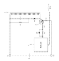
図1および図2に、本発明の一実施形態に係るスイッチング電源装置を示す。本実施形態に係るスイッチング電源装置は、トランス1と、トランス1の一次側に設けられた一次側回路と、トランス1の二次側に設けられた二次側回路と、を備える。
[Configuration of Switching Power Supply]
1 and 2 show a switching power supply according to an embodiment of the present invention. The switching power supply according to the present embodiment includes a
一次側回路は、図1に示すように、スイッチ手段2と、スイッチ手段2を制御する制御回路3と、直流電源Eに接続される入力端子T1,T2と、を含む。さらに、一次側回路は、トランス1の一次側巻線の一端および他端間に接続されたスナバ回路(抵抗R1、コンデンサC1、ダイオードD1)と、スイッチ手段2の制御端子に接続された回路(抵抗R2、抵抗R3、ダイオードD2)と、を含む。
As shown in FIG. 1, the primary side circuit includes a switch unit 2, a control circuit 3 for controlling the switch unit 2, and input terminals T1 and T2 connected to the DC power supply E. Further, the primary circuit includes a snubber circuit (resistor R1, capacitor C1, and diode D1) connected between one end and the other end of the primary winding of the
スイッチ手段2は、例えばトランジスタ(本実施形態では、NチャネルMOSFET)からなる。スイッチ手段2は、制御回路3の制御下でスイッチング動作を行い、直流電源Eから供給される直流電圧をスイッチングして、トランス1の一次側にスイッチング電圧を供給する。スイッチ手段2の電流路の一端(ドレイン端子)は、トランス1の一次側巻線の他端に接続され、スイッチ手段2の電流路の他端(ソース端子)は、抵抗R4を介して入力端子T2に接続される。
The switch means 2 is composed of, for example, a transistor (in this embodiment, an N-channel MOSFET). The switching means 2 performs a switching operation under the control of the control circuit 3 to switch the DC voltage supplied from the DC power supply E and supply the switching voltage to the primary side of the
制御回路3は、例えば、マイコンおよび/または専用のICからなる。制御回路3は、出力電圧が一定になるように、フィードバック信号を受けてスイッチ手段2を制御(例えば、PWM制御)する。 The control circuit 3 includes, for example, a microcomputer and / or a dedicated IC. The control circuit 3 receives the feedback signal and controls the switch unit 2 (for example, PWM control) so that the output voltage becomes constant.
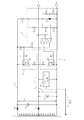
二次側回路は、図2に示すように、第1出力部(ダイオードD3、コンデンサC2)と、第2出力部(ダイオードD4、コンデンサC3)と、フィードバック回路4と、放電回路5と、充電回路6と、比較回路7と、負荷(例えば、ICを備えた装置)が接続される出力端子T3,T4と、を含む。
As shown in FIG. 2, the secondary circuit includes a first output unit (diode D3, capacitor C2), a second output unit (diode D4, capacitor C3), a feedback circuit 4, a
第1出力部は、ダイオードD3およびコンデンサC2を含み、トランス1の二次側の誘起電圧を直流化して出力電圧Voを生成する。トランス1の二次側巻線には、二次側巻線の一端と他端との間に少なくとも1つのタップが設けられている。ダイオードD3は、アノードが上記タップに接続され、カソードが出力端子T3に接続される。コンデンサC2は、一端がダイオードD3のカソードに接続され、他端が出力端子(グランド端子)T4に接続される。ダイオードD3のカソードと出力端子T3とを接続し、出力電圧Voが印加される電圧ラインを、第1電圧ラインL1とする。
The first output unit includes a diode D3 and a capacitor C2, and converts the induced voltage on the secondary side of the
第2出力部は、ダイオードD4およびコンデンサC3を含み、トランス1の二次側の誘起電圧を直流化して出力電圧Voよりも電圧値の高い補助電圧Vo’を生成する。ダイオードD4は、アノードがトランス1の二次側巻線の一端に接続され、カソードが充電回路6を介して出力端子T3に接続される。コンデンサC3は、一端がダイオードD4のカソードに接続され、他端が出力端子(グランド端子)T4に接続される。ダイオードD4のカソードと抵抗R9および抵抗R10の一端とを接続し、補助電圧Vo’が印加される電圧ラインを、第2電圧ラインL2とする。
The second output unit includes a diode D4 and a capacitor C3, converts the induced voltage on the secondary side of the
フィードバック回路4は、出力端子T3,T4間に接続される。フィードバック回路4は、出力電圧Voを検出して制御回路3にフィードバック信号を出力する。フィードバック回路4は、例えば、シャントレギュレータおよびフォトカプラ等で構成される。 The feedback circuit 4 is connected between the output terminals T3 and T4. The feedback circuit 4 detects the output voltage Vo and outputs a feedback signal to the control circuit 3. The feedback circuit 4 includes, for example, a shunt regulator and a photocoupler.
放電回路5は、第1トランジスタQAと、放電用抵抗R5と、抵抗R6とを含む。第1トランジスタQAは、例えば、NチャネルMOSFETからなる。第1トランジスタQAの電流路の一端(ドレイン端子D)は、放電用抵抗R5を介して第1電圧ラインL1に接続される。第1トランジスタQAの電流路の他端(ソース端子S)は、出力端子(グランド端子)T4に接続される。第1トランジスタQAの制御端子(ゲート端子G)は、抵抗R6を介して比較回路7に接続される。
The
充電回路6は、第2トランジスタQBと、充電用抵抗R7と、抵抗R8とを含む。第2トランジスタQBは、例えば、PチャネルMOSFETからなる。第2トランジスタQBの電流路の一端(ソース端子S)は、第2電圧ラインL2に接続される。第2トランジスタQBの電流路の他端(ドレイン端子D)は、充電用抵抗R7を介して第1電圧ラインL1に接続される。第2トランジスタQBの制御端子(ゲート端子G)は、抵抗R8を介して比較回路7および抵抗R9の他端に接続される。 Charging circuit 6 includes a second transistor QB, a charging resistor R7, and a resistor R8. The second transistor QB is formed of, for example, a P-channel MOSFET. One end (source terminal S) of the current path of the second transistor QB is connected to the second voltage line L2. The other end (drain terminal D) of the current path of the second transistor QB is connected to the first voltage line L1 via the charging resistor R7. The control terminal (gate terminal G) of the second transistor QB is connected to the other end of the comparison circuit 7 and the other end of the resistor R9 via the resistor R8.
比較回路7は、シャントレギュレータIC1と、第1コンパレータIC2と、第2コンパレータIC3と、抵抗R11〜R16とを含む。比較回路7は、出力電圧Voと所定の上限基準電圧VoHおよび下限基準電圧VoLとを比較する。 The comparison circuit 7 includes a shunt regulator IC1, a first comparator IC2, a second comparator IC3, and resistors R11 to R16. The comparison circuit 7 compares the output voltage Vo with predetermined upper and lower reference voltages VoH and VoL.
上限基準電圧VoHおよび下限基準電圧VoLは、シャントレギュレータIC1および抵抗R11〜R15により生成される。シャントレギュレータIC1は、アノード端子、カソード端子およびリファレンス端子を有する。アノード端子は出力端子(グランド端子)T4に接続され、カソード端子は抵抗R10を介して第2電圧ラインL2に接続される。アノード端子−カソード端子間には、抵抗R11,R12を直列接続した第1分圧抵抗回路と、抵抗R13〜R15を直列接続した第2分圧抵抗回路(本発明の「分圧抵抗回路」に相当)とが接続される。リファレンス端子は、抵抗R11,R12の分圧点に接続される。なお、抵抗R11,R12は、ツェナーダイオード等の定電圧生成用の素子に置き換えることができる。 The upper reference voltage VoH and the lower reference voltage VoL are generated by the shunt regulator IC1 and the resistors R11 to R15. The shunt regulator IC1 has an anode terminal, a cathode terminal, and a reference terminal. The anode terminal is connected to the output terminal (ground terminal) T4, and the cathode terminal is connected to the second voltage line L2 via the resistor R10. Between the anode terminal and the cathode terminal, a first voltage-dividing resistor circuit in which resistors R11 and R12 are connected in series, and a second voltage-dividing resistor circuit in which resistors R13 to R15 are connected in series (in the "voltage-dividing resistor circuit" of the present invention). ) Is connected. The reference terminal is connected to a voltage dividing point of the resistors R11 and R12. Note that the resistors R11 and R12 can be replaced with a constant voltage generating element such as a Zener diode.
第2分圧抵抗回路では、抵抗R13,R14の分圧点における電圧が上限基準電圧VoHに相当し、抵抗R14,R15の分圧点における電圧が下限基準電圧VoLに相当する。一例として、出力電圧Voが5.00Vの場合、上限基準電圧VoHを5.25Vに設定し、下限基準電圧VoLを4.75Vに設定することができる。 In the second voltage dividing resistor circuit, the voltage at the voltage dividing point of the resistors R13 and R14 corresponds to the upper limit reference voltage VoH, and the voltage at the voltage dividing point of the resistors R14 and R15 corresponds to the lower limit reference voltage VoL. For example, when the output voltage Vo is 5.00 V, the upper limit reference voltage VoH can be set to 5.25 V, and the lower limit reference voltage VoL can be set to 4.75 V.
第1コンパレータIC2は、反転入力端子、非反転入力端子および出力端子を有する。反転入力端子は抵抗R13,R14の分圧点に接続され、非反転入力端子は第1電圧ラインL1に接続され、出力端子は抵抗R6を介して第1トランジスタQAの制御端子(ゲート端子G)に接続される。 The first comparator IC2 has an inverting input terminal, a non-inverting input terminal, and an output terminal. The inverting input terminal is connected to the voltage dividing point of the resistors R13 and R14, the non-inverting input terminal is connected to the first voltage line L1, and the output terminal is a control terminal (gate terminal G) of the first transistor QA via the resistor R6. Connected to.
第1コンパレータIC2は、出力電圧Voと上限基準電圧VoHとを比較し、出力電圧Voが上限基準電圧VoHよりも大きい場合にハイレベルの信号を出力して、第1トランジスタQAをオン状態にする。第1トランジスタQAをオン状態になると、出力電圧Voに関係するコンデンサC2の電荷が、放電用抵抗R5を介して出力端子(グランド端子)T4に放電される。その結果、出力電圧Voの上昇が抑制され、出力電圧Voが低下する。 The first comparator IC2 compares the output voltage Vo with the upper limit reference voltage VoH, and outputs a high-level signal when the output voltage Vo is higher than the upper limit reference voltage VoH to turn on the first transistor QA. . When the first transistor QA is turned on, the charge of the capacitor C2 related to the output voltage Vo is discharged to the output terminal (ground terminal) T4 via the discharging resistor R5. As a result, an increase in the output voltage Vo is suppressed, and the output voltage Vo decreases.
第2コンパレータIC3は、反転入力端子、非反転入力端子および出力端子を有する。反転入力端子は第1電圧ラインL1に接続され、非反転入力端子は抵抗R14,R15の分圧点に接続され、出力端子は抵抗R16および抵抗R8を介して第2トランジスタQBの制御端子(ゲート端子G)に接続される。 The second comparator IC3 has an inverting input terminal, a non-inverting input terminal, and an output terminal. The inverting input terminal is connected to the first voltage line L1, the non-inverting input terminal is connected to the voltage dividing point of the resistors R14 and R15, and the output terminal is the control terminal (gate) of the second transistor QB via the resistors R16 and R8. Terminal G).
第2コンパレータIC3は、出力電圧Voと下限基準電圧VoLとを比較し、出力電圧Voが下限基準電圧VoLよりも小さい場合にローレベルの信号を出力して、第2トランジスタQBをオン状態にする。第2トランジスタQBをオン状態になると、充電用抵抗R7を介して補助電圧Vo’が第1電圧ラインL1に印加され、コンデンサC2が充電される。その結果、出力電圧Voの低下が抑制され、出力電圧Voが上昇する。 The second comparator IC3 compares the output voltage Vo with the lower-limit reference voltage VoL, outputs a low-level signal when the output voltage Vo is lower than the lower-limit reference voltage VoL, and turns on the second transistor QB. . When the second transistor QB is turned on, the auxiliary voltage Vo 'is applied to the first voltage line L1 via the charging resistor R7, and the capacitor C2 is charged. As a result, a decrease in the output voltage Vo is suppressed, and the output voltage Vo increases.
[出力電流が急激に低下したときのスイッチング電源装置の動作]
次に、本実施形態に係るスイッチング電源装置の動作について説明する。以下では、定常状態における出力電圧Voを5.00V、上限基準電圧VoHを5.25V、下限基準電圧VoLを4.75Vとする。
[Operation of switching power supply device when output current drops sharply]
Next, the operation of the switching power supply according to the present embodiment will be described. Hereinafter, it is assumed that the output voltage Vo in the steady state is 5.00 V, the upper limit reference voltage VoH is 5.25 V, and the lower limit reference voltage VoL is 4.75 V.
出力電流が急激に低下した場合、出力電圧Voは5.00Vから上昇し始める。出力電圧Voが上限基準電圧VoHよりも大きくなると、第1コンパレータIC2はハイレベルの信号を出力する。第1コンパレータIC2のハイレベルの信号は、抵抗R6を介して第1トランジスタQAのゲート端子Gに印加される。第1トランジスタQAは、ゲート−ソース間電圧VGSがゲート閾値電圧Vth以上になり、オン状態に移行する。 When the output current drops sharply, the output voltage Vo starts to increase from 5.00V. When the output voltage Vo becomes higher than the upper limit reference voltage VoH, the first comparator IC2 outputs a high-level signal. The high-level signal of the first comparator IC2 is applied to the gate terminal G of the first transistor QA via the resistor R6. In the first transistor QA, the gate-source voltage V GS becomes higher than or equal to the gate threshold voltage Vth , and the first transistor QA shifts to the ON state.
第1トランジスタQAがオン状態になると、出力電圧Voに関係するコンデンサC2の電荷が、放電用抵抗R5を介して出力端子(グランド端子)T4に放電される。その結果、出力電圧Voの上昇が抑制され、出力電圧Voが低下する。 When the first transistor QA is turned on, the charge of the capacitor C2 related to the output voltage Vo is discharged to the output terminal (ground terminal) T4 via the discharging resistor R5. As a result, an increase in the output voltage Vo is suppressed, and the output voltage Vo decreases.
出力電圧Voが上限基準電圧VoHよりも小さくなると、第1コンパレータIC2はローレベルの信号を出力する。第1トランジスタQAは、ゲート−ソース間電圧VGSがゲート閾値電圧Vthよりも小さくなり、オフ状態に移行する。第1トランジスタQAがオフ状態になると放電回路5による放電が停止し、出力電圧Voは定常状態に戻る。
When the output voltage Vo becomes lower than the upper limit reference voltage VoH, the first comparator IC2 outputs a low-level signal. In the first transistor QA, the gate-source voltage V GS becomes lower than the gate threshold voltage Vth , and the first transistor QA shifts to the off state. When the first transistor QA is turned off, the discharge by the
[出力電流が急激に上昇したときのスイッチング電源装置の動作]
一方、出力電流が急激に上昇した場合、出力電圧Voは5.00Vから低下し始める。出力電圧Voが下限基準電圧VoLよりも小さくなると、第2コンパレータIC3はローレベルの信号を出力する。第2コンパレータIC3のローレベルの信号は、抵抗R16および抵抗R8を介して第2トランジスタQBのゲート端子Gに印加される。第2トランジスタQBは、ゲート電圧が下がり、ゲート−ソース間電圧VGSがゲート閾値電圧Vth以上になるので、オン状態に移行する。
[Operation of switching power supply device when output current sharply increases]
On the other hand, when the output current sharply increases, the output voltage Vo starts to decrease from 5.00V. When the output voltage Vo becomes lower than the lower-limit reference voltage VoL, the second comparator IC3 outputs a low-level signal. The low-level signal of the second comparator IC3 is applied to the gate terminal G of the second transistor QB via the resistors R16 and R8. The gate voltage of the second transistor QB drops, and the gate-source voltage V GS becomes equal to or higher than the gate threshold voltage Vth , so that the second transistor QB shifts to the ON state.
第2トランジスタQBがオン状態になると、充電用抵抗R7を介して補助電圧Vo’が第1電圧ラインL1に印加され、コンデンサC2が充電される。その結果、出力電圧Voの低下が抑制され、出力電圧Voが上昇する。 When the second transistor QB is turned on, the auxiliary voltage Vo 'is applied to the first voltage line L1 via the charging resistor R7, and the capacitor C2 is charged. As a result, a decrease in the output voltage Vo is suppressed, and the output voltage Vo increases.
出力電圧Voが下限基準電圧VoLよりも大きくなると、第2トランジスタQBはハイレベルの信号を出力する。第2トランジスタQBは、ゲート電圧が上がり、ゲート−ソース間電圧VGSがゲート閾値電圧Vthよりも小さくなり、オフ状態に移行する。第2トランジスタQBオフ状態になると充電回路6による充電が停止し、出力電圧Voは定常状態に戻る。 When the output voltage Vo becomes higher than the lower limit reference voltage VoL, the second transistor QB outputs a high-level signal. The gate voltage of the second transistor QB rises, the gate-source voltage V GS becomes lower than the gate threshold voltage Vth , and the second transistor QB shifts to the off state. When the second transistor QB is turned off, charging by the charging circuit 6 stops, and the output voltage Vo returns to a steady state.
上記のとおり、本実施形態に係るスイッチング電源装置では、出力電流が急激に低下した場合、放電回路5が出力電圧Voの上昇を抑制するとともに出力電圧Voを素早く低下させる一方、出力電流が急激に上昇した場合、充電回路6が補助電圧Vo’を利用して出力電圧Voの低下を抑制するとともに出力電圧Voを素早く上昇させる。したがって、本実施形態に係るスイッチング電源装置によれば、急激な出力電流変化に伴う出力電圧Voの変動を抑制することができる。
As described above, in the switching power supply device according to the present embodiment, when the output current sharply decreases, the
以上、本発明に係るスイッチング電源装置の実施形態について説明したが、本発明は上記実施形態に限定されるものではない。 The embodiments of the switching power supply device according to the present invention have been described above, but the present invention is not limited to the above embodiments.
本発明の放電回路は、出力電圧Voが上限基準電圧VoHよりも大きい場合に出力電圧Voを低下させるのであれば、適宜構成を変更できる。また、本発明の充電回路は、出力電圧Voが下限基準電圧VoLよりも小さい場合に補助電圧Vo’を利用して出力電圧Voを上昇させるのであれば、適宜構成を変更できる。 The configuration of the discharge circuit of the present invention can be changed as appropriate as long as the output voltage Vo is reduced when the output voltage Vo is higher than the upper limit reference voltage VoH. In addition, the configuration of the charging circuit of the present invention can be appropriately changed as long as the output voltage Vo is increased using the auxiliary voltage Vo 'when the output voltage Vo is lower than the lower limit reference voltage VoL.
本発明の比較回路は、出力電圧Voと上限基準電圧VoHおよび下限基準電圧VoLとを比較して、出力電圧Voが上限基準電圧VoHよりも大きい場合に放電回路による放電を実行させ、出力電圧Voが下限基準電圧VoLよりも小さい場合に充電回路による充電を実行させるのであれば、適宜構成を変更できる。 The comparison circuit of the present invention compares the output voltage Vo with the upper-limit reference voltage VoH and the lower-limit reference voltage VoL, and when the output voltage Vo is higher than the upper-limit reference voltage VoH, causes the discharge circuit to execute the discharge. If the charging is performed by the charging circuit when is smaller than the lower limit reference voltage VoL, the configuration can be changed as appropriate.
上記実施形態の比較回路7は、上限基準電圧VoHおよび下限基準電圧VoLをシャントレギュレータIC1および抵抗R11〜R15により生成することで外部信号を不要としているが、外部信号を利用するのであれば、上記構成を省略してもよい。 The comparison circuit 7 of the above embodiment eliminates the need for an external signal by generating the upper reference voltage VoH and the lower reference voltage VoL by the shunt regulator IC1 and the resistors R11 to R15. The configuration may be omitted.
本発明の第2出力部は、出力電圧Voよりも電圧値の高い補助電圧Vo’を生成するのであれば、適宜構成を変更できる。 The configuration of the second output unit of the present invention can be appropriately changed as long as it generates the auxiliary voltage Vo 'having a higher voltage value than the output voltage Vo.
1 トランス
2 スイッチ手段
3 制御回路
4 フィードバック回路
5 放電回路
6 充電回路
7 比較回路
DESCRIPTION OF
Claims (5)
前記トランスの一次側にスイッチング電圧を供給するスイッチ手段と、
前記スイッチ手段を制御する制御回路と、
前記トランスの二次側の誘起電圧を直流化して出力電圧を生成する第1出力部と、
前記出力電圧を検出して前記制御回路にフィードバック信号を出力するフィードバック回路と、
を備えるスイッチング電源装置であって、
前記出力電圧よりも電圧値の高い補助電圧を生成する第2出力部と、
前記出力電圧と所定の上限基準電圧および下限基準電圧とを比較する比較回路と、
前記出力電圧が前記上限基準電圧よりも大きい場合に、前記出力電圧を低下させる放電回路と、
前記出力電圧が前記下限基準電圧よりも小さい場合に、前記補助電圧を利用して前記出力電圧を上昇させる充電回路と、を備える
ことを特徴とするスイッチング電源装置。 With a transformer,
Switch means for supplying a switching voltage to a primary side of the transformer,
A control circuit for controlling the switch means;
A first output unit for converting an induced voltage on the secondary side of the transformer into a direct current to generate an output voltage;
A feedback circuit that detects the output voltage and outputs a feedback signal to the control circuit;
A switching power supply device comprising:
A second output unit that generates an auxiliary voltage having a higher voltage value than the output voltage;
A comparison circuit that compares the output voltage with a predetermined upper reference voltage and a lower reference voltage;
A discharge circuit that reduces the output voltage when the output voltage is higher than the upper-limit reference voltage;
A switching power supply device comprising: a charging circuit that increases the output voltage by using the auxiliary voltage when the output voltage is lower than the lower reference voltage.
前記第1トランジスタの電流路の一端は前記出力電圧が印加される第1電圧ラインに接続され、前記第1トランジスタの前記電流路の他端はグランドに接続され、
前記比較回路は、前記出力電圧が前記上限基準電圧よりも大きい場合に、前記第1トランジスタをオン状態にする
ことを特徴とする請求項1に記載のスイッチング電源装置。 The discharge circuit includes a first transistor,
One end of a current path of the first transistor is connected to a first voltage line to which the output voltage is applied, the other end of the current path of the first transistor is connected to ground,
The switching power supply device according to claim 1, wherein the comparison circuit turns on the first transistor when the output voltage is higher than the upper limit reference voltage.
前記第2トランジスタの電流路の一端は前記補助電圧が印加される第2電圧ラインに接続され、前記第2トランジスタの前記電流路の他端は前記第1電圧ラインに接続され、
前記比較回路は、前記出力電圧が前記下限基準電圧よりも小さい場合に、前記第2トランジスタをオン状態にする
ことを特徴とする請求項2に記載のスイッチング電源装置。 The charging circuit includes a second transistor,
One end of a current path of the second transistor is connected to a second voltage line to which the auxiliary voltage is applied, and the other end of the current path of the second transistor is connected to the first voltage line;
The switching power supply device according to claim 2, wherein the comparison circuit turns on the second transistor when the output voltage is lower than the lower reference voltage.
前記NチャネルMOSFETのドレイン端子は、放電用抵抗を介して前記第1電圧ラインに接続され、
前記第2トランジスタは、PチャネルMOSFETからなり、
前記PチャネルMOSFETのドレイン端子は、充電用抵抗を介して前記第1電圧ラインに接続される
ことを特徴とする請求項3に記載のスイッチング電源装置。 The first transistor includes an N-channel MOSFET,
A drain terminal of the N-channel MOSFET is connected to the first voltage line via a discharge resistor;
The second transistor comprises a P-channel MOSFET;
The switching power supply according to claim 3, wherein a drain terminal of the P-channel MOSFET is connected to the first voltage line via a charging resistor.
前記上限基準電圧および前記下限基準電圧を生成するシャントレギュレータおよび分圧抵抗回路と、
前記上限基準電圧と前記出力電圧とを比較する第1コンパレータと、
前記下限基準電圧と前記出力電圧とを比較する第2コンパレータと、を含む
ことを特徴とする請求項1〜4のいずれか一項に記載のスイッチング電源装置。 The comparison circuit includes:
A shunt regulator and a voltage dividing resistor circuit for generating the upper reference voltage and the lower reference voltage,
A first comparator that compares the upper limit reference voltage with the output voltage;
The switching power supply device according to claim 1, further comprising: a second comparator that compares the lower reference voltage with the output voltage.
Priority Applications (1)
| Application Number | Priority Date | Filing Date | Title |
|---|---|---|---|
| JP2018122801A JP6975689B2 (en) | 2018-06-28 | 2018-06-28 | Switching power supply |
Applications Claiming Priority (1)
| Application Number | Priority Date | Filing Date | Title |
|---|---|---|---|
| JP2018122801A JP6975689B2 (en) | 2018-06-28 | 2018-06-28 | Switching power supply |
Publications (2)
| Publication Number | Publication Date |
|---|---|
| JP2020005405A true JP2020005405A (en) | 2020-01-09 |
| JP6975689B2 JP6975689B2 (en) | 2021-12-01 |
Family
ID=69100812
Family Applications (1)
| Application Number | Title | Priority Date | Filing Date |
|---|---|---|---|
| JP2018122801A Active JP6975689B2 (en) | 2018-06-28 | 2018-06-28 | Switching power supply |
Country Status (1)
| Country | Link |
|---|---|
| JP (1) | JP6975689B2 (en) |
Citations (7)
| Publication number | Priority date | Publication date | Assignee | Title |
|---|---|---|---|---|
| JPH09212247A (en) * | 1996-01-30 | 1997-08-15 | Nec Corp | Referrence voltage generation circuit |
| JP2001258249A (en) * | 2000-03-14 | 2001-09-21 | Matsushita Electric Ind Co Ltd | Dc-dc converter |
| US6385058B1 (en) * | 2001-05-17 | 2002-05-07 | Northrop Grumman | Active bleed voltage balancing circuit |
| JP2010119257A (en) * | 2008-11-14 | 2010-05-27 | Toyota Motor Corp | Power supply device and vehicle |
| JP2015073407A (en) * | 2013-10-04 | 2015-04-16 | 株式会社デンソー | Insulating power supply device |
| JP2015139321A (en) * | 2014-01-23 | 2015-07-30 | ニチコン株式会社 | Reference voltage output circuit and power supply device |
| JP2016116261A (en) * | 2014-12-11 | 2016-06-23 | 株式会社デンソー | Switching power supply circuit |
-
2018
- 2018-06-28 JP JP2018122801A patent/JP6975689B2/en active Active
Patent Citations (7)
| Publication number | Priority date | Publication date | Assignee | Title |
|---|---|---|---|---|
| JPH09212247A (en) * | 1996-01-30 | 1997-08-15 | Nec Corp | Referrence voltage generation circuit |
| JP2001258249A (en) * | 2000-03-14 | 2001-09-21 | Matsushita Electric Ind Co Ltd | Dc-dc converter |
| US6385058B1 (en) * | 2001-05-17 | 2002-05-07 | Northrop Grumman | Active bleed voltage balancing circuit |
| JP2010119257A (en) * | 2008-11-14 | 2010-05-27 | Toyota Motor Corp | Power supply device and vehicle |
| JP2015073407A (en) * | 2013-10-04 | 2015-04-16 | 株式会社デンソー | Insulating power supply device |
| JP2015139321A (en) * | 2014-01-23 | 2015-07-30 | ニチコン株式会社 | Reference voltage output circuit and power supply device |
| JP2016116261A (en) * | 2014-12-11 | 2016-06-23 | 株式会社デンソー | Switching power supply circuit |
Also Published As
| Publication number | Publication date |
|---|---|
| JP6975689B2 (en) | 2021-12-01 |
Similar Documents
| Publication | Publication Date | Title |
|---|---|---|
| TWI396375B (en) | Switching power supply and related control method | |
| US7492615B2 (en) | Switching power supply | |
| US7636246B2 (en) | Start-up time reduction in switching regulators | |
| US7518836B2 (en) | Switching mode power supply and method for performing protection operation thereof | |
| US9647561B2 (en) | Programmable current limit circuit for a programmable power supply | |
| KR101091923B1 (en) | Switching mode power supply and method for producing bias voltage thereof | |
| US7388763B2 (en) | Switching power supply | |
| US9252674B2 (en) | Transistor gate driver with charge pump circuit for offline power converters | |
| US20070291516A1 (en) | Switching power supply for reducing external parts for overcurrent protection | |
| US8089791B2 (en) | Compensation circuit and compensation method for current mode power converters | |
| US7800927B2 (en) | Method and circuit for providing compensations of current mode power converters | |
| US10090767B2 (en) | Switching power supply device having a pulse width holder | |
| US20140043002A1 (en) | Control circuit with deep burst mode for power converter | |
| JP2017127109A (en) | Switching power supply device | |
| KR101489962B1 (en) | Power converter, switching control device thereof and driving method thereof | |
| JP2008011636A (en) | Switching power supply | |
| US10396674B2 (en) | Flyback power converter circuit and primary side controller circuit thereof | |
| US20200382005A1 (en) | Method for driving a switch in a power converter, drive circuit and power converter | |
| US10468981B2 (en) | Switching power supply device | |
| WO2020202760A1 (en) | Switching control circuit, power supply circuit | |
| JP2019080433A (en) | Synchronous rectification circuit and switching power unit | |
| US20230143191A1 (en) | Integrated circuit and power supply circuit | |
| JP2020005405A (en) | Switching power supply device | |
| KR101011083B1 (en) | Switching mode power supply having primary bios power supply | |
| JP2014112996A (en) | Light load detection circuit, switching regulator, and method of controlling the same |
Legal Events
| Date | Code | Title | Description |
|---|---|---|---|
| A621 | Written request for application examination |
Free format text: JAPANESE INTERMEDIATE CODE: A621 Effective date: 20201210 |
|
| A977 | Report on retrieval |
Free format text: JAPANESE INTERMEDIATE CODE: A971007 Effective date: 20211027 |
|
| TRDD | Decision of grant or rejection written | ||
| A01 | Written decision to grant a patent or to grant a registration (utility model) |
Free format text: JAPANESE INTERMEDIATE CODE: A01 Effective date: 20211104 |
|
| A61 | First payment of annual fees (during grant procedure) |
Free format text: JAPANESE INTERMEDIATE CODE: A61 Effective date: 20211108 |
|
| R150 | Certificate of patent or registration of utility model |
Ref document number: 6975689 Country of ref document: JP Free format text: JAPANESE INTERMEDIATE CODE: R150 |