JP2020005367A - Power conversion device - Google Patents
Power conversion device Download PDFInfo
- Publication number
- JP2020005367A JP2020005367A JP2018120984A JP2018120984A JP2020005367A JP 2020005367 A JP2020005367 A JP 2020005367A JP 2018120984 A JP2018120984 A JP 2018120984A JP 2018120984 A JP2018120984 A JP 2018120984A JP 2020005367 A JP2020005367 A JP 2020005367A
- Authority
- JP
- Japan
- Prior art keywords
- magnetic
- current sensor
- sensor element
- shield plate
- power converter
- Prior art date
- Legal status (The legal status is an assumption and is not a legal conclusion. Google has not performed a legal analysis and makes no representation as to the accuracy of the status listed.)
- Granted
Links
- 238000006243 chemical reaction Methods 0.000 title claims abstract description 25
- 230000004907 flux Effects 0.000 claims abstract description 85
- 239000002184 metal Substances 0.000 claims description 14
- 229910052751 metal Inorganic materials 0.000 claims description 14
- 238000004804 winding Methods 0.000 claims description 10
- 239000000696 magnetic material Substances 0.000 claims description 7
- 239000004065 semiconductor Substances 0.000 description 38
- HEZMWWAKWCSUCB-PHDIDXHHSA-N (3R,4R)-3,4-dihydroxycyclohexa-1,5-diene-1-carboxylic acid Chemical compound O[C@@H]1C=CC(C(O)=O)=C[C@H]1O HEZMWWAKWCSUCB-PHDIDXHHSA-N 0.000 description 10
- 239000003990 capacitor Substances 0.000 description 9
- 238000001514 detection method Methods 0.000 description 9
- 238000004088 simulation Methods 0.000 description 7
- 230000000694 effects Effects 0.000 description 6
- 239000000463 material Substances 0.000 description 5
- 230000035945 sensitivity Effects 0.000 description 5
- XEEYBQQBJWHFJM-UHFFFAOYSA-N Iron Chemical compound [Fe] XEEYBQQBJWHFJM-UHFFFAOYSA-N 0.000 description 4
- 230000008859 change Effects 0.000 description 3
- 238000010586 diagram Methods 0.000 description 3
- 230000035699 permeability Effects 0.000 description 3
- 238000005259 measurement Methods 0.000 description 2
- 230000001629 suppression Effects 0.000 description 2
- RYGMFSIKBFXOCR-UHFFFAOYSA-N Copper Chemical compound [Cu] RYGMFSIKBFXOCR-UHFFFAOYSA-N 0.000 description 1
- 229910000976 Electrical steel Inorganic materials 0.000 description 1
- 229910052782 aluminium Inorganic materials 0.000 description 1
- XAGFODPZIPBFFR-UHFFFAOYSA-N aluminium Chemical compound [Al] XAGFODPZIPBFFR-UHFFFAOYSA-N 0.000 description 1
- 239000004020 conductor Substances 0.000 description 1
- 229910052802 copper Inorganic materials 0.000 description 1
- 239000010949 copper Substances 0.000 description 1
- 230000008878 coupling Effects 0.000 description 1
- 238000010168 coupling process Methods 0.000 description 1
- 238000005859 coupling reaction Methods 0.000 description 1
- 239000000428 dust Substances 0.000 description 1
- 230000005669 field effect Effects 0.000 description 1
- 238000009499 grossing Methods 0.000 description 1
- 230000020169 heat generation Effects 0.000 description 1
- 229910052742 iron Inorganic materials 0.000 description 1
- 238000010030 laminating Methods 0.000 description 1
- 230000004048 modification Effects 0.000 description 1
- 238000012986 modification Methods 0.000 description 1
- 229910000889 permalloy Inorganic materials 0.000 description 1
- 230000009467 reduction Effects 0.000 description 1
- 229910001220 stainless steel Inorganic materials 0.000 description 1
- 239000010935 stainless steel Substances 0.000 description 1
Images


Classifications
-
- H—ELECTRICITY
- H02—GENERATION; CONVERSION OR DISTRIBUTION OF ELECTRIC POWER
- H02M—APPARATUS FOR CONVERSION BETWEEN AC AND AC, BETWEEN AC AND DC, OR BETWEEN DC AND DC, AND FOR USE WITH MAINS OR SIMILAR POWER SUPPLY SYSTEMS; CONVERSION OF DC OR AC INPUT POWER INTO SURGE OUTPUT POWER; CONTROL OR REGULATION THEREOF
- H02M7/00—Conversion of ac power input into dc power output; Conversion of dc power input into ac power output
- H02M7/003—Constructional details, e.g. physical layout, assembly, wiring or busbar connections
-
- G—PHYSICS
- G01—MEASURING; TESTING
- G01R—MEASURING ELECTRIC VARIABLES; MEASURING MAGNETIC VARIABLES
- G01R15/00—Details of measuring arrangements of the types provided for in groups G01R17/00 - G01R29/00, G01R33/00 - G01R33/26 or G01R35/00
- G01R15/14—Adaptations providing voltage or current isolation, e.g. for high-voltage or high-current networks
- G01R15/20—Adaptations providing voltage or current isolation, e.g. for high-voltage or high-current networks using galvano-magnetic devices, e.g. Hall-effect devices, i.e. measuring a magnetic field via the interaction between a current and a magnetic field, e.g. magneto resistive or Hall effect devices
- G01R15/207—Constructional details independent of the type of device used
-
- G—PHYSICS
- G01—MEASURING; TESTING
- G01R—MEASURING ELECTRIC VARIABLES; MEASURING MAGNETIC VARIABLES
- G01R19/00—Arrangements for measuring currents or voltages or for indicating presence or sign thereof
- G01R19/0092—Arrangements for measuring currents or voltages or for indicating presence or sign thereof measuring current only
-
- H—ELECTRICITY
- H02—GENERATION; CONVERSION OR DISTRIBUTION OF ELECTRIC POWER
- H02M—APPARATUS FOR CONVERSION BETWEEN AC AND AC, BETWEEN AC AND DC, OR BETWEEN DC AND DC, AND FOR USE WITH MAINS OR SIMILAR POWER SUPPLY SYSTEMS; CONVERSION OF DC OR AC INPUT POWER INTO SURGE OUTPUT POWER; CONTROL OR REGULATION THEREOF
- H02M1/00—Details of apparatus for conversion
- H02M1/0067—Converter structures employing plural converter units, other than for parallel operation of the units on a single load
- H02M1/007—Plural converter units in cascade
-
- H—ELECTRICITY
- H02—GENERATION; CONVERSION OR DISTRIBUTION OF ELECTRIC POWER
- H02M—APPARATUS FOR CONVERSION BETWEEN AC AND AC, BETWEEN AC AND DC, OR BETWEEN DC AND DC, AND FOR USE WITH MAINS OR SIMILAR POWER SUPPLY SYSTEMS; CONVERSION OF DC OR AC INPUT POWER INTO SURGE OUTPUT POWER; CONTROL OR REGULATION THEREOF
- H02M3/00—Conversion of dc power input into dc power output
- H02M3/003—Constructional details, e.g. physical layout, assembly, wiring or busbar connections
-
- H—ELECTRICITY
- H02—GENERATION; CONVERSION OR DISTRIBUTION OF ELECTRIC POWER
- H02M—APPARATUS FOR CONVERSION BETWEEN AC AND AC, BETWEEN AC AND DC, OR BETWEEN DC AND DC, AND FOR USE WITH MAINS OR SIMILAR POWER SUPPLY SYSTEMS; CONVERSION OF DC OR AC INPUT POWER INTO SURGE OUTPUT POWER; CONTROL OR REGULATION THEREOF
- H02M3/00—Conversion of dc power input into dc power output
- H02M3/02—Conversion of dc power input into dc power output without intermediate conversion into ac
- H02M3/04—Conversion of dc power input into dc power output without intermediate conversion into ac by static converters
- H02M3/10—Conversion of dc power input into dc power output without intermediate conversion into ac by static converters using discharge tubes with control electrode or semiconductor devices with control electrode
- H02M3/145—Conversion of dc power input into dc power output without intermediate conversion into ac by static converters using discharge tubes with control electrode or semiconductor devices with control electrode using devices of a triode or transistor type requiring continuous application of a control signal
- H02M3/155—Conversion of dc power input into dc power output without intermediate conversion into ac by static converters using discharge tubes with control electrode or semiconductor devices with control electrode using devices of a triode or transistor type requiring continuous application of a control signal using semiconductor devices only
- H02M3/156—Conversion of dc power input into dc power output without intermediate conversion into ac by static converters using discharge tubes with control electrode or semiconductor devices with control electrode using devices of a triode or transistor type requiring continuous application of a control signal using semiconductor devices only with automatic control of output voltage or current, e.g. switching regulators
- H02M3/158—Conversion of dc power input into dc power output without intermediate conversion into ac by static converters using discharge tubes with control electrode or semiconductor devices with control electrode using devices of a triode or transistor type requiring continuous application of a control signal using semiconductor devices only with automatic control of output voltage or current, e.g. switching regulators including plural semiconductor devices as final control devices for a single load
- H02M3/1584—Conversion of dc power input into dc power output without intermediate conversion into ac by static converters using discharge tubes with control electrode or semiconductor devices with control electrode using devices of a triode or transistor type requiring continuous application of a control signal using semiconductor devices only with automatic control of output voltage or current, e.g. switching regulators including plural semiconductor devices as final control devices for a single load with a plurality of power processing stages connected in parallel
- H02M3/1586—Conversion of dc power input into dc power output without intermediate conversion into ac by static converters using discharge tubes with control electrode or semiconductor devices with control electrode using devices of a triode or transistor type requiring continuous application of a control signal using semiconductor devices only with automatic control of output voltage or current, e.g. switching regulators including plural semiconductor devices as final control devices for a single load with a plurality of power processing stages connected in parallel switched with a phase shift, i.e. interleaved
-
- H—ELECTRICITY
- H02—GENERATION; CONVERSION OR DISTRIBUTION OF ELECTRIC POWER
- H02M—APPARATUS FOR CONVERSION BETWEEN AC AND AC, BETWEEN AC AND DC, OR BETWEEN DC AND DC, AND FOR USE WITH MAINS OR SIMILAR POWER SUPPLY SYSTEMS; CONVERSION OF DC OR AC INPUT POWER INTO SURGE OUTPUT POWER; CONTROL OR REGULATION THEREOF
- H02M7/00—Conversion of ac power input into dc power output; Conversion of dc power input into ac power output
- H02M7/42—Conversion of dc power input into ac power output without possibility of reversal
- H02M7/44—Conversion of dc power input into ac power output without possibility of reversal by static converters
- H02M7/48—Conversion of dc power input into ac power output without possibility of reversal by static converters using discharge tubes with control electrode or semiconductor devices with control electrode
- H02M7/53—Conversion of dc power input into ac power output without possibility of reversal by static converters using discharge tubes with control electrode or semiconductor devices with control electrode using devices of a triode or transistor type requiring continuous application of a control signal
- H02M7/537—Conversion of dc power input into ac power output without possibility of reversal by static converters using discharge tubes with control electrode or semiconductor devices with control electrode using devices of a triode or transistor type requiring continuous application of a control signal using semiconductor devices only, e.g. single switched pulse inverters
- H02M7/5387—Conversion of dc power input into ac power output without possibility of reversal by static converters using discharge tubes with control electrode or semiconductor devices with control electrode using devices of a triode or transistor type requiring continuous application of a control signal using semiconductor devices only, e.g. single switched pulse inverters in a bridge configuration
-
- H—ELECTRICITY
- H02—GENERATION; CONVERSION OR DISTRIBUTION OF ELECTRIC POWER
- H02M—APPARATUS FOR CONVERSION BETWEEN AC AND AC, BETWEEN AC AND DC, OR BETWEEN DC AND DC, AND FOR USE WITH MAINS OR SIMILAR POWER SUPPLY SYSTEMS; CONVERSION OF DC OR AC INPUT POWER INTO SURGE OUTPUT POWER; CONTROL OR REGULATION THEREOF
- H02M1/00—Details of apparatus for conversion
- H02M1/0003—Details of control, feedback or regulation circuits
- H02M1/0009—Devices or circuits for detecting current in a converter
-
- H—ELECTRICITY
- H02—GENERATION; CONVERSION OR DISTRIBUTION OF ELECTRIC POWER
- H02M—APPARATUS FOR CONVERSION BETWEEN AC AND AC, BETWEEN AC AND DC, OR BETWEEN DC AND DC, AND FOR USE WITH MAINS OR SIMILAR POWER SUPPLY SYSTEMS; CONVERSION OF DC OR AC INPUT POWER INTO SURGE OUTPUT POWER; CONTROL OR REGULATION THEREOF
- H02M1/00—Details of apparatus for conversion
- H02M1/0064—Magnetic structures combining different functions, e.g. storage, filtering or transformation
Abstract
Description
本発明は、電源から供給された電力の変換を、磁性部品を用いて行う電力変換装置に関する。 The present invention relates to a power converter that converts power supplied from a power supply using a magnetic component.
例えば、電気自動車、プラグインハイブリッドのような電動車両に搭載される大電力容量の電力変換装置では、バスバと、バスバに流れる電流量を検出するための電流センサとを備えることが多い。バスバとは、金属板もしくは金属棒で形成される導体部材であり、電流量が多い電流経路で用いられる。 For example, a large-capacity power converter mounted on an electric vehicle such as an electric vehicle or a plug-in hybrid often includes a bus bar and a current sensor for detecting an amount of current flowing through the bus bar. The bus bar is a conductor member formed of a metal plate or a metal rod, and is used in a current path having a large amount of current.
バスバに流れる電流は、磁束を発生させる。電流センサは、磁気検出素子を備え、その磁気検出素子がバスバに隣接させて配置される。バスバに流れる電流の値は、磁気検出素子が出力する磁束数に応じた信号値に対して、係数を乗じることで算出される。磁気検出素子は、以降「電流センサ素子」と表記する。 The current flowing through the bus bar generates a magnetic flux. The current sensor includes a magnetic detection element, and the magnetic detection element is arranged adjacent to the bus bar. The value of the current flowing through the bus bar is calculated by multiplying a signal value corresponding to the number of magnetic fluxes output from the magnetic detection element by a coefficient. The magnetic detection element is hereinafter referred to as “current sensor element”.
測定対象のバスバ以外に磁束を発生させる外乱磁場は、電流センサ素子の信号値、つまり磁束数の検出値に影響を与える場合が多い。そのため、外乱磁場の強い環境では、バスバに流れる電流の値を高精度に検出するのは困難である。このことから、バスバに沿って、電流センサ素子を囲むように磁気シールド材を設けることにより、外乱磁場の影響を低減させ、電流センサの精度を維持させることが行われている(例えば、特許文献1参照)。 A disturbance magnetic field that generates a magnetic flux other than the bus bar to be measured often affects the signal value of the current sensor element, that is, the detected value of the number of magnetic fluxes. Therefore, in an environment with a strong disturbance magnetic field, it is difficult to detect the value of the current flowing through the bus bar with high accuracy. For this reason, by providing a magnetic shield material along the bus bar so as to surround the current sensor element, the influence of a disturbance magnetic field is reduced, and the accuracy of the current sensor is maintained (for example, see Patent Document 1). 1).
リアクトルを用いて電力変換を行う電力変換装置では、そのリアクトルが強い磁場を発生させる。電流センサ素子が磁束を検出できる感磁方向は、限られている。このことから、リアクトルに対し、リアクトルが発生する磁束が感磁方向と直交するように、電流センサ素子を配置することも行われている(例えば、特許文献2参照)。 In a power conversion device that performs power conversion using a reactor, the reactor generates a strong magnetic field. The magnetic sensing direction in which the current sensor element can detect the magnetic flux is limited. For this reason, the current sensor element is also arranged so that the magnetic flux generated by the reactor is orthogonal to the magnetic sensing direction with respect to the reactor (for example, see Patent Document 2).
バスバに沿って、電流センサ素子を囲むように磁気シールドを設けたとしても、外乱磁場が発生させる磁束の向きと磁気シールド材との位置関係によっては、十分な遮蔽効果が得られない。つまり、十分な遮蔽効果を得るためには、外乱磁場を発生させる磁性部品と、バスバとの間の位置関係を適切なものとしなければならない。 Even if a magnetic shield is provided along the bus bar so as to surround the current sensor element, a sufficient shielding effect cannot be obtained depending on the positional relationship between the direction of the magnetic flux generated by the disturbance magnetic field and the magnetic shield material. That is, in order to obtain a sufficient shielding effect, the positional relationship between the magnetic component that generates the disturbance magnetic field and the bus bar must be made appropriate.
しかし、磁性部品とバスバとの間の位置関係を規定する場合、設計上の自由度を狭めることになる。電力変換装置は、負荷での電力供給に用いられることもあり、単体の装置として製品化されることは少ない。そのため、多くの場合、満たすべき条件は少なくない。このこともあり、設計の自由度は、より確保することが好ましい。 However, when defining the positional relationship between the magnetic component and the bus bar, the degree of freedom in design is reduced. The power converter is sometimes used for supplying power to a load, and is rarely commercialized as a single device. Therefore, in many cases, there are not few conditions to be satisfied. In view of this, it is preferable that the degree of freedom in design be further ensured.
本発明は、かかる課題を解決するためになされたもので、その目的は、設計の自由度を確保しつつ、高精度な電流検出が可能な電力変換装置を提供することにある。 The present invention has been made to solve such a problem, and an object of the present invention is to provide a power conversion device capable of detecting a current with high accuracy while securing design flexibility.
本発明に係る電力変換装置は、電源から供給された電力の変換を、磁性部品を用いて行うことを前提とし、負荷に電力を供給するための複数のバスバと、バスバ毎に設けられ、バスバに電流が流れることにより発生する磁束を検出する電流センサ素子と、磁性部品と電流センサ素子とを結ぶ直線上に配置され、磁性部品から電流センサ素子に向かう磁束を遮蔽する板状の磁気シールド板と、を備える。 The power converter according to the present invention is based on the premise that conversion of power supplied from a power supply is performed using a magnetic component, and is provided for each of a plurality of bus bars for supplying power to a load, and a bus bar. Current sensor element for detecting magnetic flux generated by the flow of electric current to the magnetic sensor, and a plate-shaped magnetic shield plate disposed on a straight line connecting the magnetic component and the current sensor element and shielding magnetic flux from the magnetic component toward the current sensor element And.
本発明によれば、設計の自由度を確保しつつ、高精度な電流検出を行うことができる。 According to the present invention, highly accurate current detection can be performed while securing the degree of freedom in design.
以下、本発明に係る電力変換装置の実施の形態を、図を参照して説明する。 Hereinafter, an embodiment of a power converter according to the present invention will be described with reference to the drawings.
実施の形態1.
図1は、本発明の実施の形態1に係る電力変換装置の回路構成例を示す図である。
FIG. 1 is a diagram illustrating an example of a circuit configuration of the power conversion device according to the first embodiment of the present invention.
この電力変換装置100は、電源1から供給される電力を変換し、電気諸量、つまり電圧、電流、周波数、位相、相数などを異ならせる装置であり、DC(Direct Current)DC昇圧コンバータ回路10、及びインバータ回路20を備えている。DCDC昇圧コンバータ回路10の入力段には入力電力平滑コンデンサ3が接続され、DCDC昇圧コンバータ回路10とインバータ回路20とはリンクコンデンサ4を介して接続されている。
The
DCDC昇圧コンバータ回路10は、電流センサ素子11a、11b、昇圧リアクトル12、及び半導体スイッチング素子13a〜13dを備える。
The DCDC
図2に示すように、昇圧リアクトル12は、磁心121に、巻き数比が1対1の2つの巻線122を有し、各巻線122が、発生する磁束がその磁心内で互いに打ち消すように巻かれた磁気結合型の磁性部品である。各電流センサ素子11a、11bは、電流が発生させる磁束に応じた信号を出力する素子であり、巻線122に流れる電流の測定を個別に行うために用いられる。電流値は、サンプリングされた信号の値に係数を乗じることで得られる。
As shown in FIG. 2,
本実施の形態1では、半導体スイッチング素子13a〜13dとして、MOSFET(Metal-Oxide-Semiconductor Field Effect Transistor)を採用している。リンクコンデンサ4の両端に、半導体スイッチング素子13a、13bと、半導体スイッチング素子13c、13dとがそれぞれ並列に接続されている。半導体スイッチング素子13a、13bは直列に接続されている。半導体スイッチング素子13c、13dも直列に接続されている。なお、半導体スイッチング素子13a〜13dとして用いる素子の種類は特に限定されない。つまり、半導体スイッチング素子13a〜13dは、IGBT(Insulated Gate Bipolar Transistor)等であっても良い。
In the first embodiment, MOSFETs (Metal-Oxide-Semiconductor Field Effect Transistors) are employed as the
リンクコンデンサ4の正極端子には、半導体スイッチング素子13a、13cの各ドレインが接続され、半導体スイッチング素子13a、13cの各ソースには、それぞれ半導体スイッチング素子13b、13dの各ドレインが接続されている。半導体スイッチング素子13b、13dの各ソースは、リンクコンデンサ4の陰極端子に接続されている。
The drains of the
昇圧リアクトル12の各巻線122の一端は電源1の正極に接続され、2つの巻線122のうちの一方の他端は半導体スイッチング素子13aのソースに、2つの巻線122のうちの他方の他端は半導体スイッチング素子13cのソースにそれぞれ接続されている。各半導体スイッチング素子13a〜13dのゲートは、それぞれ、制御線32a〜32dを介して制御部30に接続されている。
One end of each winding 122 of the step-up
DCDC昇圧コンバータ回路10は、インターリーブ方式のコンバータ回路であり、電源1が供給する直流電力をより高い電圧の直流電力に変換する。この電力変換は、各半導体スイッチング素子13a〜13dのオン/オフ制御を制御部30が行うことにより実現される。
The DCDC
インバータ回路20は、負荷2を駆動するための電力供給用であり、DCDC昇圧コンバータ回路10が出力する直流電力を3相の交流電力に変換する。そのために、リンクコンデンサ4の両端には、半導体スイッチング素子21a、21b、半導体スイッチング素子21c、21d、半導体スイッチング素子21e、21fが並列に接続されている。半導体スイッチング素子21a、21bは、リンクコンデンサ4の両端に直列に接続されている。つまり、半導体スイッチング素子21aのドレインがリンクコンデンサ4の正極端子に、半導体スイッチング素子21aのソースが半導体スイッチング素子21bのドレインに、半導体スイッチング素子21bのソースがリンクコンデンサ4の陰極端子にそれぞれ接続されている。これは、半導体スイッチング素子21c、21d、半導体スイッチング素子21e、21fでも同様である。
The inverter circuit 20 is for supplying power for driving the load 2, and converts the DC power output from the DCDC
各半導体スイッチング素子21a〜21fの各ゲートは、制御線33a〜33fを介して制御部30と接続されている。それにより、制御部30は、各半導体スイッチング素子21a〜21fのオン/オフ制御を行う。この結果、負荷2に3相の交流電力が供給され、負荷2が駆動する。
The gates of the
負荷2は、半導体スイッチング素子21a、21c、及び21eの各ソースと接続されている。このため、1つの相の電力は、半導体スイッチング素子21aがオンし、半導体スイッチング素子21bがオフしている場合に供給される。別の相の電力は、半導体スイッチング素子21cがオンし、半導体スイッチング素子21dがオフしている場合に供給される。最後の相の電力は、半導体スイッチング素子21eがオンし、半導体スイッチング素子21fがオフしている場合に供給される。
The load 2 is connected to each source of the
負荷2に電力を供給する相別に、電流センサ素子22a〜22cが設けられている。これら電流センサ素子22a〜22cは、上記電流センサ素子11a、11bと同じものである。電流センサ素子22a〜22cにより検出された各相の電流値は、負荷2を適切に駆動するための情報として制御部30に用いられる。つまり、制御部30は、各相で検出された電流値を用いて、各半導体スイッチング素子21a〜21fのオン/オフ制御を行う。
各電流センサ素子22a〜22cは、制御線31c〜31eを介して制御部30と接続されている。昇圧リアクトル12に流れる電流用の各電流センサ素子11a、11bも、制御線31a、31bを介して制御部30と接続されている。制御部30は、各制御線31a〜31eを介して、各電流センサ素子11a、11b、22a〜22cが出力する信号値を入力する。制御部30は、入力した信号値に定められた係数を乗算することにより、電流値を算出する。制御部30は、このようにして得られた電流値を制御に反映させる。
Each of the
DCDC昇圧コンバータ回路10及びインバータ回路20は、共に周知の回路である。このことから、より詳細な説明は省略する。
The DCDC
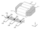
図2は、昇圧リアクトルと負荷に供給される電流用の各電流センサ素子との間の位置関係例を示す斜視図である。インバータ回路20から負荷2への電流供給は、バスバ23a〜23cを介して行われる。各電流センサ素子22a〜22cは、図2に示すように、バスバ23a〜23cに隣接して設置される。
FIG. 2 is a perspective view showing an example of a positional relationship between the boost reactor and each current sensor element for supplying a current to a load. The current supply from the inverter circuit 20 to the load 2 is performed via the bus bars 23a to 23c. Each of the
各電流センサ素子22a〜22cは、上記のように、磁束に応じた信号を出力する素子である。各バスバ23a〜23cに流れる電流を高精度に検出するためには、バスバ23a〜23cがそれぞれ発生させる磁束のみを各電流センサ素子22a〜22cに検出させるようにする必要がある。しかし、電力変換装置100には、対象とする磁束以外の磁束を発生させる外乱磁場が存在する。電力変換装置100において、昇圧リアクトル12は、最も強い外乱磁場を発生させる磁性部品である。このことから、図2では、昇圧リアクトル12と各電流センサ素子22a〜22cの位置関係例を示している。
Each of the
本実施の形態1では、図2に示すように、各電流センサ素子22a〜22cを挟み込むように、2つの磁気シールド板24a、24bを対向配置している。これら磁気シールド板24a、24bは、磁束の遮蔽のために、高比透磁率の磁性材料を用いて作製した部材である。その磁性材料としては、比透磁率が3000以上のものが好ましい。この条件を満たす磁性材料としては、パーマロイ、純鉄、Fe−6.5Si、Fe−3.5Si、Fe基アモルファス、ナノ結晶Fe基、軟磁性材料、珪素鋼板等を挙げることができる。
In the first embodiment, as shown in FIG. 2, two
以降、説明上、便宜的に、特定する必要のない磁気シールド板には「24」を符号として付すこととする。同様に、特定する必要のない1つ以上の電流センサ素子には「22」を符号として付すこととし、特定する必要のない1つ以上のバスバには「23」を符号として付すこととする。 Hereinafter, for the sake of convenience in description, a magnetic shield plate that does not need to be specified is denoted by “24”. Similarly, one or more current sensor elements that do not need to be specified are denoted by reference numeral “22”, and one or more bus bars that do not need to be specified are denoted by reference numeral “23”.
図3は、昇圧リアクトルと負荷に供給される電流用の各電流センサ素子との間の位置関係例を示す平面図であり、図4は、昇圧リアクトルと負荷に供給される電流用の各電流センサ素子との間の位置関係例を示す側面図である。 FIG. 3 is a plan view showing an example of a positional relationship between the boost reactor and each current sensor element for a current supplied to the load. FIG. 4 is a plan view showing each current sensor element for the current supplied to the load and the boost reactor. It is a side view which shows the example of a positional relationship with a sensor element.
図3に示す平面図は、図2中、Z軸上、正側からの視点、つまりZ軸上、値の大きい側から値の小さい側を向いた視点での図であり、図4に示す側面図は、図2中、X軸方向上、負側からの視点の図である。ここで、図3、及び図4を参照し、磁気シールド板24について具体的に説明する。この図3及び図4では、説明上、便宜的に、磁気シールド板24は1つのみ示している。
The plan view shown in FIG. 3 is a view from the viewpoint from the positive side on the Z axis in FIG. 2, that is, from the viewpoint on the Z axis from the side with the larger value to the side with the smaller value. The side view is a view from the negative side in the X-axis direction in FIG. Here, the
図3において、矢印A1は、各バスバ23a〜23cに流れる電流の向きを示している。このことから、バスバ23a〜23cに流れる電流にも「A1」を符号として付すこととする。F1は、昇圧リアクトル12が発生する磁束のなかで、電流センサ素子22に向かう磁束を表している。矢印F2は、図4にも示すように、電流A1がバスバ23aを流れることによって発生する磁束を表している。図3では、XY平面上で磁束の向きを矢印により示している。この磁束F2は、電流センサ素子22aが最も高感度に磁束を検出する感磁方向と略一致する。磁束F2の向きは、他のバスバ23b、23cでも基本的に同じであり、感磁方向は全ての電流センサ素子22a〜22cで基本的に同じである。
In FIG. 3, an arrow A1 indicates a direction of a current flowing through each of the bus bars 23a to 23c. For this reason, "A1" is also given as a code to the current flowing through the bus bars 23a to 23c. F1 represents a magnetic flux directed toward the
図3及び図4に示すように、磁気シールド板24は、昇圧リアクトル12と電流センサ素子22とを結ぶ直線上に配置されている。より具体的には、磁気シールド板24は、電流センサ素子22a〜22cの配列方向に沿って、3本のバスバ23a〜23cを横切るようにして、昇圧リアクトル12と電流センサ素子22との間に配置されている。磁気シールド板24は、昇圧リアクトル12が発生する磁束F1のなかで、電流センサ素子22が検出可能な方向範囲内からその電流センサ素子22に到達する磁束F1を遮蔽可能な形状となっている。そのため、磁気シールド板24は、昇圧リアクトル12が発生した磁束F1が電流センサ素子22に検出されることを回避させるか、或いは検出される磁束を大きく抑制させる働きをする。
As shown in FIGS. 3 and 4, the
電流センサ素子22と直線を結ぶ昇圧リアクトル12上の位置としては、例えば昇圧リアクトル12で磁束を発生させる部分のXZ平面上の中心が考えられる。複数の電流センサ素子22に対し、同じ1つの磁気シールド板24を用いるのであれば、複数の電流センサ素子22の中心に位置する電流センサ素子22、或いは複数の電流センサ素子22が並ぶ方向上の中心となる位置が考えられる。昇圧リアクトル12、電流センサ素子22共に、直線を結ぶ位置は適宜、定めても良いものであり、その位置は仮想的な位置であっても良い。
The position on the step-up
磁気シールド板24は、図3及び図4に示すように、板状の部材である。その磁気シールド板24は、各バスバ23a〜23cに電流A1が流れることによって発生する磁束F2が電流センサ素子22に到達するのを遮蔽しないように配置されている。これらの結果、電流センサ素子22には、バスバ23が発生する磁束F2のみが通るか、通る磁束の大部分はバスバ23が発生させたものとなる。従って、磁気シールド板24を配置することにより、電流センサ素子22を用いた電流A1の測定を高精度に行うことができる。
The
磁気シールド板24の配置、及び形状の決定は、特許文献1に記載の従来技術とは異なり、各バスバ23、各電流センサ素子22a〜22c、及び昇圧リアクトルの配置の決定とは別に独立して行うことができる。そのため、磁気シールド板24の配置に伴い、電力変換装置100の設計上の自由度を抑制するようなことは回避されるか、或いはその抑制の程度は非常に低いレベルとなる。
The arrangement and the shape of the
本実施の形態1では、図3及び図4に示すように、昇圧リアクトル12からの磁束F1を含む平面上に各電流センサ素子22a〜22cを配置している。このように各電流センサ素子22a〜22c、各バスバ23a〜23cを配置した場合、各電流センサ素子22a〜22cに共通の磁気シールド板24を用いることができる。この磁気シールド板24のZ軸方向上の必要な長さ、つまり高さも抑えられる。これらのことから、部品点数の抑制、磁気シールド板24の取付性等の面での利点が得られる。
In the first embodiment, as shown in FIGS. 3 and 4, each of
図5は、磁界シミュレーションのための昇圧リアクトル、電流センサ素子、及び2つの磁気シールド板の間の位置関係を示す斜視図であり、図6は、磁界シミュレーションの結果を示す図である。次に、図5及び図6を参照し、磁気シールド板24による遮蔽効果について具体的に説明する。
FIG. 5 is a perspective view illustrating a positional relationship between a boost reactor, a current sensor element, and two magnetic shield plates for a magnetic field simulation, and FIG. 6 is a diagram illustrating a result of the magnetic field simulation. Next, the shielding effect of the
図5及び図6において、同じ構成要素、或いは相当する構成要素には対応する符号を付している。電流センサ素子22は、図3に示す電流センサ素子22bに相当する。図6に示す磁界シミュレーション結果は、電流センサ素子22を含むXY平面に、電流センサ素子22の感磁方向であるX軸方向での磁束の大きさを濃淡により表している。濃くなるほど、磁束が大きいことを表している。磁界シミュレーションでは、磁気シールド板24による遮蔽効果の確認を容易とするために、バスバ23は模擬しないこととしている。
5 and 6, the same components or corresponding components are denoted by corresponding reference numerals. The
図6に示すように、磁気シールド板24aは、昇圧リアクトル12からの磁束F1を遮蔽することから、その磁気シールド板24aからY軸上、負方向側の磁束は非常に小さくなっている。2つの磁気シールド板24a、24b間において、磁束が非常に小さくなっているX軸上の範囲は、Y軸上、負方向側に向けて、徐々に狭くなった後、徐々に広くなる。
As shown in FIG. 6, since the
磁束が非常に小さくなるX軸上の範囲がY軸上、負方向側に向けて徐々に広くなるのは、磁気シールド板24b内に磁束F1が迂回されるからである。その迂回により、Y軸上、磁気シールド板24に近づくほど、磁束が非常に小さくなっているX軸上の範囲は広くなる。
The reason why the range on the X-axis where the magnetic flux becomes extremely small gradually increases toward the negative direction side on the Y-axis is because the magnetic flux F1 is bypassed in the
このことから、磁束が非常に小さくなるX軸上の範囲のY軸上の位置による図6に示すような変化は、磁気シールド板24aはもとより、磁気シールド板24bも有効であることを示している。つまり磁気シールド板24a及び磁気シールド板24bは共に、電流センサ素子22が磁束を検出可能な感度領域内の不要な磁束を抑制する。この事実から、電流A1をより高精度に測定するうえで、電流センサ素子22を挟むように2つの磁気シールド板24を配置することは非常に有効である。
From this, the change as shown in FIG. 6 depending on the position on the Y-axis in the range on the X-axis where the magnetic flux becomes very small indicates that not only the
図5に示すようなモデルの磁界シミュレーションにより、電流センサ素子22の感磁方向上の磁気シールド板24の長さは、その感磁方向上の電流センサ素子22の長さの2倍よりも長くするのが好ましいことが確認された。感磁方向は、好ましくは、最も高感度に磁束を検出する感磁方向である。磁気シールド板24の好ましい長さは、電流センサ素子22との距離が長くなるほど、長くなる。以降、感磁方向上の電流センサ素子の長さを「素子長」と表記する。
According to the magnetic field simulation of the model as shown in FIG. 5, the length of the
磁気シールド板24は、図2及び図3に示すように、3つの電流センサ素子22a〜22cに対して1つ設けることもできる。その場合、磁気シールド板24の好ましい長さは、3つの電流センサ素子22a〜22cの配列方向上の端から端までの長さに、素子長よりも大きい長さを加えた長さとなる。つまり、磁気シールド板24の好ましい長さは、対象とする電流センサ素子22の数に係わらず、対象とする電流センサ素子22が存在する範囲の長さに、素子長よりも大きい長さを加えた長さとなる。
As shown in FIGS. 2 and 3, one
なお、本実施の形態1では、磁気シールド板24を2つ配置しているが、磁気シールド板24は1つとしても良い。この場合、磁気シールド板24は、より大きくするのが好ましい。位置は、昇圧リアクトル12からの視点において、電流センサ素子22の手前側であっても良いが、電流センサ素子22の奥側であっても良い。
In the first embodiment, two
また、1つ以上の磁気シールド板24を、電流センサ素子22毎に設けても良い。磁気シールド板24の形状は、平面状ではなく、曲面状であっても良い。複数の平面を組み合わせたような形状であっても良い。これらのこともあり、磁気シールド板24の配置の仕方、その形状等は、様々な変形が可能である。
One or more
また、電力変換装置100は、DCDC昇圧コンバータ回路10、インバータ回路20を有したものであるが、本実施の形態1を適用可能な電力変換装置100は、そのような装置に限定されない。例えば電力変換装置100は、AC/DCコンバータ回路を有するもの、絶縁型DCDCコンバータ回路を有するもの、等であっても良く、3つ以上の回路を有するものであっても良い。つまり、電力変換装置100は、非接触で電流A1の検出に用いる電流センサ素子、及びその電流センサ素子の検出結果に影響を及ぼす磁性部品を有するものであれば良い。
Further, the
実施の形態2.
DCDC昇圧コンバータ回路10の半導体スイッチング素子13a〜13dをスイッチング動作させた場合、昇圧リアクトル12が有する2つの巻線122にはリプル成分を持った電流が流れる。そのため、昇圧リアクトル12が発生させる磁束F1は、このリプル成分に応じて変化する。昇圧リアクトル12が発生する磁束F1を完全に遮蔽できない場合、その磁束F1の変化は、電流値の検出結果に含まれる誤差の大きさを変動させ、磁気シールド板24を発熱させる。このことから、本実施の形態2は、電流値の検出結果に含まれる誤差の大きさの変動を抑制して、精度をより向上させると共に、磁気シールド板24の発熱をより抑えるようにしたものである。ここでは、上記実施の形態1と同じ、或いは相当する構成要素には同じ符号を付し、異なる部分について詳細に説明する。これは、後述する他の実施の形態でも同様とする。
Embodiment 2 FIG.
When the
図7は、本発明の実施の形態2に係る電力変換装置が収められた筐体内での昇圧リアクトル、バスバ、電流センサ素子、及び磁気シールド板の配置例を示す断面図である。この断面図は、X軸方向上、負側からの視点のものである。 FIG. 7 is a cross-sectional view illustrating an example of the arrangement of a boost reactor, a bus bar, a current sensor element, and a magnetic shield plate in a housing accommodating the power converter according to Embodiment 2 of the present invention. This cross-sectional view is taken from the negative side in the X-axis direction.
電力変換装置100は、筐体5内に設けられる。本実施の形態2では、図7に示すように、磁気シールド板24に加え、金属シールド板5aが昇圧リアクトル12と電流センサ素子22とを結ぶ直線上に配置されている。すなわち、金属シールド板5aは、電流センサ素子22a〜22cの配列方向に沿って、磁気シールド板24と平行か、或いは略並行に、昇圧リアクトル12と電流センサ素子22との間に配置されている。そして、金属シールド板5aは、昇圧リアクトル12と磁気シールド板24との間に配置されている。
The
金属シールド板5aは、アルミニウム、銅、ステンレス等の非磁性体であり、かつ電気伝導率の高い材料で作製された板状部材であり、昇圧リアクトル12から電流センサ素子22に向かう磁束F1が通る範囲をカバーする大きさである。そのため、金属シールド板5aは、渦電流による磁気遮蔽効果によって、昇圧リアクトル12から電流センサ素子22に向かう磁束F1を遮断するようになっている。したがって、昇圧リアクトル12が発生させる時間変化を伴う磁束F1は、金属シールド板5aによって遮断され、電流センサ素子22および磁気シールド板24に影響を与えないか、或いはその影響を大幅に抑制される。この結果、上記実施の形態1と比較し、本実施の形態2では、電流値の測定を、より高精度に行うことができる。
The
なお、金属シールド板5aは、筐体5の一部として実現させているが、個別の部品として作製しても良い。筐体5の一部として金属シールド板5aを実現させた場合、部品点数の低減、組立コストの抑制等の面で利点がある。
Although the
実施の形態3.
図8は、本発明の実施の形態3に係る電力変換装置におけるバスバを含む周辺の構成例と昇圧リアクトルとの間の位置関係例を示す斜視図である。
Embodiment 3 FIG.
FIG. 8 is a perspective view showing an example of a positional relationship between a configuration example around a bus bar and a boost reactor in a power converter according to Embodiment 3 of the present invention.
本実施の形態3では、図8に示すように、各電流センサ素子22を挟む位置に2つの磁気シールド板24a、24bが配置され、各電流センサ素子22には、それぞれ集磁コア25a〜25cが更に配置されている。
In the third embodiment, as shown in FIG. 8, two
各集磁コア25a〜25cは、対応するバスバ23が発生させた磁束数を増幅し、対応する電流センサ素子22に供給する部品である。そのために、各集磁コア25a〜25cは、バスバ23が発生する磁束F2のなかで電流センサ素子22に供給される磁束F2の磁路上に設置される。
Each of the magnetic
このような集磁コア25a〜25cを用いることにより、電流センサ素子22のS/N比(Signal-to-Noise ratio)をより向上させることができる。従って、バスバ23の電流値もより高精度に検出することができる。また、集磁コア25a〜25cは、自身が磁気シールドとしての効果を有する。これは、集磁コア25a〜25cを用いることにより、外乱磁界への耐性がより高くなることを意味する。このことも、バスバ23の電流値をより高精度に検出できるように機能する。
By using such magnetic
各磁気シールド板24は、図8に示すように、集磁コア25a〜25cが集磁する磁束F2の磁路上を避けて配置されている。そのため、磁気シールド板24によって電流センサ素子22のS/N比を低下させるようなことは回避される。
As shown in FIG. 8, each
実施の形態4.
図9は、本発明の実施の形態4に係る電力変換装置におけるバスバを含む周辺の構成例と昇圧リアクトルとの間の位置関係例を示す斜視図である。
Embodiment 4 FIG.
FIG. 9 is a perspective view showing an example of a positional relationship between a configuration example around a bus bar and a boost reactor in a power conversion device according to Embodiment 4 of the present invention.
本実施の形態4では、図9に示すように、上記実施の形態3から、各集磁コア25a〜25cを含む範囲をカバーする磁気シールド板26が追加されている。この磁気シールド板26は、各集磁コア25a〜25cのZ軸上、負側に配置されている。
In the fourth embodiment, as shown in FIG. 9, a
集磁コア25a〜25cは、例えば複種類の磁性部材を積層して作製された部品である。この磁性部材に磁束が供給されることにより、電流センサ素子22に供給される磁束が変化する。磁気シールド板26を配置することにより、外乱磁場による磁束が集磁コア25a〜25cに到達するのを抑制することができる。そのため、上記実施の形態3と比較し、バスバ23の電流値をより高精度に測定することができる。
The magnetic
集磁コア25a〜25cの電流センサ素子22の感度方向上の長さを「コア長」と表記する。その感度方向上の磁気シールド板26の好ましい長さは、対象が集磁コア25a〜25cのうちの1つであった場合、コア長の2倍よりも大きい長さである。図9に示すように、集磁コア25a〜25cに対して1つの磁気シールド板26を設ける場合、磁気シールド板26の好ましい長さは、対象とする集磁コア25a〜25cが存在する範囲の長さに、コア長よりも大きい長さを加えた長さとなる。
The length of the magnetic
なお、上記実施の形態1〜4では、電流センサ素子22に影響を及ぼす外乱磁場を発生させる磁性部品として昇圧リアクトルを想定しているが、想定する磁性部品は、昇圧リアクトルに限定されない。想定する磁性部品は、電力変換装置100に用いられる磁性部品、その位置関係等により、決定すれば良いものである。つまり磁性部品は、例えば比較的に透磁率の低いダストコアを用いたリアクトル、トランス等であっても良い。想定する磁性部品は複数であっても良い。例えば磁気シールド板26は、別の磁性部品が発生する磁束の遮蔽用に配置しても良い。
In the first to fourth embodiments, the boosting reactor is assumed as the magnetic component that generates a disturbance magnetic field that affects the
また、上記実施の形態1〜4は、組み合わせが可能である。例えば金属シールド板5aは、上記実施の形態3及び4で用いても良い。その場合、磁気シールド板24は一つのみ配置するようにしても良い。
Further, the first to fourth embodiments can be combined. For example, the
1 電源、2 負荷、5 筐体、5a 金属シールド板、10 DCDC昇圧コンバータ回路、12 昇圧リアクトル(磁性部品)、20 インバータ回路、22、22a〜22c 電流センサ素子、23、23a〜23c バスバ、24、24a、24b、26 磁気シールド板、25a〜25c 集磁コア、100 電力変換装置、121 磁心、122 巻線。
REFERENCE SIGNS
Claims (15)
負荷に電力を供給するための複数のバスバと、
バスバ毎に設けられ、前記バスバに電流が流れることにより発生する磁束を検出する電流センサ素子と、
前記磁性部品と前記電流センサ素子とを結ぶ直線上に配置され、前記磁性部品から前記電流センサ素子に向かう磁束を遮蔽する板状の磁気シールド板と、
を備える電力変換装置。 A power converter that converts the power supplied from the power supply using a magnetic component,
A plurality of bus bars for supplying power to the load;
A current sensor element that is provided for each bus bar and detects a magnetic flux generated when a current flows through the bus bar;
A plate-shaped magnetic shield plate that is arranged on a straight line connecting the magnetic component and the current sensor element and shields magnetic flux from the magnetic component toward the current sensor element;
A power conversion device comprising:
請求項1に記載の電力変換装置。 The magnetic shield plate has a shape determined based on a magnetic sensing direction in which the magnetic flux of the current sensor element can be detected, and a magnetic flux directed from the magnetic component toward the current sensor element.
The power converter according to claim 1.
請求項1または2に記載の電力変換装置。 The magnetic shield plate is disposed avoiding a magnetic sensing direction in which the magnetic flux of the current sensor element can be detected,
The power converter according to claim 1.
請求項1〜3の何れか1項に記載の電力変換装置。 A plurality of the magnetic shield plates are arranged;
The power converter according to claim 1.
請求項4記載の電力変換装置。 The two or more magnetic shield plates are opposed to each other at a position sandwiching the current sensor element.
The power converter according to claim 4.
請求項2〜5の何れか1項に記載の電力変換装置。 The length of the magnetic shield plate in the magnetic sensing direction is greater than the length of the current sensor element in the magnetic sensing direction in a range in the magnetic sensing direction in which the target current sensor element exists. It is the length plus the length,
The power converter according to any one of claims 2 to 5.
前記磁気シールド板は、前記バスバ毎に設けられる各電流センサ素子を対象に、前記複数のバスバを横切るように配置されている、
請求項1〜6の何れか1項に記載の電力変換装置。 The plurality of bus bars are installed adjacent to each other,
The magnetic shield plate, for each current sensor element provided for each bus bar, is disposed to cross the plurality of bus bars,
The power converter according to any one of claims 1 to 6.
を更に備える請求項1〜7の何れか1項に記載の電力変換装置。 A metal plate disposed between the magnetic component and the magnetic shield plate,
The power converter according to any one of claims 1 to 7, further comprising:
請求項8に記載の電力変換装置。 The metal plate is a part of a housing,
A power converter according to claim 8.
を更に備える請求項1〜9の何れか1項に記載の電力変換装置。 A magnetic flux collecting core that is provided for each of the current sensor elements and collects a magnetic flux generated when a current flows through the bus bar;
The power converter according to any one of claims 1 to 9, further comprising:
を更に備える請求項10記載の電力変換装置。 Another magnetic shield plate arranged for the magnetic flux collecting core,
The power conversion device according to claim 10, further comprising:
請求項11に記載の電力変換装置。 The length of the other magnetic shield plate in the magnetic sensing direction is a length in the magnetic sensing direction in which the target magnetic collecting core is present, and a length of the magnetic collecting core in the magnetic sensing direction. It is the length which added the length larger than
The power converter according to claim 11.
請求項11または12に記載の電力変換装置。 The other magnetic shield plate is manufactured using a magnetic material,
The power converter according to claim 11.
請求項1〜13の何れか1項に記載の電力変換装置。 The magnetic shield plate is manufactured using a magnetic material,
The power converter according to any one of claims 1 to 13.
請求項1〜14の何れか1項に記載の電力変換装置。 The magnetic component is a reactor that has a plurality of windings having a turn ratio of 1 to 1 on a common magnetic core, and the plurality of windings generates magnetic flux in a direction to cancel each other in the magnetic core.
The power converter according to any one of claims 1 to 14.
Priority Applications (5)
| Application Number | Priority Date | Filing Date | Title |
|---|---|---|---|
| JP2018120984A JP6472561B1 (en) | 2018-06-26 | 2018-06-26 | Power converter |
| EP19824600.1A EP3817214B1 (en) | 2018-06-26 | 2019-04-01 | Power conversion device |
| PCT/JP2019/014504 WO2020003674A1 (en) | 2018-06-26 | 2019-04-01 | Power conversion device |
| CN201980041650.1A CN112313865A (en) | 2018-06-26 | 2019-04-01 | Power conversion device |
| US17/051,021 US11515801B2 (en) | 2018-06-26 | 2019-04-01 | Shield in a power conversion device |
Applications Claiming Priority (1)
| Application Number | Priority Date | Filing Date | Title |
|---|---|---|---|
| JP2018120984A JP6472561B1 (en) | 2018-06-26 | 2018-06-26 | Power converter |
Publications (2)
| Publication Number | Publication Date |
|---|---|
| JP6472561B1 JP6472561B1 (en) | 2019-02-20 |
| JP2020005367A true JP2020005367A (en) | 2020-01-09 |
Family
ID=65443088
Family Applications (1)
| Application Number | Title | Priority Date | Filing Date |
|---|---|---|---|
| JP2018120984A Active JP6472561B1 (en) | 2018-06-26 | 2018-06-26 | Power converter |
Country Status (5)
| Country | Link |
|---|---|
| US (1) | US11515801B2 (en) |
| EP (1) | EP3817214B1 (en) |
| JP (1) | JP6472561B1 (en) |
| CN (1) | CN112313865A (en) |
| WO (1) | WO2020003674A1 (en) |
Families Citing this family (2)
| Publication number | Priority date | Publication date | Assignee | Title |
|---|---|---|---|---|
| JP6825023B2 (en) * | 2019-02-27 | 2021-02-03 | 三菱電機株式会社 | Power converter |
| JP6818844B1 (en) * | 2019-10-28 | 2021-01-20 | 三菱電機株式会社 | Power converter |
Citations (4)
| Publication number | Priority date | Publication date | Assignee | Title |
|---|---|---|---|---|
| JP2005321206A (en) * | 2004-05-06 | 2005-11-17 | Mitsubishi Electric Corp | Current detection device |
| JP2012065431A (en) * | 2010-09-15 | 2012-03-29 | Aisin Aw Co Ltd | Inverter device |
| JP2013013169A (en) * | 2011-06-28 | 2013-01-17 | Toyota Motor Corp | Power conversion apparatus and electric vehicle including the same |
| JP2018033266A (en) * | 2016-08-25 | 2018-03-01 | 株式会社デンソー | Current sensor device |
Family Cites Families (34)
| Publication number | Priority date | Publication date | Assignee | Title |
|---|---|---|---|---|
| DE59712967D1 (en) * | 1997-05-21 | 2008-10-30 | Landis & Gyr Ag | Arrangement for obtaining a proportional to an electric current magnetic induction at the location of a magnetic field sensor |
| US6570141B2 (en) * | 2001-03-26 | 2003-05-27 | Nicholas V. Ross | Transverse flux induction heating of conductive strip |
| JP4551166B2 (en) * | 2004-09-13 | 2010-09-22 | 矢崎総業株式会社 | Device direct connector |
| JP2006112968A (en) * | 2004-10-15 | 2006-04-27 | Toyota Motor Corp | Current detecting device |
| JP5207085B2 (en) * | 2010-03-09 | 2013-06-12 | アイシン・エィ・ダブリュ株式会社 | Current detector |
| JP5714528B2 (en) * | 2012-03-19 | 2015-05-07 | 株式会社豊田中央研究所 | Power converter and power system |
| JP6372969B2 (en) * | 2012-12-03 | 2018-08-15 | 矢崎総業株式会社 | Current sensor |
| JP6477089B2 (en) * | 2014-05-23 | 2019-03-06 | 株式会社デンソー | Bus bar module with current sensor |
| DE102014119276A1 (en) * | 2014-12-19 | 2016-06-23 | Micronas Gmbh | current sensor |
| JP6149885B2 (en) * | 2015-03-18 | 2017-06-21 | トヨタ自動車株式会社 | Current sensor |
| JP2016200549A (en) * | 2015-04-14 | 2016-12-01 | トヨタ自動車株式会社 | Current-voltage sensor |
| WO2017149776A1 (en) * | 2016-03-04 | 2017-09-08 | 三菱電機株式会社 | Power conversion device |
| JP6711086B2 (en) * | 2016-04-01 | 2020-06-17 | 日立金属株式会社 | Current sensor |
| JP6651956B2 (en) * | 2016-04-01 | 2020-02-19 | 日立金属株式会社 | Current sensor |
| JP2017204981A (en) | 2016-05-13 | 2017-11-16 | 株式会社Soken | Power converter |
| JP6690433B2 (en) * | 2016-06-28 | 2020-04-28 | 日立金属株式会社 | Current sensor |
| JP2018080944A (en) * | 2016-11-14 | 2018-05-24 | 株式会社Soken | Current sensor |
| JP2018169305A (en) * | 2017-03-30 | 2018-11-01 | 日立金属株式会社 | Current sensor |
| JP2018185230A (en) * | 2017-04-26 | 2018-11-22 | 株式会社デンソー | Current sensor |
| JP6503413B2 (en) * | 2017-05-31 | 2019-04-17 | 本田技研工業株式会社 | DC / DC converter and electrical equipment |
| JP6375020B2 (en) | 2017-06-13 | 2018-08-15 | 株式会社タムラ製作所 | Current sensor device |
| JP6395166B1 (en) * | 2017-07-10 | 2018-09-26 | 三菱電機株式会社 | Power converter |
| JP7003608B2 (en) * | 2017-12-05 | 2022-01-20 | 日立金属株式会社 | Current sensor |
| WO2019117169A1 (en) * | 2017-12-13 | 2019-06-20 | アルプスアルパイン株式会社 | Current sensor |
| JP7003620B2 (en) * | 2017-12-14 | 2022-01-20 | 日立金属株式会社 | Current sensor |
| JP6973021B2 (en) * | 2017-12-18 | 2021-11-24 | 日立金属株式会社 | Current sensor |
| JP7047435B2 (en) * | 2018-02-13 | 2022-04-05 | 日立金属株式会社 | How to design a current sensor |
| JP7172079B2 (en) * | 2018-03-20 | 2022-11-16 | 株式会社デンソー | current sensor |
| JP2020012671A (en) * | 2018-07-13 | 2020-01-23 | 日立金属株式会社 | Current sensor |
| KR102258813B1 (en) * | 2018-11-20 | 2021-05-31 | 주식회사 엘지에너지솔루션 | Hybrid type current measuring device |
| JP6825023B2 (en) * | 2019-02-27 | 2021-02-03 | 三菱電機株式会社 | Power converter |
| JP7093747B2 (en) * | 2019-06-07 | 2022-06-30 | 本田技研工業株式会社 | Power control unit and drive unit |
| JP7295262B2 (en) * | 2019-10-08 | 2023-06-20 | アルプスアルパイン株式会社 | current detector |
| JP7242887B2 (en) * | 2019-10-08 | 2023-03-20 | アルプスアルパイン株式会社 | current detector |
-
2018
- 2018-06-26 JP JP2018120984A patent/JP6472561B1/en active Active
-
2019
- 2019-04-01 CN CN201980041650.1A patent/CN112313865A/en active Pending
- 2019-04-01 WO PCT/JP2019/014504 patent/WO2020003674A1/en unknown
- 2019-04-01 US US17/051,021 patent/US11515801B2/en active Active
- 2019-04-01 EP EP19824600.1A patent/EP3817214B1/en active Active
Patent Citations (4)
| Publication number | Priority date | Publication date | Assignee | Title |
|---|---|---|---|---|
| JP2005321206A (en) * | 2004-05-06 | 2005-11-17 | Mitsubishi Electric Corp | Current detection device |
| JP2012065431A (en) * | 2010-09-15 | 2012-03-29 | Aisin Aw Co Ltd | Inverter device |
| JP2013013169A (en) * | 2011-06-28 | 2013-01-17 | Toyota Motor Corp | Power conversion apparatus and electric vehicle including the same |
| JP2018033266A (en) * | 2016-08-25 | 2018-03-01 | 株式会社デンソー | Current sensor device |
Also Published As
| Publication number | Publication date |
|---|---|
| WO2020003674A1 (en) | 2020-01-02 |
| EP3817214A1 (en) | 2021-05-05 |
| US11515801B2 (en) | 2022-11-29 |
| JP6472561B1 (en) | 2019-02-20 |
| EP3817214B1 (en) | 2022-06-22 |
| US20210143745A1 (en) | 2021-05-13 |
| EP3817214A4 (en) | 2021-08-25 |
| CN112313865A (en) | 2021-02-02 |
Similar Documents
| Publication | Publication Date | Title |
|---|---|---|
| JP6350785B2 (en) | Inverter device | |
| US20130169267A1 (en) | Current sensor | |
| JPH10307156A (en) | Method and device for measuring current in n conductors | |
| US20110221430A1 (en) | Current detection device | |
| JP5699993B2 (en) | Inverter | |
| JP2010008050A (en) | Current sensor | |
| JP5234459B2 (en) | Current sensor | |
| JP2020537141A (en) | Current sensor assembly | |
| US11796571B2 (en) | Busbar and power module with busbar | |
| JP5456171B2 (en) | Multiphase DC voltage converter and control method of multiphase DC voltage converter | |
| WO2020003674A1 (en) | Power conversion device | |
| JP2005321206A (en) | Current detection device | |
| US11688548B2 (en) | Power conversion device | |
| JP5859273B2 (en) | Distribution board | |
| KR20100029390A (en) | Current detecting device of inverter for hev | |
| US11493537B2 (en) | Magnetic field-based current sensor for frequency-compensated measurement of alternating currents | |
| JP5945975B2 (en) | Bus bar module | |
| Dianov | Recommendations and typical errors in design of power converter PCBs with shunt sensors | |
| Kim et al. | Coreless hall current sensor for automotive inverters decoupling cross-coupled field | |
| JP2012063285A (en) | Current sensor | |
| Sirat | Ultra-Wideband Contactless Current Sensors for Power Electronics Applications | |
| JP2016200549A (en) | Current-voltage sensor | |
| JP5560232B2 (en) | Current detector | |
| JP2014055839A (en) | Current detector | |
| JP2020012671A (en) | Current sensor |
Legal Events
| Date | Code | Title | Description |
|---|---|---|---|
| A621 | Written request for application examination |
Free format text: JAPANESE INTERMEDIATE CODE: A621 Effective date: 20180626 |
|
| TRDD | Decision of grant or rejection written | ||
| A01 | Written decision to grant a patent or to grant a registration (utility model) |
Free format text: JAPANESE INTERMEDIATE CODE: A01 Effective date: 20181225 |
|
| A61 | First payment of annual fees (during grant procedure) |
Free format text: JAPANESE INTERMEDIATE CODE: A61 Effective date: 20190122 |
|
| R150 | Certificate of patent or registration of utility model |
Ref document number: 6472561 Country of ref document: JP Free format text: JAPANESE INTERMEDIATE CODE: R150 |
|
| R250 | Receipt of annual fees |
Free format text: JAPANESE INTERMEDIATE CODE: R250 |
|
| R250 | Receipt of annual fees |
Free format text: JAPANESE INTERMEDIATE CODE: R250 |
|
| R250 | Receipt of annual fees |
Free format text: JAPANESE INTERMEDIATE CODE: R250 |