JP2020005259A - Semiconductor device - Google Patents
Semiconductor device Download PDFInfo
- Publication number
- JP2020005259A JP2020005259A JP2019133009A JP2019133009A JP2020005259A JP 2020005259 A JP2020005259 A JP 2020005259A JP 2019133009 A JP2019133009 A JP 2019133009A JP 2019133009 A JP2019133009 A JP 2019133009A JP 2020005259 A JP2020005259 A JP 2020005259A
- Authority
- JP
- Japan
- Prior art keywords
- oscillation signal
- circuit
- buffer
- supplied
- power supply
- Prior art date
- Legal status (The legal status is an assumption and is not a legal conclusion. Google has not performed a legal analysis and makes no representation as to the accuracy of the status listed.)
- Granted
Links
Images


Landscapes
- Logic Circuits (AREA)
- Inductance-Capacitance Distribution Constants And Capacitance-Resistance Oscillators (AREA)
Abstract
【課題】周波数の異なる発振信号間におけるクロストークの影響を抑制する。【解決手段】半導体装置1は、少なくとも第1の電源系統から電力が供給される第1の回路部と、第1の電源系統とは異なる第2の電源系統から電力が供給される第2の回路部とを備える。第1の回路部は、第1の電源系統から電力が供給され、且つ、第1の発振信号生成回路により生成された第1の発振信号が入力される第1のバッファを備える。第1のバッファは、第1の制御信号に基づいて、第2の回路部に1の発振信号を出力するか否かを制御する。第2のバッファは、第2の電源系統から電力が供給され、第2の発振信号生成回路により生成された第2の発振信号が2の回路部から入力される。第2のバッファは、第2の制御信号に基づいて、入力された第2の発振信号を、第1の電源系統から電力が供給される第1の処理部に出力するか否かを制御する。【選択図】図1An object of the present invention is to suppress the influence of crosstalk between oscillation signals having different frequencies. A semiconductor device (1) includes a first circuit section to which power is supplied from at least a first power supply system, and a second circuit section to which power is supplied from a second power supply system different from the first power supply system. and a circuit unit. The first circuit section includes a first buffer to which power is supplied from the first power supply system and to which the first oscillation signal generated by the first oscillation signal generation circuit is input. The first buffer controls whether to output one oscillation signal to the second circuit unit based on the first control signal. The second buffer is supplied with power from the second power supply system and receives the second oscillation signal generated by the second oscillation signal generating circuit from the second circuit section. The second buffer controls whether or not to output the input second oscillation signal to the first processing unit to which power is supplied from the first power supply system, based on the second control signal. . [Selection drawing] Fig. 1
Description
本発明の実施形態は、半導体装置に関する。 Embodiments of the present invention relate to a semiconductor device.
無線通信において、送信側と受信側の双方で複数のチャネルを用いて通信を行うための規格としてMIMO(Multiple Input and Multiple Output)が提唱されている。さらに、MIMOを部分的にマルチユーザ化したマルチユーザMIMOの実用化に向けた研究開発も盛んに行われている。 In wireless communication, MIMO (Multiple Input and Multiple Output) has been proposed as a standard for performing communication using a plurality of channels on both a transmitting side and a receiving side. Further, research and development for the practical use of multi-user MIMO in which MIMO is partially made multi-user has been actively performed.
このような通信環境を実現するためには、1つの半導体装置内において、送信器や受信器で必要となるIQ変調信号を発生するIQ信号発生器に、周波数が近接している2つの発振信号を供給する必要がある。しかし、周波数の近接している2つの発振信号の伝送路を並走させると、伝送路間におけるクロストークの問題が生じる。 In order to realize such a communication environment, two oscillation signals having frequencies close to an IQ signal generator for generating an IQ modulation signal required for a transmitter or a receiver in one semiconductor device. Need to be supplied. However, if two transmission lines of oscillation signals having frequencies close to each other are run in parallel, a problem of crosstalk between the transmission lines occurs.
また、複数設けられたIQ信号発生器に、2つの発振信号を切り替えて供給すために切替スイッチを設ける必要があるが、この切替スイッチにおいても、近接する切替スイッチの間でクロストークの問題が生じる。 Further, it is necessary to provide a changeover switch for switching and supplying two oscillation signals to a plurality of IQ signal generators. Even in this changeover switch, a problem of crosstalk between adjacent changeover switches is required. Occurs.
本実施形態の目的は、周波数の異なる発振信号間におけるクロストークの影響を抑制した半導体装置を提供することにある。 An object of the present embodiment is to provide a semiconductor device in which the influence of crosstalk between oscillation signals having different frequencies is suppressed.
本実施形態に係る半導体装置は、第1の電源系統から電力が供給される第1の回路部と、第1の電源系統とは異なる第2の電源系統から電力が供給される第2の回路部とを少なくとも備える。第1の回路部は、第1の電源系統から電力が供給され、且つ、第1の発振信号生成回路により生成された第1の発振信号が入力される第1のバッファであって、第1の制御信号に基づいて、第2の回路部に1の発振信号を出力するか否かを制御可能な第1のバッファと、第2の電源系統から電力が供給され、且つ、第2の発振信号生成回路により生成された第2の発振信号が2の回路部から入力される第2のバッファであって、第2の制御信号に基づいて、入力された第2の発振信号を、第1の電源系統から電力が供給される第1の処理部に出力するか否かを制御可能な第2のバッファとを備える。 The semiconductor device according to the present embodiment includes a first circuit unit to which power is supplied from a first power supply system, and a second circuit to which power is supplied from a second power supply system different from the first power supply system. And at least a part. The first circuit unit is a first buffer to which power is supplied from the first power supply system and to which the first oscillation signal generated by the first oscillation signal generation circuit is input. A first buffer capable of controlling whether or not to output the one oscillation signal to the second circuit unit based on the control signal of (a), a power supplied from a second power supply system, and a second oscillation A second buffer that receives the second oscillation signal generated by the signal generation circuit from the second circuit unit, and converts the second oscillation signal that is input based on the second control signal into the first buffer; And a second buffer capable of controlling whether or not to output to the first processing unit to which power is supplied from the power supply system.
以下、図面を参照しながら、実施形態に係る半導体装置を説明する。なお、以下の説明において、略同一の機能及び構成を有する構成要素については、同一符号を付し、重複説明は必要な場合にのみ行うこととする。 Hereinafter, a semiconductor device according to an embodiment will be described with reference to the drawings. In the following description, components having substantially the same functions and configurations are denoted by the same reference numerals, and repeated description will be made only when necessary.
〔第1実施形態〕
第1実施形態に係る半導体装置は、電源系統の異なる複数の回路部を設け、各回路部に、隣接する回路部に発振信号を出力するバッファと、隣接する回路部から発振信号が入力されるバッファを設け、これらのバッファを各回路部の電源系統で動作させることにより、異なる発振信号間のクロストークを抑制せんとしたものである。より詳しくを、以下に説明する。
[First Embodiment]
The semiconductor device according to the first embodiment is provided with a plurality of circuit units having different power supply systems, each circuit unit receiving a buffer that outputs an oscillation signal to an adjacent circuit unit, and receiving an oscillation signal from the adjacent circuit unit. By providing buffers and operating these buffers on the power supply system of each circuit unit, crosstalk between different oscillation signals is suppressed. This will be described in more detail below.
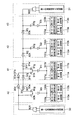
図1は、本実施形態に係る半導体装置1における電源系統のレイアウト図である。この図1に示すように、本実施形態に係る半導体装置1は、複数の電源系統を有している。具体的には、電源10から電力の供給を受ける、電源回路20〜26と、電源回路20から電力の供給を受ける第1の発振信号生成回路30と、電源回路21〜24から、それぞれ電力の供給を受ける第1乃至第4の回路部40〜43と、電源回路25から電力の供給を受ける第2の発振信号生成回路31と、電源回路26から電力の供給を受ける制御回路50とを備えて構成されている。
FIG. 1 is a layout diagram of a power supply system in a
電源10は、半導体装置1の外部に設けられた電力供給源であり、例えば、アルカリマンガン乾電池等の一次電池、リチウムイオン電池等の二次電池、直流変換をした家庭用電源等により構成される。
The
電源回路20〜26は、電源10から供給された電力を安定化させ、また必要に応じて電圧変換等を行い、第1及び第2の発振信号生成回路30、31、第1乃至第4の回路部40〜43、制御回路50にそれぞれ供給する電源系統を形成する。また、電源回路20〜26は、異なる電源系統に設けられた各回路で発生する信号の影響が相互に及ばないように遮断する役割を有している。例えば、第1の回路部40の動作に起因して、電源回路21の電源系統の電圧にふらつきが生じた場合でも、他の電源回路の電源系統の電圧にはその影響が及ばないように構成されている。
The
第1及び第2の発振信号生成回路30、31は、第1乃至第4の回路部40〜43で使用される発振信号を生成する。具体的には、第1の発振信号生成回路30は、第1の周波数の第1の発振信号を生成し、第1乃至第4の回路部40〜43に供給する。第2の発振信号生成回路31は、第1の周波数とは異なる第2の周波数の第2の発振信号を生成し、第1乃至第4の回路部40〜43に供給する。
The first and second oscillation
制御回路50は、半導体装置1内で行われる種々の動作の全体的な制御を行う。本実施形態においては、特に、第1及び第2の発振信号生成回路30、31の制御を行うための制御信号を生成し、また、第1乃至第4の回路部40〜43の制御を行うための制御信号を生成する。
The
半導体装置1が通信用に用いられる場合、このように電源系統を複数設けて、異なる系統の間で信号の干渉を低減することが一般的に行われている。なお電源系統の数は、半導体装置1の仕様や通信規格等に応じて様々である。
When the
図2は、本実施形態に係る半導体装置1における回路構成の一部を説明する回路図とブロック図である。
FIG. 2 is a circuit diagram and a block diagram illustrating a part of the circuit configuration in the
この図2に示すように、第1の発振信号生成回路30は第1の周波数の第1の発振信号を生成して、第1の回路部40に出力する。本実施形態においては、例えば、第1の周波数は2GHzであり、2GHzの発振信号が第1の回路部40に入力される。
As shown in FIG. 2, the first oscillation
一方、第2の発振信号生成回路31は第2の周波数の第2の発振信号を生成して、第4の回路部43に出力する。本実施形態においては、例えば、第2の周波数は5GHzであり、5GHzの発振信号が第4の回路部43に入力される。なお、2GHz、5GHzは、第1の周波数と第2の周波数に関する単なる例示であり、例えば、第1の周波数が5.50GHzであり、第2の周波数が5.52GHzのように、第1の発振信号の第1の周波数と第2の発振信号の第2の周波数が、さらに近接している場合も本実施形態においては想定の範囲である。
On the other hand, the second oscillation
第1の回路部40は、IQ信号発生器60と、送信器70と、受信器80とを備えている。IQ信号発生器60は、変調及び復調に用いる、同相位相成分であるI信号と直交位相成分であるQ信号とを生成する回路である。
The
送信器70は、IQ信号発生器60で生成されたI信号とQ信号とを用いて、送信信号を直交変調して送信波を生成する回路である。生成された送信波は、図示しないアンテナ等から出力される。
The
受信器80は、アンテナ等を介して受信された受信波を、IQ信号発生器60で生成されたI信号とQ信号とを用いて直交復調して、受信信号を生成する回路である。生成された受信信号は、半導体装置1において種々の処理に用いられる。
The
これらIQ信号発生器60と送信器70と受信器80は、本実施形態における第1の回路部40の第1の処理部の一例であり、電源回路21の電源系統から供給された電力により動作する。また、第1の回路部40は、IQ信号発生器60と送信器70と受信器80以外にも、他の処理を行う回路を第1の処理部として備えていてもよい。
The
この第1の回路部40と同様に、第2の回路部41は第2の処理部としてIQ信号発生器61と送信器71と受信器81とを備えており、第3の回路部42は第3の処理部としてIQ信号発生器62と送信器72と受信器82とを備えており、第4の回路部43は第4の処理部としてIQ信号発生器63と送信器73と受信器83とを備えている。
Similarly to the
さらに、第1の回路部40は、上記のIQ信号発生器60と送信器70と受信器80に加えて、キャパシタ90aと、バッファ90bと、キャパシタ90cと、バッファ90dと、キャパシタ90eと、バッファ90fと、キャパシタ90gと、キャパシタ90hと、バッファ90iとを備えている。
Further, the
第1の発振信号生成回路30における第1の発振信号の出力は、キャパシタ90aを介して、バッファ90bに接続されている。このため、バッファ90bには、第1の発振信号生成回路30から、第1の周波数の第1の発振信号が入力される。ここで、本実施形態において「入力される」とは、信号が他の素子等を介して間接的に入力される場合と、信号が他の素子等を介さずに直接的に入力される場合の双方を含む意味で用いる。
The output of the first oscillation signal in the first oscillation
バッファ90bの出力は、キャパシタ90cを介してバッファ90dの入力に接続されており、また、キャパシタ90hを介して、バッファ90iの入力に接続されている。さらに、バッファ90fの出力も、キャパシタ90gを介して、バッファ90iの入力に接続されている。そして、バッファ90iの出力はIQ信号発生器60に入力されている。
The output of the
バッファ90b、90d、90fは、それぞれ、制御信号に基づいて、入力された信号を出力するか否かを個別に制御可能なバッファである。これらの制御信号は、図1に示した制御回路50で個別に生成され、それぞれ、バッファ90b、90d、90fに入力される。すなわち、入力された信号を出力する指示の制御信号が入力されているバッファ90b、90d、90fについては、入力された発振信号をバッファリングして出力する。一方、入力された信号を出力しない指示の制御信号が入力されているバッファ90b、90d、90fについては、入力された制御信号は出力しない。
The
バッファ90iは、別個の制御信号に基づいて、入力された信号を出力するか否かを個別に制御可能なバッファである必要はない。すなわち、入力された信号を、非選択的に、出力するバッファで足りる。但し、バッファ90b、90d、90fと同様に、バッファ90iを、別個の制御信号に基づいて、入力された信号を出力するか否かを個別に制御可能なバッファで構成してもよい。この場合、バッファ90iには、動作中は定常的に、入力された信号を出力する指示の制御信号が入力されていることとなる。
The
なお、バッファ90b、90d、90f、90iは、IQ信号発生器60と送信器70と受信器80と同様に、電源回路21の電源系統である第1の電源系統から供給された電力により動作する。
The
第2の回路部41も、上述したIQ信号発生器61と送信器71と受信器81に加えて、キャパシタ91aと、バッファ91bと、キャパシタ91cと、バッファ91dと、キャパシタ91eと、バッファ91fと、キャパシタ91gと、キャパシタ91hと、バッファ91iと、キャパシタ91jと、バッファ91kとを備えている。
The
第2の回路部41におけるキャパシタ91aとバッファ91bとキャパシタ91cとバッファ91dとキャパシタ91eとバッファ91fとキャパシタ91gとキャパシタ91hとバッファ91iは、上述した第1の回路部40におけるキャパシタ90aとバッファ90bとキャパシタ90cとバッファ90dとキャパシタ90eとバッファ90fとキャパシタ90gとキャパシタ90hとバッファ90iに、それぞれ、対応している。
The
そしてさらに、バッファ91fの出力は、キャパシタ91gを介してバッファ91iの入力に接続されているのに加えて、キャパシタ91jを介して、バッファ91kの入力に接続されている。バッファ91kは、バッファ91b、91d、91fと同様に、制御信号に基づいて、入力された信号を出力するか否かを個別に制御可能なバッファである。
Further, the output of the
第1の回路部40のバッファ90dの出力と、第1の回路部40のキャパシタ90eを介したバッファ90fの入力と、第2の回路部41のキャパシタ91aを介したバッファ91bの入力と、第2の回路部41のバッファ91kの出力とは、共通に接続されている。すなわち、バッファ90dとバッファ91bとの間の伝送路と、バッファ91kとバッファ90fとの間の伝送路は、共通化されて1本になっている。ここで、第1の回路部40と第2の回路部41との間で遣り取りする発振信号が単相信号の場合には、1本の伝送路における物理的な信号配線は1本であるが、第1の回路部40と第2の回路部41との間で遣り取りする発振信号が差動信号の場合には、1本の伝送路における物理的な信号配線は2本である。
The output of the
なお、バッファ91b、91d、91f、91k、91iは、IQ信号発生器61と送信器71と受信器81と同様に、電源回路22の電源系統である第2の電源系統から供給された電力により動作する。
The
第3の回路部42は、第2の回路部41と同様の構成であり、上述したIQ信号発生器62と送信器72と受信器82に加えて、キャパシタ92aと、バッファ92bと、キャパシタ92cと、バッファ92dと、キャパシタ92eと、バッファ92fと、キャパシタ92gと、キャパシタ92hと、バッファ92iと、キャパシタ92jと、バッファ92kとを備えている。
The
第3の回路部42におけるキャパシタ92aとバッファ92bとキャパシタ92cとバッファ92dとキャパシタ92eとバッファ92fとキャパシタ92gとキャパシタ92hとバッファ92iとキャパシタ92jとバッファ92kは、上述した第2の回路部41におけるキャパシタ91aとバッファ91bとキャパシタ91cとバッファ91dとキャパシタ91eとバッファ91fとキャパシタ91gとキャパシタ91hとバッファ91iキャパシタ91jとバッファ91kに、それぞれ、対応している。
The
また、第2の回路部41のバッファ91dの出力と、第2の回路部41のキャパシタ91eを介したバッファ91fの入力と、第3の回路部42のキャパシタ92aを介したバッファ92bの入力と、第3の回路部42のバッファ92kの出力とは、共通に接続されている。すなわち、バッファ91dとバッファ92bとの間の伝送路と、バッファ92kとバッファ91fとの間の伝送路は、共通化されて1本になっている。
The output of the
なお、バッファ92b、92d、92f、92k、92iは、IQ信号発生器62と送信器72と受信器82と同様に、電源回路23の電源系統である第3の電源系統から供給された電力により動作する。
The
第4の回路部43は、上述したIQ信号発生器63と送信器73と受信器83に加えて、キャパシタ93aと、バッファ93bと、キャパシタ93eと、バッファ93fと、キャパシタ93gと、キャパシタ93hと、バッファ93iと、キャパシタ93jと、バッファ93kとを備えている。
The
第4の回路部43におけるキャパシタ93aとバッファ93bとキャパシタ93eとバッファ93fとキャパシタ93gとキャパシタ93hとバッファ93iとキャパシタ93jとバッファ93kは、上述した第3の回路部42におけるキャパシタ92aとバッファ92bとキャパシタ92eとバッファ92fとキャパシタ92gとキャパシタ92hとバッファ92iとキャパシタ92jとバッファ92kに、それぞれ、対応している。
The
但し、第2の発振信号生成回路31における第2の発振信号の出力が、キャパシタ93eを介して、バッファ93fの入力に接続されている。このため、バッファ93fには、第2の発振信号生成回路31から、第2の周波数の第2の発振信号が入力される。
However, the output of the second oscillation signal in the second oscillation
また、第3の回路部42のバッファ92dの出力と、第3の回路部42のキャパシタ92eを介したバッファ92fの入力と、第4の回路部43のキャパシタ93aを介したバッファ93bの入力と、第4の回路部43のバッファ93kの出力とは、共通に接続されている。すなわち、バッファ92dとバッファ93bとの間の伝送路と、バッファ93kとバッファ92fとの間の伝送路は、共通化されて1本になっている。
The output of the
なお、バッファ93b、93f、93k、93iは、IQ信号発生器63と送信器73と受信器83と同様に、電源回路24の電源系統である第4の電源系統から供給された電力により動作する。
The
なお、各バッファの入力にはキャパシタが接続されているが、これは、キャパシタにより、信号の直流成分を遮断するために設けられている。すなわち、第1の発振信号及び第2の発振信号の直流成分は、各キャパシタにより遮断される。 A capacitor is connected to the input of each buffer, which is provided to cut off the DC component of the signal by the capacitor. That is, the DC components of the first oscillation signal and the second oscillation signal are cut off by each capacitor.
以上が本実施形態に係る半導体装置1の回路構成であるが、次に、この半導体装置1の動作について説明する。
The above is the circuit configuration of the
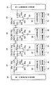
図3は、第2の発振信号生成回路31により生成された第2の発振信号を、第1乃至第4の回路部40〜43に供給する場合の回路状態を説明するための図である。本実施形態においては、この状態を第1のモードと言うこととする。
FIG. 3 is a diagram for explaining a circuit state when the second oscillation signal generated by the second oscillation
この図3に示すように、第1のモードにおいては、バッファ90b、90d、91b、91d、92b、92d、93dに、入力された信号を出力しない指示の制御信号が入力されており、バッファ90f、91k、91f、92k、92f、93k、93fに、入力された信号を出力する指示の制御信号が入力されている。
As shown in FIG. 3, in the first mode, a control signal of an instruction not to output the input signal is input to
このため、第1の発振信号生成回路30で生成された第1の発振信号は、バッファ90bで遮断され、第1乃至第4の回路部40〜43のいずれにも供給されない。一方、第2の発振信号生成回路31で生成された第2の発振信号は、バッファ93f、93k、92f、92k、91f、91k、90fを順に経由して、第1乃至第4の回路部40〜43のIQ信号発生器60〜63に供給される。
Therefore, the first oscillation signal generated by the first oscillation
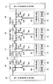
図4は、第1の発振信号生成回路30により生成された第1の発振信号を、第1の回路部40に供給し、第2の発振信号生成回路31により生成された第2の発振信号を、第2乃至第4の回路部41〜43に供給する場合の回路状態を説明するための図である。本実施形態においては、この状態を第2のモードと言うこととする。
FIG. 4 shows a case where the first oscillation signal generated by the first oscillation
この図4に示すように、第2のモードにおいては、バッファ90d、90f、91b、91d、91k、92b、92d、93dに、入力された信号を出力しない指示の制御信号が入力されており、バッファ90b、91f、92k、92f、93k、93fに、入力された信号を出力する指示の制御信号が入力されている。
As shown in FIG. 4, in the second mode, a control signal for instructing not to output the input signal is input to the
このため、第1の発振信号生成回路30で生成された第1の発振信号は、第1の回路部40のIQ信号発生器60に供給されるが、バッファ90dで遮断される。一方、第2の発振信号生成回路31で生成された第2の発振信号は、バッファ93f、93k、92f、92k、91fを順に経由して、第2乃至第4の回路部41〜43のIQ信号発生器61〜63に供給されるが、バッファ91kで遮断される。
Therefore, the first oscillation signal generated by the first oscillation
このとき、領域A1にあるバッファ90d、90f、91b、91kは、いずれも、入力された信号を出力しない不活性な状態にある。つまり、第1の回路部40と第2の回路部41との間は、電源系統が異なるバッファ90dとバッファ91bの2つのバッファで分離され、また、電源系統が異なるバッファ90fとバッファ91kの2つのバッファで分離されることとなる。このため、第1の発振信号と第2の発振信号との間のアイソレーションを高く確保することができ、クロストークの発生が抑制される。
At this time, the
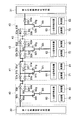
図5は、第1の発振信号生成回路30により生成された第1の発振信号を、第1乃至第2の回路部40〜41に供給し、第2の発振信号生成回路31により生成された第2の発振信号を、第3乃至第4の回路部42〜43に供給する場合の回路状態を説明するための図である。本実施形態においては、この状態を第3のモードと言うこととする。
FIG. 5 shows a case where the first oscillation signal generated by the first oscillation
この図5に示すように、第3のモードにおいては、バッファ90f、91d、91f、91k、92b、92d、92k、93bに、入力された信号を出力しない指示の制御信号が入力されており、バッファ90b、90d、91b、92f、93k、93fに、入力された信号を出力する指示の制御信号が入力されている。
As shown in FIG. 5, in the third mode, a control signal of an instruction not to output the input signal is input to the
このため、第1の発振信号生成回路30で生成された第1の発振信号は、第1及び第2の回路部40〜41のIQ信号発生器60〜61に供給されるが、バッファ91dで遮断される。一方、第2の発振信号生成回路31で生成された第2の発振信号は、バッファ93f、93k、92fを順に経由して、第3乃至第4の回路部42〜43のIQ信号発生器62〜63に供給されるが、バッファ92kで遮断される。
Therefore, the first oscillation signal generated by the first oscillation
このとき、領域A2にあるバッファ91d、91f、92b、92kは、いずれも、入力された信号を出力しない不活性な状態にある。つまり、第2の回路部41と第3の回路部42との間は、電源系統が異なるバッファ91dとバッファ92bの2つのバッファで分離され、また、電源系統が異なるバッファ91fとバッファ92kの2つのバッファで分離されることとなる。このため、第1の発振信号と第2の発振信号との間のアイソレーションを高く確保することができ、クロストークの発生が抑制される。
At this time, the
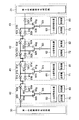
図6は、第1の発振信号生成回路30により生成された第1の発振信号を、第1乃至第3の回路部40〜42に供給し、第2の発振信号生成回路31により生成された第2の発振信号を、第4の回路部43に供給する場合の回路状態を説明するための図である。本実施形態においては、この状態を第4のモードと言うこととする。
FIG. 6 shows a case where the first oscillation signal generated by the first oscillation
この図6に示すように、第4のモードにおいては、バッファ90f、91f、91k、92d、92f、92k、93b、93kに、入力された信号を出力しない指示の制御信号が入力されており、バッファ90b、90d、91b、91d、92b、93fに、入力された信号を出力する指示の制御信号が入力されている。
As shown in FIG. 6, in the fourth mode, a control signal for instructing not to output the input signal is input to the
このため、第1の発振信号生成回路30で生成された第1の発振信号は、第1乃至第3の回路部40〜42のIQ信号発生器60〜62に供給されるが、バッファ92dで遮断される。一方、第2の発振信号生成回路31で生成された第2の発振信号は、バッファ93fを経由して、第4の回路部43のIQ信号発生器63に供給されるが、バッファ93kで遮断される。
For this reason, the first oscillation signal generated by the first oscillation
このとき、領域A3にあるバッファ92d、92f、93b、93kは、いずれも、入力された信号を出力しない不活性な状態にある。つまり、第3の回路部42と第4の回路部43との間は、電源系統が異なるバッファ92dとバッファ93bの2つのバッファで分離され、また、電源系統が異なるバッファ92fとバッファ93kの2つのバッファで分離されることとなる。このため、第1の発振信号と第2の発振信号との間のアイソレーションを高く確保することができ、クロストークの発生が抑制される。
At this time, the
図7は、第1の発振信号生成回路30により生成された第1の発振信号を、第1乃至第4の回路部40〜43に供給する場合の回路状態を説明するための図である。本実施形態においては、この状態を第5のモードと言うこととする。
FIG. 7 is a diagram for explaining a circuit state when the first oscillation signal generated by the first oscillation
この図7に示すように、第5のモードにおいては、バッファ90f、91f、91k、92f、92k、93f、93kに、入力された信号を出力しない指示の制御信号が入力されており、バッファ90b、90d、91b、91d、92b、92d、93bに、入力された信号を出力する指示の制御信号が入力されている。
As shown in FIG. 7, in the fifth mode, a control signal indicating that the input signal is not output is input to the
このため、第1の発振信号生成回路30で生成された第1の発振信号は、第1乃至第4の回路部40〜43のIQ信号発生器60〜63に供給される。一方、第2の発振信号生成回路31で生成された第2の発振信号は、バッファ93fで遮断され、第1乃至第4の回路部40〜43のいずれにも供給されない。
Therefore, the first oscillation signal generated by the first oscillation
次に、図8に基づいて、入力された信号を出力するか否かを個別に制御可能なバッファの回路構成について説明する。図8は、制御信号に基づいて、入力された信号を出力するか否かを個別に制御可能なバッファの具体的な回路構成の一例を示す図である。 Next, a circuit configuration of a buffer that can individually control whether to output an input signal will be described with reference to FIG. FIG. 8 is a diagram illustrating an example of a specific circuit configuration of a buffer that can individually control whether to output an input signal based on a control signal.
この図8に示すように、バッファは、PチャネルMOSトランジスタP1、P2、P3と、NチャネルMOSトランジスタN1、N2、N3と、抵抗R1と、インバータ回路IN1とを備えて構成されている。 As shown in FIG. 8, the buffer includes P-channel MOS transistors P1, P2, P3, N-channel MOS transistors N1, N2, N3, a resistor R1, and an inverter circuit IN1.
PチャネルMOSトランジスタP1の制御端子と、NチャネルMOSトランジスタN1の制御端子と、抵抗R1の一端は、それぞれ入力端子に接続されており、この入力端子から入力信号INが入力される。PチャネルMOSトランジスタP1の第1端子は第1電源Vddに接続されており、NチャネルMOSトランジスタN1の第1端子は第2電源Vccに接続されている。 The control terminal of the P-channel MOS transistor P1, the control terminal of the N-channel MOS transistor N1, and one end of the resistor R1 are connected to input terminals, respectively, from which the input signal IN is input. The first terminal of the P-channel MOS transistor P1 is connected to the first power supply Vdd, and the first terminal of the N-channel MOS transistor N1 is connected to the second power supply Vcc.
第1電源Vddと第2電源Vccとの間には、さらに、PチャネルMOSトランジスタP2、P3と、NチャネルMOSトランジスタN2、N3とが、直列的に接続されている。PチャネルMOSトランジスタP3の制御端子とNチャネルMOSトランジスタN2の制御端子は、PチャネルMOSトランジスタP1の第2端子とNチャネルMOSトランジスタN1の第2端子と抵抗R1の他端に、共通に接続されている。 Further, P-channel MOS transistors P2 and P3 and N-channel MOS transistors N2 and N3 are connected in series between the first power supply Vdd and the second power supply Vcc. The control terminal of the P-channel MOS transistor P3 and the control terminal of the N-channel MOS transistor N2 are commonly connected to the second terminal of the P-channel MOS transistor P1, the second terminal of the N-channel MOS transistor N1, and the other end of the resistor R1. ing.
制御回路50で生成された制御信号Enableは、NチャネルMOSトランジスタN3の制御端子に入力される。また、制御信号Enableは、インバータ回路IN1にも入力され、反転された上で、PチャネルMOSトランジスタP2の制御端子に入力される。
The control signal Enable generated by the
このため、ハイレベルの制御信号Enableが入力されている場合は、PチャネルMOSトランジスタP2とNチャネルMOSトランジスタN3とが、オン状態となり、このバッファは、入力された信号INをバッファリングして、出力信号OUTとして出力する回路となる。一方、ローレベルの制御信号Enableが入力されている場合は、PチャネルMOSトランジスタP2とNチャネルMOSトランジスタN3とが、オフ状態となり、このバッファは、入力された信号を出力しない回路となる。つまり、ハイレベルの制御信号が、入力された信号を出力する指示の制御信号となり、ローレベルの制御信号が、入力された信号を出力しない指示の制御信号となる。 Therefore, when the high-level control signal Enable is input, the P-channel MOS transistor P2 and the N-channel MOS transistor N3 are turned on, and this buffer buffers the input signal IN. A circuit that outputs the output signal OUT. On the other hand, when the low-level control signal Enable is input, the P-channel MOS transistor P2 and the N-channel MOS transistor N3 are turned off, and this buffer is a circuit that does not output the input signal. That is, the high-level control signal is a control signal for instructing to output the input signal, and the low-level control signal is a control signal for not outputting the input signal.
本実施形態においては、入力信号INと出力信号OUTは、第1の発振信号と第2の発振信号のいずれかとなる。また、第1電源Vddと第2電源Vccとが、図1の電源回路20〜26から供給される。より具体的には、第1の回路部40にあるバッファ90b、90d、90fには、電源回路21から第1電源Vddと第2電源Vccが供給され、第2の回路部41にあるバッファ91b、91d、91f、91kには、電源回路22から第1電源Vddと第2電源Vccが供給され、第3の回路部42にあるバッファ92b、92d、92f、92kには、電源回路23から第1電源Vddと第2電源Vccが供給され、第4の回路部43にあるバッファ93b、93f、93kには、電源回路24から第1電源Vddと第2電源Vccが供給される。
In the present embodiment, the input signal IN and the output signal OUT are either the first oscillation signal or the second oscillation signal. The first power supply Vdd and the second power supply Vcc are supplied from the
以上のように、本実施形態に係る半導体装置1によれば、第1の発振信号又は第2の発振信号をバッファリングするバッファを、第1乃至第4の回路部40〜43のそれぞれに供給される電力により動作させることとした。さらに、第1乃至第4の回路部40〜43のそれぞれの間を、2つの不活性なバッファで分離することとした。このため、第1の発振信号と第2の発振信号との間のアイソレーションを高く確保することができ、クロストークの発生を抑制することができる。
As described above, according to the
また、第1乃至第4の回路部40〜43のぞれぞれの間を、1本の伝送路を用いて、第1の発振信号と第2の発振信号を遣り取りすることとしたので、レイアウト面積の抑制を図ることができる。特に、第1の発振信号の周波数と第2の発振信号の周波数が近接している場合には、2つの信号の伝送路を可能な限り離してレイアウトをする必要があるため、レイアウト面積の増大を招く可能性があるが、本実施形態のように1本の伝送路として共通化することにより、レイアウト面積の削減を図ることができる。
Further, since the first oscillation signal and the second oscillation signal are exchanged between each of the first to
図9は、本実施形態に係る半導体装置1を機能的に説明するためのブロック回路図である。この図9に示すように、半導体装置1は、択一的な経路で第1乃至第4の回路部40〜43に辿り着いた第1の発振信号又は第2の発振信号が、交わることなく、IQ信号発生器60〜63に供給される機能を有するととらえることができる。このような機能を実現するために、第1乃至第4の回路部40〜43は、それぞれ、選択回路SL1、SL2、SL3と、バッファBF1、BF2とを備えていると言える。
FIG. 9 is a block circuit diagram for functionally explaining the
選択回路SL1、SL2、SL3は、入力された第1の発振信号と第2の発振信号のうち一方を出力する回路であり、いずれの発振信号を出力するのかは、制御回路50から入力される制御信号に基づいて切り替えられる。バッファBF1、BF2は、それぞれ、入力された第1の発振信号又は第2の発振信号をバッファリングして出力する回路である。
The selection circuits SL1, SL2, and SL3 are circuits that output one of the input first oscillation signal and the second oscillation signal. Which of the oscillation signals is output is input from the
第1の発振信号生成回路30により生成された第1の発振信号と、第2の発振信号生成回路31により生成された第2の発振信号とは、選択回路SL1、SL2の切り替え制御により、択一的に形成された経路で、第1乃至第4の回路部40〜43に辿り着き、選択回路SL3の切り替え制御により、交わることなく、IQ信号発生器60〜63に供給される。つまり、選択回路SL1、SL2、SL3を制御信号によって制御することにより、第1の発振信号と第2の発振信号は、交わることなく、IQ信号発生器60〜63に供給されるのである。
The first oscillation signal generated by the first oscillation
なお、図10に示すように、本実施形態に係る半導体装置1は、第1乃至第4の回路部40〜43のそれぞれの間の伝送路を2本にすることも可能である。すなわち、第1の発振信号の伝送路と、第2の発振信号の伝送路とを別個に設けるようにしてもよい。この場合、伝送路のレイアウト面積はその分、増大するが、第1の発振信号と第2の発振信号を、第1乃至第4の回路部40〜43の任意の組み合わせの回路部に供給することができるようになる。例えば、第1の回路部40と第3の回路部42に第1の発振信号生成回路30から第1の発振信号を供給し、第2の回路部41と第4の回路部43に第2の発振信号生成回路31から第2の発振信号を供給することができるようになる。
As shown in FIG. 10, the
また、図11に示すように、本実施形態に係る半導体装置1は、キャパシタ90aとバッファ90bを第1の発振信号生成回路30の出力近傍に設け、第1の発振信号生成回路30と同じ電源回路20の電源系統から得た電力に基づいてバッファ90bが動作し、且つ、キャパシタ93eとバッファ93fを第2の発振信号生成回路31の出力近傍に設け、第2の発振信号生成回路31と同じ電源回路25の電源系統から得た電力に基づいてバッファ93fが動作するようにしてもよい。
As shown in FIG. 11, in the
〔第2実施形態〕
第2実施形態は、上述した第1実施形態を変形して、第1の発振信号生成回路30が第1の発振信号と第2の発振信号を生成して、第1及び第2の回路部40〜41に供給し得るように構成し、第2の発振信号生成回路31も第1の発振信号と第2の発振信号を生成して、第1乃至第4の回路部40〜43に供給し得るように構成することにより、レイアウト面積の削減を実現している。以下、上述した第1実施形態と異なる部分を説明する。
[Second embodiment]
The second embodiment is a modification of the first embodiment described above, in which the first oscillation
図12は、本実施形態に係る半導体装置1における回路構成の一部を説明する回路図とブロック図であり、上述した第1実施形態の図2に対応する図である。
FIG. 12 is a circuit diagram and a block diagram illustrating a part of the circuit configuration of the
この図12に示すように、本実施形態における第1の発振信号生成回路30は、第1の周波数の第1の発振信号と、第2の周波数の第2の発振信号の双方を生成し、選択回路MUX1に出力する。上述した第1実施形態と同様に、例えば、第1の周波数は2GHzであり、第2の周波数は5GHzである。
As shown in FIG. 12, the first oscillation
選択回路MUX1には、図1に示した制御回路50から選択用の制御信号が入力され、この制御信号に基づいて、選択回路MUX1は、第1の発振信号と第2の発振信号とのうちのいずれかを出力するか、或いは、選択回路MUX1は、入力された第1の発振信号と第2の発振信号のいずれも出力しない。この選択回路MUX1は、第1の発振信号生成回路30と同様に、電源回路20の電源系統から供給された電力により動作する。
A selection control signal from the
第2の発振信号生成回路31も、第1の周波数の第1の発振信号と、第2の周波数の第2の発振信号の双方を生成し、選択回路MUX2に出力する。第1の発振信号生成回路30と同様に、例えば、第1の周波数は2GHzであり、第2の周波数は5GHzである。なお、上述した第1実施形態と同様に、2GHz、5GHzは、第1の周波数と第2の周波数に関する単なる例示であり、例えば、第1の周波数が5.50GHzであり、第2の周波数が5.52GHzのように、第1の発振信号の第1の周波数と第2の発振信号の第2の周波数が、さらに近接している場合も本実施形態においては想定の範囲である。
The second oscillation
選択回路MUX2にも、図1に示した制御回路50から選択用の制御信号が入力され、この制御信号に基づいて、選択回路MUX2は、第2の発振信号と第2の発振信号のうちのいずれかを出力する。この選択回路MUX2は、第2の発振信号生成回路31と同様に、電源回路25から供給された電力により動作する。
The selection control signal from the
選択回路MUX1から出力された第1の発振信号又は第2の発振信号は、第1の回路部40に供給される。具体的には、キャパシタ90cを介してバッファ90dに入力され、キャパシタ90hを介してバッファ90iに入力される。
The first oscillation signal or the second oscillation signal output from the selection circuit MUX1 is supplied to the
第1の回路部40は、第1のIQ信号発生器100aと、第2のIQ信号発生器100bと、第1の送受信器110aと、第2の送受信器110bとを備えており、バッファ90iから第1の発振信号又は第2の発振信号が入力される。すなわち、バッファ90iから第1の発振信号が入力されている場合には、第1のIQ信号発生器100aが動作し、第1の送受信器110aを用いて送受信が行われる。一方、バッファ90iから第2の発振信号が入力されている場合には、第2のIQ信号発生器100bが動作し、第2の送受信器110bを用いて送受信が行われる。
The
なお、図12においては、「送信器」と「受信器」を併合して「送受信器」として1つのブロックで表現しているが、「送信器」と「受信器」とを別個のブロックとして表現している第1実施形態と機能上は同じである。 In FIG. 12, the “transmitter” and the “receiver” are combined and expressed as one block as a “transmitter / receiver”, but the “transmitter” and the “receiver” are separated as separate blocks. The functions are the same as those of the first embodiment.
同様に、第2乃至第4の回路部41〜43のバッファ91i、92i、93iからは、それぞれ、第1の発振信号又は第2の発振信号が出力され、第1の発振信号が出力されている場合には、第1のIQ信号発生器101a、102a、103aが動作し、第1の送受信器111a、112a、113aを用いて送受信が行われ、第2の発振信号が出力されている場合には、第2のIQ信号発生器101b、102b、103bが動作し、第2の送受信器111b、112b、113bを用いて送受信が行われる。
Similarly, the
但し、第1の回路部40と第2の回路部41には、第1の発振信号生成回路30と第2の発振信号生成回路31の双方から、第1の発振信号又は第2の発振信号が供給され得るのに対し、第3の回路部42と第4の回路部43には、第2の発振信号生成回路31から第1の発振信号又は第2の発振信号が供給され得るが、第1の発振信号生成回路30からは第1の発振信号も第2の発振信号も供給され得ない構成となっている。
However, the
また、上述した第1実施形態と異なり、第1の回路部40と第2の回路部41との間は、2本の伝送路が設けられている。すなわち、バッファ90dとバッファ91bとの間に1本の専用の伝送路が設けられており、バッファ90fとバッファ91kとの間に1本の専用の伝送路が設けられている。
Further, unlike the above-described first embodiment, two transmission paths are provided between the
さらに、第4の回路部43に設けられたバッファ93kは、入力された第1の発振信号又は第2の発振信号を非選択的に出力するので、別個の制御信号に基づいて、入力された信号を出力するか否かを制御可能なバッファではない。但し、バッファ93kは、上述した第1実施形態と同様に、別個の制御信号に基づいて、入力された信号を出力するか否かを制御可能なバッファで構成することも可能である。この場合、バッファ93kには、動作中は定常的に、入力された信号を出力する指示の制御信号が入力されることとなる。
Further, the
以上が本実施形態に係る半導体装置1の回路構成であるが、次に、この半導体装置1の動作について説明する。
The above is the circuit configuration of the
<第1の発振信号×4、又は、第2の発振信号×4>
図13は、第1の発振信号を第1乃至第4の回路部40〜43に供給する場合、又は、第2の発振信号を第1乃至第4の回路部40〜43に供給する場合における、回路状態を説明するための図である。本実施形態においては、この状態を第1のモードと言うこととする。
<First oscillation signal × 4 or second oscillation signal × 4>
FIG. 13 illustrates the case where the first oscillation signal is supplied to the first to
この図13に示すように、第1のモードでは、バッファ90d、91bに、入力された信号を出力しない指示の制御信号が入力されており、バッファ90f、91k、91f、92kに、入力された信号を出力する指示の制御信号が入力されている。また、選択回路MUX1には、第1の発振信号と第2の発振信号のいずれも出力しない制御信号が入力されている。
As shown in FIG. 13, in the first mode, a control signal instructing not to output an input signal is input to
このため、選択回路MUX2に第1の発振信号を選択する制御信号が入力されている場合には、バッファ93k、92k、91f、91k、90fを順に経由して、第1乃至第4の回路部40〜43に、第1の発振信号が供給される。
Therefore, when a control signal for selecting the first oscillation signal is input to the selection circuit MUX2, the first to fourth circuit units are sequentially passed through the
一方、選択回路MUX2に第2の発振信号を選択する制御信号が入力されている場合には、バッファ93k、92k、91f、91k、90fを順に経由して、第1乃至第4の回路部40〜43に、第2の発振信号が供給される。
On the other hand, when the control signal for selecting the second oscillation signal is input to the selection circuit MUX2, the first to
<第1の発振信号×1+第2の発振信号×3、又は、第1の発振信号×3+第2の発振信号×1>
図14は、第1の発振信号を第1の回路部40に供給し、且つ、第2の発振信号を第2乃至第4の回路部41〜43に供給する場合、又は、第2の発振信号を第1の回路部40に供給し、第1の発振信号を第2乃至第4の回路部41〜43に供給する場合における、回路状態を説明するための図である。本実施形態においては、この状態を第2のモードと言うこととする。
<First oscillation signal × 1 + second oscillation signal × 3, or first oscillation signal × 3 + second oscillation signal × 1>
FIG. 14 illustrates a case where the first oscillation signal is supplied to the
この図14に示すように、第2のモードでは、バッファ90d、90f、91b、91kに、入力された信号を出力しない指示の制御信号が入力されており、バッファ91f、92kに、入力された信号を出力する指示の制御信号が入力されている。
As shown in FIG. 14, in the second mode, a control signal instructing not to output an input signal is input to
このため、選択回路MUX1に第1の発振信号を選択する制御信号が入力され、且つ、選択回路MUX2に第2の発振信号を選択する制御信号が入力されている場合には、選択回路MUX1から、第1の回路部40に第1の発振信号が供給され、選択回路MUX2から、バッファ93k、92k、91fを順に経由して、第2乃至第4の回路部41〜43に、第2の発振信号が供給される。
Therefore, when the control signal for selecting the first oscillation signal is input to the selection circuit MUX1 and the control signal for selecting the second oscillation signal is input to the selection circuit MUX2, the selection circuit MUX1 outputs , The first oscillation signal is supplied to the
一方、選択回路MUX1に第2の発振信号を選択する制御信号が入力され、且つ、選択回路MUX2に第1の発振信号を選択する制御信号が入力されている場合には、選択回路MUX1から、第1の回路部40に第2の発振信号が供給され、選択回路MUX2から、バッファ93k、92k、91fを順に経由して、第2乃至第4の回路部41〜43に、第1の発振信号が供給される。
On the other hand, when the control signal for selecting the second oscillation signal is input to the selection circuit MUX1 and the control signal for selecting the first oscillation signal is input to the selection circuit MUX2, The second oscillation signal is supplied to the
このとき、領域A4にあるバッファ90d、90f、91b、91kは、いずれも、入力された信号を出力しない不活性な状態にある。つまり、第1の回路部40と第2の回路部41との間は、電源系統が異なるバッファ90dとバッファ91bの2つのバッファで分離され、また、電源系統が異なるバッファ90fとバッファ91kの2つのバッファで分離されることとなる。このため、第1の発振信号と第2の発振信号との間のアイソレーションを高く確保することができ、クロストークの発生が抑制される。
At this time, the
<第1の発振信号×2+第2の発振信号×2>
図15は、第1の発振信号を第1乃至第2の回路部40〜41に供給し、且つ、第2の発振信号を第3乃至第4の回路部42〜43に供給する場合、又は、第2の発振信号を第1乃至第2の回路部40〜41に供給し、第1の発振信号を第3乃至第4の回路部42〜43に供給する場合における、回路状態を説明するための図である。本実施形態においては、この状態を第3のモードと言うこととする。
<First oscillation signal × 2 + second oscillation signal × 2>
FIG. 15 illustrates a case where the first oscillation signal is supplied to the first to
この図15に示すように、第3のモードでは、バッファ90f、91f、91k、92kに、入力された信号を出力しない指示の制御信号が入力されており、バッファ90d、91bに、入力された信号を出力する指示の制御信号が入力されている。
As shown in FIG. 15, in the third mode, a control signal instructing not to output an input signal is input to
このため、選択回路MUX1に第1の発振信号を選択する制御信号が入力され、且つ、選択回路MUX2に第2の発振信号を選択する制御信号が入力されている場合には、選択回路MUX1から、第1乃至第2の回路部40〜41に第1の発振信号が供給され、選択回路MUX2から、バッファ93kを経由して、第3乃至第4の回路部42〜43に、第2の発振信号が供給される。
Therefore, when the control signal for selecting the first oscillation signal is input to the selection circuit MUX1 and the control signal for selecting the second oscillation signal is input to the selection circuit MUX2, the selection circuit MUX1 outputs The first oscillation signal is supplied to the first and
また結果的には同数とはなるが、選択回路MUX1に第2の発振信号を選択する制御信号が入力され、且つ、選択回路MUX2に第1の発振信号を選択する制御信号が入力されている場合には、選択回路MUX1から、第1乃至第2の回路部40〜41に第2の発振信号が供給され、選択回路MUX2から、バッファ93kを経由して、第3乃至第4の回路部42〜43に、第1の発振信号が供給される。
In addition, although the numbers are the same, a control signal for selecting the second oscillation signal is input to the selection circuit MUX1, and a control signal for selecting the first oscillation signal is input to the selection circuit MUX2. In this case, the second oscillation signal is supplied from the selection circuit MUX1 to the first and
このとき、領域A5にあるバッファ91f、92kは、いずれも、入力された信号を出力しない不活性な状態にある。つまり、第2の回路部41と第3の回路部42との間は、電源系統が異なるバッファ91fとバッファ92kの2つのバッファで分離されることとなる。このため、第1の発振信号と第2の発振信号との間のアイソレーションを高く確保することができ、クロストークの発生が抑制される。
At this time, the
以上のように、本実施形態に係る半導体装置1によれば、第1の発振信号又は第2の発振信号をバッファリングするバッファを、第1乃至第4の回路部40〜43のそれぞれに供給される電力により動作させることとした。さらに、第1乃至第3の回路部40〜42のそれぞれの間を、2つの不活性なバッファで分離することとした。このため、第1の発振信号と第2の発振信号との間のアイソレーションを高く確保することができ、クロストークの発生を抑制することができる。
As described above, according to the
また、第1の発振信号生成回路30と第2の発振信号生成回路31とが、ともに、第1の発振信号と第2の発振信号の双方を生成し、第1の発振信号生成回路30から選択的に第1乃至第2の回路部40〜41に第1の発振信号又は第2の発振信号を供給し、第2の発振信号生成回路31から選択的に第1乃至第4の回路部40〜43に第1の発振信号又は第2の発振信号を供給することしたので、バッファの活性状態/不活性状態を任意に組み合わせることにより、必要な数の回路部に、第1の発振信号を供給し、第2の発振信号を供給することができる。また、第2回路部41と第3回路部42との間の発振信号の伝送路を1本にすることができ、第3の回路部43と第4の回路部43との間の発振信号伝送路を1本にすることができるので、回路のレイアウト面積を削減することができる。
Further, the first oscillation
なお、図16に示すように、本実施形態に係る半導体装置1は、第1実施形態と同様に、第1の回路部40と第2の回路部41との間を、1本の伝送路で接続して、第1の発振信号又は第2の発振信号の遣り取りをすることもできる。これにより、さらなる回路面積の削減を図ることができる。
As shown in FIG. 16, the
また、図17に示すように、第1の発振信号生成回路30と同じ電源回路20の電源系統から選択回路MUX1に電力を供給するのではなく、第1の回路部40と同じ電源回路21の電源系統から選択回路MUX1に電力を供給するようにしてもよい。同様に、第2の発振信号生成回路31と同じ電源回路25の電源系統から選択回路MUX2に電力を供給するのではなく、第4の回路部43と同じ電源回路24の電源系統から選択回路MUX2に電力を供給するようにしてもよい。
Also, as shown in FIG. 17, power is not supplied to the selection circuit MUX <b> 1 from the power supply system of the same
以上、いくつかの実施形態を説明したが、これらの実施形態は、例としてのみ提示したものであり、発明の範囲を限定することを意図したものではない。本明細書で説明した新規な装置および方法は、その他の様々な形態で実施することができる。また、本明細書で説明した装置および方法の形態に対し、発明の要旨を逸脱しない範囲内で、種々の省略、置換、変更を行うことができる。添付の特許請求の範囲およびこれに均等な範囲は、発明の範囲や要旨に含まれるこのような形態や変形例を含むように意図されている。 While some embodiments have been described above, these embodiments have been presented by way of example only, and are not intended to limit the scope of the invention. The novel apparatus and method described herein can be implemented in various other forms. In addition, various omissions, substitutions, and changes can be made to the embodiments of the apparatus and method described in this specification without departing from the spirit of the invention. The appended claims and their equivalents are intended to cover such forms and modifications as fall within the scope and spirit of the invention.
10…電源、20〜26:電源回路、30:第1の発振信号生成回路、31:第2の発振信号生成回路、40〜43:第1乃至第4の回路部、50:制御回路、60〜63:IQ信号発生器、70〜73:送信器、80〜83:受信器、90a、90c、90e、90g、90h:キャパシタ、90b、90d、90f、90i:バッファ、91a、91c、91e、91g、91h、91j:キャパシタ、91b、91d、91f、91i、91k:バッファ、92a、92c、92e、92g、92h、92j:キャパシタ、92b、92d、92f、92i、92k:バッファ、93a、93e、93g、93h、93j:キャパシタ、93b、93f、93i、93k:バッファ 10 power supply, 20 to 26: power supply circuit, 30: first oscillation signal generation circuit, 31: second oscillation signal generation circuit, 40 to 43: first to fourth circuit units, 50: control circuit, 60 63: IQ signal generator, 70 to 73: transmitter, 80 to 83: receiver, 90a, 90c, 90e, 90g, 90h: capacitor, 90b, 90d, 90f, 90i: buffer, 91a, 91c, 91e, 91g, 91h, 91j: Capacitor, 91b, 91d, 91f, 91i, 91k: Buffer, 92a, 92c, 92e, 92g, 92h, 92j: Capacitor, 92b, 92d, 92f, 92i, 92k: Buffer, 93a, 93e, 93g, 93h, 93j: Capacitor, 93b, 93f, 93i, 93k: Buffer
Claims (11)
前記第1の電源系統とは異なる第2の電源系統から電力が供給される第2の回路部であって、第3のバッファを有する第2の回路部と、
前記第1の電源系統から電力が供給される、第1の発振信号生成回路と、
前記第2の電源系統から電力が供給される、第2の発振信号生成回路と、
を備えており、
前記第1のバッファには、前記第1の発振信号生成回路により生成された第1の発振信号が入力され、
前記第2のバッファには、前記第2の発振信号生成回路により生成された第2の発振信号が、前記第3のバッファを介して入力され、
前記第1のバッファが前記入力された第1の発振信号を前記第1の処理部に出力するか否か、又は、前記第2のバッファが前記入力された第2の発振信号を前記第1の処理部に出力するか否かのいずれかが制御可能である、ことを特徴とする半導体装置。 A first circuit unit to which power is supplied from a first power supply system, the first circuit unit including a first buffer, a second buffer, and a first processing unit;
A second circuit unit supplied with power from a second power supply system different from the first power supply system, the second circuit unit having a third buffer;
A first oscillation signal generation circuit supplied with power from the first power supply system,
A second oscillation signal generation circuit supplied with power from the second power supply system,
With
A first oscillation signal generated by the first oscillation signal generation circuit is input to the first buffer;
A second oscillation signal generated by the second oscillation signal generation circuit is input to the second buffer via the third buffer;
Whether the first buffer outputs the input first oscillation signal to the first processing unit, or whether the second buffer outputs the input second oscillation signal to the first processing unit. A semiconductor device that can control whether or not to output to the processing unit.
前記第4のバッファには、前記第1のバッファを介して、前記第1の発振信号が入力され、
前記第4のバッファが前記入力された第1の発振信号を前記第2の処理部に出力するか否かを制御可能である、ことを特徴とする請求項1に記載の半導体装置 The second circuit unit further includes a fourth buffer and a second processing unit,
The fourth oscillation signal is input to the fourth buffer via the first buffer,
2. The semiconductor device according to claim 1, wherein whether the fourth buffer outputs the input first oscillation signal to the second processing unit can be controlled.
前記第5のバッファが、入力された前記第1の発振信号を、前記第1の処理部及び前記第1のバッファに出力するか否かを制御可能である、請求項1又は請求項2に記載の半導体装置。 A fifth buffer to which the first oscillation signal is input;
3. The device according to claim 1, wherein the fifth buffer is capable of controlling whether to output the input first oscillation signal to the first processing unit and the first buffer. 4. 13. The semiconductor device according to claim 1.
当該半導体装置は、
前記第1の発振信号生成回路が生成した前記第1の発振信号と前記第2の発振信号のうちのいずれか一方を出力する、第1の選択回路を、
さらに備えることを特徴とする請求項1又は請求項2に記載の半導体装置。 The first oscillation signal generation circuit is capable of generating the first oscillation signal and the second oscillation signal,
The semiconductor device is
A first selection circuit that outputs one of the first oscillation signal and the second oscillation signal generated by the first oscillation signal generation circuit,
The semiconductor device according to claim 1, further comprising:
当該半導体装置は、
前記第2の発振信号生成回路が生成した前記第1の発振信号と前記第2の発振信号のうちのいずれか一方を出力する、第2の選択回路と、
前記第1及び第2の電源系統とは異なる第3の電源系統から電力が供給される第3の回路部と、
前記第1乃至第3の電源系統とは異なる第4の電源系統から電力が供給される第4の回路部と、
をさらに備えており、
前記第4の回路部は、
前記第4の電源系統から電力が供給され、且つ、前記第2の選択回路から出力された前記第1の発振信号又は前記第2の発振信号が入力される第6のバッファであって、非選択的に、前記第3の回路部に前記2の発振信号を出力する第6のバッファを、
備える請求項5に記載の半導体装置。 The second oscillation signal generation circuit can also generate the first oscillation signal and the second oscillation signal,
The semiconductor device is
A second selection circuit that outputs one of the first oscillation signal and the second oscillation signal generated by the second oscillation signal generation circuit;
A third circuit unit to which power is supplied from a third power supply system different from the first and second power supply systems;
A fourth circuit unit to which power is supplied from a fourth power supply system different from the first to third power supply systems;
Is further provided,
The fourth circuit unit includes:
A sixth buffer to which power is supplied from the fourth power supply system and to which the first oscillation signal or the second oscillation signal output from the second selection circuit is input; Optionally, a sixth buffer that outputs the second oscillation signal to the third circuit unit,
The semiconductor device according to claim 5, further comprising:
前記第3の電源系統から電力が供給され、且つ、前記第6のバッファから出力された前記第1の発振信号又は前記第2の発振信号が入力される第7のバッファであって、入力された前記1の発振信号又は前記第2の発振信号を前記第2の回路部に出力するか否かを制御可能な第7のバッファを、
備える請求項6に記載の半導体装置。 The third circuit unit includes:
A seventh buffer to which power is supplied from the third power supply system and to which the first oscillation signal or the second oscillation signal output from the sixth buffer is input; A seventh buffer capable of controlling whether to output the first oscillation signal or the second oscillation signal to the second circuit unit,
The semiconductor device according to claim 6 provided.
前記第2の選択回路には、前記第2の発振信号生成回路と同じ電源系統から電力が供給される、請求項6乃至請求項8のいずれかに記載の半導体装置。 Power is supplied to the first selection circuit from the same power supply system as the first oscillation signal generation circuit,
9. The semiconductor device according to claim 6, wherein power is supplied to said second selection circuit from the same power supply system as said second oscillation signal generation circuit.
Priority Applications (1)
| Application Number | Priority Date | Filing Date | Title |
|---|---|---|---|
| JP2019133009A JP6782339B2 (en) | 2019-07-18 | 2019-07-18 | Semiconductor device |
Applications Claiming Priority (1)
| Application Number | Priority Date | Filing Date | Title |
|---|---|---|---|
| JP2019133009A JP6782339B2 (en) | 2019-07-18 | 2019-07-18 | Semiconductor device |
Related Parent Applications (1)
| Application Number | Title | Priority Date | Filing Date |
|---|---|---|---|
| JP2016176683A Division JP6591375B2 (en) | 2016-09-09 | 2016-09-09 | Semiconductor device |
Publications (2)
| Publication Number | Publication Date |
|---|---|
| JP2020005259A true JP2020005259A (en) | 2020-01-09 |
| JP6782339B2 JP6782339B2 (en) | 2020-11-11 |
Family
ID=69100662
Family Applications (1)
| Application Number | Title | Priority Date | Filing Date |
|---|---|---|---|
| JP2019133009A Expired - Fee Related JP6782339B2 (en) | 2019-07-18 | 2019-07-18 | Semiconductor device |
Country Status (1)
| Country | Link |
|---|---|
| JP (1) | JP6782339B2 (en) |
Citations (4)
| Publication number | Priority date | Publication date | Assignee | Title |
|---|---|---|---|---|
| JPH04269014A (en) * | 1990-11-16 | 1992-09-25 | Delco Electron Corp | Transmitting and receiving apparatus of rf signal |
| JP2012156977A (en) * | 2011-01-06 | 2012-08-16 | Nippon Dempa Kogyo Co Ltd | Crystal oscillator |
| WO2015019524A1 (en) * | 2013-08-06 | 2015-02-12 | パナソニック株式会社 | Diversity reception circuit |
| JP2016134735A (en) * | 2015-01-19 | 2016-07-25 | セイコーエプソン株式会社 | Oscillator, electronic device and moving object |
-
2019
- 2019-07-18 JP JP2019133009A patent/JP6782339B2/en not_active Expired - Fee Related
Patent Citations (4)
| Publication number | Priority date | Publication date | Assignee | Title |
|---|---|---|---|---|
| JPH04269014A (en) * | 1990-11-16 | 1992-09-25 | Delco Electron Corp | Transmitting and receiving apparatus of rf signal |
| JP2012156977A (en) * | 2011-01-06 | 2012-08-16 | Nippon Dempa Kogyo Co Ltd | Crystal oscillator |
| WO2015019524A1 (en) * | 2013-08-06 | 2015-02-12 | パナソニック株式会社 | Diversity reception circuit |
| JP2016134735A (en) * | 2015-01-19 | 2016-07-25 | セイコーエプソン株式会社 | Oscillator, electronic device and moving object |
Also Published As
| Publication number | Publication date |
|---|---|
| JP6782339B2 (en) | 2020-11-11 |
Similar Documents
| Publication | Publication Date | Title |
|---|---|---|
| Yetis et al. | Feasibility conditions for interference alignment | |
| CN112272044B (en) | Radio frequency circuit and electronic equipment | |
| JP2014502447A (en) | Determining the logical state of a device | |
| KR101345530B1 (en) | High-frequency switching assembly, transmitter and method | |
| CN109818886A (en) | A kind of method and device configuring balance parameters | |
| Hiari et al. | A reconfigurable SDR transmitter platform architecture for space modulation MIMO techniques | |
| CN114124113A (en) | Radio frequency chip, baseband chip and WLAN equipment | |
| CN103795351B (en) | Receiver radio frequency front-end circuit and low noise amplifier | |
| US20080068053A1 (en) | Frequency divider and method for controlling the same | |
| JP6591375B2 (en) | Semiconductor device | |
| JP6782339B2 (en) | Semiconductor device | |
| US10541717B1 (en) | Cascaded transmit and receive local oscillator distribution network | |
| US7282958B2 (en) | Multiplex (MUX) circuit having a single selection signal and method of generating a MUX output signal with single selection signal | |
| CN101247122B (en) | Frequency divider | |
| JP2016100676A (en) | Wireless communication apparatus and antenna sharing method | |
| JP2012018677A (en) | Communication device and communication method | |
| KR20090086758A (en) | Level shifting circuit | |
| JP5034126B2 (en) | Frequency converter | |
| JP7091456B2 (en) | In-vehicle electronic control device | |
| KR100645531B1 (en) | Fast Mode Switching Frequency Synthesis Device and Method for Low Power | |
| Cardone et al. | New outer bounds for the interference channel with unilateral source cooperation | |
| US8994436B2 (en) | Semiconductor device and receiver | |
| JP4668295B2 (en) | Wireless transceiver chip and correction method thereof | |
| US10033429B2 (en) | Signal transmitting circuit | |
| US12542748B2 (en) | Routing node scheduling method for network on chip (NOC) in field programmable gate array (FPGA) |
Legal Events
| Date | Code | Title | Description |
|---|---|---|---|
| A521 | Request for written amendment filed |
Free format text: JAPANESE INTERMEDIATE CODE: A523 Effective date: 20190719 |
|
| A621 | Written request for application examination |
Free format text: JAPANESE INTERMEDIATE CODE: A621 Effective date: 20190719 |
|
| A977 | Report on retrieval |
Free format text: JAPANESE INTERMEDIATE CODE: A971007 Effective date: 20200625 |
|
| A131 | Notification of reasons for refusal |
Free format text: JAPANESE INTERMEDIATE CODE: A131 Effective date: 20200703 |
|
| A521 | Request for written amendment filed |
Free format text: JAPANESE INTERMEDIATE CODE: A523 Effective date: 20200811 |
|
| TRDD | Decision of grant or rejection written | ||
| A01 | Written decision to grant a patent or to grant a registration (utility model) |
Free format text: JAPANESE INTERMEDIATE CODE: A01 Effective date: 20200918 |
|
| A61 | First payment of annual fees (during grant procedure) |
Free format text: JAPANESE INTERMEDIATE CODE: A61 Effective date: 20201019 |
|
| R150 | Certificate of patent or registration of utility model |
Ref document number: 6782339 Country of ref document: JP Free format text: JAPANESE INTERMEDIATE CODE: R150 |
|
| LAPS | Cancellation because of no payment of annual fees |