JP2019536277A - Textile electronic devices for smart clothing - Google Patents
Textile electronic devices for smart clothing Download PDFInfo
- Publication number
- JP2019536277A JP2019536277A JP2019524408A JP2019524408A JP2019536277A JP 2019536277 A JP2019536277 A JP 2019536277A JP 2019524408 A JP2019524408 A JP 2019524408A JP 2019524408 A JP2019524408 A JP 2019524408A JP 2019536277 A JP2019536277 A JP 2019536277A
- Authority
- JP
- Japan
- Prior art keywords
- textile
- connection means
- electrical connection
- electronic circuit
- mechanical
- Prior art date
- Legal status (The legal status is an assumption and is not a legal conclusion. Google has not performed a legal analysis and makes no representation as to the accuracy of the status listed.)
- Pending
Links
Images


Classifications
-
- H—ELECTRICITY
- H05—ELECTRIC TECHNIQUES NOT OTHERWISE PROVIDED FOR
- H05K—PRINTED CIRCUITS; CASINGS OR CONSTRUCTIONAL DETAILS OF ELECTRIC APPARATUS; MANUFACTURE OF ASSEMBLAGES OF ELECTRICAL COMPONENTS
- H05K1/00—Printed circuits
- H05K1/02—Details
- H05K1/03—Use of materials for the substrate
- H05K1/038—Textiles
-
- B—PERFORMING OPERATIONS; TRANSPORTING
- B32—LAYERED PRODUCTS
- B32B—LAYERED PRODUCTS, i.e. PRODUCTS BUILT-UP OF STRATA OF FLAT OR NON-FLAT, e.g. CELLULAR OR HONEYCOMB, FORM
- B32B25/00—Layered products comprising a layer of natural or synthetic rubber
- B32B25/20—Layered products comprising a layer of natural or synthetic rubber comprising silicone rubber
-
- B—PERFORMING OPERATIONS; TRANSPORTING
- B32—LAYERED PRODUCTS
- B32B—LAYERED PRODUCTS, i.e. PRODUCTS BUILT-UP OF STRATA OF FLAT OR NON-FLAT, e.g. CELLULAR OR HONEYCOMB, FORM
- B32B27/00—Layered products comprising a layer of synthetic resin
- B32B27/40—Layered products comprising a layer of synthetic resin comprising polyurethanes
-
- D—TEXTILES; PAPER
- D02—YARNS; MECHANICAL FINISHING OF YARNS OR ROPES; WARPING OR BEAMING
- D02G—CRIMPING OR CURLING FIBRES, FILAMENTS, THREADS, OR YARNS; YARNS OR THREADS
- D02G3/00—Yarns or threads, e.g. fancy yarns; Processes or apparatus for the production thereof, not otherwise provided for
- D02G3/44—Yarns or threads characterised by the purpose for which they are designed
- D02G3/441—Yarns or threads with antistatic, conductive or radiation-shielding properties
-
- H—ELECTRICITY
- H01—ELECTRIC ELEMENTS
- H01R—ELECTRICALLY-CONDUCTIVE CONNECTIONS; STRUCTURAL ASSOCIATIONS OF A PLURALITY OF MUTUALLY-INSULATED ELECTRICAL CONNECTING ELEMENTS; COUPLING DEVICES; CURRENT COLLECTORS
- H01R13/00—Details of coupling devices of the kinds covered by groups H01R12/70 or H01R24/00 - H01R33/00
- H01R13/62—Means for facilitating engagement or disengagement of coupling parts or for holding them in engagement
- H01R13/6205—Two-part coupling devices held in engagement by a magnet
-
- H—ELECTRICITY
- H05—ELECTRIC TECHNIQUES NOT OTHERWISE PROVIDED FOR
- H05K—PRINTED CIRCUITS; CASINGS OR CONSTRUCTIONAL DETAILS OF ELECTRIC APPARATUS; MANUFACTURE OF ASSEMBLAGES OF ELECTRICAL COMPONENTS
- H05K1/00—Printed circuits
- H05K1/18—Printed circuits structurally associated with non-printed electric components
- H05K1/189—Printed circuits structurally associated with non-printed electric components characterised by the use of a flexible or folded printed circuit
-
- H—ELECTRICITY
- H01—ELECTRIC ELEMENTS
- H01R—ELECTRICALLY-CONDUCTIVE CONNECTIONS; STRUCTURAL ASSOCIATIONS OF A PLURALITY OF MUTUALLY-INSULATED ELECTRICAL CONNECTING ELEMENTS; COUPLING DEVICES; CURRENT COLLECTORS
- H01R12/00—Structural associations of a plurality of mutually-insulated electrical connecting elements, specially adapted for printed circuits, e.g. printed circuit boards [PCB], flat or ribbon cables, or like generally planar structures, e.g. terminal strips, terminal blocks; Coupling devices specially adapted for printed circuits, flat or ribbon cables, or like generally planar structures; Terminals specially adapted for contact with, or insertion into, printed circuits, flat or ribbon cables, or like generally planar structures
- H01R12/50—Fixed connections
- H01R12/59—Fixed connections for flexible printed circuits, flat or ribbon cables or like structures
- H01R12/62—Fixed connections for flexible printed circuits, flat or ribbon cables or like structures connecting to rigid printed circuits or like structures
-
- H—ELECTRICITY
- H01—ELECTRIC ELEMENTS
- H01R—ELECTRICALLY-CONDUCTIVE CONNECTIONS; STRUCTURAL ASSOCIATIONS OF A PLURALITY OF MUTUALLY-INSULATED ELECTRICAL CONNECTING ELEMENTS; COUPLING DEVICES; CURRENT COLLECTORS
- H01R12/00—Structural associations of a plurality of mutually-insulated electrical connecting elements, specially adapted for printed circuits, e.g. printed circuit boards [PCB], flat or ribbon cables, or like generally planar structures, e.g. terminal strips, terminal blocks; Coupling devices specially adapted for printed circuits, flat or ribbon cables, or like generally planar structures; Terminals specially adapted for contact with, or insertion into, printed circuits, flat or ribbon cables, or like generally planar structures
- H01R12/70—Coupling devices
- H01R12/77—Coupling devices for flexible printed circuits, flat or ribbon cables or like structures
- H01R12/78—Coupling devices for flexible printed circuits, flat or ribbon cables or like structures connecting to other flexible printed circuits, flat or ribbon cables or like structures
-
- H—ELECTRICITY
- H05—ELECTRIC TECHNIQUES NOT OTHERWISE PROVIDED FOR
- H05K—PRINTED CIRCUITS; CASINGS OR CONSTRUCTIONAL DETAILS OF ELECTRIC APPARATUS; MANUFACTURE OF ASSEMBLAGES OF ELECTRICAL COMPONENTS
- H05K2201/00—Indexing scheme relating to printed circuits covered by H05K1/00
- H05K2201/08—Magnetic details
- H05K2201/083—Magnetic materials
-
- H—ELECTRICITY
- H05—ELECTRIC TECHNIQUES NOT OTHERWISE PROVIDED FOR
- H05K—PRINTED CIRCUITS; CASINGS OR CONSTRUCTIONAL DETAILS OF ELECTRIC APPARATUS; MANUFACTURE OF ASSEMBLAGES OF ELECTRICAL COMPONENTS
- H05K2201/00—Indexing scheme relating to printed circuits covered by H05K1/00
- H05K2201/09—Shape and layout
- H05K2201/09209—Shape and layout details of conductors
- H05K2201/09654—Shape and layout details of conductors covering at least two types of conductors provided for in H05K2201/09218 - H05K2201/095
- H05K2201/09754—Connector integrally incorporated in the PCB or in housing
-
- H—ELECTRICITY
- H05—ELECTRIC TECHNIQUES NOT OTHERWISE PROVIDED FOR
- H05K—PRINTED CIRCUITS; CASINGS OR CONSTRUCTIONAL DETAILS OF ELECTRIC APPARATUS; MANUFACTURE OF ASSEMBLAGES OF ELECTRICAL COMPONENTS
- H05K2201/00—Indexing scheme relating to printed circuits covered by H05K1/00
- H05K2201/10—Details of components or other objects attached to or integrated in a printed circuit board
- H05K2201/10227—Other objects, e.g. metallic pieces
- H05K2201/10401—Eyelets, i.e. rings inserted into a hole through a circuit board
-
- H—ELECTRICITY
- H05—ELECTRIC TECHNIQUES NOT OTHERWISE PROVIDED FOR
- H05K—PRINTED CIRCUITS; CASINGS OR CONSTRUCTIONAL DETAILS OF ELECTRIC APPARATUS; MANUFACTURE OF ASSEMBLAGES OF ELECTRICAL COMPONENTS
- H05K2203/00—Indexing scheme relating to apparatus or processes for manufacturing printed circuits covered by H05K3/00
- H05K2203/13—Moulding and encapsulation; Deposition techniques; Protective layers
- H05K2203/1305—Moulding and encapsulation
- H05K2203/1316—Moulded encapsulation of mounted components
-
- H—ELECTRICITY
- H05—ELECTRIC TECHNIQUES NOT OTHERWISE PROVIDED FOR
- H05K—PRINTED CIRCUITS; CASINGS OR CONSTRUCTIONAL DETAILS OF ELECTRIC APPARATUS; MANUFACTURE OF ASSEMBLAGES OF ELECTRICAL COMPONENTS
- H05K3/00—Apparatus or processes for manufacturing printed circuits
- H05K3/22—Secondary treatment of printed circuits
- H05K3/28—Applying non-metallic protective coatings
- H05K3/284—Applying non-metallic protective coatings for encapsulating mounted components
Abstract
本発明は、テキスタイルの導電域に接続されるように構成されたテキスタイル電子デバイス(100)であって、電子回路(140)と;テキスタイル(200)の導電域に接続されるよう構成される少なくとも1つの第1の機械的及び電気的接続手段(120)と;少なくとも1つの第2の電気的接続手段(131)を備えるテキスタイル基板(130)であって、少なくとも1つの第2の電気的接続手段は、電子回路(140)及び少なくとも1つの第1の機械的及び電気的接続手段(120)に電気的に接続する、テキスタイル基板(130)と;電子回路(140)、少なくとも1つの第1の機械的及び電気的接続手段(120)、及びテキスタイル基板(130)を完全に又は部分的に含むフレキシブルエンベローブ(110)であって、少なくとも1つの第1の機械的及び電気的接続手段(120)は、フレキシブルエンベローブ(110)を抜けて、少なくとも部分的に接触可能であるフレキシブルエンベローブ(110)と、を備えるデバイスに関する。本発明は、さらに、このテキスタイル電子デバイス(100)を製造する方法に関する。【選択図】図1The present invention is a textile electronic device (100) configured to be connected to a conductive area of a textile, the electronic circuit (140) being at least configured to be connected to a conductive area of the textile (200). A textile substrate (130) comprising one first mechanical and electrical connection means (120); and at least one second electrical connection means, wherein at least one second electrical connection The means comprises: a textile substrate (130) electrically connected to the electronic circuit (140) and the at least one first mechanical and electrical connection means (120); the electronic circuit (140), the at least one first A flexible envelope (110), which completely or partially comprises the mechanical and electrical connection means (120) and the textile substrate (130). What, at least one first mechanical and electrical connection means (120), exits the flexible envelope (110) relates to a device comprising a flexible envelope (110) can at least partially in contact, the. The invention further relates to a method of manufacturing the textile electronic device (100). [Selection diagram] Fig. 1
Description
本発明は、スマート衣料に適合したテキスタイル電子デバイス及び該デバイスを備える衣服に関する。 The present invention relates to a textile electronic device adapted to smart clothing and a garment including the device.
スマート衣料及びテキスタイルは、テキスタイルの制約に対応する媒体へ電子機器を組み込むことが求められる。これら制約に耐えるため、電子装置は、可撓性及び防水性がなければならないが、大き過ぎて使用者の邪魔になるような厚さであってはならない。電子機器は、その日常的な使用(手で触れ動かすこと、洗濯すること、乾燥すること、畳むことなど)においてテキスタイル又は衣料に与えられる全ての応力に耐えることもできなければならない。 Smart clothing and textiles are required to incorporate electronic devices into media that meet the constraints of textiles. To withstand these constraints, the electronic device must be flexible and waterproof, but not so thick that it is too large for the user. The electronic device must also be able to withstand all the stresses imposed on the textile or garment in its everyday use (hand touching, washing, drying, folding, etc.).
スマート衣料は、電子回路を運ぶことを伴うことがある。電子回路は、プリント回路を用いて相互接続されることがある1セットの電子部品を備える。電子回路技術は、長年、開発されており、チップ上システム(system on chip、SOC)などの他の技術と比較して、適正なコスト、効果的な品質管理、及び多数の部品を組み込む能力を有する成熟した技術となった。電子回路を使用する上で別の利点は、例えば衣服の劣化後に、電子回路が交換できることである。 Smart clothing may involve carrying electronic circuits. The electronic circuit comprises a set of electronic components that may be interconnected using a printed circuit. Electronic circuit technology has been developed for many years and has the right cost, effective quality control, and the ability to incorporate multiple components compared to other technologies such as system on chip (SOC). Has become a mature technology. Another advantage in using the electronic circuit is that the electronic circuit can be replaced, for example after garment deterioration.
従って、テキスタイルに電子回路を接続する方途を発見する必要がある。いくつかの代替案が存在するが、まだ欠点も多い。 Therefore, it is necessary to find a way to connect the electronic circuit to the textile. There are several alternatives, but there are still many drawbacks.
まず、テキスタイルの導電域を電子回路に接続するために、溶接により電子回路のトラックにテキスタイルの導電性のある縫い糸を接続する案がある。この方法は、テキスタイルに接続されるデバイスの寸法及び質量の両方を限定することを可能にさせる。しかし、各部品をテキスタイルの各ワイヤ又は導電部分に溶接する処理は、時間がかかり、オートメーション化が難しい。加えて、この方法は、溶接軸に応力が集中する傾向があり、溶接されたテキスタイルの導電性のある縫い糸を切断する恐れが高まる。 First, in order to connect the conductive region of the textile to the electronic circuit, there is a proposal to connect the conductive thread of the textile to the track of the electronic circuit by welding. This method makes it possible to limit both the size and the mass of the device connected to the textile. However, the process of welding each part to each wire or conductive part of the textile is time consuming and difficult to automate. In addition, this method tends to concentrate stresses on the weld shaft, increasing the risk of cutting the conductive textile thread of the welded textile.
電子デバイスとテキスタイルとを接続するための留め金を設置する方法も知られている。こうして留め金は、一方をテキスタイルに、他方を電子回路に取り外し可能に接続される。しかし、接続は、1つ又は複数の点でのみ行われる。そのため、デバイスの一端に制約がある場合は、接続が脆弱になり、接続が不安定になる。加えて、該方法による剛性及びデバイスが占める体積は、ユーザーに不快感を与えることがあり、さらに接続を弱める。 A method of installing a clasp for connecting an electronic device and a textile is also known. Thus, the clasp is removably connected one to the textile and the other to the electronic circuit. However, the connection is made only at one or more points. Therefore, when there is a restriction at one end of the device, the connection becomes weak and the connection becomes unstable. In addition, the stiffness and volume occupied by the device can be uncomfortable for the user and further weaken the connection.
テキスタイルに直接電子回路を載せ、電子回路との相互接続に金属ワイヤを縫い付ける案もある(C.Kallmayer,T.Linz,R.Aschenbrenner、及びH.Reichl「スマートテキスタイル用システム組み込み技術(System integration technologies for smart textiles)」 mst news,2:42−43,2005)。しかし、この技術は、工業規模での実現は難しいようで、電子回路を交換することができず、また逆にフレキシブル電子回路を取り外し、別のテキスタイルへ接続することができない。 There is also a plan to place an electronic circuit directly on the textile and sew a metal wire to the interconnection with the electronic circuit (C. Kallmayer, T. Linz, R. Aschenbrenner, and H. Reichl, “System integration for smart textiles (System integration). technologies for smart texts) "mst news, 2: 42-43, 2005). However, this technology seems difficult to implement on an industrial scale, and the electronic circuit cannot be replaced, and conversely, the flexible electronic circuit cannot be removed and connected to another textile.
従って、本発明は、テキスタイルに接続される電子回路を備え、効果的な電気的接続及び機械的接続を可能にし、テキスタイル又は衣料がその日常的な使用において受けさせられる応力に耐えることができる新規のデバイスを開発することを意図とする。同時に、本発明は、可撓性と、ユーザーの肌と接触して着用されるテキスタイルの寿命への適合性との両方があるコンピューターを作り出すことを意図する。本発明は、スマート衣料に適合したフレキシブル電子回路を製造する方法を提供することも意図する。本発明に係るデバイスは、ユーザーが難なくそれらの操作を自身で実行することができるよう、複雑な操作を実施することなく、技術者の介入なく、電子テキスタイルに固定及び取り外しできなければならない。本発明に係るデバイスは、このテキスタイルで作られた衣服の通常の日常的な使用を保証しつつ、テキスタイルのユーザーが不快感なく着用することができなければならない。 Thus, the present invention comprises an electronic circuit connected to the textile, enables an effective electrical and mechanical connection and is capable of withstanding the stresses the textile or garment is subjected to in its daily use. It is intended to develop devices. At the same time, the present invention contemplates creating a computer that is both flexible and adaptable to the lifetime of the textile worn in contact with the user's skin. The present invention also contemplates providing a method of manufacturing a flexible electronic circuit adapted to smart clothing. The device according to the present invention should be able to be fixed and removed from the electronic textile without performing complicated operations and without the intervention of technicians so that the user can perform these operations without difficulty. The device according to the invention should be able to be worn by the textile user without discomfort, while ensuring the normal daily use of clothes made with this textile.
そのため、本発明は、テキスタイルの導電域に接続されるよう構成されるテキスタイル電子デバイスであって、
電子回路と、
テキスタイルの導電域に接続されるよう構成される少なくとも1つの第1の機械的及び電気的接続手段と、
少なくとも1つの第2の電気的接続手段を備えるテキスタイル基板であって、少なくとも1つの第2の電気的接続手段は、電子回路と少なくとも1つの第1の機械的及び電気的接続手段とに電気的に接続される、テキスタイル基板と、
電子回路、少なくとも1つの第1の機械的及び電気的接続手段、及びテキスタイル基板を完全に又は部分的に含むフレキシブルエンベローブであって、少なくとも1つの第1の機械的及び電気的接続手段は、フレキシブルエンベローブを抜けて、少なくとも部分的に接触可能であるフレキシブルエンベローブと、
を備えるデバイスに関する。
As such, the present invention is a textile electronic device configured to be connected to a conductive area of a textile,
Electronic circuit,
At least one first mechanical and electrical connection means configured to be connected to the conductive area of the textile;
A textile substrate comprising at least one second electrical connection means, wherein the at least one second electrical connection means is electrically connected to the electronic circuit and the at least one first mechanical and electrical connection means. A textile substrate connected to the
A flexible envelope that fully or partially comprises an electronic circuit, at least one first mechanical and electrical connection means, and a textile substrate, wherein the at least one first mechanical and electrical connection means is flexible A flexible envelope that is at least partially accessible through the envelope;
It is related with the device provided with.
一実施形態によれば、フレキシブルエンベローブは、ポリマー製、好ましくはエラストマー製、ポリウレタン製、ゴム製、又はシリコーン製であり、テキスタイル基板は、可撓性がある。 According to one embodiment, the flexible envelope is made of a polymer, preferably made of elastomer, polyurethane, rubber or silicone, and the textile substrate is flexible.
一実施形態によれば、フレキシブルエンベローブは、気密性がある。 According to one embodiment, the flexible envelope is airtight.
一実施形態によれば、テキスタイル基板は、可撓性がある。 According to one embodiment, the textile substrate is flexible.
一実施形態によれば、デバイスは、塑性変形を受けることなく、デバイスを曲げて、半径5〜10cmの円柱片とする可撓性を有する。 According to one embodiment, the device has the flexibility to bend the device into a cylindrical piece with a radius of 5-10 cm without undergoing plastic deformation.
一実施形態によれば、デバイスは、5mm未満の厚さである。 According to one embodiment, the device is less than 5 mm thick.
一実施形態によれば、テキスタイル基板の少なくとも1つの第2の電気的接続手段は、導電糸を備え、導電糸は、導電性材料もしくは導電性材料を塗布されたテキスタイル糸、好ましくは銀などの導電性金属で覆われた糸からなるか、又は導電性インクもしくは導電性ペイントを含む。 According to one embodiment, the at least one second electrical connection means of the textile substrate comprises a conductive yarn, which is a conductive material or a textile yarn coated with a conductive material, preferably silver or the like. It consists of a thread covered with a conductive metal or contains a conductive ink or conductive paint.
代替実施形態によれば、テキスタイル基板の電気的接続の少なくとも1つの第2手段は、導電性インク又は導電性ペイントを含む。 According to an alternative embodiment, the at least one second means of electrical connection of the textile substrate comprises conductive ink or conductive paint.
一実施形態によれば、テキスタイルの導電域に接続されるよう構成される少なくとも1つの第1の機械的及び電気的接続手段は、雄型スナップボタン、及び/又は雌型スナップボタン、及び/又はスライダーと嵌合する歯のデバイスエレメント、及び/又は導電性磁気接続手段、及び/又はリベット、又はそれら手段の組み合わせを含む。 According to one embodiment, the at least one first mechanical and electrical connection means configured to be connected to the textile conductive area comprises a male snap button and / or a female snap button, and / or Tooth device elements mating with the slider and / or conductive magnetic connection means and / or rivets, or a combination of these means.
一実施形態によれば、デバイスは、電子回路とテキスタイル基板の間に少なくとも1つの補強片を備える。 According to one embodiment, the device comprises at least one reinforcing piece between the electronic circuit and the textile substrate.
一実施形態によれば、電子回路及び少なくとも1つの第2の電気的接続手段は、はんだ材又は機械的接続により電気的に接続される。 According to one embodiment, the electronic circuit and the at least one second electrical connection means are electrically connected by a solder material or a mechanical connection.
一実施形態によれば、テキスタイル基板は、少なくとも部分的に弾性があり、フレキシブルテキスタイル糸を織ること、又はテキスタイル糸を編むことのいずれかにより作製される。テキスタイル糸の前記編むことは、可撓性または非可撓性のテキスタイル糸で作製される。 According to one embodiment, the textile substrate is at least partially elastic and is made by either weaving flexible textile yarns or knitting textile yarns. The knitting of the textile yarn is made of a flexible or inflexible textile yarn.
本発明の別の態様は、テキスタイルの少なくとも1つの導電域に接続されるようになされるテキスタイル電子デバイスを製造する方法であって、
少なくとも1つの第2の電気的接続手段をテキスタイル基板に置く工程と、
電子回路の少なくとも1つのトラックが第2の電気的接続手段と電気的に接触するように電子回路をテキスタイル基板に置く工程と、
テキスタイル基板に、テキスタイルの導電域に接続するようになされる少なくとも1つの第1の機械的及び電気的接続手段を固定する工程であって、少なくとも1つの第1の機械的及び電気的接続手段は、少なくとも1つの第2の電気的接続手段と電気的に接触する工程と、
フレキシブルエンベローブをオーバーモールドする工程又はフレキシブルエンベローブを形成する2つの表面を溶接する工程であって、フレキシブルエンベローブは、電子回路と、少なくとも1つの第1の機械的及び電気的接続手段と、テキスタイル基板とを完全に又は部分的に含み、少なくとも1つの第1の機械的及び電気的接続手段は、フレキシブルエンベローブを抜けて、少なくとも部分的に接触可能である工程と、
を含む方法に関する。
Another aspect of the invention is a method of manufacturing a textile electronic device adapted to be connected to at least one conductive area of a textile comprising:
Placing at least one second electrical connection means on the textile substrate;
Placing the electronic circuit on the textile substrate such that at least one track of the electronic circuit is in electrical contact with the second electrical connection means;
Securing at least one first mechanical and electrical connection means adapted to connect to the textile conductive area to the textile substrate, wherein the at least one first mechanical and electrical connection means comprises: Electrically contacting at least one second electrical connection means;
Overmolding a flexible envelope or welding two surfaces forming a flexible envelope, the flexible envelope comprising an electronic circuit, at least one first mechanical and electrical connection means, a textile substrate, And at least one first mechanical and electrical connection means is at least partially accessible through the flexible envelope; and
Relates to a method comprising:
一実施形態によれば、電子回路の少なくとも1つのトラックが第2の電気的接続手段と電気的に接触するように電子回路をテキスタイル基板に置く製造方法の工程は、
はんだ材をテキスタイル基板の少なくとも1つの第2の電気的接続手段に置くことと、
はんだ材が、少なくとも1つの第2の電気的接続手段及び電子回路と接触するように電子回路をテキスタイル基板に置くことと、
はんだ材の融解温度よりも高い温度にはんだ材を加熱することと、
テキスタイル基板の少なくとも1つの第2の電気的接続手段を電子回路に電気的に接続させるためにはんだ材を冷却することと、
を含む。
According to one embodiment, the steps of the manufacturing method of placing the electronic circuit on the textile substrate such that at least one track of the electronic circuit is in electrical contact with the second electrical connection means comprises:
Placing the solder material on at least one second electrical connection means of the textile substrate;
Placing the electronic circuit on the textile substrate such that the solder material contacts the at least one second electrical connection means and the electronic circuit;
Heating the solder material to a temperature higher than the melting temperature of the solder material;
Cooling the solder material to electrically connect at least one second electrical connection means of the textile substrate to the electronic circuit;
including.
本発明のまた別の態様は、上述の実施形態のいずれか1つに係る又は上述の製造方法の実施形態によって得られるテキスタイル電子デバイスを備えるシステムであって、テキスタイルは、導電領域と、デバイスの少なくとも1つの第1の機械的及び電気的接続手段に電気的及び機械的に取り外し可能に接続されるよう構成される少なくとも1つの接続の手段とを備えるシステムに関する。 Yet another aspect of the present invention is a system comprising a textile electronic device according to any one of the above-described embodiments or obtained by the above-described manufacturing method embodiment, the textile comprising: a conductive region; At least one connection means configured to be electrically and mechanically removably connected to at least one first mechanical and electrical connection means.
定義
本発明において、以下の用語は以下の意味を有する。
「フレキシブル(可撓性)」とは、塑性変形することなく、半径5〜10cmの円柱片上で曲げることができることを指す。
「テキスタイル」とは、例えば、織りや編みなどの任意の方法で、糸、繊維、及び/又は単繊維を組み合わせることにより得られる生地を指す。
「スマート衣料」とは、電気信号を送信又は受信するよう構成される少なくとも1つの導電域を備え、対象者が着用することができる任意のテキスタイルを指す。
「機械の接続手段」とは、2つの部分を物理的に相互接続し、物理的又は磁気的に接触させるための任意の手段を指す。
Definitions In the present invention, the following terms have the following meanings.
“Flexible” means that it can be bent on a cylindrical piece having a radius of 5 to 10 cm without plastic deformation.
“Textile” refers to a fabric obtained by combining yarns, fibers, and / or single fibers by any method such as weaving or knitting.
“Smart clothing” refers to any textile that comprises at least one conductive area configured to transmit or receive electrical signals and that can be worn by a subject.
"Mechanical connection means" refers to any means for physically interconnecting two parts and bringing them into physical or magnetic contact.
以下、発明を実施するための形態は、図面と併せて読むと、より理解されるであろう。例示のため、好ましい実施形態でデバイスを示す。しかし、本出願は、示される通りの配置、構造、特徴、実施形態、及び態様に限定されないと理解すべきである。図面は、正確な縮尺率ではなく、特許請求の範囲を描かれた実施形態に限定することを意図していない。よって、添付の特許請求の範囲にて言及される特徴に参照符号が続く場合、該符号は、単に特許請求の範囲の明瞭性を高める目的で含められており、決して特許請求の範囲を限定するものではないことを理解すべきである。 DESCRIPTION OF THE PREFERRED EMBODIMENTS Hereinafter, the embodiments for carrying out the invention will be better understood when read in conjunction with the drawings. For illustration, the device is shown in a preferred embodiment. However, it should be understood that this application is not limited to the arrangement, structure, features, embodiments, and aspects as shown. The drawings are not to scale and are not intended to limit the scope of the claims to the depicted embodiments. Thus, when a reference character follows a feature referred to in the appended claims, the reference character is included merely for the purpose of enhancing the clarity of the claim and never limits the claim. It should be understood that it is not a thing.
本発明は、テキスタイルの導電域に接続されることができるテキスタイル電子デバイスに関する。 The present invention relates to a textile electronic device that can be connected to a conductive area of a textile.
本発明に係るデバイスは、電子回路と、テキスタイルの導電域に接続するようになされる少なくとも1つの第1の機械的及び電気的接続手段と、電気回路及び機械的及び電気的接続の少なくとも1つの第1手段を電気的に接続するテキスタイル基板と、電子回路、少なくとも1つの第1の機械的及び電気的接続手段、及びテキスタイル基板を囲むフレキシブルエンベローブとを含む。 The device according to the invention comprises an electronic circuit, at least one first mechanical and electrical connection means adapted to connect to the conductive area of the textile, and at least one of an electrical circuit and a mechanical and electrical connection. A textile substrate electrically connecting the first means; an electronic circuit; at least one first mechanical and electrical connection means; and a flexible envelope surrounding the textile substrate.
本発明によれば、電子回路は、フレキシブル電子回路又はリジット電子回路である。一実施形態において、電子回路は、プリント回路、好ましくはフレキシブルプリント回路を備える。フレキシブル電子回路は、当業者に周知の技術であり、ポリアミドなどの高性能プラスチック基板を使用することからなる。 According to the invention, the electronic circuit is a flexible electronic circuit or a rigid electronic circuit. In one embodiment, the electronic circuit comprises a printed circuit, preferably a flexible printed circuit. The flexible electronic circuit is a technique well known to those skilled in the art and consists of using a high performance plastic substrate such as polyamide.
電子回路は、電子部品の電気的及び機械的支持部である。電子回路は、ポリアミド、ポリエーテルエーテルケトン(PEEK)、ポリエステル(PE)、又は他の種類の可撓性支持部上に作製することができる。この可撓性支持部は、フレキシブル電子回路を破損させることなく、デバイスを畳むこと又はデバイスを変形させることを可能にさせる。 An electronic circuit is an electrical and mechanical support for electronic components. The electronic circuit can be made on polyamide, polyetheretherketone (PEEK), polyester (PE), or other types of flexible supports. This flexible support allows the device to be folded or deformed without damaging the flexible electronic circuit.
電子回路の製造は、ガラスファイバー(FR−4)又はその他のもので補強されたエポキシ樹脂タイプのリジット支持部上で実行することもできる。 Electronic circuit manufacturing can also be carried out on an epoxy resin type rigid support reinforced with glass fiber (FR-4) or others.
電子回路は、電子部品のための電気的及び機械的支持部である。 Electronic circuits are electrical and mechanical supports for electronic components.
テキスタイルに電気的に接続されるフレキシブル電子回路又はリジット電子回路は、テキスタイルからの信号を記録又は分析することができる。この電子回路は、信号に応答すること、又は信号を送信することもできる。 A flexible or rigid electronic circuit that is electrically connected to the textile can record or analyze the signal from the textile. The electronic circuit can also respond to the signal or transmit the signal.
一実施形態において、電気的機能を実行する部品は、電子回路に支持される。一実施形態において、それら電気部品は、電子回路にはんだ付けされる。一実施形態において、電子回路は、1セットのトラックを得るために、導電性材料の層、好ましくは銅の層を備える。これらトラックは、部品間又は電気回路の部品からのインプットポイント間のいずれかにある電子回路の異なる領域を電気的に接続する。一実施形態において、電子回路は、酸化及び起こり得る短絡からトラックを保護するワニス又は樹脂の層で覆われる。 In one embodiment, the component that performs the electrical function is supported on the electronic circuit. In one embodiment, the electrical components are soldered to an electronic circuit. In one embodiment, the electronic circuit comprises a layer of conductive material, preferably a copper layer, to obtain a set of tracks. These tracks electrically connect different areas of the electronic circuit either between the components or between the input points from the components of the electrical circuit. In one embodiment, the electronic circuit is covered with a layer of varnish or resin that protects the track from oxidation and possible short circuits.
一実施形態において、電子回路は、少なくとも1つの接続トラックを備える。 In one embodiment, the electronic circuit comprises at least one connection track.
リジット電子回路又はフレキシブル電子回路の製造は、当業者に周知であり、多岐にわたる用途で使用される。 The manufacture of rigid or flexible electronic circuits is well known to those skilled in the art and is used in a wide variety of applications.
一実施形態において、電子回路、特にプリント回路は、可撓性がある。 In one embodiment, the electronic circuit, in particular the printed circuit, is flexible.
不図示の実施形態において、テキスタイル電子デバイスは、電子回路を保護するために、電子回路とテキスタイル基板の間に補強片を備える。そのとき、電子回路及び補強の片は、テキスタイル電子デバイスがその可撓な特性を増すのに十分小さい寸法である。一実施形態において、補強片は、剛性がある。 In an embodiment not shown, the textile electronic device includes a reinforcing piece between the electronic circuit and the textile substrate in order to protect the electronic circuit. The electronic circuit and the reinforcing piece are then of a dimension that is small enough for the textile electronic device to increase its flexible properties. In one embodiment, the reinforcing piece is rigid.
代替実施形態において、電子回路は、剛性があるが、本発明に係るテキスタイル電子デバイスの可撓性を損なわないほどに、寸法的に十分に小さい。そのとき、リジット電子回路の寸法は、本発明に係るテキスタイル電子デバイスの可撓性を損なわないよう構成される。 In an alternative embodiment, the electronic circuit is rigid but dimensionally small enough not to impair the flexibility of the textile electronic device according to the present invention. The dimensions of the rigid electronic circuit are then configured so as not to impair the flexibility of the textile electronic device according to the present invention.
別の実施形態において、電子回路は、本発明に係るテキスタイル電子デバイスの可撓性を損なわないように、フレキシブル域で分けられるリジット域の配列から構成される。 In another embodiment, the electronic circuit is comprised of an array of rigid areas divided by flexible areas so as not to impair the flexibility of the textile electronic device according to the present invention.
テキスタイル基板は、本発明に係るデバイスのための基板としての機能を果たす。一実施形態において、テキスタイルは、フレキシブルコーティングとしての機能をも果たしてもよい。 The textile substrate serves as a substrate for the device according to the invention. In one embodiment, the textile may also serve as a flexible coating.
一実施形態において、テキスタイル基板は、フレキシブルテキスタイル、好ましくは、フレキシブル織物又は不織布である。 In one embodiment, the textile substrate is a flexible textile, preferably a flexible woven or non-woven fabric.
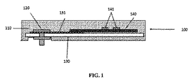
図1に例示されるように、テキスタイル基板130は、少なくとも1つの第2の電気的接続手段131を備え、少なくとも1つの第2の電気的接続手段131は、電子回路140に電気的に接続される。
As illustrated in FIG. 1, the
一実施形態において、少なくとも1つの第2の電気的接続手段は、導電ワイヤ、又は導電性インクもしくはペイントである。インク又は導電性ペイントは、電気伝導性材料が混ぜ込まれ、可撓な特性を有し、このインク又は導電性ペイントをフレキシブル表面に置くことが可能である。一実施形態において、テキスタイル基板は、複数の第2接続手段を備える。一実施形態において、少なくとも1つの第2の電気的接続手段は、相互接続トラックである。 In one embodiment, the at least one second electrical connection means is a conductive wire or a conductive ink or paint. The ink or conductive paint is mixed with an electrically conductive material and has flexible properties, and it is possible to place the ink or conductive paint on a flexible surface. In one embodiment, the textile substrate comprises a plurality of second connection means. In one embodiment, the at least one second electrical connection means is an interconnect track.
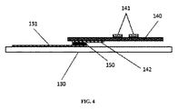
図2及び図3に例示される一実施形態において、少なくとも1つの第2の電気的接続手段131及び電子回路140は、溶接材150により電気的に接続される。好ましい実施形態において、溶接材は、はんだ付けペースト又ははんだペーストであり、当業者に知られ、習得された適切な融解処理により融解されるであろう。図4に例示される一実施形態において、はんだ材150は、テキスタイル基板130の少なくとも1つの第2の電気的接続手段131を電子回路の少なくとも1つの接続トラック142に電気的に接続する。
In one embodiment illustrated in FIGS. 2 and 3, the at least one second electrical connection means 131 and the
不図示の実施形態において、テキスタイル基板の少なくとも1つの第2の電気的接続手段及び電子回路の少なくとも1つの接続トラックは、機械的接続により接続される。一実施形態において、この機械的接続は、かしめによりなされる。この種の接続は、はんだ材150の使用及びはんだ材に関する全ての処理工程を回避することを可能にさせる。
In an embodiment not shown, at least one second electrical connection means of the textile substrate and at least one connection track of the electronic circuit are connected by a mechanical connection. In one embodiment, this mechanical connection is made by caulking. This type of connection makes it possible to avoid the use of the
テキスタイル基板の可撓性は、本発明に係るデバイスが、破損又は塑性変形なく、テキスタイルが変形を受けることを可能にする。一実施形態において、テキスタイル基板は、少なくとも部分的に弾性がある。一実施形態において、テキスタイル基板は、完全に弾性がある。弾性があるテキスタイル基板とは、塑性変形を受けることなく、その初期の長さの少なくとも10%、2方向への伸長を受けることができるテキスタイル基板を意味する。一実施形態において、テキスタイル基板は、塑性変形を受けることなく、その初期の長さの15、20、25、30、40、50、60、70、80、90、100、150、200、300、又は500パーセント、2方向に伸長することができる。織りという観点において、2方向とは、枠の方向と縦糸の方向を意味する。編みという観点において、2方向とは、編み段の方向と編み目の縦列の方向を意味する。 The flexibility of the textile substrate allows the device according to the invention to undergo a deformation of the textile without breakage or plastic deformation. In one embodiment, the textile substrate is at least partially elastic. In one embodiment, the textile substrate is completely elastic. An elastic textile substrate means a textile substrate that can be stretched in two directions at least 10% of its initial length without undergoing plastic deformation. In one embodiment, the textile substrate is subjected to its initial length of 15, 20, 25, 30, 40, 50, 60, 70, 80, 90, 100, 150, 200, 300, without undergoing plastic deformation. Or it can stretch 500 percent in two directions. From the viewpoint of weaving, the two directions mean the direction of the frame and the direction of the warp. From the viewpoint of knitting, the two directions mean the direction of the knitting steps and the direction of the columns of the stitches.
一実施形態において、テキスタイル基板は、フレキシブルテキスタイル糸を織ることにより作られる。一実施形態において、フレキシブルテキスタイル糸は、塑性変形を受けることなく、その初期の長さの少なくとも10%、縦方向への伸長を受けることができる。一実施形態において、フレキシブルテキスタイル糸は、塑性変形を受けることなく、その初期の長さの15、20、25、30、40、50、60、70、80、90、100、150、200%、300、又は500%、縦方向への伸長を受けることができる。 In one embodiment, the textile substrate is made by weaving flexible textile yarns. In one embodiment, the flexible textile yarn is capable of undergoing longitudinal elongation at least 10% of its initial length without undergoing plastic deformation. In one embodiment, the flexible textile yarn is subjected to 15, 20, 25, 30, 40, 50, 60, 70, 80, 90, 100, 150, 200% of its initial length without undergoing plastic deformation, 300 or 500% can be stretched in the machine direction.
別の実施形態において、テキスタイル基板は、フレキシブル糸を編むこと又はそれ以外の方法により作られる。編まれた構造は、基板に弾性の特性を与える。 In another embodiment, the textile substrate is made by knitting a flexible yarn or otherwise. The knitted structure gives the substrate elastic properties.
別の実施形態において、テキスタイル基板は、刺繍、レース、裁縫、又は当業者に既知な任意の他の手段により作られる。 In another embodiment, the textile substrate is made by embroidery, lace, sewing, or any other means known to those skilled in the art.
一実施形態において、電子回路とテキスタイル基板の間にある電気的接続域への機械的応力を制限するため、電子回路とテキスタイル基板の間の機械的結合力は、これら2つの部分間において接着剤箇所など他の手段により補強される。 In one embodiment, in order to limit the mechanical stress on the electrical connection area between the electronic circuit and the textile substrate, the mechanical coupling force between the electronic circuit and the textile substrate is between the two parts. Reinforced by other means such as a point.
本発明に係るデバイスは、テキスタイルの導電域に接続するようになされる少なくとも1つの第1の機械的及び電気的接続手段を備える。 The device according to the invention comprises at least one first mechanical and electrical connection means adapted to connect to the conductive area of the textile.
少なくとも1つの第1の機械的及び電気的接続手段は、少なくとも1つの第2の電気的接続手段とテキスタイルの導電域の間に電気的接続を提供する。 At least one first mechanical and electrical connection means provides an electrical connection between the at least one second electrical connection means and the conductive area of the textile.
一実施形態において、少なくとも1つの第1の機械的及び電気的接続手段は、テキスタイル基板の少なくとも1つの第2の電気的接続手段の端に配される。 In one embodiment, the at least one first mechanical and electrical connection means is arranged at the end of the at least one second electrical connection means of the textile substrate.
少なくとも1つの第1の機械的及び電気的接続手段は、本発明に係るデバイスとテキスタイルの導電域の間の機械的接続をも提供する。 The at least one first mechanical and electrical connection means also provides a mechanical connection between the device according to the invention and the conductive area of the textile.
図7に表される一実施形態において、テキスタイルの導電域210は、デバイスの機械的及び電気的接続の少なくとも1つの第1手段120を受けることを補う又はそれができる少なくとも1つの接続手段220を備える。一実施形態において、少なくとも1つの第1の機械的及び電気的接続手段120は、押しボタンである。代替実施形態において、少なくとも1つの第1の機械的及び電気的接続手段120は、テキスタイル基板130の少なくとも1つの第2の電気的接続手段の端で基板テキスタイルにかしめられる又は縫い付けられるスライダー(すなわち、ジッパー)と嵌合する歯を有するデバイスの構成要素である。別の代替実施形態において、少なくとも1つの第1の機械的及び電気的接続手段120は、例えば、電気伝導性磁石又は強磁性板など電気伝導性磁気接続手段である。別の実施形態において、少なくとも1つの第1の機械的及び電気的接続手段120は、リベットである。 In one embodiment represented in FIG. 7, the textile conductive area 210 comprises at least one connection means 220 that supplements or is capable of receiving at least one first means 120 of mechanical and electrical connection of the device. Prepare. In one embodiment, the at least one first mechanical and electrical connection means 120 is a push button. In an alternative embodiment, the at least one first mechanical and electrical connection means 120 is a slider (i.e., crimped or sewn to the substrate textile at the end of the at least one second electrical connection means of the textile substrate 130). , Zipper), a component of a device having teeth that mate with it. In another alternative embodiment, the at least one first mechanical and electrical connection means 120 is an electrically conductive magnetic connection means such as, for example, an electrically conductive magnet or a ferromagnetic plate. In another embodiment, the at least one first mechanical and electrical connection means 120 is a rivet.
フレキシブルエンベローブは、デバイス全体に電子回路及び電気部品のための保護構造を与えることが可能である。 Flexible envelopes can provide a protective structure for electronic circuits and electrical components throughout the device.
フレキシブルエンベローブは、(コーティングされている又はされていないテキスタイルの種類に応じて)部分的に又は完全にテキスタイル200によってもたらされることもできる。
The flexible envelope can also be provided by the
フレキシブルエンベローブは、電子回路、少なくとも1つの第1の機械的及び電気的接続手段、及びテキスタイル基板を完全に又は部分的に包囲する。少なくとも1つの第1の機械的及び電気的接続手段は、テキスタイルに接続することができるように、フレキシブルエンベローブを抜けて、少なくとも部分的に接触可能である。図1に例示される本発明の一実施形態において、少なくとも1つの第1の機械的及び電気的接続手段120は、フレキシブルエンベローブ110から突出し、フレキシブルエンベローブ110を抜けて、少なくとも部分的に接触可能である。不図示の代替実施形態において、フレキシブルエンベローブは、少なくとも1つの第1の機械的及び電気的接続手段が、フレキシブルエンベローブを抜けて、少なくとも部分的に接触可能となるように、少なくとも1つの第1の機械的及び電気的接続手段のある部位にオリフィス開口を保持する。
The flexible envelope completely or partially surrounds the electronic circuit, the at least one first mechanical and electrical connection means, and the textile substrate. At least one first mechanical and electrical connection means is at least partially accessible through the flexible envelope so that it can be connected to the textile. In one embodiment of the invention illustrated in FIG. 1, at least one first mechanical and electrical connection means 120 protrudes from the
フレキシブルエンベローブは、デバイスの可撓性の制御を提供し、その局所的な剛性により、電子回路の完全な状態を保護しつつ、テキスタイル又は衣料への設置を可能にする。電子部品が電子回路にはんだ付けされる実施形態において、フレキシブルエンベローブは、電子部品のはんだの完全な状態を保護する。フレキシブルエンベローブは、デバイスを曲げている間、例えば、ユーザーが手で触れ動かしている間、接触することができるようデバイスの内部信号の電気的絶縁を提供する。フレキシブルエンベローブは、液体及び汚染(埃、異物など)の防止部である。こうして、この封止は、特にテキスタイルの洗浄又はユーザーの蒸泄の間、デバイスの劣化を防ぐことを可能にさせる。 The flexible envelope provides control of the flexibility of the device, and its local stiffness allows it to be installed in a textile or garment while protecting the complete state of the electronic circuit. In embodiments where the electronic component is soldered to an electronic circuit, the flexible envelope protects the integrity of the electronic component solder. The flexible envelope provides electrical isolation of the device's internal signals so that it can be touched while the device is bent, for example, while the user touches and moves it. The flexible envelope is a liquid and contamination (dust, foreign matter, etc.) prevention unit. Thus, this sealing makes it possible to prevent degradation of the device, especially during textile cleaning or user digestion.
一実施形態において、フレキシブルエンベローブは、可撓性ポリマー製である。一実施形態において、フレキシブルエンベローブは、エラストマー製、ポリウレタン製、ゴム製、又はシリコーン製である。 In one embodiment, the flexible envelope is made of a flexible polymer. In one embodiment, the flexible envelope is made of elastomer, polyurethane, rubber, or silicone.
一実施形態において、フレキシブルエンベローブは、ワニスの層である。同一実施形態において、フレキシブルエンベローブは、少なくとも1つの有機溶媒、可塑剤、及び/又はプラスチック膜を形成することができる物質を含む組成物により形成される。乾燥により、この組成物は、ワニスの層(フレキシブルエンベローブ)を形成し、本発明に係るデバイスに対し、可撓性、液体及び汚染からの封止、保護、及び電気的絶縁を保証する。 In one embodiment, the flexible envelope is a layer of varnish. In the same embodiment, the flexible envelope is formed by a composition comprising at least one organic solvent, a plasticizer, and / or a material capable of forming a plastic film. Upon drying, the composition forms a layer of varnish (flexible envelope), ensuring flexibility, sealing from liquids and contamination, protection and electrical insulation for the device according to the invention.
一実施形態において、デバイスは、塑性変形を受けることなく、半径5〜10cmの円柱片上で曲がる可撓性を有する。この可撓性により、デバイスは、デバイスが埋め込まれることになっている衣服の動き及び変形に、損傷することなく合わせることが可能となる。 In one embodiment, the device has the flexibility to bend on a cylindrical piece with a radius of 5-10 cm without undergoing plastic deformation. This flexibility allows the device to adapt to the movement and deformation of the garment in which the device is to be implanted without damage.
一実施形態において、デバイスは、10mm未満、好ましくは5mm未満、さらに好ましくは3mm未満の厚さである。 In one embodiment, the device is less than 10 mm thick, preferably less than 5 mm, more preferably less than 3 mm.
本発明は、本発明に係るテキスタイルデバイスと、導電域、及びデバイスの機械的及び電気的接続の少なくとも1つの第1手段に取り外し可能な方途で接続することができる少なくとも1つの機械的及び電気的接続手段を備えるテキスタイルとを備えるシステムにも関する。この少なくとも1つのテキスタイル接続は、本発明に係るデバイスをテキスタイルの導電域に電気的及び機械的に接続することを可能にさせる。 The present invention comprises at least one mechanical and electrical connection that can be connected in a removable manner to a textile device according to the present invention and at least one first means of electrical conduction area and mechanical and electrical connection of the device. It also relates to a system comprising a textile comprising connecting means. This at least one textile connection makes it possible to electrically and mechanically connect the device according to the invention to the conductive area of the textile.
一実施形態において、テキスタイルの導電域は、導電糸を織る又は編むことにより作られる。 In one embodiment, the textile conductive area is created by weaving or knitting conductive yarns.
一実施形態において、これら導電ワイヤは、銀などの導電性材料からなる。 In one embodiment, the conductive wires are made of a conductive material such as silver.
代替実施形態において、これら導電糸は、導電性材料で覆われたテキスタイル糸、好ましくは導電性金属で覆われたテキスタイル糸、最も好ましくは銀で覆われたテキスタイル糸からなる。 In an alternative embodiment, these conductive yarns consist of textile yarns covered with a conductive material, preferably textile yarns covered with conductive metal, most preferably textile yarns covered with silver.
別の実施形態において、テキスタイルの導電領域は、導電性インク又は導電性ペイントにより得られる。この実施形態において、インク又は導電性ペイントは、インク又は導電性ペイントをフレキシブル表面に置くことを可能にする可撓な特性を有する電気伝導性材料が混ぜ込まれる。 In another embodiment, the textile conductive region is obtained by conductive ink or conductive paint. In this embodiment, the ink or conductive paint is mixed with an electrically conductive material having flexible properties that allow the ink or conductive paint to be placed on a flexible surface.
一実施形態において、テキスタイルの電気的及び機械的接続の少なくとも1つの手段は、テキスタイルの少なくとも1つの導電域に設けられる。一実施形態において、フレキシブル電子デバイスの少なくとも1つの第1の機械的及び電気的接続手段及び少なくとも1つのテキスタイル接続手段は、相補性がある。一実施形態において、フレキシブル電子デバイスの少なくとも1つの第1の機械的及び電気的接続手段及びテキスタイルを接続するための少なくとも1つの手段は、一方が他方に取り外し可能な様式ではめ込まれる。 In one embodiment, at least one means of electrical and mechanical connection of the textile is provided in at least one conductive area of the textile. In one embodiment, the at least one first mechanical and electrical connection means and the at least one textile connection means of the flexible electronic device are complementary. In one embodiment, at least one first mechanical and electrical connection means and at least one means for connecting the textile of the flexible electronic device are fitted in a removable manner, one to the other.
図7に例示される実施形態において、フレキシブル電子デバイスの少なくとも1つの第1の機械的及び電気的接続手段120は、雄型接続手段であり、テキスタイルの接続手段220は、雌型接続手段である。不図示の実施形態において、フレキシブル電子デバイスの少なくとも1つの第1の機械的及び電気的接続手段は、雌型接続手段であり、少なくとも1つのテキスタイル接続手段は、雄型接続手段である。不図示の実施形態において、フレキシブル電子デバイスの少なくとも1つの第1の機械的及び電気的接続手段は、整列した歯の列であり、少なくとも1つのテキスタイル接続手段は、整列した歯の第2の列であり、2つの列のうち一方は、歯を互いに嵌合するためのスライダー(すなわち、ジッパー)を備える。代替実施形態において、テキスタイル電子デバイスの少なくとも1つの第1の機械的及び電気的接続手段及び少なくとも1つのテキスタイル接続手段は、導電性磁気接続手段又は提示される全ての実施形態の組み合わせである。前述の実施形態において、少なくとも1つの第1の及び少なくとも1つの第2の機械的及び電気的接続手段は、使用が容易であり、そのため、ユーザーが医師又は技術者の介入なくテキスタイル電子デバイス100をテキスタイル導電域200に着脱することを可能にさせる。
In the embodiment illustrated in FIG. 7, the at least one first mechanical and electrical connection means 120 of the flexible electronic device is a male connection means and the textile connection means 220 is a female connection means. . In an embodiment not shown, at least one first mechanical and electrical connection means of the flexible electronic device is a female connection means and at least one textile connection means is a male connection means. In an embodiment not shown, the at least one first mechanical and electrical connection means of the flexible electronic device is an array of aligned teeth, and the at least one textile connection means is a second array of aligned teeth. And one of the two rows comprises a slider (i.e. a zipper) for fitting the teeth together. In an alternative embodiment, the at least one first mechanical and electrical connection means and the at least one textile connection means of the textile electronic device are conductive magnetic connection means or a combination of all the presented embodiments. In the foregoing embodiments, the at least one first and at least one second mechanical and electrical connection means are easy to use, so that the user can connect the textile
一実施形態において、使用されるテキスタイル200は、塑性変形又は破損を受けることなく、少なくとも15%伸長することができるテキスタイルである。一実施形態において、使用テキスタイル200は、塑性変形を受けることなく、少なくとも20、25、30、40、50、75、100、150、200%伸長することができる。本実施形態は、ユーザーの肌と接触して着用することができる衣服を提供する。ユーザーの肌とのこの接触は、例えば、生体電位データを、例えば、同一テキスタイル200に組み込まれる電極を使用して測定することを可能にさせる。
In one embodiment, the
そのため、本発明に係る該デバイスは、最初に提示した技術的課題を解決する。 Therefore, the device according to the present invention solves the technical problem presented first.
本発明は、本発明に係るテキスタイル電子デバイスを製造する方法であって、
少なくとも1つの第2の電気的接続手段をテキスタイル基板上に置く工程と、
電子回路の少なくとも1つのトラックが第2の電気的接続手段と電気的に接触するように電子回路をテキスタイル基板上に置く工程と、
テキスタイル基板上に、テキスタイルの導電域に接続するようになされる少なくとも1つの第1の機械的及び電気的接続手段を固定する工程であって、少なくとも1つの第1の機械的及び電気的接続手段は、少なくとも1つの第2の電気的接続手段と電気的に接触する工程と、
電子回路と、少なくとも1つの第1の機械的及び電気的接続手段と、テキスタイル基板とを完全に又は部分的に含むフレキシブルエンベローブによりオーバーモールドする工程であって、少なくとも1つの第1の機械的及び電気的接続手段は、フレキシブルエンベローブを抜けて、少なくとも部分的に接触可能である工程と、
を含む方法にも関する。
The present invention is a method of manufacturing a textile electronic device according to the present invention,
Placing at least one second electrical connection means on the textile substrate;
Placing the electronic circuit on the textile substrate such that at least one track of the electronic circuit is in electrical contact with the second electrical connection means;
Fixing at least one first mechanical and electrical connection means adapted to be connected to the conductive area of the textile on the textile substrate, comprising at least one first mechanical and electrical connection means In electrical contact with at least one second electrical connection means;
Overmolding with a flexible envelope comprising completely or partly an electronic circuit, at least one first mechanical and electrical connection means and a textile substrate, comprising at least one first mechanical and electrical The electrical connection means is at least partially accessible through the flexible envelope;
It also relates to a method comprising:
代替実施形態において、オーバーモールドする工程は、電子回路と、少なくとも1つの第1の機械的及び電気的接続手段と、基板テキスタイルとを完全に又は部分的に含むフレキシブルエンベローブを形成する少なくとも2つの表面を溶接する工程であって、少なくとも1つの第1の機械的及び電気的接続手段は、フレキシブルエンベローブを抜けて、少なくとも部分的に接触可能である工程に置き替えられる。 In an alternative embodiment, the overmolding step comprises at least two surfaces forming a flexible envelope that is wholly or partly comprised of an electronic circuit, at least one first mechanical and electrical connection means, and a substrate textile. Wherein the at least one first mechanical and electrical connection means is replaced by a step that is at least partially accessible through the flexible envelope.
製造工程は、図面を考慮すれば、より理解されるであろう。 The manufacturing process will be better understood in view of the drawings.
図1は、フレキシブルエンベローブ110と、テキスタイル基板130と、少なくとも1つの第1の機械的及び電気的接続手段120と、電子回路140とを備える本発明の実施形態に係るデバイスの図解を表す。テキスタイル基板は、電子回路140を少なくとも1つの第1の機械的及び電気的接続手段120に接続する少なくとも1つの第2の電気的接続手段131を備える。
FIG. 1 represents an illustration of a device according to an embodiment of the present invention comprising a
少なくとも1つの第2の電気的接続手段をテキスタイル基板に置く第1工程の間、少なくとも1つの第2の電気的接続手段は、テキスタイル基板に縫い付けられる導電ワイヤ、もしくは印刷される、スクリーン印刷される、又はテキスタイル基板に任意の他の方法で置かれる導電性インクである。 During the first step of placing at least one second electrical connection means on the textile substrate, the at least one second electrical connection means is a conductive wire sewn on the textile substrate, or printed, screen printed. Or conductive ink placed in any other manner on the textile substrate.
デバイスの製造のための第1実施形態において、はんだ材150は、その後、図2に例示されるように、少なくとも1つの第2の電気的接続手段131に置かれる。
In a first embodiment for the manufacture of the device, the
電子回路140は、その後、図3に例示されるように、はんだ材150が少なくとも1つの第2電気的接続手段131及び電子回路140と接触するように、テキスタイル基板130上に置かれる。
The
図4に例示される実施形態において、電子回路は、接続トラック142を備える。その後の電気的接続を保証するため、電子回路140は、はんだ材150が少なくとも1つの第2の電気的接続手段131及び電子回路の接続トラック142と接触するように、テキスタイル基板130上に置かれる。
In the embodiment illustrated in FIG. 4, the electronic circuit comprises a
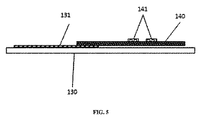
次の工程において、はんだ材150は、その融解温度を超える温度に加熱される。こうして融解した材料は、材料の連続性、及び少なくとも1つの第2の電気的接続手段131と電子回路140の間の大きな接触領域を作り出すことを可能にする。冷却されると、少なくとも1つの第2の電気的接続手段131は、電子回路140と電気的に接触する。この工程は、図5に示される。この図において、このときのはんだ材の厚さは電子回路又はテキスタイル基板に対してごく僅かであり、はんだ材は、もはや示されない。一実施形態において、溶接は、溶接材の局所的な加熱により実行される。代替実施形態において、はんだ材は、はんだペースト又ははんだペーストであり、加熱は、少なくとも、はんだ材により接続されるテキスタイル基板130及び電子回路140を、オーブンで、例えば、はんだペーストを再融解するよう設計されるリフロー炉で加熱することにより行われる。
In the next step, the
第2の代替実施形態において、電子回路140と第2の電気的接続手段131の間の接続は、機械的に、例えば、かしめにより行うことができ、溶接材150の使用を省くことを可能にさせる。
In a second alternative embodiment, the connection between the
少なくとも1つの第1の機械的及び電気的接続手段120は、図6に示されるように、フレキシブル基板130に固定される。この少なくとも1つの第1の機械的及び電気的接続手段120は、少なくとも1つの第2の電気的接続手段131に接続される。上述したように、少なくとも1つの第1の機械的及び電気的接続手段120は、テキスタイルの導電域に接続することができる。一実施形態において、図8に示されるように、少なくとも1つの第1の機械的及び電気的接続手段120は、テキスタイルに相似性又は相補性がある少なくとも1つの接続手段に接続するようになされる。
At least one first mechanical and electrical connection means 120 is secured to the
デバイスは、最終的に、フレキシブルエンベローブ110によりオーバーモールドされる。図7に表されるように、フレキシブルエンベローブは、電子回路140、少なくとも1つの第1の機械的及び電気的接続手段120、及びテキスタイル基板130を完全に又は部分的に包囲し、少なくとも1つの第1の機械的及び電気的接続手段120は、フレキシブルエンベローブ110を抜けて、少なくとも部分に接触可能である。一実施形態において、デバイスは、可撓性のあるオーバーモールド材が注入されるモールド内に配される。別の実施形態において、可撓性のあるオーバーモールド材は、吹き付け又は液体成膜によりデバイスに置かれる。
The device is finally overmolded with a
代替実施形態において、オーバーモールド工程は、電子回路140、少なくとも1つの第1の機械的及び電気的接続手段120、及びテキスタイル基板130を完全に又は部分的に含むフレキシブルエンベローブ110を形成する少なくとも2つの表面に溶接する工程であって、少なくとも1つの第1の機械的及び電気的接続手段120は、フレキシブルエンベローブ110を抜けて、部分的に接触可能である工程に置き替えられる。
In an alternative embodiment, the overmolding process forms at least two
一実施形態において、テキスタイル基板は、フレキシブルエンベローブの一部を、その表面の少なくとも一方に、前もって備える。 In one embodiment, the textile substrate previously comprises a portion of the flexible envelope on at least one of its surfaces.
本発明の一実施形態において、デバイスは、複数の第1の電気的及び機械的接続手段120を備える。一実施形態において、テキスタイル基板130は、各々、回路140、特に、接続トラック142、及び電気的及び機械的接続の第1手段に接続される複数の第2の電気的接続手段131を備える。一実施形態において、デバイスは、各々複数の電子回路140に複数の第2電気的接続手段131により接続される複数の第1の機械的及び電気的接続手段120を備える。
In one embodiment of the invention, the device comprises a plurality of first electrical and mechanical connection means 120. In one embodiment, the
様々な実施形態を述べ、例示したが、発明を実施するための形態は、本明細書の記載に限定されるものと解釈すべきではない。当業者であれば、特許請求の範囲により定義されるような本開示の真の精神及び範囲から逸脱することなく、様々な変形形態を実施形態とすることができる。 Although various embodiments have been described and illustrated, the forms for carrying out the invention should not be construed as limited to the description herein. Those skilled in the art can make various modifications to the embodiments without departing from the true spirit and scope of the present disclosure as defined by the claims.
100 テキスタイルの導電域に接続されるよう構成されるテキスタイル電子デバイス
110 フレキシブルエンベローブ
120 第1の機械的及び電気的接続手段
130 テキスタイル基板
131 第2の電気的接続手段
140 電子回路
141 電子部品
142 電子回路のトラック
150 溶接材
200 テキスタイル
210 テキスタイルの導電域
220 テキスタイルの機械的及び電気的接続の手段
DESCRIPTION OF
Claims (11)
電子回路(140)と、
前記テキスタイル(200)の前記導電域に接続されるように構成される少なくとも1つの第1の機械的及び電気的接続手段(120)と、
少なくとも1つの第2の電気的接続手段(131)を備えるテキスタイル基板(130)であって、前記少なくとも1つの第2の電気的接続手段は、前記電子回路(140)と前記少なくとも1つの第1の機械的及び電気的接続手段(120)とに電気的に接続する、テキスタイル基板(130)と、
前記電子回路(140)、前記少なくとも1つの第1の機械的及び電気的接続手段(120)、及び前記テキスタイル基板(130)を完全に又は部分的に含むフレキシブルエンベローブ(110)であって、前記少なくとも1つの第1の機械的及び電気的接続手段(120)は、前記フレキシブルエンベローブ(110)を抜けて、少なくとも部分的に接触可能であるフレキシブルエンベローブ(110)と、
を備える、テキスタイル電子デバイス(100)。 A textile electronic device (100) configured to be connected to a conductive area of a textile (200) comprising:
An electronic circuit (140);
At least one first mechanical and electrical connection means (120) configured to be connected to the conductive area of the textile (200);
A textile substrate (130) comprising at least one second electrical connection means (131), wherein the at least one second electrical connection means comprises the electronic circuit (140) and the at least one first electrical connection means. A textile substrate (130) electrically connected to the mechanical and electrical connection means (120) of
A flexible envelope (110) comprising the electronic circuit (140), the at least one first mechanical and electrical connection means (120), and the textile substrate (130) completely or partially; At least one first mechanical and electrical connection means (120) exits said flexible envelope (110) and is at least partially accessible, and a flexible envelope (110),
A textile electronic device (100) comprising:
少なくとも1つの第2の電気的接続手段(131)をテキスタイル基板(130)に置く工程と、
電子回路の少なくとも1つのトラックが前記第2の電気的接続手段(131)と電気的に接触するように前記電子回路(140)を前記テキスタイル基板(130)上に置く工程と、
前記テキスタイル基板(130)に、前記テキスタイルの前記導電域に接続するようになされる少なくとも1つの第1の機械的及び電気的接続手段(120)を固定する工程であって、前記少なくとも1つの第1の機械的及び電気的接続手段は、前記少なくとも1つの第2の電気的接続手段(131)と電気的に接触する工程と、
フレキシブルエンベローブ(110)をオーバーモールドする又は前記フレキシブルエンベローブ(110)を形成する2つの表面を溶接する工程であって、前記フレキシブルエンベローブ(110)は、前記電子回路(140)と、前記少なくとも1つの第1の機械的及び電気的接続手段(120)と、前記テキスタイル基板(130)とを完全に又は部分的に含み、前記少なくとも1つの第1の機械的及び電気的接続手段(120)は、前記フレキシブルエンベローブ(110)を抜けて、少なくとも部分的に接触可能である工程と、
を含む方法。 A method of manufacturing a textile electronic device (100) configured to be connected to at least one conductive area of a textile (200) comprising:
Placing at least one second electrical connection means (131) on the textile substrate (130);
Placing the electronic circuit (140) on the textile substrate (130) such that at least one track of the electronic circuit is in electrical contact with the second electrical connection means (131);
Securing at least one first mechanical and electrical connection means (120) adapted to connect to the conductive area of the textile to the textile substrate (130), the at least one first One mechanical and electrical connection means in electrical contact with said at least one second electrical connection means (131);
Overmolding a flexible envelope (110) or welding two surfaces forming said flexible envelope (110), said flexible envelope (110) comprising said electronic circuit (140) and said at least one Including at least one first mechanical and electrical connection means (120) and the textile substrate (130), the at least one first mechanical and electrical connection means (120) comprising: Exiting the flexible envelope (110) and being at least partially accessible;
Including methods.
はんだ材(150)を前記テキスタイル基板の前記少なくとも1つの第2の電気的接続手段(131)上に置くことと、
前記はんだ材(150)が、前記少なくとも1つの第2の電気的接続手段(131)及び前記電子回路(140)と接触するように前記電子回路(140)を前記テキスタイル基板(130)上に置くことと、
前記はんだ材の融解温度よりも高い温度に前記はんだ材(150)を加熱することと、
前記テキスタイル基板の前記少なくとも1つの第2の電気的接続手段(131)を前記電子回路(140)に電気的に接続させるために前記はんだ材(150)を冷却することと、
を含む、請求項9に記載の方法。 The steps of the manufacturing method of placing the electronic circuit (140) on the textile substrate (130) such that the at least one track of the electronic circuit is in electrical contact with the second electrical connecting means (131). ,
Placing solder material (150) on the at least one second electrical connection means (131) of the textile substrate;
The electronic circuit (140) is placed on the textile substrate (130) such that the solder material (150) contacts the at least one second electrical connection means (131) and the electronic circuit (140). And
Heating the solder material (150) to a temperature higher than the melting temperature of the solder material;
Cooling the solder material (150) to electrically connect the at least one second electrical connection means (131) of the textile substrate to the electronic circuit (140);
The method of claim 9, comprising:
Applications Claiming Priority (5)
| Application Number | Priority Date | Filing Date | Title |
|---|---|---|---|
| FR1660936 | 2016-11-10 | ||
| FR1660936A FR3058610B1 (en) | 2016-11-10 | 2016-11-10 | TEXTILE ELECTRONIC DEVICE FOR INTELLIGENT CLOTHES |
| TW106139076 | 2017-11-09 | ||
| TW106139076A TW201825012A (en) | 2016-11-10 | 2017-11-09 | Textile electronic device for smart clothing |
| PCT/FR2017/053072 WO2018087489A1 (en) | 2016-11-10 | 2017-11-10 | Textile electronic device for smart clothing |
Publications (2)
| Publication Number | Publication Date |
|---|---|
| JP2019536277A true JP2019536277A (en) | 2019-12-12 |
| JP2019536277A5 JP2019536277A5 (en) | 2020-11-12 |
Family
ID=57590693
Family Applications (1)
| Application Number | Title | Priority Date | Filing Date |
|---|---|---|---|
| JP2019524408A Pending JP2019536277A (en) | 2016-11-10 | 2017-11-10 | Textile electronic devices for smart clothing |
Country Status (7)
| Country | Link |
|---|---|
| US (1) | US10905006B2 (en) |
| EP (1) | EP3539363A1 (en) |
| JP (1) | JP2019536277A (en) |
| CN (1) | CN110115114A (en) |
| FR (1) | FR3058610B1 (en) |
| TW (1) | TW201825012A (en) |
| WO (1) | WO2018087489A1 (en) |
Families Citing this family (7)
| Publication number | Priority date | Publication date | Assignee | Title |
|---|---|---|---|---|
| CN113692783A (en) * | 2019-04-18 | 2021-11-23 | 松下知识产权经营株式会社 | Stretchable laminate, material for stretchable device, and stretchable device |
| FR3096865B1 (en) | 2019-06-03 | 2021-06-04 | Inst Mines Telecom | Electronic system to be mounted on a flexible support, especially textile |
| CA3165237A1 (en) * | 2019-12-18 | 2021-06-24 | Myant Inc. | Method of manufacturing textile with conductive yarns and integrated electronics |
| JP7457498B2 (en) * | 2019-12-25 | 2024-03-28 | ミャント インコーポレイテッド | electrical connectors |
| US20210307170A1 (en) * | 2020-03-30 | 2021-09-30 | Sanctuary Cognitive Systems Corporation | Sensory array for use with artificial skin and artificial skin with sensory array, useful in robotics |
| TWI732585B (en) * | 2020-06-05 | 2021-07-01 | 三芳化學工業股份有限公司 | Conductive film and manufacturing method thereof |
| US11589459B2 (en) | 2020-12-23 | 2023-02-21 | Nextiles, Inc. | Connectors for integrating conductive threads to non-compatible electromechanical devices |
Citations (1)
| Publication number | Priority date | Publication date | Assignee | Title |
|---|---|---|---|---|
| JP2004513247A (en) * | 2000-10-16 | 2004-04-30 | フォスター−ミラー・インク | Method for producing a textile product with electronic circuitry and an electrically active textile product |
Family Cites Families (11)
| Publication number | Priority date | Publication date | Assignee | Title |
|---|---|---|---|---|
| JPH03260177A (en) * | 1990-03-02 | 1991-11-20 | Toray Ind Inc | Fiber sheet-like article having excellent heat resistance and chemical resistance |
| GB9608847D0 (en) * | 1996-04-30 | 1996-07-03 | Pressac Ltd | Method of mounting circuit components on a flexible substrate |
| US7462035B2 (en) * | 2005-07-27 | 2008-12-09 | Physical Optics Corporation | Electrical connector configured as a fastening element |
| GB0606005D0 (en) * | 2006-03-27 | 2006-05-03 | Leftly Steven A | Security device for textile products |
| DE102009005706A1 (en) | 2009-01-22 | 2010-07-29 | Winker Massivumformung Gmbh & Co. Kg | Forming machine for manufacturing blank from wire like or rod like semi finished product, has camera, stop and motor connected with electronic control device such that blanks are separable from preset volume of product by separation device |
| DE202009005706U1 (en) * | 2009-04-16 | 2009-07-30 | Herrmann, Dieter, Dipl.-Ing. | Connection and contacting of electrically conductive textiles |
| US9338915B1 (en) * | 2013-12-09 | 2016-05-10 | Flextronics Ap, Llc | Method of attaching electronic module on fabrics by stitching plated through holes |
| CN105163491B (en) * | 2015-09-17 | 2018-03-06 | 北京代尔夫特电子科技有限公司 | A kind of method for packing of wearable electronic |
| EP3371855A1 (en) * | 2015-11-04 | 2018-09-12 | Google LLC | Connectors for connecting electronics embedded in garments to external devices |
| MX2018010877A (en) * | 2016-03-09 | 2019-03-28 | Peerbridge Health Inc | System and method for monitoring conditions of a subject based on wireless sensor data. |
| WO2017200949A1 (en) * | 2016-05-16 | 2017-11-23 | Google Llc | Interactive fabric |
-
2016
- 2016-11-10 FR FR1660936A patent/FR3058610B1/en active Active
-
2017
- 2017-11-09 TW TW106139076A patent/TW201825012A/en unknown
- 2017-11-10 JP JP2019524408A patent/JP2019536277A/en active Pending
- 2017-11-10 EP EP17808546.0A patent/EP3539363A1/en not_active Withdrawn
- 2017-11-10 US US16/348,595 patent/US10905006B2/en active Active
- 2017-11-10 WO PCT/FR2017/053072 patent/WO2018087489A1/en unknown
- 2017-11-10 CN CN201780077775.0A patent/CN110115114A/en active Pending
Patent Citations (1)
| Publication number | Priority date | Publication date | Assignee | Title |
|---|---|---|---|---|
| JP2004513247A (en) * | 2000-10-16 | 2004-04-30 | フォスター−ミラー・インク | Method for producing a textile product with electronic circuitry and an electrically active textile product |
Also Published As
| Publication number | Publication date |
|---|---|
| CN110115114A (en) | 2019-08-09 |
| US20190373724A1 (en) | 2019-12-05 |
| EP3539363A1 (en) | 2019-09-18 |
| FR3058610A1 (en) | 2018-05-11 |
| WO2018087489A1 (en) | 2018-05-17 |
| FR3058610B1 (en) | 2018-11-16 |
| US10905006B2 (en) | 2021-01-26 |
| TW201825012A (en) | 2018-07-16 |
Similar Documents
| Publication | Publication Date | Title |
|---|---|---|
| JP2019536277A (en) | Textile electronic devices for smart clothing | |
| US8146171B2 (en) | Digital garment using digital band and fabricating method thereof | |
| Stanley et al. | A review of connectors and joining technologies for electronic textiles | |
| CN108024721A (en) | For the flexible fabric ribbon bond with sensor and the clothes of electronic equipment | |
| EP2727521A1 (en) | Cloth electronization product and method | |
| US7753686B2 (en) | Velcro connector | |
| US10863780B2 (en) | Component for garment or textile product | |
| JP2021510000A (en) | Electronics-woven fabric interconnection methods and systems | |
| JP2019536277A5 (en) | ||
| US10548219B2 (en) | Stress relaxation substrate and textile type device | |
| JP6977289B2 (en) | Wearable smart device | |
| KR101635520B1 (en) | Interconnecting structures and thereof methods between conductive yarns and control board | |
| TWI703959B (en) | Stretchable wiring board and manufacturing method of stretchable wiring board | |
| CN106559955A (en) | For the stretchable flex circuit of wearable device | |
| US9705262B2 (en) | Electronic subassembly for apparel | |
| Mehmann et al. | Reversible contacting for smart textiles | |
| JP2018021270A (en) | Human body motion detecting wear | |
| JP7027695B2 (en) | Wearable smart device | |
| Bagci et al. | Flexible PCB connection methods for wearable energy harvesting applications | |
| KR101877115B1 (en) | Forming method of conductive fiber circuit | |
| JP2018090946A (en) | Electrical connections for wearables and other articles | |
| Toso | E-Textiles. Study of the interaction between devices, connection methods and substrates | |
| US10412830B2 (en) | System including a conductive textile and an electronic circuit unit and a method | |
| Komolafe | E-textile handling: Should I treat my e-textile as a normal garment | |
| JP7000697B2 (en) | Wearable smart device |
Legal Events
| Date | Code | Title | Description |
|---|---|---|---|
| A521 | Request for written amendment filed |
Free format text: JAPANESE INTERMEDIATE CODE: A523 Effective date: 20200930 |
|
| A621 | Written request for application examination |
Free format text: JAPANESE INTERMEDIATE CODE: A621 Effective date: 20200930 |
|
| A977 | Report on retrieval |
Free format text: JAPANESE INTERMEDIATE CODE: A971007 Effective date: 20211018 |
|
| A131 | Notification of reasons for refusal |
Free format text: JAPANESE INTERMEDIATE CODE: A131 Effective date: 20211109 |
|
| A02 | Decision of refusal |
Free format text: JAPANESE INTERMEDIATE CODE: A02 Effective date: 20220607 |