JP2019201032A - Manufacturing method for semiconductor device - Google Patents
Manufacturing method for semiconductor device Download PDFInfo
- Publication number
- JP2019201032A JP2019201032A JP2018092944A JP2018092944A JP2019201032A JP 2019201032 A JP2019201032 A JP 2019201032A JP 2018092944 A JP2018092944 A JP 2018092944A JP 2018092944 A JP2018092944 A JP 2018092944A JP 2019201032 A JP2019201032 A JP 2019201032A
- Authority
- JP
- Japan
- Prior art keywords
- semiconductor
- region
- manufacturing
- semiconductor device
- heat treatment
- Prior art date
- Legal status (The legal status is an assumption and is not a legal conclusion. Google has not performed a legal analysis and makes no representation as to the accuracy of the status listed.)
- Pending
Links
Images


Abstract
Description
本発明は、半導体装置の製造方法に関し、特に、炭化珪素を用いた半導体装置の製造方法に関する。 The present invention relates to a method for manufacturing a semiconductor device, and more particularly to a method for manufacturing a semiconductor device using silicon carbide.
炭化珪素(以下、SiCと記す)は、バンドギャップが広く、最大絶縁電界がシリコンと比較して約一桁大きいことから、SiCは、パワーデバイスの材料として注目されている。 Since silicon carbide (hereinafter referred to as SiC) has a wide band gap and a maximum insulating electric field that is about an order of magnitude larger than that of silicon, SiC has attracted attention as a material for power devices.
半導体に不純物を導入する方法として、拡散法およびイオン注入法が知られているが、SiCは、不純物拡散係数が小さいため、拡散法による不純物の導入が難しい。そのため、SiCでは、所定の不純物濃度や深さ分布を得るために、イオン注入法が用いられる。一般的に、イオン注入法により不純物を導入する場合、半導体基板内に格子間原子および格子欠陥が発生する。そのため、結晶性を回復させる目的、および、不純物を活性化させる目的で、熱処理を行う必要がある。 As a method for introducing impurities into a semiconductor, a diffusion method and an ion implantation method are known. However, since SiC has a small impurity diffusion coefficient, it is difficult to introduce impurities by the diffusion method. Therefore, in SiC, an ion implantation method is used to obtain a predetermined impurity concentration and depth distribution. In general, when impurities are introduced by an ion implantation method, interstitial atoms and lattice defects are generated in a semiconductor substrate. Therefore, it is necessary to perform heat treatment for the purpose of restoring crystallinity and activating impurities.
特許文献1および特許文献2には、イオン注入法によって、SiCからなる半導体層に不純物領域を形成し、その後、半導体層の表面を絶縁膜で覆った状態で、1400℃以上の温度で熱処理を行うことによって、不純物領域を活性化させる技術が開示されている。
In
特許文献3および特許文献4には、イオン注入法によって、SiCからなる半導体層に不純物領域を形成し、その後、減圧雰囲気で熱処理を行うことによって、半導体層の表面にカーボン層を形成する技術が開示されている。そして、カーボン層を形成する工程より高い圧力、且つ、高い温度の雰囲気中において更に熱処理を行うことで、不純物領域を活性化させる技術が開示されている。
特許文献5には、SiCからなる半導体層に不純物領域を形成し、その後、高速で熱処理を用いて、1000℃以上、且つ、1600℃以下の温度で第1熱処理を行う技術が開示されている。次に、第1熱処理よりも低い温度で第2の熱処理を施し、不純物領域を活性化させる技術が開示されている。また、ここでは、SiCの表面をカーボンなどの保護膜で覆っていない。 Patent Document 5 discloses a technique in which an impurity region is formed in a semiconductor layer made of SiC, and then a first heat treatment is performed at a temperature of 1000 ° C. or more and 1600 ° C. or less using heat treatment at high speed. . Next, a technique for activating the impurity region by performing a second heat treatment at a temperature lower than the first heat treatment is disclosed. Here, the surface of SiC is not covered with a protective film such as carbon.
特許文献6には、SiC基板に対して行う熱処理として、SiCの表面の元素が蒸発しない程度の照射パワーを有するレーザアニールが開示されており、KrFおよびXeClエキシマレーザが開示されている。
特許文献7には、SiC基板を加熱した状態において、SiCのバンドギャップエネルギー以上のエネルギーを有するレーザ光を照射する技術と、レーザのパワー密度を変化させて照射する方法とが開示されている。
特許文献8および特許文献9には、レーザアニールによるSiC基板の表面へのダメージを小さくするため、レーザアニールを補助するためのヒーターを用いた熱処理が開示されている。
SiCは、バンドギャップが大きいので、1500℃を超える高温の活性化アニールが必要とされている。しかしながら、このような高温アニールを長時間に亘って行うと、SiC基板の表面からの原子離脱が生じる問題、および、SiC基板の表面にマイグレーションが生じる問題によって、SiC基板の表面に凹凸が発生する。SiC基板の表面に凹凸が発生すると、この凹凸に電界が集中し、SiC基板に形成されるデバイスにおいて、リーク電流の増加の原因となる。すなわち、SiC基板の表面の凹凸によって、半導体装置の信頼性が低下する恐れがある。 Since SiC has a large band gap, activation annealing at a high temperature exceeding 1500 ° C. is required. However, when such high-temperature annealing is performed for a long time, unevenness is generated on the surface of the SiC substrate due to a problem that atoms are detached from the surface of the SiC substrate and a problem that migration occurs on the surface of the SiC substrate. . When irregularities occur on the surface of the SiC substrate, the electric field concentrates on the irregularities, which causes an increase in leakage current in a device formed on the SiC substrate. That is, the reliability of the semiconductor device may be reduced due to the unevenness of the surface of the SiC substrate.
また、SiC基板の表面の凹凸の発生を抑制するために、SiC基板の表面をカーボンなどの保護膜によって保護した後、SiC基板に対して高温アニールを実施する方法が用いられているが、上記の問題を解決するには、保護膜だけでは十分ではない。 Further, in order to suppress the occurrence of unevenness on the surface of the SiC substrate, a method of performing high-temperature annealing on the SiC substrate after the surface of the SiC substrate is protected by a protective film such as carbon is used. In order to solve this problem, a protective film alone is not sufficient.
一方で、レーザアニールを用いた活性化方法は、SiC基板に導入した不純物を活性化させる周波数を有する光に対して、SiC基板はその光の吸収係数が低いので、SiC基板の深い位置に形成された不純物領域を活性化するためには高エネルギーのレーザ照射が必要となる。しかしながら、高エネルギーのレーザ照射は、SiC基板の表面において、SiCの昇華が生じる問題がある。また、高エネルギーのレーザ照射に代えて、低エネルギーのレーザ照射を複数回に分けて実施する方法、および、レーザアニールの補助としてヒーター用いる方法は、ランニングコストの増加、アニール装置の改良、または、新規のアニール装置の導入など、多額の投資が必要となる問題がある。 On the other hand, the activation method using laser annealing is formed in a deep position of the SiC substrate because the light absorption coefficient of the SiC substrate is low with respect to light having a frequency for activating impurities introduced into the SiC substrate. In order to activate the impurity region, high energy laser irradiation is required. However, high-energy laser irradiation has a problem that SiC sublimation occurs on the surface of the SiC substrate. Further, instead of high-energy laser irradiation, a method of performing low-energy laser irradiation divided into a plurality of times, and a method of using a heater as an auxiliary to laser annealing, increase the running cost, improve the annealing apparatus, or There is a problem that requires a large amount of investment, such as the introduction of a new annealing device.
その他の課題と新規な特徴は、本明細書の記述および添付図面から明らかになるであろう。 Other problems and novel features will become apparent from the description of the specification and the accompanying drawings.
本願において開示される実施の形態のうち、代表的なものの概要を簡単に説明すれば、次のとおりである。 Of the embodiments disclosed in the present application, the outline of typical ones will be briefly described as follows.
一実施の形態である半導体装置の製造方法は、炭化珪素からなり、且つ、その表面上に半導体層が形成された半導体基板を準備する工程と、半導体層内に、第1半導体領域を形成する工程と、第1半導体領域に対して、レーザを用いた第1熱処理を行う工程と、を有する。また、半導体装置の製造方法は、更に、第1半導体領域上に保護膜を形成する工程と、第1半導体領域が保護膜で覆われた状態で、第1半導体領域、半導体層および半導体基板に対して、第2熱処理を行う工程、とを有する。 A method for manufacturing a semiconductor device according to an embodiment includes a step of preparing a semiconductor substrate made of silicon carbide and having a semiconductor layer formed on a surface thereof, and forming a first semiconductor region in the semiconductor layer. And a step of performing a first heat treatment using a laser on the first semiconductor region. The method for manufacturing a semiconductor device further includes a step of forming a protective film on the first semiconductor region, and the first semiconductor region, the semiconductor layer, and the semiconductor substrate in a state where the first semiconductor region is covered with the protective film. On the other hand, a step of performing a second heat treatment.
本願において開示される一実施の形態によれば、半導体装置の信頼性を向上させることができる。 According to one embodiment disclosed in the present application, the reliability of a semiconductor device can be improved.
以下、本発明の実施の形態を図面に基づいて詳細に説明する。なお、実施の形態を説明するための全図において、同一の機能を有する部材には同一の符号を付し、その繰り返しの説明は省略する。また、以下の実施の形態では、特に必要なときを除き、同一または同様な部分の説明を原則として繰り返さない。 Hereinafter, embodiments of the present invention will be described in detail with reference to the drawings. Note that components having the same function are denoted by the same reference symbols throughout the drawings for describing the embodiments, and the repetitive description thereof will be omitted. Also, in the following embodiments, the description of the same or similar parts will not be repeated in principle unless particularly necessary.
(実施の形態1)
<半導体装置の構造>
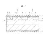
以下に、図1を用いて、本実施の形態の半導体装置の構造について説明する。図1は、半導体装置であるSiCパワーデバイスの一例として、2つのJBS(Junction Barrier Schottky)ダイオードDIの断面図を示している。なお、本実施の形態では、JBSダイオードDIの主要部のみを説明し、JBSダイオードDIの周辺部である電界緩和領域などについては、説明を省略する。
(Embodiment 1)
<Structure of semiconductor device>
Hereinafter, the structure of the semiconductor device of the present embodiment will be described with reference to FIG. FIG. 1 shows a cross-sectional view of two JBS (Junction Barrier Schottky) diodes DI as an example of a SiC power device which is a semiconductor device. In the present embodiment, only the main part of the JBS diode DI will be described, and description of the electric field relaxation region that is the peripheral part of the JBS diode DI will be omitted.
本実施の形態で使用される半導体基板1は、炭素および珪素を含む基板であり、具体的には、n型の不純物が導入された炭化珪素(SiC)基板である。半導体基板1の表面上には、相対的に低い不純物濃度を有するn型の半導体層2が形成されている。半導体層2も半導体基板1と同様に、炭素および珪素を含む。
The
半導体層2内には、半導体層2よりも高い不純物濃度を有するn型の半導体領域4が形成されている。半導体領域4内には、互いに分離されるように、複数のp型の半導体領域3が形成されている。n型の半導体領域4は、例えば2×10¹⁸/cm3の不純物濃度を有し、p型の半導体領域3は、例えば1×1018/cm3〜1×1020/cm3の不純物濃度を有する。
In the
半導体領域3上および半導体領域4上には、半導体領域3および半導体領域4に直接接するように、電極5が形成されている。電極5は、例えば、チタン膜と、チタン膜上に形成されたアルミニウム膜との積層の金属膜であり、半導体領域3および半導体領域4とショットキー接続されている。
An electrode 5 is formed on the
半導体基板1の裏面には、電極6が形成されている。電極6は、例えば、ニッケルシリサイドからなるシリサイド膜であり、半導体基板1とオーミック接続されている。
An
本実施の形態のJBSダイオードDIは、ショットキーバリアダイオードの一種であり、電極5と電極6との間の電流経路は、主に、n型の半導体領域4となる。そして、本実施の形態のJBSダイオードDIでは、n型の半導体領域4内に、複数のp型の半導体領域3が形成されている。JBSダイオードDIに逆方向のバイアスを印加した際に、電極5と半導体領域4との界面から半導体基板1へ向かって、リーク電流が流れる場合がある。この時、複数の半導体領域3から生じる空乏層によって、上記リーク電流の経路を狭めることで、上記リーク電流を抑制することができる。
The JBS diode DI of the present embodiment is a kind of Schottky barrier diode, and the current path between the electrode 5 and the
しかしながら、上述のように、半導体層2、半導体領域3および半導体領域4などに含まれる不純物を活性化させるため、長時間に亘って1500℃以上の高温の熱処理を行うと、半導体領域3および半導体領域4の表面に凹凸が発生し、凹凸に電界が集中するため、凹凸が上記リーク電流の増加の原因となる。従って、本実施の形態の半導体装置であるJBSダイオードDIの信頼性が低下する恐れがある。
However, as described above, when heat treatment at a high temperature of 1500 ° C. or higher is performed for a long time in order to activate impurities contained in the
このような恐れを解消するため、本実施の形態では、図1に示されるように、半導体領域3および半導体領域4の表面付近に活性化領域9が設けられている。活性化領域9は、例えば半導体領域3および半導体領域4の表面から100nmまでの深さに位置する領域であり、後述のレーザを用いた第1熱処理によって、結晶化された領域であり、半導体領域3および半導体領域4に含まれる不純物が活性化された領域である。
In order to eliminate such fear, in this embodiment, as shown in FIG. 1, an
以下に、本実施の形態の半導体装置の製造方法を説明しながら、活性化領域9の特徴を詳細に説明する。
Hereinafter, the characteristics of the
<半導体装置の製造方法>
図2〜図4は、図1に示される半導体装置の製造方法を示す断面図である。
<Method for Manufacturing Semiconductor Device>
2 to 4 are cross-sectional views showing a method of manufacturing the semiconductor device shown in FIG.
図2に示されるように、まず、その表面にn型の半導体層2が形成された半導体基板1を準備する。半導体基板1は、炭素および珪素を含む基板であり、n型の不純物が導入された炭化珪素(SiC)基板である。半導体層2は、エピタキシャル成長法によって半導体基板1上に形成され、炭素および珪素を含む層である。
As shown in FIG. 2, first, a
次に、イオン注入法によって、半導体層2内に、半導体層2よりも高い不純物濃度を有するn型の半導体領域4を形成する。半導体領域4は、例えば窒素をイオン注入することで形成され、窒素のドーズ量は、例えば1.6×10¹²/cm2である。ここでは、半導体領域4は、半導体層2の表面から800nm〜850nmの深さにかけて形成される。なお、このイオン注入は、1回だけでなく、注入エネルギーを変更して、複数回に分けて行われてもよい。
Next, an n-
図3は、半導体領域3の形成工程を示している。
FIG. 3 shows a process for forming the
まず、半導体領域4上に、例えば酸化シリコンからなる絶縁膜を形成する。次に、フォトリソグラフィ法およびエッチング処理を用いて、この絶縁膜をパターニングすることで、マスクパターン7を形成する。次に、半導体領域4の一部がマスクパターン7によって選択的に覆われた状態で、イオン8を半導体領域4に導入する。
First, an insulating film made of, for example, silicon oxide is formed on the
図3では、イオン8を矢印で示しており、イオン8には、イオン化したアルミニウムまたはホウ素が用いられる。また、イオン8のドーズ量は、例えば1.8×10¹⁴/cm2である。これにより、マスクパターン7から露出している半導体領域4内に、複数のp型の半導体領域3が形成される。ここでは、半導体領域3は、半導体層2の表面から600nm〜800nmの深さにかけて形成される。なお、このイオン注入は、1回だけでなく、注入エネルギーを変更して、複数回に分けて行われてもよい。
In FIG. 3, the
また、マスクパターン7の平面形状は、ストライプ状、島状、多角形状または格子状とすることが可能である。その後、ウェットエッチング処理などによって、マスクパターン7が除去される。
The planar shape of the
図4は、レーザを用いた第1熱処理工程、および、拡散炉を用いた高温の第2熱処理工程を示している。 FIG. 4 shows a first heat treatment step using a laser and a high temperature second heat treatment step using a diffusion furnace.
まず、半導体領域3および半導体領域4の表面付近に対して、レーザを用いた第1熱処理を行う。ここでは、SiCのバンドギャップエネルギー以上のエネルギーを有し、且つ、波長が248nmであるKrFエキシマレーザを用いる。これにより、半導体領域3および半導体領域4の表面付近の不純物を活性化させ、活性化領域9が形成される。具体的には、活性化領域9は、半導体領域3および半導体領域4の表面から100nmまでの深さにかけて、半導体領域3および半導体領域4に含まれる不純物が活性化された領域である。また、このレーザを用いた第1熱処理によって、活性化領域9の結晶性も良好となる。
First, a first heat treatment using a laser is performed on the vicinity of the surfaces of the
次に、半導体領域3上および半導体領域4上に、例えばカーボン膜または有機膜である保護膜10を形成する。次に、半導体領域3および半導体領域4が保護膜10によって覆われた状態で、半導体領域4、半導体領域3、半導体層2および半導体基板1に対して、拡散炉を用いた第2熱処理を行う。この第2熱処理は、1500℃以上の温度で行われ、例えば1500℃〜2000℃の範囲の温度で行われる。また、保護膜10は、主に、第2熱処理によって、半導体基板1の表面からの原子離脱が生じる問題、および、半導体基板1の表面にマイグレーションが生じる問題を出来るだけ抑制するために設けられている。このような第2熱処理により、半導体領域4、半導体領域3、半導体層2および半導体基板1に含まれる不純物が活性化される。その後、ウェットエッチング処理などによって、保護膜10が除去される。
Next, a
また、本実施の形態では、レーザを用いた第1熱処理を行った後に、保護膜10を形成した例を示したが、先に保護膜10を形成し、半導体領域3および半導体領域4が保護膜10によって覆われた状態で、レーザを用いた第1熱処理を行い、続けて拡散炉を用いた第2熱処理を行ってもよい。しかし、この場合、保護膜10がカーボン膜であると、KrFエキシマレーザが保護膜10に吸収されてしまう恐れがあるので、保護膜10には、レーザ波長の吸収率が低い膜として、有機膜を用いることが好ましい。
In the present embodiment, the
その後、以下の製造工程を経て、図1に示される半導体装置であるJBSダイオードDIが製造される。 Thereafter, the JBS diode DI which is the semiconductor device shown in FIG. 1 is manufactured through the following manufacturing process.
まず、半導体領域3上および半導体領域4上に、例えばスパッタリング法を用いて、例えばチタン膜と、アルミニウム膜とを順次形成する。次に、図示はしないが、フォトリソグラフィ法およびエッチング処理を用いて、チタン膜と、アルミニウム膜との積層の金属膜をパターニングすることで、電極5が形成される。電極5は、半導体領域3および半導体領域4に直接接するように形成され、半導体領域3および半導体領域4とショットキー接続される。
First, for example, a titanium film and an aluminum film are sequentially formed on the
次に、半導体基板1の裏面上に、例えばスパッタリング法を用いて、例えばニッケルからなる金属膜を形成する。次に、この金属膜に対して熱処理を行うことで、半導体基板1に含まれる材料と、上記金属膜に含まれる材料とを反応させて、ニッケルシリサイドからなるシリサイド膜を形成する。このシリサイド膜が半導体基板1とオーミック接続され、電極6となる。
Next, a metal film made of, for example, nickel is formed on the back surface of the
<本実施の形態の主な特徴>
本実施の形態の主な特徴は、図4で説明したように、まず、半導体領域3および半導体領域4の表面付近に対して、レーザを用いた第1熱処理を行い、その後、半導体領域4、半導体領域3、半導体層2および半導体基板1に対して、拡散炉を用いた1500℃以上の第2熱処理を行うことである。
<Main features of this embodiment>
As described in FIG. 4, the main feature of the present embodiment is that first, heat treatment using a laser is performed on the
上述のように、1500℃以上の高温の熱処理によって、各領域の不純物を活性化しようとすると、半導体領域3および半導体領域4の表面に凹凸が発生する。一方で、レーザを用いた熱処理は、SiCのレーザ吸収係数が低いので、深い位置に形成された不純物領域を活性化するためには高エネルギーのレーザ照射が必要となる。しかしながら、高エネルギーのレーザ照射は、SiCの昇華が生じる問題がある。
As described above, when the impurity in each region is activated by heat treatment at a high temperature of 1500 ° C. or higher, irregularities are generated on the surfaces of the
本実施の形態では、まず、半導体領域3および半導体領域4の表面付近に対して、レーザを用いた第1熱処理を行い、活性化領域9を形成している。活性化領域9において、半導体領域3および半導体領域4に含まれる不純物は活性化され、半導体領域3および半導体領域4の表面の結晶性も改善されている。活性化領域9の結晶性が良好であれば、後の1500℃以上の高温の第2熱処理による元素離脱が生じ難いため、半導体領域3および半導体領域4の表面に凹凸が発生し難くなる。
In the present embodiment, first, an
特に、本実施の形態のようなJBSダイオードDIでは、ショットキー接続がされている半導体領域3の表面の状態が良好であることが重要である。半導体領域3の表面が凹凸であると、凹凸に電界が集中するため、凹凸がリーク電流の増加の原因となる問題があり、更に、凹凸によって半導体領域3と電極5との接触面積が低減する問題があるからである。
In particular, in the JBS diode DI as in the present embodiment, it is important that the surface state of the
このように、リーク電流の増加を抑制するためには、半導体領域3の表面の凹凸を選択的に改善することが効率的である。そこで、本実施の形態では、レーザを用いた第1熱処理を行い、比較的深さの浅い活性化領域9のみを効率的に結晶化している。具体的には、半導体領域3および半導体領域4の表面から100nmまでの深さの領域が、活性化領域9として形成されている。このため、高エネルギーのレーザ照射を用いて、半導体基板1上の各領域(半導体層2、半導体領域3および半導体領域4)の全体を結晶化および活性化させる必要が無いので、SiCの昇華が生じるような問題を抑制できる。
As described above, in order to suppress an increase in leakage current, it is efficient to selectively improve the unevenness of the surface of the
また、第1熱処理に続いて、1500℃以上の高温の第2熱処理が行われるが、この時には既に、半導体領域3および半導体領域4の表面(活性化領域9)において、結晶性が改善されているため、半導体領域3および半導体領域4の表面は、凹凸が形成され難い状態となっている。すなわち、先にレーザを用いた第1熱処理が行われていることで、次に高温の第2熱処理を行っても、半導体領域3および半導体領域4の表面には、凹凸が発生し難い。このため、本実施の形態では、半導体装置の信頼性を向上させることができる。
Further, following the first heat treatment, a second heat treatment at a high temperature of 1500 ° C. or higher is performed. At this time, the crystallinity has already been improved on the surfaces of the
(実施の形態2)
以下に、実施の形態2の半導体装置を、図5を用いて説明する。図5は、実施の形態1の図4に対応する製造工程の断面図を示している。なお、以下の説明では、実施の形態1との相違点を主に説明する。
(Embodiment 2)
Hereinafter, the semiconductor device of the second embodiment will be described with reference to FIG. FIG. 5 shows a cross-sectional view of the manufacturing process corresponding to FIG. 4 of the first embodiment. In the following description, differences from the first embodiment will be mainly described.
実施の形態1では、図4に示されるように、p型の半導体領域3およびn型の半導体領域4に対して、レーザを用いた第1熱処理を行っていた。
In the first embodiment, as shown in FIG. 4, the first heat treatment using a laser is performed on the p-
実施の形態2では、図5に示されるように、n型の半導体領域4に対して、レーザを用いた第1熱処理を行うが、p型の半導体領域3に対して、レーザを用いた第1熱処理を行わない。すなわち、半導体領域3の表面に活性化領域19を形成するが、半導体領域4の表面に活性化領域19を形成しない。
In the second embodiment, as shown in FIG. 5, the n-
上述のように、JBSダイオードDIの電流経路は、主に、n型の半導体領域4である。このため、n型の半導体領域4の表面における凹凸の発生が抑制されることは、p型の半導体領域3の表面における凹凸の発生が抑制されることよりも重要である。
As described above, the current path of the JBS diode DI is mainly the n-
従って、実施の形態2では、半導体領域4に対して、レーザを用いた第1熱処理を選択的に行っている。レーザ照射は、半導体基板1の上方を自由に走査できるため、半導体領域4のみに選択的にレーザを照射させることができる。このように、実施の形態2では、実施の形態1と比較して、レーザを走査させる面積を低減させることができるので、製造時間の短縮を図ることができる。
Therefore, in the second embodiment, the first heat treatment using a laser is selectively performed on the
(変形例1)
以下に、変形例1の半導体装置を、図6を用いて説明する。図6は、実施の形態1の図4、および、実施の形態2の図5に対応する製造工程の断面図を示している。なお、以下の説明では、実施の形態1および実施の形態2との相違点を主に説明する。
(Modification 1)
Hereinafter, the semiconductor device of
変形例1では、まず、p型の半導体領域3およびn型の半導体領域4に対して、実施の形態1と同様に、レーザを用いた第1熱処理を行って、半導体領域3および半導体領域4の表面に活性化領域9を形成する。次に、n型の半導体領域4に対して、実施の形態2と同様に、レーザを用いた第3熱処理を選択的に行って、半導体領域4の表面に選択的に活性化領域19を形成する。なお、ここで説明する第3熱処理は、便宜上、名称を変更しているが、実施の形態2の第1熱処理と同じ処理である。
In the first modification, first, the first heat treatment using a laser is performed on the p-
また、変形例1では、上記第3熱処理を先に行い、その後、上記第1熱処理を行ってもよい。すなわち、変形例1では、半導体領域4に対してレーザを用いた熱処理が2回行われ、半導体領域3に対してレーザを用いた熱処理が1回行われる。
In
このように、変形例1では、半導体領域3および半導体領域4の表面において、結晶性を改善させると共に、半導体領域4の表面の結晶性を更に改善させることができる。従って、変形例1では、実施の形態1および実施の形態2と比較して、半導体装置の信頼性を更に向上させることができる。
Thus, in the first modification, the crystallinity can be improved on the surfaces of the
また、変形例1では、半導体領域4に対してレーザを用いた熱処理を2回行う場合を例示したが、必要に応じて、半導体領域4に対してレーザを用いた熱処理を3回以上行ってもよい。
In the first modification, the
(実施の形態3)
以下に、実施の形態3の半導体装置を、図7を用いて説明する。図7は、実施の形態1の図4に対応する製造工程の平面図を示しており、半導体基板1であるウェハWFの全体図を示している。また、図7は平面図であるが、図面を見易くするため、活性化領域29にハッチングを付している。なお、以下の説明では、実施の形態1との相違点を主に説明する。
(Embodiment 3)
The semiconductor device according to the third embodiment will be described below with reference to FIG. FIG. 7 is a plan view of the manufacturing process corresponding to FIG. 4 of the first embodiment, and shows an overall view of the wafer WF that is the
図7に示されるように、半導体基板1であるウェハWFは、ウェハWFの外周からウェハWFの中心に向かって幅W1を有する外周領域WPRと、平面視において外周領域WPRに囲まれた中央領域CRとを有する。なお、外周領域WPRには、オリエンテーションフラットが形成されている領域も含まれる。
As shown in FIG. 7, a wafer WF that is a
実施の形態3では、外周領域WPRに対して、実施の形態1と同様に、レーザを用いた第1熱処理を選択的に行い、中央領域CRに対しては、この第1熱処理を行わない。すなわち、外周領域WPRには、実施の形態1の活性化領域9と同様な活性化領域29が形成されている。
In the third embodiment, the first heat treatment using a laser is selectively performed on the outer peripheral region WPR as in the first embodiment, and the first heat treatment is not performed on the central region CR. That is, an
ウェハWFは、外周領域WPR、または、外周領域WPRおよび中央領域CRに亘って形成される半導体チップ領域CHP1と、中央領域CRに形成される半導体チップ領域CHP2とを有する。 Wafer WF has an outer peripheral region WPR, or a semiconductor chip region CHP1 formed over outer peripheral region WPR and central region CR, and a semiconductor chip region CHP2 formed in central region CR.
拡散炉を用いた1500℃以上の第2熱処理では、ウェハWF面内において、ばらつきが生じる。すなわち、中央領域CRよりも、外周領域WPRにおいて、半導体領域3および半導体領域4の表面に凹凸が生じ易いことが、本願発明者の検討により判った。言い換えれば、半導体チップ領域CH1に形成されるJBSダイオードDIは、半導体チップ領域CH2に形成されるJBSダイオードDIよりも、リーク電流が増加し易い傾向があり、同じウェハWFから製造されるJBSダイオードDIの性能にばらつきが生じる。
In the second heat treatment at 1500 ° C. or higher using the diffusion furnace, variation occurs in the wafer WF plane. That is, the inventors of the present application have found that the surface of the
そこで、実施の形態3では、外周領域WPRに対して、レーザを用いた第1熱処理を選択的に行うことで、外周領域WPRを含む半導体チップ領域CHP1において、半導体領域3および半導体領域4の表面の凹凸を抑制し、同じウェハWFから製造されるJBSダイオードDIの性能のばらつきを低減させている。すなわち、外周領域WPRにおけるJBSダイオードDIの性能の低下を抑制させている。このため、実施の形態3では、外周領域WPRにおける半導体装置の信頼性を向上させることができ、歩留まりを向上させることができる。
Therefore, in the third embodiment, the surface of the
(変形例2)
以下に、変形例2の半導体装置を、図8を用いて説明する。図8は、実施の形態1の図4、および、実施の形態3の図7に対応する製造工程の平面図を示しており、半導体基板1であるウェハWFの全体図を示している。また、図8は平面図であるが、図面を見易くするため、活性化領域29にハッチングを付している。なお、以下の説明では、実施の形態1および実施の形態3との相違点を主に説明する。
(Modification 2)
Hereinafter, a semiconductor device of
変形例2では、まず、外周領域WPRおよび中央領域CRに対して、実施の形態1と同様に、レーザを用いた第1熱処理を行って、活性化領域9を形成する。次に、外周領域WPRに対して、実施の形態3と同様に、レーザを用いた第4熱処理を選択的に行って、活性化領域29を形成する。なお、ここで説明する第4熱処理は、便宜上、名称を変更しているが、実施の形態3の第1熱処理と同じ処理である。
In the second modification, first, the
また、変形例2では、上記第4熱処理を先に行い、その後、上記第1熱処理を行ってもよい。すなわち、変形例2では、外周領域WPRに対してレーザを用いた熱処理が2回行われ、中央領域CRに対してレーザを用いた熱処理が1回行われる。
In
このように、変形例2では、外周領域WPRおよび中央領域CRにおいて、半導体領域3および半導体領域4の表面の結晶性を改善させると共に、外周領域WPRにおいて、半導体領域3および半導体領域4の表面の結晶性を更に改善させることができる。従って、変形例2では、実施の形態1および実施の形態3と比較して、半導体装置の信頼性を更に向上させることができる。
As described above, in the second modification, the crystallinity of the surface of the
また、変形例2では、外周領域WPRに対してレーザを用いた熱処理を2回行う場合を例示したが、必要に応じて、外周領域WPRに対してレーザを用いた熱処理を3回以上行ってもよい。 In the second modification, the case where the heat treatment using the laser is performed twice on the outer peripheral region WPR is illustrated, but the heat treatment using the laser is performed three times or more on the outer peripheral region WPR as necessary. Also good.
以上、本願発明者によってなされた発明を実施の形態に基づき具体的に説明したが、本発明は前記実施の形態に限定されるものではなく、その要旨を逸脱しない範囲で種々変更可能である。 As mentioned above, although the invention made by the inventor of the present application has been specifically described based on the embodiments, the present invention is not limited to the above-described embodiments, and various modifications can be made without departing from the scope of the invention.
例えば、上述の実施の形態では、半導体基板1がn型のSiC基板である場合を例示したが、導電型を逆にしてもよい。すなわち、半導体基板1、半導体層2および半導体領域4をp型とし、半導体領域3をn型としてもよい。
For example, in the above-described embodiment, the case where the
1 半導体基板
2 半導体層
3 半導体領域
4 半導体領域
5 電極
6 電極
7 マスクパターン
8 イオン
9 活性化領域
10 保護膜
19 活性化領域
29 活性化領域
CHP1、CHP2 半導体チップ領域
CR 中央領域
W1 幅
WF ウェハ
WPR 外周領域
DESCRIPTION OF
Claims (14)
(b)前記半導体層内に、前記半導体層の不純物濃度よりも高い不純物濃度を有する前記第1導電型の第1半導体領域を形成する工程、
(c)前記(b)工程後、前記第1半導体領域に対して、レーザを用いた第1熱処理を行う工程、
(d)前記(b)工程後、前記第1半導体領域上に保護膜を形成する工程、
(e)前記(c)工程後および前記(d)工程後、前記第1半導体領域が前記保護膜で覆われた状態で、前記第1半導体領域、前記半導体層および前記半導体基板に対して、第2熱処理を行う工程、
を有する、半導体装置の製造方法。 (A) preparing a first conductivity type semiconductor substrate made of silicon carbide and having a first conductivity type semiconductor layer formed on the surface thereof;
(B) forming a first semiconductor region of the first conductivity type having an impurity concentration higher than the impurity concentration of the semiconductor layer in the semiconductor layer;
(C) a step of performing a first heat treatment using a laser on the first semiconductor region after the step (b);
(D) after the step (b), a step of forming a protective film on the first semiconductor region;
(E) After the step (c) and after the step (d), with the first semiconductor region covered with the protective film, the first semiconductor region, the semiconductor layer, and the semiconductor substrate, Performing a second heat treatment;
A method for manufacturing a semiconductor device, comprising:
前記(b)工程と前記(c)工程との間に、前記第1半導体領域内に、前記第1導電型と反対の第2導電型の第2半導体領域を形成する工程を更に有する、半導体装置の製造方法。 In the manufacturing method of the semiconductor device according to claim 1,
A semiconductor further comprising a step of forming a second semiconductor region of a second conductivity type opposite to the first conductivity type in the first semiconductor region between the step (b) and the step (c). Device manufacturing method.
前記(c)工程の前記第1熱処理は、前記第1半導体領域に対して行われ、前記第2半導体領域に対して行われない、半導体装置の製造方法。 In the manufacturing method of the semiconductor device according to claim 2,
The method for manufacturing a semiconductor device, wherein the first heat treatment in the step (c) is performed on the first semiconductor region and is not performed on the second semiconductor region.
前記(c)工程の前記第1熱処理は、前記第1半導体領域および前記第2半導体領域に対して行われる、半導体装置の製造方法。 In the manufacturing method of the semiconductor device according to claim 2,
The method for manufacturing a semiconductor device, wherein the first heat treatment in the step (c) is performed on the first semiconductor region and the second semiconductor region.
前記(b)工程と前記(e)工程との間に、前記第1半導体領域に対して、レーザを用いた第3熱処理を選択的に行う工程を更に有し、
前記第3熱処理は、前記第2半導体領域に対して行われない、半導体装置の製造方法。 In the manufacturing method of the semiconductor device according to claim 4,
A step of selectively performing a third heat treatment using a laser on the first semiconductor region between the step (b) and the step (e);
The method of manufacturing a semiconductor device, wherein the third heat treatment is not performed on the second semiconductor region.
前記(e)工程後、前記第1半導体領域および前記第2半導体領域に直接接するように、第1電極を形成する工程と、前記半導体基板の裏面に、第2電極を形成する工程とを更に有する、半導体装置の製造方法。 In the manufacturing method of the semiconductor device according to claim 2,
After the step (e), a step of forming a first electrode so as to be in direct contact with the first semiconductor region and the second semiconductor region, and a step of forming a second electrode on the back surface of the semiconductor substrate A method for manufacturing a semiconductor device.
前記半導体基板は、前記半導体基板の外周から前記半導体基板の中心へ向かって第1幅を有する第1領域と、平面視において、前記第1領域に囲まれた第2領域とを有し、
前記(c)工程の前記第1熱処理は、前記第1領域に対して行われ、前記第2領域に対して行われない、半導体装置の製造方法。 In the manufacturing method of the semiconductor device according to claim 1,
The semiconductor substrate has a first region having a first width from the outer periphery of the semiconductor substrate toward the center of the semiconductor substrate, and a second region surrounded by the first region in plan view,
The method of manufacturing a semiconductor device, wherein the first heat treatment in the step (c) is performed on the first region and is not performed on the second region.
前記半導体基板は、前記半導体基板の外周から前記半導体基板の中心へ向かって第1幅を有する第1領域と、平面視において、前記第1領域に囲まれた第2領域とを有し、
前記(b)工程と前記(e)工程との間に、前記第1領域に対して、レーザを用いた第4熱処理を選択的に行う工程を更に有し、
前記第4熱処理は、前記第2領域に対して行われず、
前記(c)工程の前記第1熱処理は、前記第1領域および前記第2領域に対して行われる、半導体装置の製造方法。 In the manufacturing method of the semiconductor device according to claim 1,
The semiconductor substrate has a first region having a first width from the outer periphery of the semiconductor substrate toward the center of the semiconductor substrate, and a second region surrounded by the first region in plan view,
A step of selectively performing a fourth heat treatment using a laser on the first region between the step (b) and the step (e);
The fourth heat treatment is not performed on the second region,
The method for manufacturing a semiconductor device, wherein the first heat treatment in the step (c) is performed on the first region and the second region.
前記(c)工程の前記第1熱処理によって、前記第1半導体領域の表面から100nmまでの深さにかけて、前記第1半導体領域が結晶化され、前記第1半導体領域に含まれる不純物が活性化される、半導体装置の製造方法。 In the manufacturing method of the semiconductor device according to claim 1,
By the first heat treatment in the step (c), the first semiconductor region is crystallized from the surface of the first semiconductor region to a depth of 100 nm, and the impurities contained in the first semiconductor region are activated. A method for manufacturing a semiconductor device.
前記(c)工程の前記第1熱処理には、KrFエキシマレーザが用いられる、半導体装置の製造方法。 In the manufacturing method of the semiconductor device according to claim 9,
A method of manufacturing a semiconductor device, wherein a KrF excimer laser is used for the first heat treatment in the step (c).
前記(e)工程の前記第2熱処理には、拡散炉が用いられる、半導体装置の製造方法。 In the manufacturing method of the semiconductor device according to claim 10,
A method for manufacturing a semiconductor device, wherein a diffusion furnace is used for the second heat treatment in the step (e).
前記(e)工程は、1500℃以上の温度で行われる、半導体装置の製造方法。 In the manufacturing method of the semiconductor device according to claim 11,
The step (e) is a method for manufacturing a semiconductor device, which is performed at a temperature of 1500 ° C. or higher.
前記(d)工程は、前記(c)工程後に行われ、
前記保護膜は、カーボン膜または有機膜である、半導体装置の製造方法。 In the manufacturing method of the semiconductor device according to claim 12,
The step (d) is performed after the step (c),
The method for manufacturing a semiconductor device, wherein the protective film is a carbon film or an organic film.
前記(d)工程は、前記(c)工程前に行われ、
前記(c)工程および前記(e)工程は、前記前記第1半導体領域が前記保護膜で覆われた状態で行われ、
前記保護膜は、有機膜である、半導体装置の製造方法。 In the manufacturing method of the semiconductor device according to claim 12,
The step (d) is performed before the step (c),
The step (c) and the step (e) are performed in a state where the first semiconductor region is covered with the protective film,
The method for manufacturing a semiconductor device, wherein the protective film is an organic film.
Priority Applications (1)
| Application Number | Priority Date | Filing Date | Title |
|---|---|---|---|
| JP2018092944A JP2019201032A (en) | 2018-05-14 | 2018-05-14 | Manufacturing method for semiconductor device |
Applications Claiming Priority (1)
| Application Number | Priority Date | Filing Date | Title |
|---|---|---|---|
| JP2018092944A JP2019201032A (en) | 2018-05-14 | 2018-05-14 | Manufacturing method for semiconductor device |
Publications (1)
| Publication Number | Publication Date |
|---|---|
| JP2019201032A true JP2019201032A (en) | 2019-11-21 |
Family
ID=68611366
Family Applications (1)
| Application Number | Title | Priority Date | Filing Date |
|---|---|---|---|
| JP2018092944A Pending JP2019201032A (en) | 2018-05-14 | 2018-05-14 | Manufacturing method for semiconductor device |
Country Status (1)
| Country | Link |
|---|---|
| JP (1) | JP2019201032A (en) |
-
2018
- 2018-05-14 JP JP2018092944A patent/JP2019201032A/en active Pending
Similar Documents
| Publication | Publication Date | Title |
|---|---|---|
| US8216929B2 (en) | Method of manufacturing silicon carbide semiconductor device | |
| JP6566812B2 (en) | Silicon carbide semiconductor device and manufacturing method thereof | |
| JP6272488B2 (en) | Manufacturing method of semiconductor device | |
| JPH11503570A (en) | Method of manufacturing a semiconductor device having a semiconductor layer of SiC including a masking step | |
| WO2014065018A1 (en) | Semiconductor device manufacturing method | |
| JP2014053392A (en) | Wide gap semiconductor device and method for manufacturing the same | |
| WO2018021575A1 (en) | Silicon carbide semiconductor substrate, production method for silicon carbide semiconductor substrate, semiconductor device, and production method for semiconductor device | |
| EP0820636A1 (en) | METHOD FOR PRODUCING A SEMICONDUCTOR DEVICE HAVING A SEMICONDUCTOR LAYER OF SiC | |
| JP6777233B2 (en) | Manufacturing method of semiconductor devices | |
| US10079319B2 (en) | Solar cell fabrication using laser patterning of ion-implanted etch-resistant layers and the resulting solar cells | |
| JP2018082007A (en) | Method for manufacturing semiconductor device | |
| JP2012146716A (en) | Manufacturing method of semiconductor device | |
| JP5651410B2 (en) | Silicon carbide Schottky barrier diode and manufacturing method thereof | |
| TWI331367B (en) | Method of manufacturing semiconductor device | |
| US20230282757A1 (en) | Method for manufacturing a uv-radiation detector device based on sic, and uv-radiation detector device based on sic | |
| JP2014116365A (en) | Silicon carbide semiconductor device manufacturing method and silicon carbide semiconductor device | |
| CN105493245B (en) | The manufacture method of silicon carbide semiconductor device and silicon carbide semiconductor device | |
| TW200830380A (en) | Method for manufacturing silicon carbide semiconductor device | |
| US5952679A (en) | Semiconductor substrate and method for straightening warp of semiconductor substrate | |
| JP6988216B2 (en) | Manufacturing method of semiconductor device | |
| JP4506100B2 (en) | Method for manufacturing silicon carbide Schottky barrier diode | |
| JP7155759B2 (en) | Semiconductor device and method for manufacturing semiconductor device | |
| JP2014241345A (en) | Method of manufacturing silicon carbide semiconductor device | |
| JP2019201032A (en) | Manufacturing method for semiconductor device | |
| JP3635956B2 (en) | Method for manufacturing silicon carbide Schottky barrier diode |