JP2019192527A - Circuit board electrical connector - Google Patents

Circuit board electrical connector Download PDF

Info

Publication number
JP2019192527A
JP2019192527A JP2018085155A JP2018085155A JP2019192527A JP 2019192527 A JP2019192527 A JP 2019192527A JP 2018085155 A JP2018085155 A JP 2018085155A JP 2018085155 A JP2018085155 A JP 2018085155A JP 2019192527 A JP2019192527 A JP 2019192527A
Authority
JP
Japan
Prior art keywords
terminal
held
connector
receptacle
power supply
Prior art date
Legal status (The legal status is an assumption and is not a legal conclusion. Google has not performed a legal analysis and makes no representation as to the accuracy of the status listed.)
Pending
Application number
JP2018085155A
Other languages
Japanese (ja)
Inventor
崇生 堀井
Takao Horii
崇生 堀井
Current Assignee (The listed assignees may be inaccurate. Google has not performed a legal analysis and makes no representation or warranty as to the accuracy of the list.)
Hirose Electric Co Ltd
Original Assignee
Hirose Electric Co Ltd
Priority date (The priority date is an assumption and is not a legal conclusion. Google has not performed a legal analysis and makes no representation as to the accuracy of the date listed.)
Filing date
Publication date
Application filed by Hirose Electric Co Ltd filed Critical Hirose Electric Co Ltd
Priority to JP2018085155A priority Critical patent/JP2019192527A/en
Priority to US16/393,800 priority patent/US10804630B2/en
Priority to DE102019205878.7A priority patent/DE102019205878A1/en
Priority to KR1020190048661A priority patent/KR102509668B1/en
Priority to CN201910343589.8A priority patent/CN110416764B/en
Publication of JP2019192527A publication Critical patent/JP2019192527A/en
Priority to JP2022165320A priority patent/JP7412502B2/en
Pending legal-status Critical Current

Links

Images

Classifications

    • HELECTRICITY
    • H01ELECTRIC ELEMENTS
    • H01RELECTRICALLY-CONDUCTIVE CONNECTIONS; STRUCTURAL ASSOCIATIONS OF A PLURALITY OF MUTUALLY-INSULATED ELECTRICAL CONNECTING ELEMENTS; COUPLING DEVICES; CURRENT COLLECTORS
    • H01R12/00Structural associations of a plurality of mutually-insulated electrical connecting elements, specially adapted for printed circuits, e.g. printed circuit boards [PCB], flat or ribbon cables, or like generally planar structures, e.g. terminal strips, terminal blocks; Coupling devices specially adapted for printed circuits, flat or ribbon cables, or like generally planar structures; Terminals specially adapted for contact with, or insertion into, printed circuits, flat or ribbon cables, or like generally planar structures
    • H01R12/70Coupling devices
    • H01R12/71Coupling devices for rigid printing circuits or like structures
    • H01R12/72Coupling devices for rigid printing circuits or like structures coupling with the edge of the rigid printed circuits or like structures
    • H01R12/722Coupling devices for rigid printing circuits or like structures coupling with the edge of the rigid printed circuits or like structures coupling devices mounted on the edge of the printed circuits
    • H01R12/727Coupling devices presenting arrays of contacts
    • HELECTRICITY
    • H01ELECTRIC ELEMENTS
    • H01RELECTRICALLY-CONDUCTIVE CONNECTIONS; STRUCTURAL ASSOCIATIONS OF A PLURALITY OF MUTUALLY-INSULATED ELECTRICAL CONNECTING ELEMENTS; COUPLING DEVICES; CURRENT COLLECTORS
    • H01R13/00Details of coupling devices of the kinds covered by groups H01R12/70 or H01R24/00 - H01R33/00
    • H01R13/62Means for facilitating engagement or disengagement of coupling parts or for holding them in engagement
    • H01R13/629Additional means for facilitating engagement or disengagement of coupling parts, e.g. aligning or guiding means, levers, gas pressure electrical locking indicators, manufacturing tolerances
    • H01R13/631Additional means for facilitating engagement or disengagement of coupling parts, e.g. aligning or guiding means, levers, gas pressure electrical locking indicators, manufacturing tolerances for engagement only
    • HELECTRICITY
    • H01ELECTRIC ELEMENTS
    • H01RELECTRICALLY-CONDUCTIVE CONNECTIONS; STRUCTURAL ASSOCIATIONS OF A PLURALITY OF MUTUALLY-INSULATED ELECTRICAL CONNECTING ELEMENTS; COUPLING DEVICES; CURRENT COLLECTORS
    • H01R12/00Structural associations of a plurality of mutually-insulated electrical connecting elements, specially adapted for printed circuits, e.g. printed circuit boards [PCB], flat or ribbon cables, or like generally planar structures, e.g. terminal strips, terminal blocks; Coupling devices specially adapted for printed circuits, flat or ribbon cables, or like generally planar structures; Terminals specially adapted for contact with, or insertion into, printed circuits, flat or ribbon cables, or like generally planar structures
    • H01R12/70Coupling devices
    • H01R12/71Coupling devices for rigid printing circuits or like structures
    • H01R12/72Coupling devices for rigid printing circuits or like structures coupling with the edge of the rigid printed circuits or like structures
    • H01R12/73Coupling devices for rigid printing circuits or like structures coupling with the edge of the rigid printed circuits or like structures connecting to other rigid printed circuits or like structures
    • H01R12/735Printed circuits including an angle between each other
    • H01R12/737Printed circuits being substantially perpendicular to each other
    • HELECTRICITY
    • H01ELECTRIC ELEMENTS
    • H01RELECTRICALLY-CONDUCTIVE CONNECTIONS; STRUCTURAL ASSOCIATIONS OF A PLURALITY OF MUTUALLY-INSULATED ELECTRICAL CONNECTING ELEMENTS; COUPLING DEVICES; CURRENT COLLECTORS
    • H01R12/00Structural associations of a plurality of mutually-insulated electrical connecting elements, specially adapted for printed circuits, e.g. printed circuit boards [PCB], flat or ribbon cables, or like generally planar structures, e.g. terminal strips, terminal blocks; Coupling devices specially adapted for printed circuits, flat or ribbon cables, or like generally planar structures; Terminals specially adapted for contact with, or insertion into, printed circuits, flat or ribbon cables, or like generally planar structures
    • H01R12/50Fixed connections
    • H01R12/51Fixed connections for rigid printed circuits or like structures
    • H01R12/55Fixed connections for rigid printed circuits or like structures characterised by the terminals
    • H01R12/57Fixed connections for rigid printed circuits or like structures characterised by the terminals surface mounting terminals
    • HELECTRICITY
    • H01ELECTRIC ELEMENTS
    • H01RELECTRICALLY-CONDUCTIVE CONNECTIONS; STRUCTURAL ASSOCIATIONS OF A PLURALITY OF MUTUALLY-INSULATED ELECTRICAL CONNECTING ELEMENTS; COUPLING DEVICES; CURRENT COLLECTORS
    • H01R12/00Structural associations of a plurality of mutually-insulated electrical connecting elements, specially adapted for printed circuits, e.g. printed circuit boards [PCB], flat or ribbon cables, or like generally planar structures, e.g. terminal strips, terminal blocks; Coupling devices specially adapted for printed circuits, flat or ribbon cables, or like generally planar structures; Terminals specially adapted for contact with, or insertion into, printed circuits, flat or ribbon cables, or like generally planar structures
    • H01R12/70Coupling devices
    • H01R12/71Coupling devices for rigid printing circuits or like structures
    • H01R12/712Coupling devices for rigid printing circuits or like structures co-operating with the surface of the printed circuit or with a coupling device exclusively provided on the surface of the printed circuit
    • H01R12/716Coupling device provided on the PCB
    • HELECTRICITY
    • H01ELECTRIC ELEMENTS
    • H01RELECTRICALLY-CONDUCTIVE CONNECTIONS; STRUCTURAL ASSOCIATIONS OF A PLURALITY OF MUTUALLY-INSULATED ELECTRICAL CONNECTING ELEMENTS; COUPLING DEVICES; CURRENT COLLECTORS
    • H01R12/00Structural associations of a plurality of mutually-insulated electrical connecting elements, specially adapted for printed circuits, e.g. printed circuit boards [PCB], flat or ribbon cables, or like generally planar structures, e.g. terminal strips, terminal blocks; Coupling devices specially adapted for printed circuits, flat or ribbon cables, or like generally planar structures; Terminals specially adapted for contact with, or insertion into, printed circuits, flat or ribbon cables, or like generally planar structures
    • H01R12/70Coupling devices
    • H01R12/91Coupling devices allowing relative movement between coupling parts, e.g. floating or self aligning
    • HELECTRICITY
    • H01ELECTRIC ELEMENTS
    • H01RELECTRICALLY-CONDUCTIVE CONNECTIONS; STRUCTURAL ASSOCIATIONS OF A PLURALITY OF MUTUALLY-INSULATED ELECTRICAL CONNECTING ELEMENTS; COUPLING DEVICES; CURRENT COLLECTORS
    • H01R13/00Details of coupling devices of the kinds covered by groups H01R12/70 or H01R24/00 - H01R33/00
    • H01R13/02Contact members
    • H01R13/26Pin or blade contacts for sliding co-operation on one side only
    • HELECTRICITY
    • H01ELECTRIC ELEMENTS
    • H01RELECTRICALLY-CONDUCTIVE CONNECTIONS; STRUCTURAL ASSOCIATIONS OF A PLURALITY OF MUTUALLY-INSULATED ELECTRICAL CONNECTING ELEMENTS; COUPLING DEVICES; CURRENT COLLECTORS
    • H01R13/00Details of coupling devices of the kinds covered by groups H01R12/70 or H01R24/00 - H01R33/00
    • H01R13/40Securing contact members in or to a base or case; Insulating of contact members
    • H01R13/405Securing in non-demountable manner, e.g. moulding, riveting
    • H01R13/41Securing in non-demountable manner, e.g. moulding, riveting by frictional grip in grommet, panel or base
    • HELECTRICITY
    • H01ELECTRIC ELEMENTS
    • H01RELECTRICALLY-CONDUCTIVE CONNECTIONS; STRUCTURAL ASSOCIATIONS OF A PLURALITY OF MUTUALLY-INSULATED ELECTRICAL CONNECTING ELEMENTS; COUPLING DEVICES; CURRENT COLLECTORS
    • H01R13/00Details of coupling devices of the kinds covered by groups H01R12/70 or H01R24/00 - H01R33/00
    • H01R13/46Bases; Cases
    • H01R13/502Bases; Cases composed of different pieces
    • HELECTRICITY
    • H01ELECTRIC ELEMENTS
    • H01RELECTRICALLY-CONDUCTIVE CONNECTIONS; STRUCTURAL ASSOCIATIONS OF A PLURALITY OF MUTUALLY-INSULATED ELECTRICAL CONNECTING ELEMENTS; COUPLING DEVICES; CURRENT COLLECTORS
    • H01R12/00Structural associations of a plurality of mutually-insulated electrical connecting elements, specially adapted for printed circuits, e.g. printed circuit boards [PCB], flat or ribbon cables, or like generally planar structures, e.g. terminal strips, terminal blocks; Coupling devices specially adapted for printed circuits, flat or ribbon cables, or like generally planar structures; Terminals specially adapted for contact with, or insertion into, printed circuits, flat or ribbon cables, or like generally planar structures
    • H01R12/70Coupling devices
    • H01R12/71Coupling devices for rigid printing circuits or like structures
    • H01R12/72Coupling devices for rigid printing circuits or like structures coupling with the edge of the rigid printed circuits or like structures
    • H01R12/722Coupling devices for rigid printing circuits or like structures coupling with the edge of the rigid printed circuits or like structures coupling devices mounted on the edge of the printed circuits

Abstract

To provide a circuit board electrical connector that can prevent a connection portion of a terminal from being separated from the mounting surface of a circuit board and prevent the connector from coming off from the mounting surface without increasing the size of the connector.SOLUTION: In a circuit board electrical connector 1 in which each of a plurality of terminals includes a signal terminal 40 and a power supply terminal 50, the power supply terminal 50 includes a held portion 52 held on a side wall 21 of a housing 20, and the held portion 52 is press-fitted and held by the side wall 21 at both side edges in the terminal width direction perpendicular to the plate thickness direction of the held portion 52, the side wall 21 has a stepped locked portion 21C at a position corresponding to the held portion 52 of the power supply terminal 50, and the held portion 52B of the power supply terminal 50 includes a locking portion 52B that can be locked in the connector height direction with respect to the locked portion 21C.SELECTED DRAWING: Figure 7

Description

本発明は、回路基板の実装面に配される回路基板用電気コネクタに関する。   The present invention relates to an electrical connector for a circuit board disposed on a mounting surface of a circuit board.

回路基板用コネクタとして、例えば、特許文献1のプラグコネクタが知られている。該プラグコネクタは、上方からレセプタクルコネクタが嵌合接続されるとともに、上記実装面に対して平行な方向で相手コネクタとの位置ずれを端子の弾性変位により許容する、いわゆるフローティングコネクタである。   As a circuit board connector, for example, a plug connector disclosed in Patent Document 1 is known. The plug connector is a so-called floating connector in which a receptacle connector is fitted and connected from above, and is allowed to be displaced with respect to a mating connector in a direction parallel to the mounting surface by elastic displacement of a terminal.

該プラグコネクタのハウジングは、端子を介して回路基板に固定される固定ハウジングと、該固定ハウジングとは別部材として形成され該固定ハウジングに対して可動な可動ハウジングを有している。該可動ハウジングは、その長手方向(端子の配列方向)での両端部に、後述の抜止金具へ下方から当接可能な抜止突起が形成されている。   The housing of the plug connector has a fixed housing fixed to the circuit board via terminals, and a movable housing formed as a separate member from the fixed housing and movable with respect to the fixed housing. The movable housing is formed with retaining protrusions that can be brought into contact with retaining members described later from below at both ends in the longitudinal direction (terminal arrangement direction).

また、複数の端子は、ハウジングの長手方向を配列方向として配列された幅狭端子(プラグコンタクト)と上記配列方向での該幅狭端子の配列範囲の両側に一つずつ設けられた幅広端子(幅広プラグコンタクト)とを有している。これらの端子は、該端子の長手方向の一端側に上記実装面に半田接続される接続部(テール部)と、他端側にレセプタクルコネクタとの接触のためのU字状部が形成されている。さらに、該端子の中間部には、上記接続部から上方へ延び固定ハウジングに保持される被保持部(固定部)と、該被保持部と上記逆U字状部との間で湾曲して延びる弾性変位可能な弾性部(弾性変形部)とを有している。上記逆U字状部そして上記固定部は、その両側縁でそれぞれ可動ハウジングそして固定ハウジングに圧入されて保持されている。   The plurality of terminals include narrow terminals (plug contacts) arranged with the longitudinal direction of the housing as the arrangement direction and wide terminals (one on each side of the arrangement range of the narrow terminals in the arrangement direction). Wide plug contact). These terminals have a connection portion (tail portion) soldered to the mounting surface on one end side in the longitudinal direction of the terminal and a U-shaped portion for contact with the receptacle connector on the other end side. Yes. Further, the intermediate portion of the terminal is curved between the held portion (fixed portion) that extends upward from the connection portion and is held by the fixed housing, and the held portion and the inverted U-shaped portion. And an elastically displaceable elastic portion (elastically deformable portion). The inverted U-shaped portion and the fixed portion are press-fitted and held in the movable housing and the fixed housing, respectively, on both side edges.

また、上記端子の配列方向でのプラグコネクタの両端部には、上記可動ハウジングの所定量以上の上方への移動を規制するための抜止金具が設けられている。該抜止金具は、上記可動ハウジングの抜止突起の上方に位置する抜止板部と、該抜止板部の両端から下方へ延び固定ハウジングに保持される固定部と、該固定部の下端で屈曲されて延び回路基板の実装面に半田接続されるテール部とを有している。   Further, at both ends of the plug connector in the arrangement direction of the terminals, retaining metal fittings for restricting the upward movement of the movable housing by a predetermined amount or more are provided. The retaining bracket is bent at a retaining plate portion located above the retaining projection of the movable housing, a fixed portion extending downward from both ends of the retaining plate portion and held by a fixed housing, and a lower end of the fixed portion. And a tail portion soldered to the mounting surface of the circuit board.

一般に、回路基板用コネクタにおいては、相手コネクタが抜出される際に、端子には、相手端子との摩擦等に起因して抜出方向へ向けた外力が作用する。この外力が大きいと、端子の接続部が回路基板の実装面からの剥離してしまうおそれがあるので、回路基板用コネクタは、上記接続部の剥離を防止すべく、上記外力に対抗するための構成を有していることが望ましい。   Generally, in the circuit board connector, when the mating connector is pulled out, an external force in the pulling direction acts on the terminal due to friction with the mating terminal. If this external force is large, there is a risk that the terminal connection portion will be peeled off from the mounting surface of the circuit board. Therefore, the circuit board connector is used to counter the external force in order to prevent the connection portion from peeling off. It is desirable to have a configuration.

例えば、特許文献1のプラグコネクタでは、端子の配列範囲外に上述の抜止金具を設けることで上記実装面からの端子の剥離を防止している。具体的には、コネクタ抜出時、レセプタクルコネクタが上方へもち上げられると、プラグコネクタでは、端子の弾性部の弾性変位を伴いながら可動ハウジングが上方へ移動することとなるが、この移動は、可動ハウジングの抜止突起が抜止金具の抜止板部へ下方から当接することにより所定量に規制される。この結果、固定ハウジングひいては端子がそれ以上もち上げられることはなく、回路基板の実装面から端子の接続部が剥離してプラグコネクタが外れることが防止される。   For example, in the plug connector of Patent Document 1, the above-described retaining metal fitting is provided outside the terminal arrangement range to prevent the terminal from peeling off from the mounting surface. Specifically, when the receptacle connector is lifted upward when the connector is pulled out, in the plug connector, the movable housing moves upward with the elastic displacement of the elastic portion of the terminal. The retaining protrusion of the movable housing is regulated to a predetermined amount by coming into contact with the retaining plate portion of the retaining bracket from below. As a result, the fixed housing and thus the terminals are not lifted any further, and the connection portion of the terminals is prevented from being detached from the mounting surface of the circuit board and the plug connector is prevented from being detached.

特開2017−120696JP2017-120696A

一般に、回路基板用コネクタにおいては、端子の配列方向での小型化が要求されることが多い。しかし、特許文献1のプラグコネクタは、上述のように端子の配列範囲外に抜止金具を設けたことにより、その分、コネクタが上記配列方向に大型化してしまう。   Generally, circuit board connectors are often required to be miniaturized in the terminal arrangement direction. However, the plug connector disclosed in Patent Document 1 is provided with the stopper fitting outside the terminal arrangement range as described above, and accordingly, the connector is increased in size in the arrangement direction.

本発明は、かかる事情に鑑み、コネクタの大型化を伴うことなく、回路基板の実装面からの端子の接続部の剥離ひいてはコネクタの外れを良好に防止できる回路基板用電気コネクタを提供することを課題とする。   In view of such circumstances, the present invention provides an electrical connector for a circuit board that can satisfactorily prevent peeling of the connecting portion of the terminal from the mounting surface of the circuit board and thus disconnection of the connector without enlarging the connector. Let it be an issue.

本発明に係る回路基板用電気コネクタは、回路基板の実装面に配される回路基板用電気コネクタであって、上記実装面に対して平行な一方向を配列方向として配列される金属板製の複数の端子と、該複数の端子を配列保持するハウジングとを有し、上記ハウジングは、上記実装面に対して直角なコネクタ高さ方向に起立するとともに上記配列方向に延びる側壁を有し、上記複数の端子は、信号端子と電源端子とを有し、該電源端子は、上記側壁に保持される被保持部を有し、該被保持部は、該被保持部の板厚方向に対して直角な端子幅方向での両側縁で上記側壁により圧入保持されている。   An electrical connector for a circuit board according to the present invention is an electrical connector for a circuit board that is arranged on a mounting surface of the circuit board, and is made of a metal plate that is arranged with one direction parallel to the mounting surface as an arranging direction. A plurality of terminals, and a housing that holds the plurality of terminals in an array. The housing has side walls that stand in the connector height direction perpendicular to the mounting surface and extend in the array direction. The plurality of terminals have a signal terminal and a power supply terminal, the power supply terminal has a held portion held on the side wall, and the held portion is in a plate thickness direction of the held portion. It is press-fitted and held by the side walls at both side edges in the terminal width direction at right angles.

かかる回路基板用電気コネクタにおいて、本発明では、上記側壁は、上記電源端子の被保持部と対応する位置に段状の被係止部を有し、上記電源端子の被保持部は、上記被係止部に対してコネクタ高さ方向で係止可能な係止部を有していることを特徴としている。   In such an electrical connector for a circuit board, in the present invention, the side wall has a stepped locked portion at a position corresponding to the held portion of the power terminal, and the held portion of the power terminal is It has the latching | locking part which can be latched in a connector height direction with respect to a latching | locking part.

本発明では、電源端子の被保持部は、ハウジングの側壁の被係止部に対してコネクタ高さ方向で係止可能な係止部を有している。このように電源端子の被保持部に係止部を設けることにより、コネクタ抜出時にて、該係止部が上記被係止部に対してコネクタ高さ方向で係止し、その係止力で、コネクタが相手コネクタから受けるコネクタ抜出方向での外力に対抗する。また、上記係止部は電源端子に設けられているので、従来のように、コネクタ抜出方向での外力に対抗するための金具を、端子配列範囲外に別途設ける必要がなく、コネクタが端子の配列方向で大型化することはない。   In this invention, the to-be-held part of a power supply terminal has the latching | locking part which can be latched in the connector height direction with respect to the to-be-latched part of the side wall of a housing. Thus, by providing the latching portion on the held portion of the power terminal, when the connector is pulled out, the latching portion latches against the latched portion in the connector height direction, and the locking force Thus, the connector counters the external force in the connector extraction direction received from the mating connector. In addition, since the locking portion is provided on the power supply terminal, there is no need to separately provide a metal fitting for resisting external force in the connector pulling direction as in the prior art, and the connector is connected to the terminal. There is no increase in size in the arrangement direction.

本発明において、上記係止部は、上記被保持部の板面から切り起こされた弾性片として形成されていてもよい。このように被係止部を弾性片として形成することにより、該係止部は、被保持部の幅方向で該被保持部の範囲内に形成されることとなる。したがって、該幅方向で被保持部を大きくすることなく、十分な係止面積をもつ被係止部を形成できる。   In the present invention, the locking portion may be formed as an elastic piece cut and raised from the plate surface of the held portion. By forming the locked portion as an elastic piece in this way, the locked portion is formed within the range of the held portion in the width direction of the held portion. Therefore, the locked portion having a sufficient locking area can be formed without increasing the held portion in the width direction.

本発明において、上記電源端子は、板厚方向に屈曲した形状をなしており、上記被保持部の板厚方向が上記ハウジングの側壁の壁厚方向と一致するようにして該側壁に保持されていてもよい。側壁の壁厚方向での被保持部の寸法は該被保持部の板厚寸法であり小さい。したがって、上記被保持部の板厚方向が上記側壁の壁厚方向と一致していることにより、該側壁の壁厚を大きくすることなく該壁厚の範囲内に被保持部を位置させることができるので、コネクタが上記壁厚方向で大型化することがない。   In the present invention, the power supply terminal has a shape bent in the plate thickness direction, and is held by the side wall so that the plate thickness direction of the held portion coincides with the wall thickness direction of the side wall of the housing. May be. The dimension of the held part in the wall thickness direction of the side wall is the plate thickness dimension of the held part and is small. Therefore, when the plate thickness direction of the held portion coincides with the wall thickness direction of the side wall, the held portion can be positioned within the wall thickness without increasing the wall thickness of the side wall. Therefore, the connector does not increase in size in the wall thickness direction.

本発明において、上記被保持部は、端子幅方向での該被保持部の範囲内に複数形成されていることとしてもよい。このように、端子幅方向で被保持部を複数形成することにより、ハウジングの被係止部との係止面積を大きくすることができ、コネクタ抜出方向での外力に対してより強固に対抗できる。   In the present invention, a plurality of the held parts may be formed within a range of the held parts in the terminal width direction. In this way, by forming a plurality of held portions in the terminal width direction, the locking area with the locked portion of the housing can be increased, and the external force in the connector pulling-out direction can be counteracted more firmly. it can.

本発明において、上記端子は、該端子の長手方向の一端側に回路基板の実装面への接続のための接続部そして他端側に相手接続体との接触のための接触部が形成されており、上記接続部と上記接触部とは、上記ハウジングの側壁の壁厚方向で異なって位置しており、上記電源端子の接続部は、上記信号端子の接続部よりも、上記側壁の壁厚方向で該信号端子の接触部側に位置していることとしてもよい。電源端子の接続部をこのように位置させることにより、コネクタが上記壁厚方向で大型化することを回避できる。   In the present invention, the terminal has a connection part for connection to the mounting surface of the circuit board on one end side in the longitudinal direction of the terminal and a contact part for contact with the mating connector on the other end side. The connection portion and the contact portion are located differently in the wall thickness direction of the side wall of the housing, and the connection portion of the power supply terminal is more thicker than the connection portion of the signal terminal. It is good also as being located in the contact part side of this signal terminal by a direction. By positioning the connection portion of the power supply terminal in this way, it is possible to avoid an increase in the size of the connector in the wall thickness direction.

本発明は、以上のように、ハウジングの側壁の被係止部に対してコネクタ高さ方向で係止可能な係止部を電源端子の被保持部に設け、該係止部と該被係止部との係止により、コネクタ抜出時にコネクタ抜出方向で端子に作用する外力に対抗することとした。したがって、従来のように、該外力に対抗するための金具を端子配列範囲外に別途設ける必要がないので、端子の配列方向でのコネクタの大型化を伴うことなく、回路基板の実装面からの端子の接続部の剥離ひいてはコネクタの外れを良好に防止できる。   As described above, according to the present invention, the locking portion that can be locked in the connector height direction with respect to the locked portion of the side wall of the housing is provided in the held portion of the power terminal, and the locking portion and the locked By engaging with the stopper, the external force acting on the terminal in the connector extraction direction when the connector is extracted is to be countered. Therefore, unlike the conventional case, there is no need to separately provide a metal fitting for resisting the external force outside the terminal arrangement range, so that it is possible to remove the connector in the terminal arrangement direction from the mounting surface of the circuit board. It is possible to satisfactorily prevent the terminal connection part from peeling off and the connector from coming off.

本発明の実施形態に係るプラグコネクタとこれに嵌合接続されるレセプタクルコネクタとを有するコネクタ組立体の外観斜視図であり、(A)は嵌合接続前、そして(B)は嵌合接続後の状態を示している。It is an external appearance perspective view of the connector assembly which has the plug connector which concerns on embodiment of this invention, and the receptacle connector fittingly connected to this, (A) is before fitting connection and (B) is after fitting connection. Shows the state. 図1の両コネクタの信号端子の位置での断面斜視図であり、図2(A)は図1(A)に対応する嵌合接続前、図2(B)は図1(B)に対応する嵌合接続後の状態を示している。FIG. 2 is a cross-sectional perspective view at the position of a signal terminal of both connectors in FIG. 1, FIG. 2A corresponds to FIG. 1A before fitting connection, and FIG. 2B corresponds to FIG. The state after the fitting connection to perform is shown. 図1の両コネクタの信号端子の位置における断面図であり、図1(A)に対応する嵌合接続前の状態を示している。It is sectional drawing in the position of the signal terminal of both the connectors of FIG. 1, and has shown the state before the fitting connection corresponding to FIG. 1 (A). 図1の両コネクタの信号端子の位置における断面図であり、図1(B)に対応する嵌合接続後の状態を示している。It is sectional drawing in the position of the signal terminal of both the connectors of FIG. 1, and has shown the state after the fitting connection corresponding to FIG.1 (B). 図1(A)に示されるコネクタ嵌合接続前の両コネクタのそれぞれから一対の信号端子を抽出して示す斜視図である。It is a perspective view which extracts and shows a pair of signal terminal from each of both the connectors before the connector fitting connection shown by FIG. 1 (A). 図1(A)に示されるコネクタ嵌合接続前の両コネクタのそれぞれから一対の電源端子を抽出して示す斜視図である。It is a perspective view which extracts and shows a pair of power supply terminal from each of both the connectors before the connector fitting connection shown by FIG. 1 (A). レセプタクルコネクタの電源端子の位置における一部を拡大して示した断面斜視図であり、該電源端子の被保持部の近傍を示している。It is the cross-sectional perspective view which expanded and showed a part in the position of the power supply terminal of a receptacle connector, and has shown the vicinity of the to-be-held part of this power supply terminal. (A)は、レセプタクルコネクタの一対の信号端子を示す斜視図であり、図5の信号端子とは端子配列方向で反対側から見た状態で示しており、(B)は、(A)に示される一対の端子のうちの一方の信号端子がハウジングに保持された状態を示す断面図である。(A) is a perspective view which shows a pair of signal terminal of a receptacle connector, and has shown in the state seen from the opposite side to the signal terminal of FIG. 5, and (B) is (A). It is sectional drawing which shows the state by which one signal terminal of the pair of terminals shown was hold | maintained at the housing.

以下、添付図面にもとづき、本発明の実施の形態について説明する。   Hereinafter, embodiments of the present invention will be described with reference to the accompanying drawings.

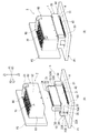
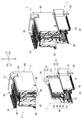
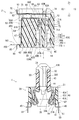
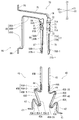
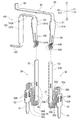
図1(A),(B)は、本発明の実施形態に係るプラグコネクタとこれに嵌合接続されるレセプタクルコネクタとを有するコネクタ組立体の外観斜視図であり、図1(A)は嵌合接続前、そして図1(B)は嵌合接続後の状態を示している。図2(A),(B)は、両コネクタ(プラグコネクタ及びレセプタクルコネクタ)の端子配列方向での信号端子の位置における断面斜視図であり、図2(A)は嵌合接続前、図2(B)は嵌合接続後の状態を、端子配列方向に対して直角な断面で示している。図3及び図4は、両コネクタの端子配列方向での信号端子の位置における断面図であり、図3は嵌合接続前、図4は嵌合接続後の状態を、端子配列方向に対して直角な断面で示している。   1A and 1B are external perspective views of a connector assembly having a plug connector according to an embodiment of the present invention and a receptacle connector fitted and connected to the plug connector, and FIG. FIG. 1B shows a state before the connection and after the connection. 2 (A) and 2 (B) are cross-sectional perspective views at the signal terminal positions in the terminal arrangement direction of both connectors (plug connector and receptacle connector), and FIG. (B) shows the state after fitting and connection in a cross section perpendicular to the terminal arrangement direction. 3 and 4 are cross-sectional views of the positions of the signal terminals in the terminal arrangement direction of both connectors. FIG. 3 shows the state before the mating connection, and FIG. 4 shows the state after the mating connection with respect to the terminal arrangement direction. The cross section is shown at right angles.

本実施形態では、プラグコネクタ1と該プラグコネクタに嵌合接続される相手コネクタ(相手接続体)としてのレセプタクルコネクタ2とでコネクタ組立体が構成されている。プラグコネクタ1及びレセプタクルコネクタ2は、それぞれ異なる回路基板へ実装される回路基板用電気コネクタである。   In the present embodiment, a connector assembly is constituted by the plug connector 1 and the receptacle connector 2 as a mating connector (mating connector) to be fitted and connected to the plug connector. The plug connector 1 and the receptacle connector 2 are electrical connectors for circuit boards that are mounted on different circuit boards.

図1に見られるように、プラグコネクタ1は、上下方向(Z軸方向)に直角な実装面をもつ回路基板P1上の該実装面に配され、レセプタクルコネクタ2は、コネクタ幅方向(X軸方向)に直角な実装面をもつ回路基板P2上の該実装面に配される。両コネクタは、図1(A),(B)に見られるように、回路基板P1と他の回路基板P2の実装面同士が互いに直角をなす姿勢のもとで、上下方向(Z軸方向)を接続方向として嵌合接続される。具体的には、図1(A),(B)に見られるように、プラグコネクタ1の上方からレセプタクルコネクタ2が嵌合接続されるようになっている。本実施形態では、レセプタクルコネクタ2がプラグコネクタ1の相手コネクタ(相手接続体)であるとしているが、レセプタクルコネクタ2からするとプラグコネクタ1が相手コネクタ(相手接続体)となることは言うまでもない。   As shown in FIG. 1, the plug connector 1 is arranged on the mounting surface on the circuit board P1 having a mounting surface perpendicular to the vertical direction (Z-axis direction), and the receptacle connector 2 is connected in the connector width direction (X-axis). The circuit board P2 having a mounting surface perpendicular to the direction). As shown in FIGS. 1 (A) and 1 (B), both connectors are arranged in the vertical direction (Z-axis direction) in a posture in which the mounting surfaces of the circuit board P1 and the other circuit board P2 are perpendicular to each other. The connection direction is fitted and connected. Specifically, as seen in FIGS. 1A and 1B, the receptacle connector 2 is fitted and connected from above the plug connector 1. In the present embodiment, the receptacle connector 2 is a mating connector (mating connector) of the plug connector 1, but it goes without saying that the plug connector 1 becomes a mating connector (mating connector) from the receptacle connector 2.

プラグコネクタ1は、上下方向(Z軸方向)をコネクタ高さ方向としており、回路基板P1の実装面に対して平行な一方向(Y軸方向)を長手方向として延びるプラグハウジング10と、該長手方向を端子配列方向としてプラグハウジング10に配列保持されるプラグ信号端子40およびプラグ電源端子50(以下、両者を区別する必要がないときは単に「プラグ端子40,50」という)とを有している。プラグ信号端子40は、端子配列方向(Y軸方向)でのプラグハウジング10の中間範囲に複数配列されており、プラグ電源端子50は、端子配列方向でのプラグ信号端子40の配列範囲の両側に設けられている。   The plug connector 1 has a plug housing 10 extending in the vertical direction (Z-axis direction) as a connector height direction and extending in one direction (Y-axis direction) parallel to the mounting surface of the circuit board P1 as a longitudinal direction. A plug signal terminal 40 and a plug power terminal 50 (hereinafter simply referred to as “plug terminals 40 and 50” when there is no need to distinguish between both) are arranged and held in the plug housing 10 with the direction as a terminal arrangement direction. Yes. A plurality of plug signal terminals 40 are arranged in an intermediate range of the plug housing 10 in the terminal arrangement direction (Y-axis direction), and the plug power supply terminals 50 are arranged on both sides of the arrangement range of the plug signal terminals 40 in the terminal arrangement direction. Is provided.

プラグハウジング10は、プラグ端子40,50を介して回路基板へ取り付けられる固定ハウジング20と、該固定ハウジング20とは別部材として形成され該固定ハウジング20に対して可動な可動ハウジング30とを有している。   The plug housing 10 includes a fixed housing 20 that is attached to a circuit board via plug terminals 40 and 50, and a movable housing 30 that is formed as a separate member from the fixed housing 20 and is movable with respect to the fixed housing 20. ing.

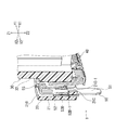
本実施形態では、プラグコネクタ1は回路基板P1の実装面に平行な方向をなし端子配列方向に対して直角なコネクタ幅方向(X軸方向)で対称に作られている。電気絶縁材料で作られた固定ハウジング20は、プラグコネクタ1の高さ方向である上下方向にて可動ハウジング30の下半部と重複する範囲をもって位置し、上下方向に見て可動ハウジング30の後述の嵌合部31を囲むように設けられており、端子配列方向(Y軸方向)を長手方向として延びる略直方体外形をなしている。   In the present embodiment, the plug connector 1 is formed symmetrically in the connector width direction (X-axis direction) that is parallel to the mounting surface of the circuit board P1 and perpendicular to the terminal arrangement direction. The fixed housing 20 made of an electrically insulating material is positioned with a range overlapping the lower half of the movable housing 30 in the vertical direction, which is the height direction of the plug connector 1, and will be described later. And has a substantially rectangular parallelepiped outer shape extending in the terminal arrangement direction (Y-axis direction) as the longitudinal direction.

固定ハウジング20は、図1(A),(B)に見られるように、端子配列方向で可動ハウジング30を含む範囲にわたって延びる二つの固定側側壁21と、コネクタ幅方向に延び固定側側壁21の端部同士を連結する二つの固定側端壁22とを有している。   As shown in FIGS. 1A and 1B, the fixed housing 20 includes two fixed side walls 21 extending over a range including the movable housing 30 in the terminal arrangement direction, and the fixed side wall 21 extending in the connector width direction. It has the two fixed side end walls 22 which connect edge parts.

固定側側壁21は、図1(A),(B)に見られるように、端子配列方向での両端部(プラグ電源端子50を含む範囲に位置する部分)が中間部(プラグ信号端子40の配列範囲を含んで位置する部分)よりも、外側面がコネクタ幅方向で外側に位置している。該固定側側壁21は、プラグ信号端子40の固定側被保持部42を圧入保持するための固定側信号端子保持部21A(図3参照)及びプラグ電源端子50の固定側被保持部52を圧入保持するための固定側電源端子保持部21B(図7参照)が、該固定側側壁21の内壁面に形成されている。   As shown in FIGS. 1A and 1B, the fixed side wall 21 has both end portions (portions located in a range including the plug power supply terminals 50) in the terminal arrangement direction in the middle portion (the plug signal terminal 40. The outer surface is located outside in the connector width direction than the portion including the arrangement range. The fixed side wall 21 press-fits the fixed-side signal terminal holding portion 21A (see FIG. 3) for press-fitting and holding the fixed-side held portion 42 of the plug signal terminal 40 and the fixed-side held portion 52 of the plug power supply terminal 50. A fixed power terminal holding portion 21 </ b> B (see FIG. 7) for holding is formed on the inner wall surface of the fixed side wall 21.

固定側信号端子保持部21Aは、図3に見られるように、固定側側壁21の下半部の内壁面から没するとともに下方へ開放された溝部として形成されている。また、固定側電源端子保持部21Bは、図7に見られるように、固定側側壁21の内壁面から没するとともに上下方向で固定側側壁21の全域にわたって延びる溝部として形成されている。また、固定側側壁21は、図7に見られるように、固定側電源端子保持部21Bの下部の両側縁部から端子配列方向(Y軸方向)で互いに近づくように突出する二つの被係止部21Cが形成されている。該被係止部21Cは、コネクタ幅方向及び端子配列方向に見て段状をなしており、その上面が、プラグ電源端子50の後述する係止部52Bに対して下方から係止可能な被係止面21C−1を形成している。   As shown in FIG. 3, the fixed-side signal terminal holding portion 21 </ b> A is formed as a groove portion that sinks from the inner wall surface of the lower half portion of the fixed-side side wall 21 and opens downward. Further, as shown in FIG. 7, the fixed-side power terminal holding portion 21 </ b> B is formed as a groove portion that sunk from the inner wall surface of the fixed-side side wall 21 and extends over the entire area of the fixed-side side wall 21 in the vertical direction. Further, as shown in FIG. 7, the fixed side wall 21 has two locked portions protruding from both side edge portions of the lower side of the fixed side power terminal holding portion 21 </ b> B so as to approach each other in the terminal arrangement direction (Y-axis direction). A portion 21C is formed. The locked portion 21C has a step shape when viewed in the connector width direction and the terminal arrangement direction, and the upper surface of the locked portion 21C can be locked from below with respect to a locking portion 52B described later of the plug power supply terminal 50. A locking surface 21C-1 is formed.

固定側端壁22は、コネクタ幅方向(X軸方向)中央域でその下半部が切り欠かれており、その壁厚方向(Y軸方向)に貫通するとともに下方へ開口した切欠部22Aが形成されている。固定側端壁22は、切欠部22Aの上方位置でコネクタ幅方向に延びる部分が、固定側側壁21の端部同士を連結する規制部22Bを形成している。該規制部22Bは、可動ハウジング30の後述する被規制部36の上方に位置しており、該規制部22Bの下面が、該被規制部36の上方への所定量以上の移動を規制する規制面22B−1として形成されている。   The lower half of the fixed end wall 22 is notched in the central region of the connector width direction (X-axis direction), and a notch 22A that penetrates in the wall thickness direction (Y-axis direction) and opens downward is provided. Is formed. In the fixed side end wall 22, a portion extending in the connector width direction above the notch 22 </ b> A forms a restricting portion 22 </ b> B that connects the ends of the fixed side wall 21. The restricting portion 22B is positioned above a later-described restricted portion 36 of the movable housing 30, and a lower surface of the restricting portion 22B restricts movement of a predetermined amount or more above the restricted portion 36. It is formed as a surface 22B-1.

可動ハウジング30は、固定ハウジング20と同様に電気絶縁材料で作られていて、レセプタクルコネクタ2との嵌合のための嵌合部31と、該固定ハウジング20から移動の規制を受ける被規制部36とを有している。嵌合部31は、端子配列方向に延びる二つの可動側側壁32と、コネクタ幅方向に延び可動側側壁32の端部同士を連結する二つの可動側端壁33とを有している。また、可動側側壁32及び可動側端壁33によって囲まれ上方へ開口する空間は、レセプタクルコネクタ2の後述の突壁65を受け入れるためのプラグ側受入部34として形成されている。該プラグ側受入部34の下端部は、図2(A),(B)及び図3に見られるように、端子配列方向で受入部34の全域にわたって延びる底壁35によって閉塞されている。   The movable housing 30 is made of an electrically insulating material as in the case of the fixed housing 20, and includes a fitting portion 31 for fitting with the receptacle connector 2, and a restricted portion 36 that is restricted from moving from the fixed housing 20. And have. The fitting part 31 has two movable side walls 32 extending in the terminal arrangement direction and two movable side end walls 33 extending in the connector width direction and connecting the ends of the movable side walls 32. A space that is surrounded by the movable side wall 32 and the movable side end wall 33 and opens upward is formed as a plug-side receiving portion 34 for receiving a later-described protruding wall 65 of the receptacle connector 2. As shown in FIGS. 2A, 2B and 3, the lower end of the plug-side receiving part 34 is closed by a bottom wall 35 extending over the entire area of the receiving part 34 in the terminal arrangement direction.

可動側側壁32は、端子配列方向におけるプラグ信号端子40の配列範囲では、プラグコネクタ1の上半部に対応する範囲で上下方向に延びており(図2(A),(B)参照)、端子配列方向での両端部(上記配列範囲よりも外側の部分)では、上下方向でのプラグコネクタ1のほぼ全域にわたる範囲で上下方向に延びている(図7参照)。   In the arrangement range of the plug signal terminals 40 in the terminal arrangement direction, the movable side wall 32 extends vertically in a range corresponding to the upper half of the plug connector 1 (see FIGS. 2A and 2B). At both end portions in the terminal arrangement direction (portions outside the arrangement range), the plug connector 1 extends in the vertical direction in the vertical direction (see FIG. 7).

可動側側壁32には、プラグ信号端子40の後述の信号用接触部43を収容するための収容溝部32Aが該可動側側壁32の内壁面に沿って形成されているとともに(図3参照)、プラグ電源端子50の後述の電源用接触部53を圧入保持するための収容溝部32B(図1(A)参照)が該可動側側壁32の外壁面に沿って形成されている。該収容溝部32Aは、可動側側壁32の内壁面から没するとともに上下方向に延びる直状の溝部として形成されている。一方、収容溝部32Bは、端子配列方向での可動側側壁32の両端部に位置しており、可動側側壁32の外壁面から没するとともに上下方向に延びる直状の溝部として形成されている。   On the movable side wall 32, an accommodation groove 32A for accommodating a later-described signal contact portion 43 of the plug signal terminal 40 is formed along the inner wall surface of the movable side wall 32 (see FIG. 3). A receiving groove 32B (see FIG. 1A) for press-fitting and holding a power contact portion 53 (described later) of the plug power terminal 50 is formed along the outer wall surface of the movable side wall 32. The housing groove portion 32A is formed as a straight groove portion that sunk from the inner wall surface of the movable side wall 32 and extends in the vertical direction. On the other hand, the accommodation groove 32B is located at both ends of the movable side wall 32 in the terminal arrangement direction, and is formed as a straight groove that extends from the outer wall surface of the movable side wall 32 and extends in the vertical direction.

可動側端壁33は、可動側側壁32の端子配列方向両端部と上下方向でほぼ同じ範囲、換言すると、上下方向でのプラグコネクタ1のほぼ全域にわたる範囲に延びている。底壁35は、プラグ信号端子40の可動側被保持部44を圧入保持する可動側信号端子保持部35Aが可動側側壁32の収容溝部32Aの直下に形成されているとともに、プラグ電源端子50の可動側被保持部54を圧入保持する可動側電源端子保持部(図示せず)が可動側側壁32の収容溝部32Bの直下に形成されている。可動側信号端子保持部35A及び可動側電源端子保持部は、上下方向に延びて底壁35を貫通する孔状をなしており、該可動側信号端子保持部35Aが収容溝部32Aと連通し、該可動側電源端子保持部が収容溝部32Bと連通している。   The movable-side end wall 33 extends in substantially the same range in the vertical direction as both ends of the movable-side side wall 32 in the terminal arrangement direction, in other words, in a range covering almost the entire region of the plug connector 1 in the vertical direction. The bottom wall 35 is formed with a movable side signal terminal holding portion 35A for press-fitting and holding the movable side held portion 44 of the plug signal terminal 40 directly below the receiving groove portion 32A of the movable side wall 32, and the plug power terminal 50 A movable side power terminal holding portion (not shown) for press-fitting and holding the movable side held portion 54 is formed immediately below the accommodating groove portion 32 </ b> B of the movable side wall 32. The movable-side signal terminal holding portion 35A and the movable-side power supply terminal holding portion have a hole shape extending in the vertical direction and penetrating the bottom wall 35, and the movable-side signal terminal holding portion 35A communicates with the accommodation groove portion 32A. The movable power supply terminal holding portion communicates with the accommodation groove portion 32B.

被規制部36は、可動ハウジング30の下部の端子配列方向両端面(端子配列方向に対して直角な面)から端子配列方向外方へ向けて突出している。該被規制部36は、図1(A),(B)に見られるように、角柱状をなしており、固定ハウジング20の固定側端壁22の切欠部22A内に端子配列方向内方から突入している。したがって、該被規制部36は、固定側端壁22の規制部22Bの直下に位置している。該被規制部36の上面(上下方向に対して直角な面)は、規制部22Bの下面である規制面22B−1と対面しており、該規制面22B−1と当接可能な被規制面36Aとして形成されている。該被規制面36Aは、上下方向で規制面22B−1に対して間隔をもって位置しているが、後述するように、可動ハウジング30が上方へ移動した際には、規制面22B−1に下方から当接(接面)する。その結果、可動ハウジング30の上方へ向けた所定量以上の移動が規制されるようになっている。   The regulated portion 36 protrudes outward in the terminal arrangement direction from both end faces (surfaces perpendicular to the terminal arrangement direction) of the lower part of the movable housing 30 in the terminal arrangement direction. As shown in FIGS. 1A and 1B, the regulated portion 36 has a prismatic shape, and enters the notch 22 </ b> A of the fixed side end wall 22 of the fixed housing 20 from the inside in the terminal arrangement direction. It has entered. Therefore, the regulated portion 36 is located directly below the regulating portion 22B of the fixed side wall 22. An upper surface (a surface perpendicular to the vertical direction) of the regulated portion 36 faces a regulating surface 22B-1 that is a lower surface of the regulating portion 22B, and is regulated so as to be able to contact the regulating surface 22B-1. It is formed as a surface 36A. The regulated surface 36A is positioned at an interval with respect to the regulating surface 22B-1 in the vertical direction. As will be described later, when the movable housing 30 moves upward, the regulated surface 22B is positioned below the regulating surface 22B-1. Abut (contact surface). As a result, movement of a predetermined amount or more upward of the movable housing 30 is restricted.

図1(A),(B)に見られるように、プラグコネクタ1では、プラグ端子40,50が二列をなして配列されており、各列において、複数のプラグ信号端子40が等間隔に配されているとともに、該プラグ信号端子40の配列範囲の両側にプラグ電源端子50が一つずつ配されている(図2(A),(B)をも参照)。   As shown in FIGS. 1A and 1B, in the plug connector 1, the plug terminals 40 and 50 are arranged in two rows, and a plurality of plug signal terminals 40 are equally spaced in each row. In addition, one plug power supply terminal 50 is arranged on each side of the arrangement range of the plug signal terminals 40 (see also FIGS. 2A and 2B).

プラグ信号端子40は、図2(A),(B)、図3及び図5に見られるように、金属帯状片をその板厚方向に屈曲して作られており、その端子幅方向(プラグ信号端子40の板厚方向に対して直角な方向)が端子配列方向(Y軸方向)と一致するように配されている。プラグ信号端子40は、プラグコネクタ1を端子配列方向に見たとき、図3に見られるように、下方に位置する一端部に形成された信号用接続部41と、該信号用接続部41から上方へ向けて延びる固定側被保持部42と、信号用接続部41よりも上方かつコネクタ幅方向内方に位置する他端部に形成された信号用接触部43と、該信号用接触部43から下方へ向けて延びる可動側被保持部44と、固定側被保持部42と可動側被保持部44とを連結する信号用弾性部45とを有している。該プラグ信号端子40は、コネクタ幅方向(X軸方向)で対称をなすように対をなして設けられていて、この対が端子配列方向(Y軸方向)に複数配列されている。   As shown in FIGS. 2A, 2B, 3 and 5, the plug signal terminal 40 is formed by bending a metal strip in the plate thickness direction. The signal terminals 40 are arranged so that the direction perpendicular to the plate thickness direction) coincides with the terminal arrangement direction (Y-axis direction). When the plug connector 1 is viewed in the terminal arrangement direction, the plug signal terminal 40 includes a signal connection portion 41 formed at one end located below and the signal connection portion 41 as seen in FIG. A fixed-side held portion 42 extending upward, a signal contact portion 43 formed at the other end located above the signal connection portion 41 and inward in the connector width direction, and the signal contact portion 43 A movable-side held portion 44 that extends downward from the bottom, and a signal elastic portion 45 that connects the fixed-side held portion 42 and the movable-side held portion 44. The plug signal terminals 40 are provided in pairs so as to be symmetrical in the connector width direction (X-axis direction), and a plurality of the pairs are arranged in the terminal arrangement direction (Y-axis direction).

信号用接続部41は、図3に見られるように、固定ハウジング20の底面より下方位置で、回路基板P1(図1(A),(B)参照)の実装面(上面)に位置するようにコネクタ幅方向外方に延びており、該実装面の対応回路部に半田接続されるようになっている。固定側被保持部42は、信号用接続部41のコネクタ幅方向での内側の端部で屈曲され上方へ向けて延びており、図3に見られるように、固定ハウジング20の固定側信号端子保持部21A内で圧入保持されている。具体的には、該固定側被保持部42は、図5に見られるように、端子幅方向(Y軸方向)での両側で上下方向に延びる側縁に複数の圧入突起42Aが形成されており、該圧入突起42Aが固定側信号端子保持部21Aの内壁面に喰い込むことにより保持されている。   As shown in FIG. 3, the signal connection portion 41 is positioned below the bottom surface of the fixed housing 20 and on the mounting surface (upper surface) of the circuit board P <b> 1 (see FIGS. 1A and 1B). The connector extends outward in the connector width direction and is soldered to the corresponding circuit portion of the mounting surface. The fixed side held portion 42 is bent at the inner end in the connector width direction of the signal connection portion 41 and extends upward, and as shown in FIG. 3, as shown in FIG. 3, the fixed side signal terminal of the fixed housing 20. It is press-fitted and held in the holding portion 21A. Specifically, as shown in FIG. 5, the fixed-side held portion 42 has a plurality of press-fitting protrusions 42 </ b> A formed on the side edges extending in the vertical direction on both sides in the terminal width direction (Y-axis direction). The press-fitting protrusion 42A is held by biting into the inner wall surface of the fixed-side signal terminal holding portion 21A.

一方、信号用接触部43は、図3に見られるように、可動ハウジング30の可動側側壁32の収容溝部32A内で該可動側側壁32の内壁面に沿って上下方向に延びている。該信号用接触部43は、一方の板面(板厚面に対して直角な面)がプラグ側受入部34へ向けて露呈しており、該板面が後述のレセプタクル信号端子70,80との接触のための接触面43Bを形成している。   On the other hand, as shown in FIG. 3, the signal contact portion 43 extends in the vertical direction along the inner wall surface of the movable side wall 32 in the housing groove portion 32 </ b> A of the movable side wall 32 of the movable housing 30. The signal contact portion 43 has one plate surface (a surface perpendicular to the plate thickness surface) exposed to the plug-side receiving portion 34, and the plate surface is connected to receptacle signal terminals 70 and 80 described later. The contact surface 43B for the contact of is formed.

可動側被保持部44は、図3に見られるように、信号用接触部43から連続して可動側信号端子保持部35A内で下方へ延びており、該可動側信号端子保持部35Aによって圧入保持されている。具体的には、該可動側被保持部44は、図5に見られるように、端子幅方向(Y軸方向)での両側で上下方向に延びる側縁に複数の圧入突起44Aが形成されており、該圧入突起44Aが可動側信号端子保持部35Aの内壁面に喰い込むことにより保持されている。   As shown in FIG. 3, the movable side held portion 44 continuously extends downward from the signal contact portion 43 in the movable side signal terminal holding portion 35A and is press-fitted by the movable side signal terminal holding portion 35A. Is retained. Specifically, as shown in FIG. 5, the movable side held portion 44 has a plurality of press-fitting protrusions 44A formed on the side edges extending in the vertical direction on both sides in the terminal width direction (Y-axis direction). The press-fitting protrusion 44A is held by biting into the inner wall surface of the movable signal terminal holding portion 35A.

信号用弾性部45は、図3ないし図5に見られるように、該信号用弾性部45の下端部で略U字状をなして湾曲する下側湾曲部45Aと、該信号用弾性部45の上端部で略逆U字状をなして湾曲する上側湾曲部45Bと、直状をなし該下側湾曲部45Aと上側湾曲部45Bとを連結する連結部45Cとを有しており、コネクタ幅方向(X軸方向)で弾性変位可能となっている。   As shown in FIGS. 3 to 5, the signal elastic portion 45 includes a lower curved portion 45 </ b> A that curves in a substantially U shape at the lower end portion of the signal elastic portion 45, and the signal elastic portion 45. An upper curved portion 45B which is curved in a substantially inverted U shape at the upper end portion thereof, and a connecting portion 45C which is straight and connects the lower curved portion 45A and the upper curved portion 45B. Elastic displacement is possible in the width direction (X-axis direction).

下側湾曲部45Aは、図5に見られるように、固定側被保持部42の上端で屈曲されて下方へ向かうにつれてコネクタ幅方向内方に傾斜するように延びる下側外腕部45A−1と、該下側外腕部45A−1の下端で折り返された下側折返部45A−2と、該下側折返部45A−2から上方へ向かうにつれてコネクタ幅方向外方に傾斜するように延びる下側内腕部45A−3とを有している。つまり、下側湾曲部45Aは、図3に見られるように、コネクタ幅方向で外側に傾斜した斜め上方へ開口する略U字状をなしている。該下側湾曲部45Aは、下側外腕部45A−1と下側内腕部45A−3とが互いの間隔を増減させるようにしてコネクタ幅方向で弾性変位可能となっている。   As shown in FIG. 5, the lower curved portion 45A is bent at the upper end of the fixed-side held portion 42 and extends so as to incline in the connector width direction as it goes downward. A lower folded portion 45A-2 folded at the lower end of the lower outer arm portion 45A-1, and extends so as to incline outward in the connector width direction from the lower folded portion 45A-2 upward. A lower inner arm 45A-3. That is, as shown in FIG. 3, the lower curved portion 45 </ b> A has a substantially U shape that opens obliquely upward and is inclined outward in the connector width direction. The lower curved portion 45A can be elastically displaced in the connector width direction so that the lower outer arm portion 45A-1 and the lower inner arm portion 45A-3 increase or decrease the distance between each other.

上側湾曲部45Bは、図5に見られるように、可動側被保持部44の下端で屈曲されて上方へ向かうにつれてコネクタ幅方向外方に傾斜するように延びる上側内腕部45B−1と、該上側内腕部45B−1の上端で折り返された上側折返部45B−2と、該上側折返部45B−2から下方へ向かうにつれてコネクタ幅方向内方に傾斜するように延びる上側外腕部45B−3とを有している。つまり、上側湾曲部45Bは、図3に見られるように、コネクタ幅方向で内側に傾斜した斜め下方へ開口する略逆U字状をなしている。該上側湾曲部45Bは、上側内腕部45B−1と上側外腕部45B−3とが互いの間隔を増減させるようにしてコネクタ幅方向で弾性変位可能となっている。   As shown in FIG. 5, the upper curved portion 45B is bent at the lower end of the movable side held portion 44 and extends upward so as to incline outward in the connector width direction. An upper folded portion 45B-2 folded at the upper end of the upper inner arm portion 45B-1, and an upper outer arm portion 45B extending so as to incline inward in the connector width direction downward from the upper folded portion 45B-2. -3. That is, as shown in FIG. 3, the upper curved portion 45B has a substantially inverted U-shape that opens obliquely downward and is inclined inward in the connector width direction. The upper curved portion 45B is elastically displaceable in the connector width direction so that the upper inner arm portion 45B-1 and the upper outer arm portion 45B-3 increase or decrease the distance between each other.

連結部45Cは、図3に見られるように、下側内腕部45A−3の上端と上側外腕部45B−3の下端とを連結して、下方へ向かうにつれてコネクタ幅方向内方に傾斜するように延びている。このように上下方向に対して傾斜して延びる連結部45Cは、図3に見られるように、コネクタ幅方向で下側湾曲部45Aの下側外腕部45A−1及び上側湾曲部45Bの上側内腕部45B−1と重複する範囲を有して位置している。したがって、この重複する範囲の分だけ、コネクタ幅方向で信号用弾性部45の寸法が小さくなるので、その結果、コネクタ幅方向でプラグコネクタ1を小型化することができる。   As shown in FIG. 3, the connecting portion 45C connects the upper end of the lower inner arm portion 45A-3 and the lower end of the upper outer arm portion 45B-3, and inclines inward in the connector width direction as it goes downward. It extends to do. Thus, as shown in FIG. 3, the connecting portion 45C extending obliquely with respect to the vertical direction is located above the lower outer arm portion 45A-1 and the upper curved portion 45B of the lower curved portion 45A in the connector width direction. It has a range that overlaps with the inner arm portion 45B-1. Accordingly, the size of the signal elastic portion 45 is reduced in the connector width direction by the overlapping range, and as a result, the plug connector 1 can be reduced in size in the connector width direction.

プラグ信号端子40では、信号用弾性部45の下側湾曲部45A及び上側湾曲部45Bがコネクタ幅方向で弾性変位することによりフローティングが行われるようになっている。また、本実施形態では、このように信号用弾性部45に下側湾曲部45A及び上側湾曲部45Bが設けられている分、該信号用弾性部45の全長が長くなり、フローティング量が大きくなる。   In the plug signal terminal 40, floating is performed by elastically displacing the lower curved portion 45A and the upper curved portion 45B of the signal elastic portion 45 in the connector width direction. In the present embodiment, the signal elastic portion 45 is thus provided with the lower curved portion 45A and the upper curved portion 45B, so that the entire length of the signal elastic portion 45 is increased and the floating amount is increased. .

図5に見られるように、下側湾曲部45Aの下側折返部45A−2は、その端子幅方向での中央域にて板厚方向に貫通するとともに該下側折返部45A−2の長手方向に延びるスリット状の下側孔部45A−2Aが形成されている。したがって、下側折返部45A−2は、下側外腕部45A−1及び下側内腕部45A−3よりも幅狭な二つの帯条片をなしており、これによって十分に大きい弾性が確保されている。また、上側湾曲部45Bの上側折返部45B−2においても、図5に見られるように、上述の下側折返部45A−2と同様のスリット状の上側孔部45B−2Aが形成されており、上側内腕部45B−1及び上側外腕部45B−3よりも幅狭な二つの帯条片によって十分に大きい弾性が確保されている。   As seen in FIG. 5, the lower folded portion 45A-2 of the lower curved portion 45A penetrates in the plate thickness direction in the center region in the terminal width direction and is the longitudinal length of the lower folded portion 45A-2. A slit-like lower hole 45A-2A extending in the direction is formed. Accordingly, the lower folded portion 45A-2 has two strips that are narrower than the lower outer arm portion 45A-1 and the lower inner arm portion 45A-3, and thereby has sufficiently large elasticity. It is secured. Also, in the upper folded portion 45B-2 of the upper curved portion 45B, a slit-like upper hole 45B-2A similar to the above-described lower folded portion 45A-2 is formed as shown in FIG. The sufficiently large elasticity is ensured by the two strips that are narrower than the upper inner arm portion 45B-1 and the upper outer arm portion 45B-3.

本実施形態では、図3及び図5に見られるように、プラグ信号端子40の下側湾曲部45A及び上側湾曲部45Bのそれぞれは、上下方向で重複して位置する部分をもつように湾曲している。具体的には、図5に見られるように、下側湾曲部45Aにおける下側外腕部45A−1と下側内腕部45A−3とが、そして、上側湾曲部45Bにおける上側内腕部45B−1と上側外腕部45B−3とが、互いに上下方向で重複する範囲をもって位置している。したがって、その重複している範囲の分だけ、上下方向における信号用弾性部45の寸法ひいてはプラグコネクタ1の寸法が小さくなり、プラグコネクタ1の低背化が図られる。   In this embodiment, as seen in FIGS. 3 and 5, each of the lower curved portion 45A and the upper curved portion 45B of the plug signal terminal 40 is curved so as to have a portion that is overlapped in the vertical direction. ing. Specifically, as seen in FIG. 5, the lower outer arm portion 45A-1 and the lower inner arm portion 45A-3 in the lower curved portion 45A, and the upper inner arm portion in the upper curved portion 45B. 45B-1 and the upper outer arm portion 45B-3 are positioned with a range overlapping each other in the vertical direction. Therefore, the dimension of the elastic signal portion 45 in the vertical direction and the dimension of the plug connector 1 are reduced by the overlapping range, and the height of the plug connector 1 is reduced.

本実施形態では、信号用弾性部45は、二つの湾曲部、すなわち下側湾曲部45A及び上側湾曲部45Bを有していることとしたが、これに代えて、下側湾曲部45A及び上側湾曲部45Bの一方のみを有していることとしてもよい。また、本実施形態では、湾曲部は信号用弾性部45の長手方向での端部に形成されていることとしたが、これに代えて、湾曲部は信号用弾性部45の長手方向での中間部に形成されていてもよい。このように信号用弾性部の一部に湾曲部を設けることにより、その分だけ、プラグコネクタ1の低背化が図られる。   In the present embodiment, the signal elastic portion 45 has two curved portions, that is, the lower curved portion 45A and the upper curved portion 45B. Instead, the lower curved portion 45A and the upper curved portion 45B are provided. It is good also as having only one of the curved parts 45B. In the present embodiment, the bending portion is formed at the end of the signal elastic portion 45 in the longitudinal direction. Instead, the bending portion is formed in the longitudinal direction of the signal elastic portion 45. You may form in the intermediate part. Thus, by providing a curved part in a part of the signal elastic part, the height of the plug connector 1 can be reduced by that much.

また、本実施形態では、信号用弾性部45はその全体で湾曲しているのではなく、プラグ信号端子40の長手方向での信号用弾性部45の一部、すなわち信号用弾性部45の下端部に形成された下側湾曲部45A及び上端部に形成された上側湾曲部45Bで湾曲している。したがって、信号用弾性部45全体を湾曲させる場合と比べて、湾曲部分(下側湾曲部45A及び上側湾曲部45B)における上下方向での重複部分の範囲が小さい。この結果、信号用弾性部45にてクロストークが生じにくくなり、高速伝送特性の低下を最小限に留めることができる。   In this embodiment, the signal elastic portion 45 is not curved as a whole, but a part of the signal elastic portion 45 in the longitudinal direction of the plug signal terminal 40, that is, the lower end of the signal elastic portion 45. It is curved by a lower curved portion 45A formed at the upper portion and an upper curved portion 45B formed at the upper end portion. Therefore, the range of the overlapping portion in the vertical direction in the curved portions (the lower curved portion 45A and the upper curved portion 45B) is smaller than when the entire signal elastic portion 45 is curved. As a result, crosstalk is less likely to occur in the signal elastic portion 45, and a reduction in high-speed transmission characteristics can be minimized.

本実施形態では、信号用弾性部45は、二つの湾曲部、すなわち下側湾曲部45A及び上側湾曲部45Bを有していることとしたが、これに代えて、下側湾曲部45A及び上側湾曲部45Bの一方のみを有していることとしてもよい。また、本実施形態では、湾曲部は信号用弾性部45の長手方向での端部に形成されていることとしたが、これに代えて、湾曲部は信号用弾性部45の長手方向での中間部に形成されていてもよい。このように信号用弾性部の一部に湾曲部を設けることにより、その分だけ、プラグコネクタ1の低背化が図られる。   In the present embodiment, the signal elastic portion 45 has two curved portions, that is, the lower curved portion 45A and the upper curved portion 45B. Instead, the lower curved portion 45A and the upper curved portion 45B are provided. It is good also as having only one of the curved parts 45B. In the present embodiment, the bending portion is formed at the end of the signal elastic portion 45 in the longitudinal direction. Instead, the bending portion is formed in the longitudinal direction of the signal elastic portion 45. You may form in the intermediate part. Thus, by providing a curved part in a part of the signal elastic part, the height of the plug connector 1 can be reduced by that much.

プラグ電源端子50は、図6に見られるように、金属帯状片をその板厚方向に屈曲して作られており、その端子幅方向(プラグ信号端子40の板厚方向に対して直角な方向)が端子配列方向(Y軸方向)と一致するように配されている。該プラグ電源端子50は、プラグ信号端子40よりも端子幅方向での寸法が大きく形成されている。   As shown in FIG. 6, the plug power supply terminal 50 is formed by bending a metal strip in the plate thickness direction, and its terminal width direction (a direction perpendicular to the plate thickness direction of the plug signal terminal 40). ) Is aligned with the terminal arrangement direction (Y-axis direction). The plug power supply terminal 50 is formed to have a larger dimension in the terminal width direction than the plug signal terminal 40.

プラグコネクタ1を端子配列方向に見たときに、プラグ電源端子50は、図6に見られるように、下方に位置する一端部に形成された電源用接続部51と、該電源用接続部51から上方へ向けて延びる固定側被保持部52と、電源用接続部51よりも上方かつコネクタ幅方向内方に位置する他端部に形成された電源用接触部53と、該電源用接触部53から下方へ向けて延びる可動側被保持部54と、固定側被保持部52と可動側被保持部54とを連結する電源用弾性部55とを有している。該プラグ電源端子50は、コネクタ幅方向(X軸方向)で対称をなすように対をなして設けられていて、この対が端子配列方向(Y軸方向)でのプラグコネクタ1の両端部で保持されている。   When the plug connector 1 is viewed in the terminal arrangement direction, as shown in FIG. 6, the plug power terminal 50 includes a power connection 51 formed at one end located below, and the power connection 51 A fixed-side held portion 52 extending upward from the power supply, a power contact portion 53 formed at the other end located above the power connection portion 51 and inward in the connector width direction, and the power contact portion The movable-side held portion 54 extends downward from 53, and the power-side elastic portion 55 that connects the fixed-side held portion 52 and the movable-side held portion 54. The plug power terminals 50 are provided in pairs so as to be symmetrical in the connector width direction (X-axis direction), and these pairs are provided at both ends of the plug connector 1 in the terminal arrangement direction (Y-axis direction). Is retained.

電源用接続部51は、固定ハウジング20の底面より下方位置で、上下方向で直状に延びている。該電源用接続部51は、プラグコネクタ1が回路基板P1(図1(A),(B)参照)の実装面に配された状態で、該回路基板P1に形成されたスルーホールH(図1(A),(B)参照)を上方から貫通して位置し、該スルーホールHに半田接続されるようになっている。該電源用接続部51は、図3に見られるように、プラグ信号端子40の信号用接続部41よりも、コネクタ幅方向での内側、換言すると、固定ハウジング20の固定側側壁21の壁厚方向(X軸方向)でプラグ信号端子40の信号用接触部43側に位置している。本実施形態では、電源用接続部51がこのように位置しているので、プラグコネクタ1がコネクタ幅方向で大型化することを回避できる。   The power supply connecting portion 51 extends straight in the vertical direction at a position below the bottom surface of the fixed housing 20. The power connection 51 includes a through hole H (see FIG. 1) formed in the circuit board P1 in a state where the plug connector 1 is arranged on the mounting surface of the circuit board P1 (see FIGS. 1A and 1B). 1 (A) and (B)) are penetrated from above and are connected to the through holes H by soldering. As shown in FIG. 3, the power connection 51 is located on the inner side in the connector width direction than the signal connection 41 of the plug signal terminal 40, in other words, the wall thickness of the fixed side wall 21 of the fixed housing 20. It is located on the signal contact portion 43 side of the plug signal terminal 40 in the direction (X-axis direction). In the present embodiment, since the power connection portion 51 is positioned in this way, it is possible to avoid the plug connector 1 from becoming large in the connector width direction.

固定側被保持部52は、電源用接続部51に連続して上方へ向けて延びており、固定ハウジング20の固定側電源端子保持部21B内で圧入保持されている(図7参照)。具体的には、図6に見られるように、該固定側被保持部52は、端子幅方向(Y軸方向)での両側で上下方向に延びる側縁に複数の圧入突起52Aが形成されており、該圧入突起52Aが固定側電源端子保持部21B(図7参照)の内壁面に喰い込むことにより保持されている。   The fixed-side held portion 52 extends upward continuously from the power connection portion 51 and is press-fitted and held in the fixed-side power terminal holding portion 21B of the fixed housing 20 (see FIG. 7). Specifically, as shown in FIG. 6, the fixed-side held portion 52 has a plurality of press-fitting protrusions 52 </ b> A formed on side edges extending in the vertical direction on both sides in the terminal width direction (Y-axis direction). The press-fitting protrusion 52A is held by biting into the inner wall surface of the fixed power terminal holding portion 21B (see FIG. 7).

本実施形態では、固定側被保持部52は、その板厚方向が固定ハウジング20の固定側側壁21の壁厚方向(X軸方向)と一致するように保持されているので、該固定側側壁21の壁厚方向での固定側被保持部52の寸法は該固定側被保持部52の板厚寸法であり小さい。したがって、固定側側壁21の壁厚を大きくすることなく該壁厚の範囲内に固定側被保持部52を位置させることができるので、プラグコネクタ1が上記壁厚方向で大型化することがない。   In the present embodiment, the fixed-side held portion 52 is held such that the plate thickness direction thereof coincides with the wall thickness direction (X-axis direction) of the fixed-side side wall 21 of the fixed housing 20. The dimension of the fixed side held part 52 in the wall thickness direction of 21 is the plate thickness dimension of the fixed side held part 52 and is small. Accordingly, the fixed-side held portion 52 can be positioned within the range of the wall thickness without increasing the wall thickness of the fixed-side side wall 21, so that the plug connector 1 is not increased in size in the wall thickness direction. .

また、固定側被保持部52は、端子幅方向での二位置にて、固定ハウジング20の被係止部21C(図7参照)に対して上方から係止可能な係止部52Bが設けられている。該係止部52Bは、固定側被保持部52の板面からコネクタ幅方向内方へ切り起こされた弾性片として形成されている。つまり、該係止部52Bは、下方へ向かうにつれてコネクタ幅方向内方へ向けて若干傾斜して延び、下端を自由端とする片持ち梁状をなしている。図7に見られるように、該係止部52Bの下端面は、上記被係止部21Cの上面である被係止面21C−1に対して直上に位置し、該被係止面21C−1に係止可能な係止面52B−1をなしている。   Further, the fixed-side held portion 52 is provided with a locking portion 52B that can be locked from above with respect to the locked portion 21C (see FIG. 7) of the fixed housing 20 at two positions in the terminal width direction. ing. The locking portion 52B is formed as an elastic piece cut and raised inward in the connector width direction from the plate surface of the fixed-side held portion 52. That is, the engaging portion 52B extends in a slightly inclined direction toward the inner side in the connector width direction as it goes downward, and has a cantilever shape with the lower end as a free end. As shown in FIG. 7, the lower end surface of the locking portion 52B is positioned directly above the locked surface 21C-1 that is the upper surface of the locked portion 21C, and the locked surface 21C- A locking surface 52B-1 that can be locked to 1 is formed.

後述するように、コネクタ抜出時にて固定ハウジング20に上方(コネクタ抜出方向)へ向けた外力が作用したとき、上方へもち上がった固定ハウジング20の被係止部21Cの被係止面21C−1に対して係止部52Bの係止面52B−1が上方から係止する。この結果、固定ハウジング20の上方へ向けた所定量以上の移動が規制されて、回路基板P1からプラグコネクタ1が外れることが良好に防止される。   As will be described later, when an external force directed upward (connector extraction direction) is applied to the fixed housing 20 when the connector is pulled out, the locked surface 21C of the locked portion 21C of the fixed housing 20 raised upward. The locking surface 52B-1 of the locking part 52B is locked from above with respect to -1. As a result, movement of a predetermined amount or more upward of the fixed housing 20 is restricted, and the plug connector 1 is favorably prevented from being detached from the circuit board P1.

本実施形態では、既述したように、係止部52Bは固定側被保持部52の板面から切り起こされた弾性片として形成されている。つまり、係止部52Bは、端子幅方向(Y軸方向)で該固定側被保持部52の範囲内に位置しているので、該端子幅方向で固定側被保持部52を大きくすることなく、係止部52Bにて十分な係止面積を確保できる。また、係止部52Bは端子幅方向での固定側被保持部52の範囲内に二つ形成されているので、係止部52Bを一つだけ形成する場合と比べて、上記係止面積を大きくすることができる。   In the present embodiment, as described above, the locking portion 52 </ b> B is formed as an elastic piece cut and raised from the plate surface of the fixed side held portion 52. That is, since the locking portion 52B is positioned within the range of the fixed side held portion 52 in the terminal width direction (Y-axis direction), the fixed side held portion 52 is not enlarged in the terminal width direction. A sufficient locking area can be secured by the locking portion 52B. Further, since the two locking portions 52B are formed within the range of the fixed-side held portion 52 in the terminal width direction, the locking area is reduced as compared with the case where only one locking portion 52B is formed. Can be bigger.

電源用接触部53は、可動ハウジング30の可動側側壁32の収容溝部32B内で該可動側側壁32の外壁面に沿って上下方向に延びている(図1(A)参照)。該電源用接触部53は、一方の板面(板厚面に対して直角な面)がコネクタ幅方向での外方へ向けて露呈しており、該板面がレセプタクル電源端子90,100との接触のための接触面53Aを形成している(図1(A)参照)。   The power contact portion 53 extends in the vertical direction along the outer wall surface of the movable side wall 32 in the housing groove 32B of the movable side wall 32 of the movable housing 30 (see FIG. 1A). In the power contact portion 53, one plate surface (a surface perpendicular to the plate thickness surface) is exposed outward in the connector width direction, and the plate surface is connected to the receptacle power supply terminals 90 and 100. A contact surface 53A is formed for contact (see FIG. 1A).

可動側被保持部54は、電源用接触部53から連続して可動側電源端子保持部(図示せず)内で下方へ延びており、該可動側電源端子保持部によって圧入保持されている。具体的には、図6に見られるように、該可動側被保持部54は、端子幅方向での両側で上下方向に延びる側縁に複数の圧入突起54Aが形成されており、該圧入突起54Aが可動側信号端子保持部の内壁面に喰い込むことにより保持されている。   The movable side held portion 54 continuously extends from the power contact portion 53 in a movable side power terminal holding portion (not shown), and is press-fitted and held by the movable side power terminal holding portion. Specifically, as shown in FIG. 6, the movable side held portion 54 has a plurality of press-fitting protrusions 54 </ b> A formed on the side edges extending in the vertical direction on both sides in the terminal width direction. 54A is held by biting into the inner wall surface of the movable signal terminal holding portion.

電源用弾性部55は、図6に見られるように、該電源用弾性部55の上端部で略逆U字状をなして湾曲する上側湾曲部55Aと、該電源用弾性部55の下端部で略U字状をなして湾曲する下側湾曲部55Bと、直状をなし該上側湾曲部55Aと下側湾曲部55Bとを連結する連結部55Cとを有しており、コネクタ幅方向で弾性変位可能となっている。   As shown in FIG. 6, the power supply elastic portion 55 includes an upper curved portion 55 </ b> A that curves in a substantially inverted U shape at the upper end portion of the power supply elastic portion 55, and a lower end portion of the power supply elastic portion 55. And has a lower curved portion 55B that is curved in a substantially U shape, and a connecting portion 55C that is straight and connects the upper curved portion 55A and the lower curved portion 55B. Elastic displacement is possible.

略逆U字状をなす上側湾曲部55A及び略U字状をなす下側湾曲部55Bは上下方向に沿って延びる二つの腕部を有している。該上側湾曲部55A及び該下側湾曲部55Bのそれぞれが該二つの腕部同士の間隔を増減させるようにしてコネクタ幅方向で弾性変位可能となっている。この結果、電源用弾性部55がコネクタ幅方向で弾性変位してフローティング可能となっている。   The upper curved portion 55A having a substantially inverted U shape and the lower curved portion 55B having a substantially U shape have two arm portions extending in the vertical direction. Each of the upper curved portion 55A and the lower curved portion 55B can be elastically displaced in the connector width direction so as to increase or decrease the distance between the two arm portions. As a result, the elastic portion for power supply 55 is elastically displaced in the connector width direction and can float.

連結部55Cは、図6に見られるように、上側湾曲部55Aのコネクタ幅方向内側の腕部の下端と下側湾曲部55Bのコネクタ幅方向外側の腕部の上端とを連結して、下方へ向かうにつれてコネクタ幅方向内方に傾斜するように延びている。   As shown in FIG. 6, the connecting portion 55C connects the lower end of the arm portion on the inner side in the connector width direction of the upper curved portion 55A and the upper end of the arm portion on the outer side in the connector width direction of the lower curved portion 55B. It extends so as to incline toward the inner side in the connector width direction.

電源用弾性部55は、図6に見られるように、上側湾曲部55Aのコネクタ幅方向外側の腕部及び折り返し部分(上端部)が幅狭に形成されているとともに、その他の部分が幅広に形成されている。幅狭の部分には、電源用弾性部55の長手方向に延びるスリット部55Dが形成されている。該スリット部55Dは電源用弾性部55の端子幅方向(Y軸方向)での中央域にて板厚方向に貫通している。つまり、上記幅狭の部分は二つの細条片で形成されている。また、幅広の部分には、電源用弾性部55の長手方向に延びる二つのスリット部55Eが形成されている。該二つのスリット部55Eは電源用弾性部55の端子幅方向(Y軸方向)での中間域における二位置で板厚方向に貫通している。つまり、上記幅広の部分は三つの細条片で形成されている。このように、電源用弾性部55は二つの細条片及び三つの細条片で形成されているので、十分に大きい弾性が確保されている。   As shown in FIG. 6, the power supply elastic portion 55 is formed such that the arm portion and the folded portion (upper end portion) on the outer side of the connector width direction of the upper curved portion 55 </ b> A are formed narrow, and the other portions are wide. Is formed. A slit portion 55D extending in the longitudinal direction of the power supply elastic portion 55 is formed in the narrow portion. The slit portion 55D penetrates in the plate thickness direction in the central region of the power supply elastic portion 55 in the terminal width direction (Y-axis direction). That is, the narrow portion is formed by two strips. Further, two slit portions 55E extending in the longitudinal direction of the power supply elastic portion 55 are formed in the wide portion. The two slit portions 55E penetrate in the plate thickness direction at two positions in the intermediate region in the terminal width direction (Y-axis direction) of the power supply elastic portion 55. That is, the wide part is formed of three strips. Thus, since the elastic part 55 for power supplies is formed with two strips and three strips, sufficiently large elasticity is ensured.

このような構成のプラグコネクタ1は、次の要領で製造される。まず、可動ハウジング30の可動側信号端子保持部35A及び可動側電源端子保持部35Bに、プラグ信号端子40の可動側被保持部44及びプラグ電源端子50の可動側被保持部54を上方へ向けて、すなわち可動ハウジング30の下側から圧入して、プラグ端子40,50を可動ハウジング30に保持させる。この結果、プラグ信号端子40の信号用接触部43及びプラグ電源端子50の電源用接触部53は、可動ハウジング30の収容溝部32A及び収容溝部32Bに収容される。   The plug connector 1 having such a configuration is manufactured in the following manner. First, the movable side held part 44 of the plug signal terminal 40 and the movable side held part 54 of the plug power terminal 50 are directed upward to the movable side signal terminal holding part 35A and the movable side power terminal holding part 35B of the movable housing 30. In other words, the plug terminals 40 and 50 are held in the movable housing 30 by press-fitting from the lower side of the movable housing 30. As a result, the signal contact portion 43 of the plug signal terminal 40 and the power contact portion 53 of the plug power supply terminal 50 are accommodated in the accommodation groove portion 32A and the accommodation groove portion 32B of the movable housing 30.

本実施形態では、プラグ電源端子50の電源用弾性部55は、端子配列方向に見たときの形状がプラグ信号端子40の信号用弾性部45と異なっているが、これに代えて、電源用弾性部を信号用弾性部45と同じ形状で形成してもよい。また、プラグコネクタにグランド端子を設ける場合には、該グランド端子に設けるグランド用弾性部を上記信号用弾性部45と同じ形状で形成してもよい。   In this embodiment, the power supply elastic portion 55 of the plug power supply terminal 50 is different from the signal elastic portion 45 of the plug signal terminal 40 in the shape when viewed in the terminal arrangement direction. The elastic portion may be formed in the same shape as the signal elastic portion 45. When the plug connector is provided with a ground terminal, the ground elastic portion provided on the ground terminal may be formed in the same shape as the signal elastic portion 45.

次に、固定ハウジング20の固定側信号端子保持部21A及び固定側電源端子保持部21Bに、プラグ信号端子40の固定側被保持部42及びプラグ電源端子50の固定側被保持部52を上方へ向けて、すなわち固定ハウジング20の下側から圧入して、プラグ端子40,50を固定ハウジング20に保持させる。このように、プラグ端子40,50を固定ハウジング20及び可動ハウジング30のそれぞれに取り付けることにより、プラグコネクタ1が完成する。   Next, the fixed-side held portion 42 of the plug signal terminal 40 and the fixed-side held portion 52 of the plug power terminal 50 are moved upward to the fixed-side signal terminal holding portion 21A and the fixed-side power supply terminal holding portion 21B of the fixed housing 20. The plug terminals 40 and 50 are held in the fixed housing 20 by being pressed in from the lower side of the fixed housing 20. Thus, the plug connector 1 is completed by attaching the plug terminals 40 and 50 to the fixed housing 20 and the movable housing 30, respectively.

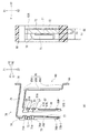
レセプタクルコネクタ2は、回路基板P2(図1(A),(B)参照)の実装面に対して平行な一方向(Y軸方向)を長手方向として延びるレセプタクルハウジング60と、該長手方向を端子配列方向としてレセプタクルハウジング60に配列保持されるレセプタクル信号端子70,80およびレセプタクル電源端子90,100(以下、両者を区別する必要がないときは単に「レセプタクル端子70,80,90,100」という)とを有している。レセプタクル信号端子70,80は、端子配列方向でのレセプタクルハウジング60の中間範囲に複数配列されており、レセプタクル電源端子90,100は、端子配列方向でのレセプタクル信号端子70,80の配列範囲の両側に設けられている。   The receptacle connector 2 includes a receptacle housing 60 extending in one direction (Y-axis direction) parallel to the mounting surface of the circuit board P2 (see FIGS. 1A and 1B) as a longitudinal direction, and the longitudinal direction as a terminal. Receptacle signal terminals 70 and 80 and receptacle power supply terminals 90 and 100 arranged and held in the receptacle housing 60 as the arrangement direction (hereinafter simply referred to as “receptacle terminals 70, 80, 90, 100” when there is no need to distinguish them) And have. A plurality of receptacle signal terminals 70 and 80 are arranged in the intermediate range of the receptacle housing 60 in the terminal arrangement direction, and the receptacle power supply terminals 90 and 100 are both sides of the arrangement range of the receptacle signal terminals 70 and 80 in the terminal arrangement direction. Is provided.

レセプタクルハウジング60は、端子配列方向での該レセプタクルハウジング60の両端位置で端子配列方向に対して直角な板面をもつ端壁61と、二つの該端壁61の間で端子配列方向に延びレセプタクル端子70,80,90,100を配列保持する中間部62とを有している。   The receptacle housing 60 has an end wall 61 having a plate surface perpendicular to the terminal arrangement direction at both end positions of the receptacle housing 60 in the terminal arrangement direction, and a receptacle extending between the two end walls 61 in the terminal arrangement direction. And an intermediate part 62 for holding the terminals 70, 80, 90, 100 in an array.

中間部62は、図1ないし図4に見られるように、その上端が端壁61の上端よりも下方に位置している。該中間部62は、図3におけるコネクタ幅方向(X軸方向)での略右半部(X1側の部分)に、レセプタクル信号端子70,80を収容して保持するためのレセプタクル信号端子収容部63が端子配列方向に配列形成されているとともに、該中間部62の両側位置でレセプタクル電源端子90,100を収容して保持するためのレセプタクル電源端子収容部(図示せず)が形成されている。また、図3におけるコネクタ幅方向(X軸方向)での略右半部(X1側の部分)は、その下半部に、プラグコネクタ10の嵌合部31を受け入れるためのレセプタクル側受入部64が下方に開口して形成されている(図3及び図4参照)。また、レセプタクル側受入部64内には、下方(Z2方向)へ向けて突出するとともに、端子配列方向(Y軸方向)へ延びる島状の突壁65が形成されている。   As shown in FIGS. 1 to 4, the intermediate portion 62 has an upper end positioned below the upper end of the end wall 61. The intermediate portion 62 is a receptacle signal terminal accommodating portion for accommodating and holding the receptacle signal terminals 70 and 80 in the substantially right half (X1 side portion) in the connector width direction (X axis direction) in FIG. 63 are arranged in the terminal arrangement direction, and receptacle power supply terminal receiving portions (not shown) for receiving and holding the receptacle power supply terminals 90 and 100 are formed at both side positions of the intermediate portion 62. . Further, the substantially right half (X1 side portion) in the connector width direction (X-axis direction) in FIG. 3 is a receptacle half receiving portion 64 for receiving the fitting portion 31 of the plug connector 10 in the lower half thereof. Is formed to open downward (see FIGS. 3 and 4). Further, in the receptacle-side receiving portion 64, an island-shaped protruding wall 65 is formed that protrudes downward (Z2 direction) and extends in the terminal arrangement direction (Y-axis direction).

レセプタクル信号端子収容部63及びレセプタクル電源端子収容部(図示せず)の形状の説明に先立ち、まず、レセプタクル信号端子70,80及びレセプタクル電源端子90,100の形状について説明する。   Prior to description of the shapes of the receptacle signal terminal accommodating portion 63 and the receptacle power supply terminal accommodating portion (not shown), first, the shapes of the receptacle signal terminals 70 and 80 and the receptacle power supply terminals 90 and 100 will be described.

レセプタクル信号端子70,80は、互いに形状の異なる第一レセプタクル信号端子70と第二レセプタクル信号端子80とを有している。本実施形態では、複数の第一レセプタクル信号端子70及び複数の第二レセプタクル信号端子80が、レセプタクルハウジング60の中間部62にて一列ずつ保持されている。   The receptacle signal terminals 70 and 80 have a first receptacle signal terminal 70 and a second receptacle signal terminal 80 having different shapes. In the present embodiment, the plurality of first receptacle signal terminals 70 and the plurality of second receptacle signal terminals 80 are held in a row at the intermediate portion 62 of the receptacle housing 60.

第一レセプタクル信号端子70は、図5に見られるように、金属板部材を板厚方向に屈曲して作られており、上下方向に延びる被保持部71と、該被保持部71の一方の板面から突出する第一当接部としての突部72と、該被保持部71の側縁にて他方の板面側に折り返されてコネクタ幅方向に延びる第二当接部としての舌片73と、該被保持部71の上部に連続する移行部74と、該移行部74の上端で屈曲されてコネクタ幅方向で回路基板P2側(X2側)へ向けて直状に延びる延長部75と、該延長部75の回路基板P2側の端部で屈曲されて上方へ向けて延びる信号用接続部76と、被保持部71の下端から下方へ向けて延びる接触腕部77,78とを有している。   As shown in FIG. 5, the first receptacle signal terminal 70 is formed by bending a metal plate member in the plate thickness direction, and includes a held portion 71 extending in the vertical direction and one of the held portions 71. A protrusion 72 as a first contact portion protruding from the plate surface, and a tongue piece as a second contact portion that is folded back to the other plate surface side at the side edge of the held portion 71 and extends in the connector width direction 73, a transition portion 74 continuous with the upper portion of the held portion 71, and an extension portion 75 that is bent at the upper end of the transition portion 74 and extends linearly toward the circuit board P2 side (X2 side) in the connector width direction. And a signal connection portion 76 that is bent at the end of the extension portion 75 on the circuit board P2 side and extends upward, and contact arm portions 77 and 78 that extend downward from the lower end of the held portion 71. Have.

被保持部71は、図3に見られるように、レセプタクルハウジング60の上端寄りに位置しており、該被保持部71の板厚方向が端子配列方向(図3の紙面に直角なY軸方向)と一致するように配されている。つまり、複数の第一レセプタクル信号端子70は、被保持部71同士の板面が端子配列方向で互いに対面するような姿勢で配列されている。該被保持部71は、上下方向に延びる二つの側縁のうちコネクタ幅方向でX1側に位置する側縁から突出する圧入突起71Aを、該被保持部71の上端寄り位置及び下端寄り位置に一つずつ有している。該被保持部71は、後述するように、レセプタクルハウジング60の第一信号端子保持部63Aの内壁面に圧入突起71Aが喰い込むことにより、該第一信号端子保持部63Aで保持されるようになっている。   As shown in FIG. 3, the held portion 71 is located near the upper end of the receptacle housing 60, and the thickness direction of the held portion 71 is in the terminal arrangement direction (the Y-axis direction perpendicular to the paper surface of FIG. 3). ) To match. That is, the plurality of first receptacle signal terminals 70 are arranged in such a posture that the plate surfaces of the held portions 71 face each other in the terminal arrangement direction. The held portion 71 has a press-fit projection 71A protruding from a side edge located on the X1 side in the connector width direction of two side edges extending in the vertical direction at a position closer to the upper end and lower end of the held portion 71. Have one by one. As will be described later, the held portion 71 is held by the first signal terminal holding portion 63A when the press-fitting protrusion 71A bites into the inner wall surface of the first signal terminal holding portion 63A of the receptacle housing 60. It has become.

突部72は、上下方向での二位置、具体的には圧入突起71Aとほぼ同位置にて、二つずつ形成されており、二つの該突部72はコネクタ幅方向(X軸方向)に配列されている。該突部72は、図5に見られるように、被保持部71の二つの板面のうち端子配列方向(Y軸方向)でのY2側に位置する一方の板面から突出するように、例えばエンボス加工により形成されている。つまり、該突部72は、該被保持部71の一方の板面よりもY2側に位置しており、Y軸方向で該一方の板面に対面する第一信号端子保持部63Aの内壁面(一方の内壁面)に対して近接して位置し、該突部72の突出頂面で当接可能となっている(図8(B)参照)。   Two protrusions 72 are formed at two positions in the vertical direction, specifically, at approximately the same position as the press-fitting protrusion 71A, and the two protrusions 72 are in the connector width direction (X-axis direction). It is arranged. As shown in FIG. 5, the protrusion 72 protrudes from one plate surface located on the Y2 side in the terminal arrangement direction (Y-axis direction) of the two plate surfaces of the held portion 71. For example, it is formed by embossing. That is, the protrusion 72 is located on the Y2 side of the one plate surface of the held portion 71, and the inner wall surface of the first signal terminal holding portion 63A that faces the one plate surface in the Y-axis direction. It is located close to (one inner wall surface) and can come into contact with the projecting top surface of the projection 72 (see FIG. 8B).

舌片73は、上下方向での圧入突起71A同士間の位置、換言すると上下方向での突部72同士間の位置に一つ形成されている。該舌片73は、被保持部71のX1側に位置する側縁、すなわち圧入突起71Aが形成されている側縁で該被保持部71の他方の板面側(Y1側)に折り返されて、コネクタ幅方向でX2側へ向けて延びている(図8(A)参照)。つまり、該舌片73は、上記被保持部71の他方の板面よりもY1側に位置しており、Y軸方向で該他方の板面に近接して対面する第一信号端子保持部63Aの内壁面(他方の内壁面)に対して近接して位置し、該舌片73の板面で当接可能となっている(図8(B)参照)。なお、本実施形態では、舌片73は、被保持部71の圧入突起71Aが形成されている側縁で折り返されて形成されていることとしたが、これに代えて、反対側の側縁で折り返されて形成されていてもよい。   One tongue piece 73 is formed at a position between the press-fitting protrusions 71A in the vertical direction, in other words, at a position between the protrusions 72 in the vertical direction. The tongue piece 73 is folded back to the other plate surface side (Y1 side) of the held portion 71 at the side edge located on the X1 side of the held portion 71, that is, the side edge where the press-fitting protrusion 71A is formed. , And extends toward the X2 side in the connector width direction (see FIG. 8A). That is, the tongue piece 73 is located on the Y1 side with respect to the other plate surface of the held portion 71, and faces the first signal terminal holding portion 63A facing the other plate surface in the Y-axis direction. It is located close to the inner wall surface (the other inner wall surface) and can be brought into contact with the plate surface of the tongue piece 73 (see FIG. 8B). In the present embodiment, the tongue piece 73 is formed by being folded back at the side edge where the press-fitting protrusion 71A of the held portion 71 is formed, but instead, the opposite side edge is formed. It may be formed by folding back.

移行部74及び延長部75は、レセプタクル信号端子収容部63の後述する上方収容部63E内に位置している。該移行部74は、図5及び図8(A)に見られるように、被保持部71の上部のX2側に位置する側縁でY1側へ直角に屈曲されてから上方へ向けて延びており、該移行部74の上端が被保持部71の上端よりも上方に位置している。また、延長部75は、移行部74の上端でX2側へ直角に屈曲されてX2側へ向けて延びている。   The transition part 74 and the extension part 75 are located in an upper accommodating part 63E, which will be described later, of the receptacle signal terminal accommodating part 63. As shown in FIGS. 5 and 8A, the transition portion 74 is bent at a right angle to the Y1 side at the side edge located on the X2 side of the upper portion of the held portion 71 and then extends upward. Thus, the upper end of the transition portion 74 is located above the upper end of the held portion 71. The extension portion 75 is bent at a right angle toward the X2 side at the upper end of the transition portion 74 and extends toward the X2 side.

信号用接続部76は、図3に見られるように、レセプタクルハウジング60外に位置しており、レセプタクルコネクタ2が回路基板P2の実装面に配された状態(図1参照)にて、該実装面上の対応信号回路部に接面し、半田接続されるようになっている。   As shown in FIG. 3, the signal connection portion 76 is located outside the receptacle housing 60, and the receptacle connector 2 is mounted on the mounting surface of the circuit board P2 (see FIG. 1). It contacts the corresponding signal circuit portion on the surface and is soldered.

二つの接触腕部77,78は、図5及び図8(A)に見られるように、長接触腕部77と、該長接触腕部77よりも腕長が短い短接触腕部78とを有しており、長接触腕部77の板面と短接触腕部78との板面が端子配列方向(Y軸方向)で板面が対面するように位置している。   As shown in FIGS. 5 and 8A, the two contact arm portions 77 and 78 include a long contact arm portion 77 and a short contact arm portion 78 having an arm length shorter than that of the long contact arm portion 77. The plate surface of the long contact arm portion 77 and the plate surface of the short contact arm portion 78 are positioned so that the plate surfaces face each other in the terminal arrangement direction (Y-axis direction).

長接触腕部77は、被保持部71の下端に連結された基部77Aと、該基部77Aから下方へ向けて延びる弾性腕部77Bとを有している。該弾性腕部77Bは、コネクタ幅方向(X軸方向)で、換言するとXZ平面内で弾性変位可能となっており、図3に見られるように、該弾性腕部77Bの下端部にてX1側へ突出してレセプタクルハウジング60のレセプタクル側受入部64内に位置する信号用接触部77B−1で、プラグコネクタ1のプラグ信号端子40に接圧をもって接触可能となっている(図4をも参照)。   The long contact arm portion 77 has a base portion 77A connected to the lower end of the held portion 71, and an elastic arm portion 77B extending downward from the base portion 77A. The elastic arm portion 77B is elastically displaceable in the connector width direction (X-axis direction), in other words, in the XZ plane, and as shown in FIG. 3, X1 is formed at the lower end portion of the elastic arm portion 77B. The signal contact portion 77B-1 that protrudes to the side and is located in the receptacle-side receiving portion 64 of the receptacle housing 60 can contact the plug signal terminal 40 of the plug connector 1 with contact pressure (see also FIG. 4). ).

短接触腕部78は、長接触腕部77の基部77AのX1側の側縁で折り返された基部78A(図8(A)参照)と、該基部78Aから下方へ向けて延びる弾性腕部78Bとを有している。該弾性腕部78Bは、長接触腕部77の弾性腕部77Bから独立してコネクタ幅方向(X軸方向)で、換言するとXZ平面内で弾性変位可能となっており、該弾性腕部78Bの下端部にてX1側へ突出してレセプタクルハウジング60のレセプタクル側受入部64内に位置する信号用接触部78B−1で、プラグコネクタ1のプラグ信号端子40に接圧をもって接触可能となっている(図4をも参照)。   The short contact arm portion 78 includes a base portion 78A (see FIG. 8A) that is folded at the side edge on the X1 side of the base portion 77A of the long contact arm portion 77, and an elastic arm portion 78B that extends downward from the base portion 78A. And have. The elastic arm portion 78B can be elastically displaced in the connector width direction (X-axis direction) independently of the elastic arm portion 77B of the long contact arm portion 77, in other words, in the XZ plane, and the elastic arm portion 78B. The signal contact portion 78B-1 that protrudes toward the X1 side at the lower end of the connector housing 60 and is located in the receptacle-side receiving portion 64 of the receptacle housing 60 can contact the plug signal terminal 40 of the plug connector 1 with contact pressure. (See also FIG. 4).

弾性腕部78Bは、図5に見られるように、長接触腕部77の弾性腕部77Bよりも腕長が短く、弾性腕部78Bの信号用接触部78B−1が弾性腕部77Bの信号用接触部77B−1よりもよりも若干上方に位置している(図8(A)をも参照)。したがって、レセプタクル信号端子70は、上下方向で互いに異なって位置する二つの信号用接触部77B−1,78B−1で、プラグ信号端子40に接触可能となっており、これによって、該プラグ信号端子40との接触の信頼性の向上が図られている。   As shown in FIG. 5, the elastic arm portion 78B has a shorter arm length than the elastic arm portion 77B of the long contact arm portion 77, and the signal contact portion 78B-1 of the elastic arm portion 78B is a signal of the elastic arm portion 77B. It is located slightly above the contact portion 77B-1 for use (see also FIG. 8A). Therefore, the receptacle signal terminal 70 can be brought into contact with the plug signal terminal 40 at the two signal contact portions 77B-1 and 78B-1 that are positioned differently in the vertical direction. The reliability of contact with 40 is improved.

第二レセプタクル信号端子80は、図3に見られるように、コネクタ幅方向(X軸方向)で第一レセプタクル信号端子70の被保持部71及び接触腕部77,78よりも回路基板P2側(X2側)に位置しているとともに、上下方向(Z軸方向)で第一レセプタクル信号端子70の延長部75よりも下方に位置している。   As shown in FIG. 3, the second receptacle signal terminal 80 is closer to the circuit board P2 side than the held portion 71 and the contact arm portions 77 and 78 of the first receptacle signal terminal 70 in the connector width direction (X-axis direction). X2 side) and is positioned below the extension 75 of the first receptacle signal terminal 70 in the vertical direction (Z-axis direction).

第二レセプタクル信号端子80は、図5に見られるように、上下方向に延びる被保持部81と、該被保持部81の一方の板面から突出する第一当接部としての突部82と、該被保持部81の側縁にて他方の板面側に折り返されてコネクタ幅方向に延びる第二当接部としての舌片83と、該被保持部81の上部に連続する移行部84と、該移行部84の上端で屈曲されてコネクタ幅方向で回路基板P2側(X2側)でクランク状に延びる延長部85と、該延長部85の回路基板P2側の端部で屈曲されて下方へ向けて延びる信号用接続部86と、被保持部81の下端から下方へ向けて延びる接触腕部87,88とを有している。   As shown in FIG. 5, the second receptacle signal terminal 80 includes a held portion 81 extending in the vertical direction, and a protruding portion 82 as a first abutting portion protruding from one plate surface of the held portion 81. A tongue piece 83 as a second abutting portion that is folded back to the other plate surface side at the side edge of the held portion 81 and extends in the connector width direction, and a transition portion 84 that is continuous with the upper portion of the held portion 81 An extension 85 that is bent at the upper end of the transition portion 84 and extends in a crank shape on the circuit board P2 side (X2 side) in the connector width direction, and is bent at an end of the extension 85 on the circuit board P2 side. The signal connecting portion 86 extends downward and the contact arm portions 87 and 88 extend downward from the lower end of the held portion 81.

被保持部81は、図3に見られるように、第一レセプタクル信号端子70の被保持部71よりも上下方向が小さく形成されており、該被保持部81の下端が該被保持部71の下端と上下方向でほぼ同じ高さに位置している。該被保持部81は、該被保持部81の板厚方向が端子配列方向と一致するように配されている。つまり、複数の第二レセプタクル信号端子80も、第一レセプタクル信号端子70と同様に、被保持部81同士の板面が端子配列方向で互いに対面するような姿勢で配列されている。該被保持部81は、上下方向に延びる二つの側縁のうちコネクタ幅方向でX2側に位置する側縁から突出する圧入突起81Aを、該被保持部81の上端寄り位置及び下端寄り位置に一つずつ有している。該被保持部81は、後述するように、レセプタクルハウジング60の第二信号端子保持部63Bの内壁面に圧入突起81Aが喰い込むことにより、該第二信号端子保持部63Bで保持されるようになっている。   As shown in FIG. 3, the held portion 81 is formed to be smaller in the vertical direction than the held portion 71 of the first receptacle signal terminal 70, and the lower end of the held portion 81 is the lower portion of the held portion 71. It is located at almost the same height at the bottom and up and down. The held portion 81 is arranged so that the plate thickness direction of the held portion 81 coincides with the terminal arrangement direction. That is, like the first receptacle signal terminal 70, the plurality of second receptacle signal terminals 80 are also arranged in such a posture that the plate surfaces of the held portions 81 face each other in the terminal arrangement direction. The held portion 81 has a press-fit projection 81A protruding from a side edge located on the X2 side in the connector width direction of two side edges extending in the vertical direction at a position closer to the upper end and lower end of the held portion 81. Have one by one. As will be described later, the held portion 81 is held by the second signal terminal holding portion 63B when the press-fitting protrusion 81A bites into the inner wall surface of the second signal terminal holding portion 63B of the receptacle housing 60. It has become.

突部82は、図8(A)に見られるように、上下方向での二位置、具体的には圧入突起81Aとほぼ同位置にて、二つずつ形成されており、二つの該突部82はコネクタ幅方向(X軸方向)に配列されている。該突部82は、被保持部81の二つの板面のうち端子配列方向(Y軸方向)でのY1側に位置する一方の板面から突出するように、例えばエンボス加工により形成されている。つまり、該突部82は、該被保持部81の一方の板面よりもY1側、すなわち第一レセプタクル信号端子70の突部72(図5参照)とはY軸方向にて反対側に位置しており、Y軸方向で該一方の板面に対面する第二信号端子保持部63Bの内壁面(一方の内壁面)に対して該突部82の突出頂面で当接可能となっている。   As shown in FIG. 8A, two protrusions 82 are formed at two positions in the vertical direction, specifically, at approximately the same position as the press-fitting protrusion 81A. 82 are arranged in the connector width direction (X-axis direction). The protrusion 82 is formed by, for example, embossing so as to protrude from one of the two plate surfaces of the held portion 81 located on the Y1 side in the terminal arrangement direction (Y-axis direction). . That is, the protrusion 82 is located on the Y1 side of one plate surface of the held portion 81, that is, on the opposite side in the Y-axis direction from the protrusion 72 (see FIG. 5) of the first receptacle signal terminal 70. The protrusion 82 can contact the inner wall surface (one inner wall surface) of the second signal terminal holding portion 63B facing the one plate surface in the Y-axis direction. Yes.

舌片83は、図8(A)に見られるように、上下方向での圧入突起81A同士間の位置、換言すると上下方向での突部82(図5参照)同士間の位置に一つ形成されている。該舌片83は、被保持部81のX2側に位置する側縁、すなわち圧入突起81Aが形成されている側縁で該被保持部81の他方の板面側(Y2側)に折り返されて、コネクタ幅方向でX1側へ向けて延びている。つまり、該舌片83は、上記被保持部81の他方の板面よりもY2側、すなわち第一レセプタクル信号端子70の舌片73とはY軸方向にて反対側に位置しており、Y軸方向で該他方の板面に対面する第二信号端子保持部63Bの内壁面(他方の内壁面)に対して該舌片83の板面で当接可能となっている。なお、本実施形態では、舌片83は、被保持部81の圧入突起81Aが形成されている側縁で折り返されて形成されていることとしたが、これに代えて、反対側の側縁で折り返されて形成されていてもよい。   As shown in FIG. 8A, one tongue piece 83 is formed at a position between the press-fitting protrusions 81A in the vertical direction, in other words, at a position between the protrusions 82 (see FIG. 5) in the vertical direction. Has been. The tongue 83 is folded back to the other plate surface side (Y2 side) of the held portion 81 at the side edge on the X2 side of the held portion 81, that is, the side edge where the press-fitting protrusion 81A is formed. , Extending toward the X1 side in the connector width direction. That is, the tongue piece 83 is located on the Y2 side from the other plate surface of the held portion 81, that is, on the opposite side to the tongue piece 73 of the first receptacle signal terminal 70 in the Y-axis direction. The plate surface of the tongue piece 83 can abut against the inner wall surface (the other inner wall surface) of the second signal terminal holding portion 63B facing the other plate surface in the axial direction. In the present embodiment, the tongue piece 83 is formed by being folded back at the side edge where the press-fitting protrusion 81A of the held portion 81 is formed, but instead, the opposite side edge is formed. It may be formed by folding back.

移行部84は、レセプタクル信号端子収容部63の第二信号端子保持部63B内に位置している。該移行部84は、図5に見られるように、被保持部81の上部のX2側に位置する側縁でY2側へ直角に屈曲されて形成されており、該移行部84の上端が上下方向で第一レセプタクル信号端子70の被保持部71の上端とほぼ同位置にある。   The transition portion 84 is located in the second signal terminal holding portion 63B of the receptacle signal terminal accommodating portion 63. As shown in FIG. 5, the transition portion 84 is formed by being bent at right angles to the Y2 side at the side edge located on the X2 side of the upper portion of the held portion 81, and the upper end of the transition portion 84 is vertically The first receptacle signal terminal 70 is substantially in the same position as the upper end of the held portion 71 in the direction.

延長部85は、図5に見られるように、移行部84の上端で直角に屈曲されてX2側へ向けて延びる上横部85Aと、該上横部85AのX2側の端部で直角に屈曲されて下方へ延びる縦部85Bと、該縦部85Bの下端で直角に屈曲されてX2側へ延びる下横部85Cとを有している。上横部85Aは、レセプタクル信号端子収容部63の後述する上方収容部63E内に位置しており、その長手方向(X軸方向)で第一レセプタクル信号端子70の延長部75よりも短くなっている(図3をも参照)。縦部85Bは、レセプタクル信号端子収容部63の後述する側方収容部63F内に位置している。下横部85Cは、図5に見られるように、X2側の端部がレセプタクルハウジング60外へ延出している。   As shown in FIG. 5, the extension 85 is bent at a right angle at the upper end of the transition portion 84 and extends toward the X2 side, and at a right angle at the end of the upper horizontal portion 85A on the X2 side. A vertical portion 85B that is bent and extends downward, and a lower horizontal portion 85C that is bent at a right angle at the lower end of the vertical portion 85B and extends toward the X2 side. The upper horizontal portion 85A is located in an upper accommodating portion 63E (described later) of the receptacle signal terminal accommodating portion 63, and is shorter than the extending portion 75 of the first receptacle signal terminal 70 in the longitudinal direction (X-axis direction). (See also FIG. 3). The vertical portion 85B is located in a side housing portion 63F, which will be described later, of the receptacle signal terminal housing portion 63. As shown in FIG. 5, the lower horizontal portion 85 </ b> C has an end portion on the X2 side extending out of the receptacle housing 60.

信号用接続部86は、図3(A),(B)に見られるように、レセプタクルハウジング60外にて、レセプタクル信号端子70の信号用接続部76とX軸方向で同位置にあり、レセプタクルコネクタ2が回路基板P2の実装面に配された状態にて、該実装面上の対応信号回路部に接面し、半田接続されるようになっている。   As shown in FIGS. 3A and 3B, the signal connection portion 86 is located at the same position in the X-axis direction as the signal connection portion 76 of the receptacle signal terminal 70 outside the receptacle housing 60. In a state where the connector 2 is arranged on the mounting surface of the circuit board P2, the corresponding signal circuit portion on the mounting surface is brought into contact with and soldered.

二つの接触腕部87,88は、図5及び図8(A)に見られるように、長接触腕部87と、該長接触腕部87よりも腕長が短い短接触腕部88とを有している。該接触腕部87,88は、既述したレセプタクル信号端子70の接触腕部77,78を、上下方向(Z軸方向)に延びる軸線まわりに180°回転させたような形状をなしている。接触腕部87,88自体の形状は、既述した接触腕部77,78の形状と同じなので、接触腕部87,88の各部については、接触腕部77,78で対応する部分の符号に「10」を加えた符号を付す(例えば、弾性腕部には符号「87B」、「88B」を付す)。   As shown in FIGS. 5 and 8A, the two contact arm portions 87 and 88 include a long contact arm portion 87 and a short contact arm portion 88 whose arm length is shorter than the long contact arm portion 87. Have. The contact arm portions 87 and 88 are shaped such that the contact arm portions 77 and 78 of the receptacle signal terminal 70 described above are rotated by 180 ° around an axis extending in the vertical direction (Z-axis direction). Since the shape of the contact arm portions 87 and 88 itself is the same as the shape of the contact arm portions 77 and 78 described above, the portions of the contact arm portions 87 and 88 are denoted by the corresponding reference numerals in the contact arm portions 77 and 78. A reference numeral added with “10” is attached (for example, reference numerals “87B” and “88B” are attached to the elastic arm portion).

長接触腕部87の信号用接触部87B−1は長接触腕部77の信号用接触部77B−1と、そして短接触腕部88の信号用接触部88B−1は短接触腕部78の信号用接触部78B−1と、上下方向で同位置に位置しておりX2方向へ向けて突出している。信号用接触部77B−1,78B−1は、レセプタクルハウジング60の受入部64内に位置しており、プラグコネクタ1のプラグ信号端子40に接圧をもって接触可能となっている(図4参照)。   The signal contact portion 87B-1 of the long contact arm portion 87 is the signal contact portion 77B-1 of the long contact arm portion 77, and the signal contact portion 88B-1 of the short contact arm portion 88 is the short contact arm portion 78. It is located at the same position in the vertical direction as the signal contact portion 78B-1, and protrudes in the X2 direction. The signal contact portions 77B-1 and 78B-1 are located in the receiving portion 64 of the receptacle housing 60, and can contact the plug signal terminal 40 of the plug connector 1 with contact pressure (see FIG. 4). .

レセプタクル電源端子90,100は、互いに形状の異なる第一レセプタクル電源端子90と第二レセプタクル電源端子100とを有している。本実施形態では、一つの第一レセプタクル電源端子90及び一つの第二レセプタクル電源端子100とから成る対が、レセプタクルハウジング60の中間部62の端子配列方向両側位置で一対ずつ保持されている。具体的には、レセプタクル電源端子90,100は、上記中間部62に形成されたレセプタクル電源端子収容部(図示せず)で収容保持されている。   The receptacle power supply terminals 90 and 100 have a first receptacle power supply terminal 90 and a second receptacle power supply terminal 100 having different shapes. In the present embodiment, a pair of one first receptacle power supply terminal 90 and one second receptacle power supply terminal 100 is held in pairs at both sides in the terminal arrangement direction of the intermediate portion 62 of the receptacle housing 60. Specifically, the receptacle power terminals 90 and 100 are accommodated and held in a receptacle power terminal accommodating portion (not shown) formed in the intermediate portion 62.

第一レセプタクル電源端子90は、図6に見られるように、金属板部材を板厚方向に屈曲して作られており、第一レセプタクル信号端子70よりも端子幅寸法(Y軸方向での寸法)が大きくなっている。該第一レセプタクル電源端子90は、上下方向に延びる被保持部91と、該被保持部91の上端から上方へ延びてから直角に屈曲されてコネクタ幅方向で回路基板P2側(X2側)へ向けて直状に延びる延長部92と、該延長部92の回路基板P2側の端部で屈曲されて上方へ向けて延びる電源用接続部93と、被保持部91の下端から下方へ向けて延びる二つの接触腕部94とを有している。第一レセプタクル電源端子90は、その端子幅方向が端子配列方向(Y軸方向)と一致するように配されている。   As shown in FIG. 6, the first receptacle power supply terminal 90 is formed by bending a metal plate member in the plate thickness direction, and the terminal width dimension (dimension in the Y-axis direction) is larger than the first receptacle signal terminal 70. ) Is getting bigger. The first receptacle power supply terminal 90 has a held portion 91 extending in the vertical direction, and extends upward from the upper end of the held portion 91 and then bent at a right angle to the circuit board P2 side (X2 side) in the connector width direction. An extension portion 92 that extends linearly toward the circuit board, a power supply connection portion 93 that is bent at the end portion of the extension portion 92 on the circuit board P2 side and extends upward, and downward from the lower end of the held portion 91. Two extending contact arm portions 94 are provided. The first receptacle power supply terminal 90 is arranged such that the terminal width direction thereof coincides with the terminal arrangement direction (Y-axis direction).

被保持部91は、レセプタクルハウジング60の上端寄りに位置しており、該被保持部91の板厚方向がコネクタ幅方向と一致するように配されている。該被保持部91は、上下方向に延びる端子幅方向(Y軸方向)での両側の側縁から突出する圧入突起91Aを、各側縁につき二つずつ有している。該被保持部91は、後述するように、レセプタクルハウジング60のレセプタクル電源端子収容部(図示せず)の一部をなす第一電源端子保持部(図示せず)の内壁面に圧入突起91Aが喰い込むことにより、該第一電源端子保持部で保持されるようになっている。   The held portion 91 is located near the upper end of the receptacle housing 60 and is arranged so that the plate thickness direction of the held portion 91 coincides with the connector width direction. The held portion 91 has two press-fitting protrusions 91A that protrude from the side edges on both sides in the terminal width direction (Y-axis direction) extending in the vertical direction. As will be described later, the held portion 91 has a press-fit projection 91A on the inner wall surface of a first power terminal holding portion (not shown) that forms a part of a receptacle power terminal housing portion (not shown) of the receptacle housing 60. By biting in, it is held by the first power terminal holding part.

延長部92は、図6に見られるように、その長手方向全体にわたって被保持部91よりも端子幅方向(Y軸方向)で幅狭に形成されている。該延長部92は、その長手方向にて被保持部91側に位置し横L字状に延びる部分が幅狭となっており、上記長手方向にて電源用接続部93側に位置し直状に延びる部分が幅広となっている。   As shown in FIG. 6, the extension portion 92 is formed narrower in the terminal width direction (Y-axis direction) than the held portion 91 over the entire longitudinal direction. The extension portion 92 is located on the held portion 91 side in the longitudinal direction and the portion extending in a horizontal L shape is narrow, and the extension portion 92 is located on the power supply connection portion 93 side in the longitudinal direction. The part extending to is wide.

電源用接続部93は、図3に見られるように、レセプタクルハウジング60外に位置しており、レセプタクルコネクタ2が回路基板P2の実装面に配された状態(図1参照)にて、該実装面上の対応電源回路部に接面し、半田接続されるようになっている。   As shown in FIG. 3, the power supply connecting portion 93 is located outside the receptacle housing 60, and the receptacle connector 2 is mounted on the mounting surface of the circuit board P2 (see FIG. 1). It contacts the corresponding power circuit section on the surface and is soldered.

二つの接触腕部94は、図6に見られるように、互いに同形状で形成されており、端子配列方向(Y軸方向)に配列されている。該接触腕部94は、下端寄り位置でX2側へ向けて突出するように屈曲されており、その突出した部分が、プラグコネクタ1のプラグ電源端子50に接圧をもって接触可能な電源用接触部94Aとして形成されている。図6に見られるように、二つの接触腕部94の電源用接触部94Aは上下方向で同位置に設けられている。また、該電源用接触部94Aは、図3に見られるように、第一レセプタクル信号端子70の信号用接触部77B−1,78B−1よりも上方でレセプタクルハウジング60のレセプタクル側受入部64内に突出して位置している。   As shown in FIG. 6, the two contact arm portions 94 are formed in the same shape as each other, and are arranged in the terminal arrangement direction (Y-axis direction). The contact arm portion 94 is bent so as to protrude toward the X2 side at a position near the lower end, and the protruding portion can contact the plug power supply terminal 50 of the plug connector 1 with a contact pressure. 94A. As shown in FIG. 6, the power contact portions 94A of the two contact arm portions 94 are provided at the same position in the vertical direction. Further, as shown in FIG. 3, the power contact portion 94A is located above the signal contact portions 77B-1 and 78B-1 of the first receptacle signal terminal 70 and in the receptacle side receiving portion 64 of the receptacle housing 60. It is located protruding.

第二レセプタクル電源端子100は、図6に見られるように、コネクタ幅方向(X軸方向)で第一レセプタクル電源端子90の被保持部91及び接触腕部94よりも回路基板P2側(X2側)に位置しているともに、上下方向(Z軸方向)で第一レセプタクル電源端子90の延長部92のコネクタ幅方向に延びる部分よりも下方に位置している。   As shown in FIG. 6, the second receptacle power supply terminal 100 is closer to the circuit board P2 side (X2 side) than the held portion 91 and the contact arm portion 94 of the first receptacle power supply terminal 90 in the connector width direction (X-axis direction). ) And in the vertical direction (Z-axis direction), it is located below the portion of the extension portion 92 of the first receptacle power supply terminal 90 extending in the connector width direction.

第二レセプタクル電源端子100は、図6に見られるように、金属板部材を板厚方向に屈曲して作られており、第二レセプタクル信号端子80よりも端子幅寸法(Y軸方向での寸法)が大きくなっている。該第二レセプタクル電源端子100は、上下方向に延びる被保持部101と、該被保持部101の上端からコネクタ幅方向で回路基板P2側(X2側)へ向けて直角に屈曲されてから下方へ向けて屈曲され直状に延びる延長部102と、該延長部102の回路基板P2側の下端で屈曲されて回路基板P2側(X2側)へ向けて延びる電源用接続部103と、被保持部101の下端から下方へ向けて延びる二つの接触腕部104とを有している。   As shown in FIG. 6, the second receptacle power supply terminal 100 is formed by bending a metal plate member in the plate thickness direction, and the terminal width dimension (dimension in the Y-axis direction) is larger than the second receptacle signal terminal 80. ) Is getting bigger. The second receptacle power supply terminal 100 includes a held portion 101 extending in the vertical direction, and bent downward at a right angle from the upper end of the held portion 101 toward the circuit board P2 side (X2 side) in the connector width direction. An extension portion 102 that is bent and extends straight, a power supply connection portion 103 that is bent at the lower end of the extension portion 102 on the circuit board P2 side and extends toward the circuit board P2 side (X2 side), and a held portion 101 and two contact arm portions 104 extending downward from the lower end of 101.

被保持部101及び接触腕部104は、既述した第一レセプタクル電源端子90の被保持部91及び接触腕部94と同じ上下方向位置で、該被保持部91及び該接触腕部94をコネクタ幅方向(X軸方向)で反転させた形状をなしている。該被保持部101及び接触腕部104の各部については、被保持部91及び接触腕部94の各部の符号に「10」を加えた符号を付すこととする(例えば、電源用接触部には符号「104A」を付す)。接触腕部104の電源用接触部104Aは、図3に見られるように、第二レセプタクル信号端子80の信号用接触部87B−1,88B−1よりも上方位置、かつ、第一レセプタクル電源端子90の電源用接触部94Aと同位置で、レセプタクルハウジング60のレセプタクル側受入部64内に突出している。   The held portion 101 and the contact arm portion 104 are connected to the held portion 91 and the contact arm portion 94 at the same vertical position as the held portion 91 and the contact arm portion 94 of the first receptacle power supply terminal 90 described above. The shape is reversed in the width direction (X-axis direction). About each part of this to-be-held part 101 and the contact arm part 104, the code | symbol which added "10" to the code | symbol of each part of the to-be-held part 91 and the contact arm part 94 shall be attached | subjected. Symbol “104A” is attached). As shown in FIG. 3, the power contact portion 104A of the contact arm portion 104 is positioned above the signal contact portions 87B-1 and 88B-1 of the second receptacle signal terminal 80, and the first receptacle power supply terminal. 90 protrudes into the receptacle-side receiving portion 64 of the receptacle housing 60 at the same position as the power supply contact portion 94A.

延長部102は、図6に見られるように、逆L字状に屈曲されており、その長手方向全体にわたって被保持部101よりも端子幅方向(Y軸方向)で幅狭に形成されている。該延長部102は、コネクタ幅方向(X軸方向)に延びる横部102Aと、上下方向(Z軸方向)に延びる縦部102Bとを有しており、該縦部102Bが上記横部102Aよりも幅広に形成されている。   As shown in FIG. 6, the extension portion 102 is bent in an inverted L shape, and is formed narrower in the terminal width direction (Y-axis direction) than the held portion 101 over the entire longitudinal direction. . The extension 102 has a horizontal portion 102A extending in the connector width direction (X-axis direction) and a vertical portion 102B extending in the vertical direction (Z-axis direction). The vertical portion 102B is more than the horizontal portion 102A. Is also formed wide.

電源用接続部103は、図3に見られるように、レセプタクルハウジング60外に位置しており、レセプタクルコネクタ2が回路基板P2の実装面に配された状態(図1参照)にて、該回路基板P2に形成されたスルーホール(図示せず)を貫通して位置し、該スルーホールに半田接続されるようになっている。   As shown in FIG. 3, the power supply connection portion 103 is located outside the receptacle housing 60, and in a state where the receptacle connector 2 is arranged on the mounting surface of the circuit board P2 (see FIG. 1), The through hole (not shown) formed in the substrate P2 is located through and is soldered to the through hole.

レセプタクルハウジング60の説明に戻る。レセプタクルハウジング60のレセプタクル信号端子収容部63は、図3に見られるように、レセプタクル信号端子70,80の被保持部71,81を保持するレセプタクル信号端子保持部63A,63B(第一信号端子保持部63A及び第二信号端子保持部63B)と、該レセプタクル信号端子70,80の接触腕部77,78の一部を収容する弾性変位許容溝部63C,63D(第一弾性変位許容溝部63Cと第二弾性変位許容溝部63D)と、第一レセプタクル信号端子70の延長部75及び第二レセプタクル信号端子80の延長部85の上横部85Aを収容する上方収容部63Eと、第二レセプタクル信号端子80の延長部85の縦部85Bを収容する側方収容部63Fとを有している。   Returning to the description of the receptacle housing 60. As shown in FIG. 3, the receptacle signal terminal accommodating portion 63 of the receptacle housing 60 has receptacle signal terminal holding portions 63A and 63B (first signal terminal holding portions) for holding the held portions 71 and 81 of the receptacle signal terminals 70 and 80. Part 63A and second signal terminal holding part 63B) and elastic displacement permissible groove parts 63C and 63D (first elastic displacement permissible groove part 63C and the first elastic displacement permissible groove part 63C) for accommodating part of contact arm parts 77 and 78 of the receptacle signal terminals 70 and 80 Two elastic displacement allowance grooves 63D), an upper accommodating portion 63E that accommodates an extension portion 75 of the first receptacle signal terminal 70 and an upper lateral portion 85A of the extension portion 85 of the second receptacle signal terminal 80, and a second receptacle signal terminal 80. Side extension portion 63 </ b> F for receiving the vertical portion 85 </ b> B of the extension portion 85.

レセプタクル信号端子保持部63A,63Bは、図3に見られるように、レセプタクルハウジング60の中間部62におけるコネクタ幅方向(X軸方向)での略右半部(X1側の部分)の上半部に形成されている。該レセプタクル信号端子保持部63A,63Bは、図3の紙面に対して直角な方向に拡がるとともに上下方向に延びて貫通するスリット状の孔部として形成されている。   As shown in FIG. 3, the receptacle signal terminal holding portions 63 </ b> A and 63 </ b> B are upper half portions of a substantially right half portion (X1 side portion) in the connector width direction (X-axis direction) in the intermediate portion 62 of the receptacle housing 60. Is formed. The receptacle signal terminal holding portions 63A and 63B are formed as slit-like holes that extend in a direction perpendicular to the paper surface of FIG.

レセプタクル信号端子保持部63A,63Bのうち、図3にてX1側に位置する第一信号端子保持部63Aは、図8(B)に見られるように、端子配列方向(Y軸方向)での幅寸法S1、換言すると、第一信号端子保持部63Aの内壁面同士の距離が、第一レセプタクル信号端子70の被保持部71の板厚寸法S2よりも大きく形成されている。また、該第一信号端子保持部63Aの上記幅寸法S1は、端子配列方向における第一レセプタクル信号端子70の突部72の突出頂面と舌片73の外側の板面(Y1側の板面)との距離S3よりも若干大きくなっている。   Of the receptacle signal terminal holding parts 63A and 63B, the first signal terminal holding part 63A located on the X1 side in FIG. 3 is in the terminal arrangement direction (Y-axis direction) as seen in FIG. 8B. The width dimension S1, in other words, the distance between the inner wall surfaces of the first signal terminal holding portion 63A is formed larger than the plate thickness dimension S2 of the held portion 71 of the first receptacle signal terminal 70. The width dimension S1 of the first signal terminal holding portion 63A is such that the protruding top surface of the protruding portion 72 of the first receptacle signal terminal 70 and the outer plate surface of the tongue piece 73 (the Y1 side plate surface) in the terminal arrangement direction. ) And a distance S3.

レセプタクル信号端子保持部63A,63Bのうち、図3にてX2側に位置する第二信号端子保持部63Bも、既述した第一信号端子保持部63Aと同様に、その幅寸法、換言すると、第二信号端子保持部63Bの内壁面同士の距離が、第二レセプタクル信号端子80の被保持部81の板厚寸法よりも大きく形成されている。また、上記幅寸法は、端子配列方向における第二レセプタクル信号端子80の突部82の突出頂面と舌片83の外側の板面(Y2側の板面)との距離よりも若干大きくなっている。   Of the receptacle signal terminal holding parts 63A and 63B, the second signal terminal holding part 63B located on the X2 side in FIG. 3 also has a width dimension, in other words, similar to the first signal terminal holding part 63A described above. The distance between the inner wall surfaces of the second signal terminal holding portion 63 </ b> B is formed to be larger than the plate thickness dimension of the held portion 81 of the second receptacle signal terminal 80. The width dimension is slightly larger than the distance between the protruding top surface of the protrusion 82 of the second receptacle signal terminal 80 and the outer plate surface of the tongue 83 (the plate surface on the Y2 side) in the terminal arrangement direction. Yes.

上述のような寸法関係のもとで、端子配列方向において、突部72,82の突出頂面とこれに対面する信号端子保持部63A,63Bの内壁面との間、そして、舌片73,83の上記板面とこれに対面する信号端子保持部63A,63Bの内壁面との間には、隙間が形成されている。このように、信号端子保持部63A,63Bの端子配列方向での寸法を若干大きく設定しておくことにより、レセプタクルハウジング60へのレセプタクル信号端子70,80の取付けの際に、被保持部71,81、突部72,82及び舌片73,83を信号端子保持部63A,63B内に容易にもたらすことができる。   Under the dimensional relationship as described above, in the terminal arrangement direction, between the projecting top surfaces of the projecting portions 72 and 82 and the inner wall surfaces of the signal terminal holding portions 63A and 63B facing each other, and the tongue pieces 73, A gap is formed between the plate surface 83 and the inner wall surfaces of the signal terminal holding portions 63A and 63B facing the plate surface. As described above, by setting the dimensions of the signal terminal holding portions 63A and 63B in the terminal arrangement direction to be slightly large, when the receptacle signal terminals 70 and 80 are attached to the receptacle housing 60, the held portions 71 and 81, the protrusions 72 and 82, and the tongue pieces 73 and 83 can be easily brought into the signal terminal holding portions 63A and 63B.

既述したように、本実施形態では、レセプタクル信号端子70,80の突部72,83及び舌片73,83が、信号端子保持部63A,63Bの内壁面に当接可能となっているので、突部72,83の突出頂面及び舌片73,83の板面と信号端子保持部63A,63Bの内壁面との間に隙間が存在していても、該信号端子保持部63A,63B内で被保持部71,81がその板厚方向(X軸方向)でほとんど傾斜することがなく正規位置で保持される。この結果、レセプタクル信号端子70,80全体も傾斜することがなく正規位置に維持されるので、プラグ信号端子40との良好な接触状態が確保され、信号伝送特性の低下を回避できる。   As described above, in the present embodiment, the protrusions 72 and 83 of the receptacle signal terminals 70 and 80 and the tongue pieces 73 and 83 can come into contact with the inner wall surfaces of the signal terminal holding portions 63A and 63B. Even if there are gaps between the protruding top surfaces of the protrusions 72 and 83 and the plate surfaces of the tongue pieces 73 and 83 and the inner wall surfaces of the signal terminal holding portions 63A and 63B, the signal terminal holding portions 63A and 63B. The held parts 71 and 81 are held at the normal position with almost no inclination in the thickness direction (X-axis direction). As a result, since the receptacle signal terminals 70 and 80 as a whole are not tilted and are maintained in the normal position, a good contact state with the plug signal terminal 40 is ensured, and deterioration in signal transmission characteristics can be avoided.

また、本実施形態では、突部72,82は被保持部71,81における上下方向での二位置に設けられている。このように突部72,82を上下方向での複数位置に設けることにより、信号端子保持部63A,63B内にて被保持部71,81をより安定させて正規位置に維持することができる。また、舌片73,83は、上下方向にて、互いに隣接する突部72,82の間の位置に設けられている。したがって、突部72,82及び被保持部71,81が上下方向で交互に配置され、これによって、信号端子保持部63A,63B内にて被保持部71,81をさらに確実に安定させて正規位置に維持することができる。   In the present embodiment, the protrusions 72 and 82 are provided at two positions in the vertical direction of the held portions 71 and 81. Thus, by providing the protrusions 72 and 82 at a plurality of positions in the vertical direction, the held parts 71 and 81 can be more stably maintained in the regular positions in the signal terminal holding parts 63A and 63B. Further, the tongue pieces 73 and 83 are provided at positions between the protrusions 72 and 82 adjacent to each other in the vertical direction. Therefore, the protrusions 72 and 82 and the held parts 71 and 81 are alternately arranged in the vertical direction, and thereby, the held parts 71 and 81 are more reliably stabilized in the signal terminal holding parts 63A and 63B. Can be maintained in position.

弾性変位許容溝部63C,63Dのうち、図3にてX1側に位置する第一弾性変位許容溝部63Cは、第一信号端子保持部63Aの下方にて上下方向に延びており、該第一信号端子保持部63Aと連通している。該第一弾性変位許容溝部63Cは、コネクタ幅方向にて突壁65のX1側に位置する側面から没するとともに上下方向に延びて貫通する溝状に形成されており、第一レセプタクル信号端子70の接触腕部77,78のX2側の部分を収容している。   Of the elastic displacement allowable groove portions 63C and 63D, the first elastic displacement allowable groove portion 63C located on the X1 side in FIG. 3 extends in the vertical direction below the first signal terminal holding portion 63A. It communicates with the terminal holding part 63A. The first elastic displacement permissible groove 63C is formed in a groove shape that sunk from the side surface located on the X1 side of the projecting wall 65 in the connector width direction and extends in the vertical direction and penetrates the first receptacle signal terminal 70. The contact arm portions 77 and 78 of the X2 side are housed.

第一弾性変位許容溝部63Cの溝底は、図3に見られるように、該第一弾性変位許容溝部63Cの上端から上下方向中間位置までの範囲では、下方へ向かうにつれてX2側へ傾斜するように延びており、該中間位置から下端までの範囲にでは、傾斜することなく下方へ延びている。したがって、上記溝底と接触腕部77,78との間には、コネクタ幅方向にて隙間が形成されている。第一弾性変位許容溝部63Cは、上記隙間によって接触腕部77,78の弾性変位を許容している。   As shown in FIG. 3, the groove bottom of the first elastic displacement allowable groove 63C is inclined toward the X2 side as it goes downward in the range from the upper end of the first elastic displacement allowable groove 63C to the middle position in the vertical direction. In the range from the intermediate position to the lower end, it extends downward without inclining. Accordingly, a gap is formed between the groove bottom and the contact arm portions 77 and 78 in the connector width direction. The first elastic displacement allowing groove 63 </ b> C allows the elastic displacement of the contact arm portions 77 and 78 by the gap.

弾性変位許容溝部63C,63Dのうち、図3にてX2側に位置する第二弾性変位許容溝部63Dは、既述した第一弾性変位許容溝部63Cをコネクタ幅方向で対称をなす形状で形成されている。該第二弾性変位許容溝部63Dは、第二レセプタクル信号端子80の接触腕部87,88のX1側の部分を収容している。また、該第二弾性変位許容溝部63Dは、コネクタ幅方向で第二弾性変位許容溝部63Dの溝底と接触腕部87,88との間に形成される隙間によって該接触腕部87,88の弾性変位を許容している。   Among the elastic displacement permissible groove portions 63C and 63D, the second elastic displacement permissible groove portion 63D located on the X2 side in FIG. 3 is formed in a shape that is symmetrical with the first elastic displacement permissible groove portion 63C described above in the connector width direction. ing. The second elastic displacement allowing groove 63 </ b> D accommodates the X <b> 1 side portion of the contact arm portions 87 and 88 of the second receptacle signal terminal 80. Further, the second elastic displacement allowance groove portion 63D is formed in the contact arm portions 87, 88 by a gap formed between the groove bottom of the second elastic displacement allowance groove portion 63D and the contact arm portions 87, 88 in the connector width direction. Elastic displacement is allowed.

上方収容部63Eは、端子配列方向(Y軸方向)でのレセプタクル信号端子70,80の位置にて、図3に見られるように、レセプタクルハウジング60の中間部62の上面から没するとともに、コネクタ幅方向(X軸方向)で第一信号端子保持部63Aの位置から上記中間部62の左端(X2側の端部)まで延びる範囲にわたって形成されている。端子配列方向で隣接する上方収容部63Eの間には、コネクタ幅方向での中間部62の左端側の位置で中間部62の上面から上方へ起立する上方隔壁66が形成されている。中間部62に形成された全ての上方収容部63Eは、端子配列方向に見て上方隔壁66を除いた範囲で端子配列方向に連通している。該上方収容部63E内に収容された第一レセプタクル信号端子70の延長部75及び第二レセプタクル信号端子80の延長部85の上横部85Aは、図3に見られるように、上下方向にて上方隔壁66の範囲内に位置している。その結果、延長部75及び上横部85Aは、上方隔壁66によって端子配列方向での移動が規制されている。   The upper accommodating portion 63E is submerged from the upper surface of the intermediate portion 62 of the receptacle housing 60 at the position of the receptacle signal terminals 70 and 80 in the terminal arrangement direction (Y-axis direction), as shown in FIG. It is formed over a range extending in the width direction (X-axis direction) from the position of the first signal terminal holding portion 63A to the left end (end on the X2 side) of the intermediate portion 62. Between the upper accommodating parts 63E adjacent in the terminal arrangement direction, an upper partition wall 66 is formed that rises upward from the upper surface of the intermediate part 62 at a position on the left end side of the intermediate part 62 in the connector width direction. All the upper accommodating portions 63E formed in the intermediate portion 62 communicate with each other in the terminal arrangement direction within a range excluding the upper partition wall 66 when viewed in the terminal arrangement direction. As shown in FIG. 3, the extension part 75 of the first receptacle signal terminal 70 and the upper horizontal part 85A of the extension part 85 of the second receptacle signal terminal 80 accommodated in the upper accommodation part 63E are arranged in the vertical direction. It is located within the range of the upper partition 66. As a result, the extension portion 75 and the upper horizontal portion 85A are restricted from moving in the terminal arrangement direction by the upper partition wall 66.

側方収容部63Fは、端子配列方向でのレセプタクル端子70,80の位置にて、図3に見られるように、レセプタクルハウジング60の中間部62のX2側の側面から没するとともに、上下方向にて上方収容部63Eの下端から上記中間部62の下端寄り位置まで延びる範囲にわたって形成されている。端子配列方向で隣接する側方収容部63Fの間には、中間部62の下端側の位置で中間部62の側面からX2側へ起立する側方隔壁67が形成されている。中間部62に形成された全ての側方収容部63Fは、端子配列方向に見て側方隔壁67を除いた範囲にて端子配列方向に連通している。該側方収容部63F内に収容された第二レセプタクル信号端子80の延長部85の縦部85Bは、図3に見られるように、コネクタ幅方向(X軸方向)にて側方隔壁67の範囲内に位置している。その結果、縦部85Bは、側方隔壁67によって端子配列方向での移動が規制されている。   As shown in FIG. 3, the side accommodating portion 63F is submerged from the side surface on the X2 side of the intermediate portion 62 of the receptacle housing 60 at the position of the receptacle terminals 70 and 80 in the terminal arrangement direction, and in the vertical direction. Thus, it is formed over a range extending from the lower end of the upper accommodating portion 63E to a position closer to the lower end of the intermediate portion 62. Between the side accommodating parts 63F adjacent in the terminal arrangement direction, a side partition wall 67 is formed that rises from the side surface of the intermediate part 62 to the X2 side at a position on the lower end side of the intermediate part 62. All the side accommodation parts 63F formed in the intermediate part 62 communicate with each other in the terminal arrangement direction in a range excluding the side partition walls 67 when viewed in the terminal arrangement direction. As shown in FIG. 3, the vertical portion 85B of the extension 85 of the second receptacle signal terminal 80 housed in the side housing portion 63F is formed by the side partition wall 67 in the connector width direction (X-axis direction). Located within range. As a result, the vertical portion 85 </ b> B is restricted from moving in the terminal arrangement direction by the side partition walls 67.

レセプタクルハウジング60のレセプタクル電源端子収容部(図示せず)は、レセプタクル電源端子90,100の被保持部91,101を保持するレセプタクル電源端子保持部と、該レセプタクル電源端子90,100の接触腕部94,104の一部を収容する弾性変位許容溝部と、第一レセプタクル電源端子90の延長部92及び第二レセプタクル電源端子100の延長部102の横部102Aを収容する上方収容部と、第二レセプタクル電源端子100の延長部102の縦部102Bを収容する側方収容部とを有している。   The receptacle power supply terminal accommodating portion (not shown) of the receptacle housing 60 includes a receptacle power supply terminal holding portion that holds the held portions 91 and 101 of the receptacle power supply terminals 90 and 100, and a contact arm portion of the receptacle power supply terminals 90 and 100. 94, 104 elastic displacement allowing groove, an upper receiving portion for receiving the extension portion 92 of the first receptacle power supply terminal 90 and the lateral portion 102A of the extension portion 102 of the second receptacle power supply terminal 100, and a second receiving portion. And a side accommodating portion that accommodates the vertical portion 102B of the extension 102 of the receptacle power supply terminal 100.

上記レセプタクル電源端子保持部及び該レセプタクル電源端子保持部の下方に位置する上記弾性変位許容溝部は、レセプタクルハウジング60のレセプタクル側受入部64を形成する内壁面のうち、コネクタ幅方向(X軸方向)にて突壁65の両側面と対面する二つの壁面(コネクタ幅方向で突壁65の両側に位置する壁面)から没して、上下方向に延びる溝状に形成されている。つまり、該二つの壁面のそれぞれにて、上記レセプタクル電源端子保持部と上記弾性変位許容溝部とが、上下方向に連続する一つの溝部をなしている。コネクタ幅方向でX1側に位置する該溝部では、第一レセプタクル電源端子90の被保持部91が圧入保持されるとともに、第一レセプタクル電源端子90の接触腕部94が弾性変位可能に収容される。一方、コネクタ幅方向でX2側に位置する該溝部では、第二レセプタクル電源端子100の被保持部101が圧入保持されるとともに、第二レセプタクル電源端子100の接触腕部104が弾性変位可能に収容される。   The receptacle power supply terminal holding portion and the elastic displacement allowing groove located below the receptacle power supply terminal holding portion are arranged in the connector width direction (X-axis direction) of the inner wall surface forming the receptacle-side receiving portion 64 of the receptacle housing 60. Are recessed from two wall surfaces (wall surfaces positioned on both sides of the protruding wall 65 in the connector width direction) facing the both side surfaces of the protruding wall 65, and are formed in a groove shape extending in the vertical direction. That is, in each of the two wall surfaces, the receptacle power terminal holding portion and the elastic displacement allowing groove portion form one groove portion that is continuous in the vertical direction. In the groove located on the X1 side in the connector width direction, the held portion 91 of the first receptacle power supply terminal 90 is press-fitted and held, and the contact arm portion 94 of the first receptacle power supply terminal 90 is accommodated so as to be elastically displaceable. . On the other hand, in the groove portion located on the X2 side in the connector width direction, the held portion 101 of the second receptacle power supply terminal 100 is press-fitted and held, and the contact arm portion 104 of the second receptacle power supply terminal 100 is accommodated in an elastically displaceable manner. Is done.

上記レセプタクル電源端子収容部の上記上方収容部及び上記側方収容部は、既述した上記レセプタクル信号端子収容部63の上方収容部63E及び側方収容部63Fを端子配列方向で幅広としたような形状をなしている。また、上記上方収容部及び上記側方収容部に収容されたレセプタクル電源端子90,100の延長部92,102は、既述したレセプタクル信号端子70,80と同様に、中間部62に設けられた隔壁によって端子配列方向での移動が規制されている。   The upper housing portion and the side housing portion of the receptacle power supply terminal housing portion are such that the upper housing portion 63E and the side housing portion 63F of the receptacle signal terminal housing portion 63 described above are wide in the terminal arrangement direction. It has a shape. Further, the extension portions 92 and 102 of the receptacle power supply terminals 90 and 100 accommodated in the upper accommodation portion and the side accommodation portion are provided in the intermediate portion 62 in the same manner as the receptacle signal terminals 70 and 80 described above. Movement in the terminal arrangement direction is regulated by the partition walls.

このような構成のレセプタクルコネクタ2は、次の要領で製造される。まず、レセプタクルハウジング60のレセプタクル信号端子収容部63へ第二レセプタクル信号端子80を上方から挿入する。この結果、第二レセプタクル信号端子80の被保持部81が第二信号端子保持部63Bに圧入され、該第二レセプタクル信号端子80がレセプタクル信号端子収容部63で収容保持される。   The receptacle connector 2 having such a configuration is manufactured in the following manner. First, the second receptacle signal terminal 80 is inserted into the receptacle signal terminal accommodating portion 63 of the receptacle housing 60 from above. As a result, the held portion 81 of the second receptacle signal terminal 80 is press-fitted into the second signal terminal holding portion 63B, and the second receptacle signal terminal 80 is received and held in the receptacle signal terminal holding portion 63.

また、レセプタクルハウジング60のレセプタクル電源端子収容部(図示せず)へ第二レセプタクル電源端子100を上方から挿入する。この結果、第二レセプタクル電源端子100の被保持部101がレセプタクル電源端子保持部に圧入され、第二レセプタクル電源端子100が上記レセプタクル電源端子収容部に収容保持される。   Further, the second receptacle power supply terminal 100 is inserted into the receptacle power supply terminal accommodating portion (not shown) of the receptacle housing 60 from above. As a result, the held portion 101 of the second receptacle power terminal 100 is press-fitted into the receptacle power terminal holding section, and the second receptacle power terminal 100 is housed and held in the receptacle power terminal housing section.

次に、レセプタクルハウジング60のレセプタクル信号端子収容部63へ第一レセプタクル信号端子70を上方から挿入する。この結果、第一レセプタクル信号端子70の被保持部71が第一信号端子保持部63Aに圧入され、該第一レセプタクル信号端子70がレセプタクル信号端子収容部63で収容保持される。   Next, the first receptacle signal terminal 70 is inserted into the receptacle signal terminal accommodating portion 63 of the receptacle housing 60 from above. As a result, the held portion 71 of the first receptacle signal terminal 70 is press-fitted into the first signal terminal holding portion 63 </ b> A, and the first receptacle signal terminal 70 is received and held in the receptacle signal terminal holding portion 63.

また、レセプタクルハウジング60のレセプタクル電源端子収容部(図示せず)へ第一レセプタクル電源端子90を上方から挿入する。この結果、第一レセプタクル電源端子90の被保持部91がレセプタクル電源端子保持部に圧入され、第一レセプタクル電源端子90が上記レセプタクル電源端子収容部に収容保持される。   Further, the first receptacle power supply terminal 90 is inserted into the receptacle power supply terminal accommodating portion (not shown) of the receptacle housing 60 from above. As a result, the held portion 91 of the first receptacle power terminal 90 is press-fitted into the receptacle power terminal holding section, and the first receptacle power terminal 90 is housed and held in the receptacle power terminal housing section.

このようにして、レセプタクル端子70,80,90,100をレセプタクルハウジング60に取り付けることによりレセプタクルコネクタ2が完成する。   In this way, the receptacle connector 2 is completed by attaching the receptacle terminals 70, 80, 90, 100 to the receptacle housing 60.

次に、プラグコネクタ1とレセプタクルコネクタ2との嵌合接続動作について説明する。まず、プラグコネクタ1を回路基板P1の実装面に半田接続して実装するとともに、レセプタクルコネクタ2を回路基板P2の実装面に半田接続して実装する。次に、図1及び図3に見られるように、プラグコネクタ1の嵌合部31が上方へ向いた姿勢で配置し、レセプタクルコネクタ2をレセプタクル側受入部64が下方に開口した姿勢にして、プラグコネクタ1の上方にもたらす。そして、レセプタクルコネクタ2を下方へ移動させることによりプラグコネクタ1との嵌合接続を開始する。   Next, the fitting and connecting operation between the plug connector 1 and the receptacle connector 2 will be described. First, the plug connector 1 is mounted by soldering on the mounting surface of the circuit board P1, and the receptacle connector 2 is mounted by soldering on the mounting surface of the circuit board P2. Next, as seen in FIGS. 1 and 3, the plug connector 1 is arranged with the fitting portion 31 facing upward, and the receptacle connector 2 is placed with the receptacle-side receiving portion 64 opened downward, Bring above the plug connector 1. Then, the receptacle connector 2 is moved downward to start fitting connection with the plug connector 1.

コネクタ嵌合過程では、プラグコネクタ1の嵌合部31がレセプタクルコネクタ2のレセプタクル側受入部64内へ下方から進入するとともに、レセプタクルコネクタ2の突壁65がプラグコネクタ1のプラグ側受入部34内へ上方から進入する。この結果、プラグコネクタ1のプラグ信号端子40の信号用接触部43が、レセプタクル信号端子70,80の信号用接触部77B−1,78B−1に当接して接触腕部77,78を弾性変位させる(図4参照)。また、プラグコネクタ1のプラグ電源端子50の信号用接触部53が、レセプタクル電源端子90,100の電源用接触部94A,104Aに当接して接触腕部94,104を弾性変位させる。   In the connector fitting process, the fitting portion 31 of the plug connector 1 enters the receptacle-side receiving portion 64 of the receptacle connector 2 from below, and the protruding wall 65 of the receptacle connector 2 is inside the plug-side receiving portion 34 of the plug connector 1. Enter from above. As a result, the signal contact portion 43 of the plug signal terminal 40 of the plug connector 1 abuts on the signal contact portions 77B-1 and 78B-1 of the receptacle signal terminals 70 and 80 to elastically displace the contact arm portions 77 and 78. (See FIG. 4). Further, the signal contact portion 53 of the plug power supply terminal 50 of the plug connector 1 contacts the power supply contact portions 94A and 104A of the receptacle power supply terminals 90 and 100 to elastically displace the contact arm portions 94 and 104.

さらに、コネクタ嵌合過程が進行し、図4に見られるように、プラグコネクタ1の嵌合部31がレセプタクルコネクタ2のレセプタクル側受入部64の奥部に到達するとともに、レセプタクルコネクタ2の突壁65がプラグコネクタ1のプラグ側受入部34の奥部に到達することにより、プラグコネクタ1とレセプタクルコネクタ2とが嵌合接続状態となり、コネクタ嵌合接続動作が完了する。コネクタ嵌合接続状態にて、レセプタクル信号端子70,80の接触腕部77,78の弾性変位状態は維持されており、プラグ信号端子40の信号用接触部43とレセプタクル信号端子70,80の信号用接触部77B−1,78B−1とが接圧をもって接触する。また、レセプタクル電源端子90,100の接触腕部94,104の弾性変位状態は維持されており、プラグ電源端子50の信号用接触部53とレセプタクル電源端子90,100の電源用接触部94A,104Aとが接圧をもって接触する。この結果、プラグ端子40,50とレセプタクル端子70,80,90,100とが電気的に導通する。   Further, the connector fitting process proceeds, and as shown in FIG. 4, the fitting portion 31 of the plug connector 1 reaches the back of the receptacle-side receiving portion 64 of the receptacle connector 2 and the protruding wall of the receptacle connector 2. When 65 reaches the depth of the plug-side receiving portion 34 of the plug connector 1, the plug connector 1 and the receptacle connector 2 are brought into a fitting connection state, and the connector fitting connection operation is completed. The elastic displacement state of the contact arm portions 77 and 78 of the receptacle signal terminals 70 and 80 is maintained in the connector fitting connection state, and the signal contact portion 43 of the plug signal terminal 40 and the signal of the receptacle signal terminals 70 and 80 are maintained. The contact portions 77B-1 and 78B-1 are brought into contact with each other with contact pressure. Further, the elastic displacement state of the contact arm portions 94 and 104 of the receptacle power supply terminals 90 and 100 is maintained, and the signal contact portion 53 of the plug power supply terminal 50 and the power supply contact portions 94A and 104A of the receptacle power supply terminals 90 and 100 are maintained. And contact with contact pressure. As a result, the plug terminals 40, 50 and the receptacle terminals 70, 80, 90, 100 are electrically connected.

コネクタ嵌合直前やコネクタ嵌合接続状態において、プラグコネクタ1とレセプタクルコネクタ2との嵌合位置が必ずしも端子配列方向及びコネクタ幅方向で正規位置となるとは限らず、これらの方向でずれることがある。本実施形態では、コネクタ1,2同士のずれは、プラグ端子40,50の弾性部45,55の弾性変位のもとで、可動ハウジング30がずれの方向へ向けて移動する、いわゆるフローティングにより吸収される。   Immediately before connector fitting or in the connector fitting connection state, the fitting position between the plug connector 1 and the receptacle connector 2 is not necessarily the normal position in the terminal arrangement direction and the connector width direction, and may be shifted in these directions. . In this embodiment, the displacement between the connectors 1 and 2 is absorbed by so-called floating in which the movable housing 30 moves in the direction of displacement under the elastic displacement of the elastic portions 45 and 55 of the plug terminals 40 and 50. Is done.

また、コネクタ抜出時にて、プラグコネクタ1に対して嵌合接続状態にあるレセプタクルコネクタ2をコネクタ抜出方向、すなわち上方(Z1方向)へもち上げると、プラグ端子40,50には、レセプタクル端子70,80,90,100との摩擦等に起因して上方へ向けた外力が作用する。この結果、プラグコネクタ1の可動ハウジング30は、プラグ端子40,50の弾性部45,55の弾性変位を伴いながら上方へ所定量移動するが、該可動ハウジング30の被規制部36の被規制面36Aが固定ハウジング20の規制部22Bの規制面22B−1に下方から当接することにより、該所定量以上の移動が規制される。したがって、固定ハウジング20ひいてはプラグ端子40,50がそれ以上もち上げられることはなく、回路基板P1の実装面からプラグ端子40,50の接続部41,51が剥離してプラグコネクタ1が外れることが防止される。   Further, when the receptacle connector 2 that is in the mating connection state with respect to the plug connector 1 is lifted in the connector extraction direction, that is, upward (Z1 direction) when the connector is extracted, the plug terminals 40 and 50 include the receptacle terminals. Due to friction with 70, 80, 90, 100, etc., an upward external force acts. As a result, the movable housing 30 of the plug connector 1 moves upward by a predetermined amount with the elastic displacement of the elastic portions 45 and 55 of the plug terminals 40 and 50, but the restricted surface of the restricted portion 36 of the movable housing 30. When 36A comes into contact with the restriction surface 22B-1 of the restriction portion 22B of the fixed housing 20 from below, the movement of the predetermined amount or more is restricted. Therefore, the fixed housing 20 and thus the plug terminals 40 and 50 are not lifted any further, and the connection portions 41 and 51 of the plug terminals 40 and 50 are peeled off from the mounting surface of the circuit board P1, and the plug connector 1 is detached. Is prevented.

しかし、可動ハウジング30の被規制部36の被規制面36Aが固定ハウジング20の規制部22Bの規制面22B−1に下方から当接する力が過剰に大きい合、固定ハウジング20が上方へもち上がってしまうおそれがある。本実施形態では、プラグ電源端子50の被保持部52が、固定ハウジング20の被係止部21Cに対して上下方向で係止可能な係止部52Bを有している。したがって、固定ハウジング20がもち上がってしまった場合であっても、プラグ電源端子50の係止部52Bの係止面52B−1が固定ハウジング20の被係止部21Cの被係止面21C−1に対して上方から当接して係止することにより、その係止力で、上方へ向けた上記外力に対抗することができる。この結果、回路基板P1の実装面からのプラグ端子40,50の接続部41,51の剥離ひいてはプラグコネクタ1の外れをより確実に防止できる。   However, if the force by which the regulated surface 36A of the regulated portion 36 of the movable housing 30 comes into contact with the regulating surface 22B-1 of the regulating portion 22B of the fixed housing 20 from below is excessively large, the fixed housing 20 rises upward. There is a risk that. In the present embodiment, the held portion 52 of the plug power supply terminal 50 has a locking portion 52B that can be locked in the vertical direction with respect to the locked portion 21C of the fixed housing 20. Therefore, even when the fixed housing 20 is lifted, the locking surface 52B-1 of the locking portion 52B of the plug power terminal 50 is locked to the locked surface 21C- of the locked portion 21C of the fixed housing 20. By abutting and engaging with 1 from above, the external force directed upward can be countered with the engaging force. As a result, the connection portions 41 and 51 of the plug terminals 40 and 50 from the mounting surface of the circuit board P1 can be more reliably prevented and the plug connector 1 can be prevented from coming off.

また、上記係止部52Bはプラグ電源端子50に設けられているので、従来のように、コネクタ抜出方向での外力に対抗するための金具を、端子配列範囲外に別途設ける必要がなく、プラグコネクタ1が端子配列方向で大型化することはない。   In addition, since the locking portion 52B is provided on the plug power supply terminal 50, there is no need to separately provide a metal fitting for countering external force in the connector pulling direction as in the prior art. The plug connector 1 does not increase in size in the terminal arrangement direction.

本実施形態では、プラグ電源端子50の係止部52Bは端子幅方向にて二つ設けられることとしたが、係止部の数はこれに限られず、例えば、三つ以上であってもよく、また、係止面の面積を十分に確保できるのであれば一つであってもよい。   In the present embodiment, the two locking portions 52B of the plug power supply terminal 50 are provided in the terminal width direction, but the number of the locking portions is not limited to this, and may be, for example, three or more. Moreover, one may be sufficient if the area of a latching surface can fully be ensured.

本実施形態では、レセプタクル信号端子70,80において、被保持部71,81の一方の板面側に設けられる第一当接部を突部72,82とし、他方の板面側に設けられる第二当接部を舌片73,83としたが、第一当接部及び第二当接部の形態はこれに限られない。例えば、第一当接部及び第二当接部の両方を突部としてもよく、また、第一当接部及び第二当接部の両方を舌片としてもよい。   In the present embodiment, in the receptacle signal terminals 70 and 80, the first abutting portions provided on one plate surface side of the held portions 71 and 81 are the projections 72 and 82, and the first contact portions provided on the other plate surface side. Although the two contact portions are the tongue pieces 73 and 83, the form of the first contact portion and the second contact portion is not limited to this. For example, both the first contact portion and the second contact portion may be protrusions, and both the first contact portion and the second contact portion may be tongue pieces.

また、本実施形態では、上下方向での各位置につき二つずつ設けられていることとしたが、突部の数はこれに限られず、一つであってもよく、三つ以上であってもよい。また、上下方向での各位置に突部を一つだけ設ける場合には、該突部を被保持部の幅方向(X軸方向)に延びた形状としてもよい。このような形状とすることにより該突部の突出頂面の面積、換言すると、端子保持部の内壁面に当接可能な面積を大きくすることができ、レセプタクル信号端子の姿勢をより安定させやすくなる。   In the present embodiment, two are provided for each position in the vertical direction. However, the number of protrusions is not limited to this, and may be one, or three or more. Also good. When only one protrusion is provided at each position in the vertical direction, the protrusion may have a shape extending in the width direction (X-axis direction) of the held portion. By adopting such a shape, the area of the protruding top surface of the protrusion, in other words, the area that can contact the inner wall surface of the terminal holding portion can be increased, and the attitude of the receptacle signal terminal can be made more stable. Become.

本実施形態では、突部72,82が上下方向での二箇所に設けられ、舌片73,83が上下方向での一箇所に設けられることとしたが、突部及び舌片を設ける上下方向での位置の数はこれに限られず、さらに増やしてもよい。これによって、レセプタクル信号端子の姿勢をよりさらに安定させやすくなる。   In this embodiment, the protrusions 72 and 82 are provided at two locations in the vertical direction, and the tongue pieces 73 and 83 are provided at one location in the vertical direction. However, the vertical direction in which the protrusions and the tongue pieces are provided. The number of positions at is not limited to this, and may be further increased. This makes it easier to stabilize the attitude of the receptacle signal terminal.

1 プラグコネクタ 53 電源用接触部
2 レセプタクルコネクタ 60 レセプタクルハウジング
10 プラグハウジング 63A 第一信号端子保持部
20 固定ハウジング 63B 第二信号端子保持部
21C 被係止部 70 第一レセプタクル信号端子
22 固定側端壁 71 被保持部
30 可動ハウジング 72 突部(第一当接部)
40 プラグ信号端子 73 舌片(第二当接部)
41 信号用接続部 77 長接触腕部
42 固定側被保持部 77B−1 信号用接触部
43 信号用接触部 78 短接触腕部
44 可動側被保持部 78B−1 信号用接触部
45 信号用弾性部 80 第二レセプタクル信号端子
45A 下側湾曲部 81 被保持部
45B 上側湾曲部 82 突部(第一当接部)
50 プラグ電源端子 83 舌片(第二当接部)
51 電源用接続部 P1 回路基板
52 固定側被保持部 P2 回路基板
52B 係止部
DESCRIPTION OF SYMBOLS 1 Plug connector 53 Contact part for power supplies 2 Receptacle connector 60 Receptacle housing 10 Plug housing 63A 1st signal terminal holding | maintenance part 20 Fixed housing 63B 2nd signal terminal holding | maintenance part 21C Locked part 70 1st receptacle signal terminal 22 Fixed side end wall 71 Hold portion 30 Movable housing 72 Projection (first contact portion)
40 Plug signal terminal 73 Tongue piece (second contact part)
41 Signal connection portion 77 Long contact arm portion 42 Fixed side held portion 77B-1 Signal contact portion 43 Signal contact portion 78 Short contact arm portion 44 Movable side held portion 78B-1 Signal contact portion 45 Signal elasticity Part 80 Second receptacle signal terminal 45A Lower curved part 81 Hold part 45B Upper curved part 82 Projection (first contact part)
50 Plug power supply terminal 83 Tongue piece (second contact part)
51 Power supply connection part P1 Circuit board 52 Fixed side held part P2 Circuit board 52B Locking part

Claims (5)

回路基板の実装面に配される回路基板用電気コネクタであって、
上記実装面に対して平行な一方向を配列方向として配列される金属板製の複数の端子と、該複数の端子を配列保持するハウジングとを有し、
上記ハウジングは、上記実装面に対して直角なコネクタ高さ方向に起立するとともに上記配列方向に延びる側壁を有し、
上記複数の端子は、信号端子と電源端子とを有し、
該電源端子は、上記側壁に保持される被保持部を有し、
該被保持部は、該被保持部の板厚方向に対して直角な端子幅方向での両側縁で上記側壁により圧入保持されている回路基板用電気コネクタにおいて、
上記側壁は、上記電源端子の被保持部と対応する位置に段状の被係止部を有し、
上記電源端子の被保持部は、上記被係止部に対してコネクタ高さ方向で係止可能な係止部を有していることを特徴とする回路基板用電気コネクタ。
An electrical connector for a circuit board disposed on the mounting surface of the circuit board,
A plurality of terminals made of a metal plate arranged with the direction parallel to the mounting surface as an arrangement direction, and a housing that holds the plurality of terminals arranged;
The housing has side walls that stand in the connector height direction perpendicular to the mounting surface and extend in the arrangement direction,
The plurality of terminals have a signal terminal and a power supply terminal,
The power supply terminal has a held portion held on the side wall,
In the electrical connector for a circuit board, the held portion is press-fitted and held by the side wall at both side edges in the terminal width direction perpendicular to the plate thickness direction of the held portion.
The side wall has a stepped locked portion at a position corresponding to the held portion of the power terminal,
The circuit board electrical connector according to claim 1, wherein the held portion of the power supply terminal has a locking portion that can be locked to the locked portion in the connector height direction.
上記係止部は、上記被保持部の板面から切り起こされた弾性片として形成されていることとする請求項1に記載の回路基板用電気コネクタ。   The circuit board electrical connector according to claim 1, wherein the locking portion is formed as an elastic piece cut and raised from a plate surface of the held portion. 上記電源端子は、板厚方向に屈曲した形状をなしており、上記被保持部の板厚方向が上記ハウジングの側壁の壁厚方向と一致するようにして該側壁に保持されていることとする請求項1又は請求項2に記載の回路基板用電気コネクタ。   The power supply terminal has a shape bent in the plate thickness direction, and is held by the side wall so that the plate thickness direction of the held portion coincides with the wall thickness direction of the side wall of the housing. The electrical connector for circuit boards according to claim 1 or 2. 上記被保持部は、端子幅方向での該被保持部の範囲内に複数形成されていることとする請求項1ないし請求項3のいずれかに記載の回路基板用電気コネクタ。   4. The circuit board electrical connector according to claim 1, wherein a plurality of the held parts are formed within a range of the held parts in the terminal width direction. 上記端子は、該端子の長手方向の一端側に回路基板の実装面への接続のための接続部そして他端側に相手接続体との接触のための接触部が形成されており、
上記接続部と上記接触部とは、上記ハウジングの側壁の壁厚方向で異なって位置しており、
上記電源端子の接続部は、上記信号端子の接続部よりも、上記側壁の壁厚方向で該信号端子の接触部側に位置していることとする請求項1ないし請求項4のいずれかに記載の回路基板用電気コネクタ。
The terminal has a connection part for connection to the mounting surface of the circuit board on one end side in the longitudinal direction of the terminal and a contact part for contact with the mating connector on the other end side,
The connection portion and the contact portion are located differently in the wall thickness direction of the side wall of the housing,
The connection part of the said power supply terminal is located in the contact part side of this signal terminal in the wall thickness direction of the said side wall rather than the connection part of the said signal terminal. The electrical connector for circuit boards as described.
JP2018085155A 2018-04-26 2018-04-26 Circuit board electrical connector Pending JP2019192527A (en)

Priority Applications (6)

Application Number Priority Date Filing Date Title
JP2018085155A JP2019192527A (en) 2018-04-26 2018-04-26 Circuit board electrical connector
US16/393,800 US10804630B2 (en) 2018-04-26 2019-04-24 Electrical connector for circuit boards
DE102019205878.7A DE102019205878A1 (en) 2018-04-26 2019-04-24 Electrical connector for printed circuit boards
KR1020190048661A KR102509668B1 (en) 2018-04-26 2019-04-25 Electric connector for circuit substrate
CN201910343589.8A CN110416764B (en) 2018-04-26 2019-04-26 Electrical connector for circuit board
JP2022165320A JP7412502B2 (en) 2018-04-26 2022-10-14 electrical connector for circuit board

Applications Claiming Priority (1)

Application Number Priority Date Filing Date Title
JP2018085155A JP2019192527A (en) 2018-04-26 2018-04-26 Circuit board electrical connector

Related Child Applications (1)

Application Number Title Priority Date Filing Date
JP2022165320A Division JP7412502B2 (en) 2018-04-26 2022-10-14 electrical connector for circuit board

Publications (1)

Publication Number Publication Date
JP2019192527A true JP2019192527A (en) 2019-10-31

Family

ID=68205727

Family Applications (2)

Application Number Title Priority Date Filing Date
JP2018085155A Pending JP2019192527A (en) 2018-04-26 2018-04-26 Circuit board electrical connector
JP2022165320A Active JP7412502B2 (en) 2018-04-26 2022-10-14 electrical connector for circuit board

Family Applications After (1)

Application Number Title Priority Date Filing Date
JP2022165320A Active JP7412502B2 (en) 2018-04-26 2022-10-14 electrical connector for circuit board

Country Status (5)

Country Link
US (1) US10804630B2 (en)
JP (2) JP2019192527A (en)
KR (1) KR102509668B1 (en)
CN (1) CN110416764B (en)
DE (1) DE102019205878A1 (en)

Cited By (2)

* Cited by examiner, † Cited by third party
Publication number Priority date Publication date Assignee Title
CN113675638A (en) * 2020-05-15 2021-11-19 广濑电机株式会社 Electrical connector for circuit board
US11552420B2 (en) 2020-07-15 2023-01-10 Japan Aviation Electronics Industry, Limited Floating connector

Families Citing this family (7)

* Cited by examiner, † Cited by third party
Publication number Priority date Publication date Assignee Title
JP7282464B2 (en) * 2019-05-31 2023-05-29 ヒロセ電機株式会社 electrical connector assembly
JP6687790B1 (en) * 2019-07-26 2020-04-28 京セラ株式会社 Connector and electronic equipment
JP7377781B2 (en) * 2020-08-25 2023-11-10 ヒロセ電機株式会社 Electrical connector and its manufacturing method
TWI753658B (en) * 2020-11-16 2022-01-21 禾昌興業股份有限公司 Floating connector with power electrode structure
JP7377187B2 (en) * 2020-12-02 2023-11-09 ヒロセ電機株式会社 Electrical connectors and electrical connector assemblies for circuit boards
JP2023113313A (en) * 2022-02-03 2023-08-16 ヒロセ電機株式会社 Electric connector for circuit board
JP2023113312A (en) * 2022-02-03 2023-08-16 ヒロセ電機株式会社 Electric connector for circuit board

Citations (2)

* Cited by examiner, † Cited by third party
Publication number Priority date Publication date Assignee Title
JP2001501354A (en) * 1996-09-27 2001-01-30 ザ ウィタカー コーポレーション Electrical connector with paired terminals
WO2016042625A1 (en) * 2014-09-17 2016-03-24 山一電機株式会社 Plug, socket, and board connecting connector equipped with same

Family Cites Families (26)

* Cited by examiner, † Cited by third party
Publication number Priority date Publication date Assignee Title
US4934961A (en) * 1988-12-21 1990-06-19 Burndy Corporation Bi-level card edge connector and method of making the same
US5139446A (en) * 1991-10-30 1992-08-18 Amp Incorporated Electrical connector assembly
US5588878A (en) * 1995-03-14 1996-12-31 The Whitaker Corporation Electrical receptacle assembly and spring contact therefor
JP4183102B2 (en) * 1996-11-11 2008-11-19 ソニー株式会社 Plug connector
US5836792A (en) * 1996-11-26 1998-11-17 The Whitaker Corporation Board mountable electrical connector
JP3642705B2 (en) * 1999-11-11 2005-04-27 ヒロセ電機株式会社 Electrical connector
DE10257759A1 (en) 2002-12-10 2004-06-24 Erni Elektroapparate Gmbh Electrical connector with a housing and a high current contact
JP2004311044A (en) 2003-04-02 2004-11-04 Sumitomo Wiring Syst Ltd Connector
CN2791925Y (en) * 2004-05-07 2006-06-28 富士康(昆山)电脑接插件有限公司 Electric connector
US7144277B2 (en) * 2004-09-09 2006-12-05 Hon Hai Precision Ind. Co., Ltd. Electrical connector with guidance face
JP4969838B2 (en) * 2005-11-28 2012-07-04 モレックス インコーポレイテド Floating type connector
JP2007194171A (en) * 2006-01-23 2007-08-02 Tyco Electronics Amp Kk Electric connector
CN107887720A (en) * 2007-12-20 2018-04-06 Trw汽车美国有限责任公司 Shell for printed circuit board (PCB)
JP4574692B2 (en) * 2008-02-29 2010-11-04 ヒロセ電機株式会社 Electrical connector
JP5185731B2 (en) * 2008-08-27 2013-04-17 第一電子工業株式会社 Floating connector fixture and floating connector using the fixture
CN201355672Y (en) * 2008-12-30 2009-12-02 泰科电子(上海)有限公司 Fixing structure between plastic body and fixing member
JP5628653B2 (en) * 2010-12-13 2014-11-19 日本圧着端子製造株式会社 PCB connector
US8727815B1 (en) * 2012-11-29 2014-05-20 Samtec, Inc. Compliant pin connector mounting system and method
JP5499191B1 (en) * 2013-01-28 2014-05-21 日本航空電子工業株式会社 connector
JP2014222576A (en) 2013-05-13 2014-11-27 ヒロセ電機株式会社 Connector
JP5946804B2 (en) * 2013-08-09 2016-07-06 ヒロセ電機株式会社 connector
JP6198712B2 (en) * 2014-12-12 2017-09-20 ヒロセ電機株式会社 Circuit board electrical connector
JP5849166B1 (en) * 2014-12-12 2016-01-27 イリソ電子工業株式会社 Board to board connection structure
JP6662633B2 (en) 2015-12-28 2020-03-11 京セラ株式会社 Floating connector device
JP6446392B2 (en) * 2016-05-23 2018-12-26 ヒロセ電機株式会社 Connection structure between circuit board electrical connector and mating connection member
JP6227103B2 (en) 2016-12-26 2017-11-08 ヒロセ電機株式会社 connector

Patent Citations (2)

* Cited by examiner, † Cited by third party
Publication number Priority date Publication date Assignee Title
JP2001501354A (en) * 1996-09-27 2001-01-30 ザ ウィタカー コーポレーション Electrical connector with paired terminals
WO2016042625A1 (en) * 2014-09-17 2016-03-24 山一電機株式会社 Plug, socket, and board connecting connector equipped with same

Cited By (2)

* Cited by examiner, † Cited by third party
Publication number Priority date Publication date Assignee Title
CN113675638A (en) * 2020-05-15 2021-11-19 广濑电机株式会社 Electrical connector for circuit board
US11552420B2 (en) 2020-07-15 2023-01-10 Japan Aviation Electronics Industry, Limited Floating connector

Also Published As

Publication number Publication date
KR20190124659A (en) 2019-11-05
CN110416764B (en) 2022-04-01
US20190348782A1 (en) 2019-11-14
JP2022179756A (en) 2022-12-02
KR102509668B1 (en) 2023-03-13
DE102019205878A1 (en) 2019-10-31
US10804630B2 (en) 2020-10-13
CN110416764A (en) 2019-11-05
JP7412502B2 (en) 2024-01-12

Similar Documents

Publication Publication Date Title
JP2019192527A (en) Circuit board electrical connector
JP2019192524A (en) Circuit board electrical connector
US9991631B2 (en) Electrical connector having housing side wall with resilient inner arm and stationary outer arm
TWI521805B (en) Electrical connector assembly and socket connector
JP6771989B2 (en) Electrical connector for circuit board
US9017108B2 (en) Electrical connector
US10505288B2 (en) Electrical connector having terminal supports
US9929513B2 (en) Electrical connector with metallic shielding plate unitarily formed with verticla board
CN110416774B (en) Electrical connector
JP2014239002A (en) Electric connector and electric connector assembly
JP6943793B2 (en) Intermediate electrical connector and electrical connector assembly
CN112018535A (en) Electric connector assembly
JP5155116B2 (en) Double locking connector
JP5229722B2 (en) Floating connector
US10559908B2 (en) Connector
JP4545202B2 (en) Card connector
JP5959704B2 (en) Electrical connector assembly and receptacle connector
JP2007324050A (en) Electric connector assembly
JP6167205B2 (en) Receptacle connector
US20170338582A1 (en) Electrical connector assembly with improved locking device
TWI714255B (en) Electrical connector
JP2024003548A (en) connector
JP2022023656A (en) connector
JP2021061124A (en) Electrical connector and terminal
JP2006302752A (en) Electric connector

Legal Events

Date Code Title Description
A621 Written request for application examination

Free format text: JAPANESE INTERMEDIATE CODE: A621

Effective date: 20210204

A977 Report on retrieval

Free format text: JAPANESE INTERMEDIATE CODE: A971007

Effective date: 20211109

A131 Notification of reasons for refusal

Free format text: JAPANESE INTERMEDIATE CODE: A131

Effective date: 20211124

A601 Written request for extension of time

Free format text: JAPANESE INTERMEDIATE CODE: A601

Effective date: 20220118

A521 Request for written amendment filed

Free format text: JAPANESE INTERMEDIATE CODE: A523

Effective date: 20220314

A02 Decision of refusal

Free format text: JAPANESE INTERMEDIATE CODE: A02

Effective date: 20220719