JP2019191214A - Display device and method for manufacturing the same - Google Patents
Display device and method for manufacturing the same Download PDFInfo
- Publication number
- JP2019191214A JP2019191214A JP2018079966A JP2018079966A JP2019191214A JP 2019191214 A JP2019191214 A JP 2019191214A JP 2018079966 A JP2018079966 A JP 2018079966A JP 2018079966 A JP2018079966 A JP 2018079966A JP 2019191214 A JP2019191214 A JP 2019191214A
- Authority
- JP
- Japan
- Prior art keywords
- fpc
- display device
- parallax barrier
- transparent
- terminal
- Prior art date
- Legal status (The legal status is an assumption and is not a legal conclusion. Google has not performed a legal analysis and makes no representation as to the accuracy of the status listed.)
- Withdrawn
Links
Images


Classifications
-
- G—PHYSICS
- G02—OPTICS
- G02F—OPTICAL DEVICES OR ARRANGEMENTS FOR THE CONTROL OF LIGHT BY MODIFICATION OF THE OPTICAL PROPERTIES OF THE MEDIA OF THE ELEMENTS INVOLVED THEREIN; NON-LINEAR OPTICS; FREQUENCY-CHANGING OF LIGHT; OPTICAL LOGIC ELEMENTS; OPTICAL ANALOGUE/DIGITAL CONVERTERS
- G02F1/00—Devices or arrangements for the control of the intensity, colour, phase, polarisation or direction of light arriving from an independent light source, e.g. switching, gating or modulating; Non-linear optics
- G02F1/01—Devices or arrangements for the control of the intensity, colour, phase, polarisation or direction of light arriving from an independent light source, e.g. switching, gating or modulating; Non-linear optics for the control of the intensity, phase, polarisation or colour
- G02F1/13—Devices or arrangements for the control of the intensity, colour, phase, polarisation or direction of light arriving from an independent light source, e.g. switching, gating or modulating; Non-linear optics for the control of the intensity, phase, polarisation or colour based on liquid crystals, e.g. single liquid crystal display cells
- G02F1/133—Constructional arrangements; Operation of liquid crystal cells; Circuit arrangements
- G02F1/136—Liquid crystal cells structurally associated with a semi-conducting layer or substrate, e.g. cells forming part of an integrated circuit
- G02F1/1362—Active matrix addressed cells
- G02F1/136204—Arrangements to prevent high voltage or static electricity failures
-
- G—PHYSICS
- G02—OPTICS
- G02B—OPTICAL ELEMENTS, SYSTEMS OR APPARATUS
- G02B30/00—Optical systems or apparatus for producing three-dimensional [3D] effects, e.g. stereoscopic images
- G02B30/20—Optical systems or apparatus for producing three-dimensional [3D] effects, e.g. stereoscopic images by providing first and second parallax images to an observer's left and right eyes
- G02B30/26—Optical systems or apparatus for producing three-dimensional [3D] effects, e.g. stereoscopic images by providing first and second parallax images to an observer's left and right eyes of the autostereoscopic type
- G02B30/27—Optical systems or apparatus for producing three-dimensional [3D] effects, e.g. stereoscopic images by providing first and second parallax images to an observer's left and right eyes of the autostereoscopic type involving lenticular arrays
-
- G—PHYSICS
- G02—OPTICS
- G02B—OPTICAL ELEMENTS, SYSTEMS OR APPARATUS
- G02B30/00—Optical systems or apparatus for producing three-dimensional [3D] effects, e.g. stereoscopic images
- G02B30/20—Optical systems or apparatus for producing three-dimensional [3D] effects, e.g. stereoscopic images by providing first and second parallax images to an observer's left and right eyes
- G02B30/26—Optical systems or apparatus for producing three-dimensional [3D] effects, e.g. stereoscopic images by providing first and second parallax images to an observer's left and right eyes of the autostereoscopic type
- G02B30/30—Optical systems or apparatus for producing three-dimensional [3D] effects, e.g. stereoscopic images by providing first and second parallax images to an observer's left and right eyes of the autostereoscopic type involving parallax barriers
-
- G—PHYSICS
- G02—OPTICS
- G02F—OPTICAL DEVICES OR ARRANGEMENTS FOR THE CONTROL OF LIGHT BY MODIFICATION OF THE OPTICAL PROPERTIES OF THE MEDIA OF THE ELEMENTS INVOLVED THEREIN; NON-LINEAR OPTICS; FREQUENCY-CHANGING OF LIGHT; OPTICAL LOGIC ELEMENTS; OPTICAL ANALOGUE/DIGITAL CONVERTERS
- G02F1/00—Devices or arrangements for the control of the intensity, colour, phase, polarisation or direction of light arriving from an independent light source, e.g. switching, gating or modulating; Non-linear optics
- G02F1/01—Devices or arrangements for the control of the intensity, colour, phase, polarisation or direction of light arriving from an independent light source, e.g. switching, gating or modulating; Non-linear optics for the control of the intensity, phase, polarisation or colour
- G02F1/13—Devices or arrangements for the control of the intensity, colour, phase, polarisation or direction of light arriving from an independent light source, e.g. switching, gating or modulating; Non-linear optics for the control of the intensity, phase, polarisation or colour based on liquid crystals, e.g. single liquid crystal display cells
- G02F1/1326—Liquid crystal optical waveguides or liquid crystal cells specially adapted for gating or modulating between optical waveguides
-
- G—PHYSICS
- G02—OPTICS
- G02F—OPTICAL DEVICES OR ARRANGEMENTS FOR THE CONTROL OF LIGHT BY MODIFICATION OF THE OPTICAL PROPERTIES OF THE MEDIA OF THE ELEMENTS INVOLVED THEREIN; NON-LINEAR OPTICS; FREQUENCY-CHANGING OF LIGHT; OPTICAL LOGIC ELEMENTS; OPTICAL ANALOGUE/DIGITAL CONVERTERS
- G02F1/00—Devices or arrangements for the control of the intensity, colour, phase, polarisation or direction of light arriving from an independent light source, e.g. switching, gating or modulating; Non-linear optics
- G02F1/01—Devices or arrangements for the control of the intensity, colour, phase, polarisation or direction of light arriving from an independent light source, e.g. switching, gating or modulating; Non-linear optics for the control of the intensity, phase, polarisation or colour
- G02F1/13—Devices or arrangements for the control of the intensity, colour, phase, polarisation or direction of light arriving from an independent light source, e.g. switching, gating or modulating; Non-linear optics for the control of the intensity, phase, polarisation or colour based on liquid crystals, e.g. single liquid crystal display cells
- G02F1/133—Constructional arrangements; Operation of liquid crystal cells; Circuit arrangements
- G02F1/1333—Constructional arrangements; Manufacturing methods
- G02F1/133345—Insulating layers
-
- G—PHYSICS
- G02—OPTICS
- G02F—OPTICAL DEVICES OR ARRANGEMENTS FOR THE CONTROL OF LIGHT BY MODIFICATION OF THE OPTICAL PROPERTIES OF THE MEDIA OF THE ELEMENTS INVOLVED THEREIN; NON-LINEAR OPTICS; FREQUENCY-CHANGING OF LIGHT; OPTICAL LOGIC ELEMENTS; OPTICAL ANALOGUE/DIGITAL CONVERTERS
- G02F1/00—Devices or arrangements for the control of the intensity, colour, phase, polarisation or direction of light arriving from an independent light source, e.g. switching, gating or modulating; Non-linear optics
- G02F1/01—Devices or arrangements for the control of the intensity, colour, phase, polarisation or direction of light arriving from an independent light source, e.g. switching, gating or modulating; Non-linear optics for the control of the intensity, phase, polarisation or colour
- G02F1/13—Devices or arrangements for the control of the intensity, colour, phase, polarisation or direction of light arriving from an independent light source, e.g. switching, gating or modulating; Non-linear optics for the control of the intensity, phase, polarisation or colour based on liquid crystals, e.g. single liquid crystal display cells
- G02F1/133—Constructional arrangements; Operation of liquid crystal cells; Circuit arrangements
- G02F1/1333—Constructional arrangements; Manufacturing methods
- G02F1/1343—Electrodes
- G02F1/13439—Electrodes characterised by their electrical, optical, physical properties; materials therefor; method of making
-
- G—PHYSICS
- G02—OPTICS
- G02F—OPTICAL DEVICES OR ARRANGEMENTS FOR THE CONTROL OF LIGHT BY MODIFICATION OF THE OPTICAL PROPERTIES OF THE MEDIA OF THE ELEMENTS INVOLVED THEREIN; NON-LINEAR OPTICS; FREQUENCY-CHANGING OF LIGHT; OPTICAL LOGIC ELEMENTS; OPTICAL ANALOGUE/DIGITAL CONVERTERS
- G02F1/00—Devices or arrangements for the control of the intensity, colour, phase, polarisation or direction of light arriving from an independent light source, e.g. switching, gating or modulating; Non-linear optics
- G02F1/01—Devices or arrangements for the control of the intensity, colour, phase, polarisation or direction of light arriving from an independent light source, e.g. switching, gating or modulating; Non-linear optics for the control of the intensity, phase, polarisation or colour
- G02F1/13—Devices or arrangements for the control of the intensity, colour, phase, polarisation or direction of light arriving from an independent light source, e.g. switching, gating or modulating; Non-linear optics for the control of the intensity, phase, polarisation or colour based on liquid crystals, e.g. single liquid crystal display cells
- G02F1/133—Constructional arrangements; Operation of liquid crystal cells; Circuit arrangements
- G02F1/1333—Constructional arrangements; Manufacturing methods
- G02F1/1345—Conductors connecting electrodes to cell terminals
- G02F1/13452—Conductors connecting driver circuitry and terminals of panels
-
- G—PHYSICS
- G02—OPTICS
- G02F—OPTICAL DEVICES OR ARRANGEMENTS FOR THE CONTROL OF LIGHT BY MODIFICATION OF THE OPTICAL PROPERTIES OF THE MEDIA OF THE ELEMENTS INVOLVED THEREIN; NON-LINEAR OPTICS; FREQUENCY-CHANGING OF LIGHT; OPTICAL LOGIC ELEMENTS; OPTICAL ANALOGUE/DIGITAL CONVERTERS
- G02F1/00—Devices or arrangements for the control of the intensity, colour, phase, polarisation or direction of light arriving from an independent light source, e.g. switching, gating or modulating; Non-linear optics
- G02F1/01—Devices or arrangements for the control of the intensity, colour, phase, polarisation or direction of light arriving from an independent light source, e.g. switching, gating or modulating; Non-linear optics for the control of the intensity, phase, polarisation or colour
- G02F1/13—Devices or arrangements for the control of the intensity, colour, phase, polarisation or direction of light arriving from an independent light source, e.g. switching, gating or modulating; Non-linear optics for the control of the intensity, phase, polarisation or colour based on liquid crystals, e.g. single liquid crystal display cells
- G02F1/133—Constructional arrangements; Operation of liquid crystal cells; Circuit arrangements
- G02F1/1333—Constructional arrangements; Manufacturing methods
- G02F1/1347—Arrangement of liquid crystal layers or cells in which the final condition of one light beam is achieved by the addition of the effects of two or more layers or cells
- G02F1/13471—Arrangement of liquid crystal layers or cells in which the final condition of one light beam is achieved by the addition of the effects of two or more layers or cells in which all the liquid crystal cells or layers remain transparent, e.g. FLC, ECB, DAP, HAN, TN, STN, SBE-LC cells
-
- G—PHYSICS
- G02—OPTICS
- G02F—OPTICAL DEVICES OR ARRANGEMENTS FOR THE CONTROL OF LIGHT BY MODIFICATION OF THE OPTICAL PROPERTIES OF THE MEDIA OF THE ELEMENTS INVOLVED THEREIN; NON-LINEAR OPTICS; FREQUENCY-CHANGING OF LIGHT; OPTICAL LOGIC ELEMENTS; OPTICAL ANALOGUE/DIGITAL CONVERTERS
- G02F1/00—Devices or arrangements for the control of the intensity, colour, phase, polarisation or direction of light arriving from an independent light source, e.g. switching, gating or modulating; Non-linear optics
- G02F1/01—Devices or arrangements for the control of the intensity, colour, phase, polarisation or direction of light arriving from an independent light source, e.g. switching, gating or modulating; Non-linear optics for the control of the intensity, phase, polarisation or colour
- G02F1/13—Devices or arrangements for the control of the intensity, colour, phase, polarisation or direction of light arriving from an independent light source, e.g. switching, gating or modulating; Non-linear optics for the control of the intensity, phase, polarisation or colour based on liquid crystals, e.g. single liquid crystal display cells
- G02F1/133—Constructional arrangements; Operation of liquid crystal cells; Circuit arrangements
- G02F1/136—Liquid crystal cells structurally associated with a semi-conducting layer or substrate, e.g. cells forming part of an integrated circuit
- G02F1/1362—Active matrix addressed cells
- G02F1/136218—Shield electrodes
-
- G—PHYSICS
- G02—OPTICS
- G02F—OPTICAL DEVICES OR ARRANGEMENTS FOR THE CONTROL OF LIGHT BY MODIFICATION OF THE OPTICAL PROPERTIES OF THE MEDIA OF THE ELEMENTS INVOLVED THEREIN; NON-LINEAR OPTICS; FREQUENCY-CHANGING OF LIGHT; OPTICAL LOGIC ELEMENTS; OPTICAL ANALOGUE/DIGITAL CONVERTERS
- G02F1/00—Devices or arrangements for the control of the intensity, colour, phase, polarisation or direction of light arriving from an independent light source, e.g. switching, gating or modulating; Non-linear optics
- G02F1/01—Devices or arrangements for the control of the intensity, colour, phase, polarisation or direction of light arriving from an independent light source, e.g. switching, gating or modulating; Non-linear optics for the control of the intensity, phase, polarisation or colour
- G02F1/13—Devices or arrangements for the control of the intensity, colour, phase, polarisation or direction of light arriving from an independent light source, e.g. switching, gating or modulating; Non-linear optics for the control of the intensity, phase, polarisation or colour based on liquid crystals, e.g. single liquid crystal display cells
- G02F1/133—Constructional arrangements; Operation of liquid crystal cells; Circuit arrangements
- G02F1/136—Liquid crystal cells structurally associated with a semi-conducting layer or substrate, e.g. cells forming part of an integrated circuit
- G02F1/1362—Active matrix addressed cells
- G02F1/1368—Active matrix addressed cells in which the switching element is a three-electrode device
Abstract
Description
本発明は、視差バリアシャッタパネルを備える表示装置およびその製造方法に関する。 The present invention relates to a display device including a parallax barrier shutter panel and a manufacturing method thereof.
従来、特殊な眼鏡を必要とすることなく裸眼で画像を立体視することが可能な裸眼立体画像表示方法として、パララックスバリア方式が知られている。パララックスバリア方式の表示装置は、透過表示装置とも呼ばれるパララックスバリアパネルと、複数のストライプ形状のバリアを電子制御によって発生させるバリア発生手段と、パララックスバリアパネルの後方に配設された表示画面とを備え、パララックスバリアに対応した、左眼用画像と右眼用画像とが交互に配列された多方向画像を表示することによって、立体視を可能としている。 2. Description of the Related Art Conventionally, a parallax barrier method is known as a naked-eye stereoscopic image display method capable of stereoscopically viewing an image with the naked eye without requiring special glasses. The parallax barrier display device includes a parallax barrier panel, also called a transmissive display device, barrier generating means for generating a plurality of stripe-shaped barriers by electronic control, and a display screen disposed behind the parallax barrier panel. And displaying a multi-directional image in which left-eye images and right-eye images are alternately arranged corresponding to a parallax barrier, thereby enabling stereoscopic viewing.
このような表示装置では、バリアを電子的に発生させるとともに、発生したバリアの形状、位置、および密度などを自由に可変制御できるため、2次元画像表示装置または立体画像表示装置として使用することができる(例えば、特許文献1参照)。バリアの形状は、ストライプの数、ストライプの幅、隣り合うストライプの間隔を含む。 In such a display device, the barrier is generated electronically, and the shape, position, density, and the like of the generated barrier can be variably controlled. Therefore, the display device can be used as a two-dimensional image display device or a stereoscopic image display device. (For example, refer to Patent Document 1). The shape of the barrier includes the number of stripes, the width of the stripes, and the interval between adjacent stripes.
また、パララックスバリアパネルの製造上の歩留まりを向上させるために、静電気等による周辺引き回し配線の断線の対策として、バリア電極の両端に周辺引き回し配線を接続する技術が開示されている(例えば、特許文献2参照)。 Further, in order to improve the manufacturing yield of the parallax barrier panel, as a countermeasure against disconnection of the peripheral routing wiring due to static electricity or the like, a technique for connecting the peripheral routing wiring to both ends of the barrier electrode is disclosed (for example, a patent) Reference 2).
特許文献2では、バリア電極の両端に周辺引き回し配線を接続しているため、周辺引き回し配線の断線に対する冗長性は向上するが、静電気による断線対策としては不十分である。従って、静電気による断線が要因となり製造上の歩留まりが低下するという問題がある。例えば、バリア電極の両端に接続されている周辺引き回し配線が断線した場合、または表示エリアにおいて2箇所以上断線した場合は、断線不良として視認されることになる。また、端子部が静電気により破壊された場合も、断線不良が発生することになる。特許文献1でも、静電気による断線対策が不十分であるため、製造上の歩留まりが低下するという問題がある。
In
本発明は、このような問題を解決するためになされたものであり、製造上の歩留まりを向上させることが可能な表示装置およびその製造方法を提供することを目的とする。 The present invention has been made to solve such problems, and an object of the present invention is to provide a display device capable of improving the manufacturing yield and a method for manufacturing the same.
上記の課題を解決するために、本発明による表示装置は、表示パネルと、表示パネルと対向して設けられた視差バリアシャッタパネルとを備え、視差バリアシャッタパネルは、一定間隔で設けられた複数の透明電極と、各透明電極に印加する電圧を制御する駆動ICと、駆動ICの入力端子と電気的に接続されたFPC端子を有するFPCとを有し、各透明電極、駆動ICの出力端子、およびFPC端子のうちの少なくとも1つは、ショートリングと電気的に接続されている。 In order to solve the above problems, a display device according to the present invention includes a display panel and a parallax barrier shutter panel provided to face the display panel, and the parallax barrier shutter panel includes a plurality of parallax barrier shutter panels provided at regular intervals. Transparent electrodes, a drive IC for controlling the voltage applied to each transparent electrode, and an FPC having an FPC terminal electrically connected to an input terminal of the drive IC, each transparent electrode and an output terminal of the drive IC And at least one of the FPC terminals is electrically connected to the short ring.
また、本発明による表示装置は、表示パネルと、表示パネルと対向して設けられた視差バリアシャッタパネルとを備え、視差バリアシャッタパネルは、透明基板と、透明基板上に設けられた電界シールド電極と、電界シールド電極を覆うように設けられた絶縁層と、絶縁層上に一定間隔で設けられた複数の透明電極とを有する。 The display device according to the present invention includes a display panel and a parallax barrier shutter panel provided to face the display panel. The parallax barrier shutter panel includes a transparent substrate and an electric field shield electrode provided on the transparent substrate. And an insulating layer provided to cover the electric field shield electrode, and a plurality of transparent electrodes provided on the insulating layer at regular intervals.
また、本発明による表示装置の製造方法は、(a)表示パネルを準備する工程と、(b)表示パネルと対向して視差バリアシャッタパネルを設ける工程とを備え、工程(b)は、(c)透明基板上に、複数の透明電極を一定間隔で形成する工程と、(d)透明基板上に、各透明電極に印加する電圧を制御する駆動ICの入力端子および出力端子を形成する工程と、(e)透明基板上に、駆動ICの入力端子と電気的に接続されたFPC端子を形成する工程と、(f)各透明電極、駆動ICの出力端子、およびFPC端子のうちの少なくとも1つと、視差バリアシャッタパネル外の透明基板上に形成されたショートリングとを電気的に接続する工程と、(g)工程(f)で行った接続を切断し、透明基板から視差バリアシャッタパネルを切り出す工程とを含む。 The display device manufacturing method according to the present invention includes (a) a step of preparing a display panel, and (b) a step of providing a parallax barrier shutter panel so as to face the display panel. c) a step of forming a plurality of transparent electrodes on the transparent substrate at regular intervals; and (d) a step of forming an input terminal and an output terminal of a driving IC for controlling a voltage applied to each transparent electrode on the transparent substrate. (E) forming a FPC terminal electrically connected to the input terminal of the driving IC on the transparent substrate; and (f) at least one of the transparent electrodes, the output terminal of the driving IC, and the FPC terminal. A step of electrically connecting one and a short ring formed on a transparent substrate outside the parallax barrier shutter panel; and (g) disconnecting the connection made in step (f) so that the parallax barrier shutter panel is removed from the transparent substrate. Cut out And a step.
また、本発明による表示装置の製造方法は、(a)表示パネルを準備する工程と、(b)表示パネルと対向して視差バリアシャッタパネルを設ける工程とを備え、工程(b)は、(c)第1透明基板上に、複数の透明電極を一定間隔で形成する工程と、(d)第1透明基板上に、各透明電極に印加する電圧を制御する駆動ICの入力端子および出力端子を形成する工程と、(e)第1透明基板上に、駆動ICの入力端子と電気的に接続されたFPC端子を形成する工程と、(f)第1透明基板と対向する第2透明基板上に第2透明電極を形成する工程と、(g)駆動ICの入力端子、駆動ICの出力端子、およびFPC端子のうちの少なくとも1つと、第2透明電極とを電気的に接続する工程と、(h)工程(g)で行った接続を切断し、第1透明基板および第2透明基板から視差バリアシャッタパネルを切り出す工程とを含む。 The display device manufacturing method according to the present invention includes (a) a step of preparing a display panel, and (b) a step of providing a parallax barrier shutter panel so as to face the display panel. c) a step of forming a plurality of transparent electrodes on the first transparent substrate at regular intervals; and (d) an input terminal and an output terminal of a driving IC that controls the voltage applied to each transparent electrode on the first transparent substrate. (E) forming an FPC terminal electrically connected to the input terminal of the driving IC on the first transparent substrate; and (f) a second transparent substrate facing the first transparent substrate. Forming a second transparent electrode thereon; (g) electrically connecting at least one of the input terminal of the drive IC, the output terminal of the drive IC, and the FPC terminal to the second transparent electrode; , (H) disconnecting the connection made in step (g) The transparent substrate and the second transparent substrate and a step of cutting the parallax barrier shutter panel.
本発明によると、表示装置は、表示パネルと、表示パネルと対向して設けられた視差バリアシャッタパネルとを備え、視差バリアシャッタパネルは、一定間隔で設けられた複数の透明電極と、各透明電極に印加する電圧を制御する駆動ICと、駆動ICの入力端子と電気的に接続されたFPC端子を有するFPCとを有し、各透明電極、駆動ICの出力端子、およびFPC端子のうちの少なくとも1つは、ショートリングと電気的に接続されているため、製造上の歩留まりを向上させることが可能となる。 According to the present invention, a display device includes a display panel and a parallax barrier shutter panel provided to face the display panel, and the parallax barrier shutter panel includes a plurality of transparent electrodes provided at regular intervals and each transparent electrode. A driving IC that controls a voltage applied to the electrode; and an FPC having an FPC terminal electrically connected to the input terminal of the driving IC, and each of the transparent electrode, the output terminal of the driving IC, and the FPC terminal. Since at least one is electrically connected to the short ring, the manufacturing yield can be improved.
また、表示装置は、表示パネルと、表示パネルと対向して設けられた視差バリアシャッタパネルとを備え、視差バリアシャッタパネルは、透明基板と、透明基板上に設けられた電界シールド電極と、電界シールド電極を覆うように設けられた絶縁層と、絶縁層上に一定間隔で設けられた複数の透明電極とを有するため、製造上の歩留まりを向上させることが可能となる。 The display device includes a display panel and a parallax barrier shutter panel provided to face the display panel. The parallax barrier shutter panel includes a transparent substrate, an electric field shield electrode provided on the transparent substrate, and an electric field. Since the insulating layer provided so as to cover the shield electrode and the plurality of transparent electrodes provided on the insulating layer at regular intervals, it is possible to improve the manufacturing yield.
また、表示装置の製造方法は、(a)表示パネルを準備する工程と、(b)表示パネルと対向して視差バリアシャッタパネルを設ける工程とを備え、工程(b)は、(c)透明基板上に、複数の透明電極を一定間隔で形成する工程と、(d)透明基板上に、各透明電極に印加する電圧を制御する駆動ICの入力端子および出力端子を形成する工程と、(e)透明基板上に、駆動ICの入力端子と電気的に接続されたFPC端子を形成する工程と、(f)各透明電極、駆動ICの出力端子、およびFPC端子のうちの少なくとも1つと、視差バリアシャッタパネル外の透明基板上に形成されたショートリングとを電気的に接続する工程と、(g)工程(f)で行った接続を切断し、透明基板から視差バリアシャッタパネルを切り出す工程とを含むため、製造上の歩留まりを向上させることが可能となる。 The display device manufacturing method includes (a) a step of preparing a display panel, and (b) a step of providing a parallax barrier shutter panel so as to face the display panel. The step (b) includes (c) transparent. A step of forming a plurality of transparent electrodes on the substrate at regular intervals; (d) a step of forming an input terminal and an output terminal of a driving IC for controlling a voltage applied to each transparent electrode on the transparent substrate; e) forming an FPC terminal electrically connected to the input terminal of the driving IC on the transparent substrate; (f) at least one of each transparent electrode, the output terminal of the driving IC, and the FPC terminal; A step of electrically connecting a short ring formed on a transparent substrate outside the parallax barrier shutter panel, and a step (g) cutting the connection made in step (f) and cutting the parallax barrier shutter panel from the transparent substrate. Including Therefore, it is possible to improve the manufacturing yield.
また、表示装置の製造方法は、(a)表示パネルを準備する工程と、(b)表示パネルと対向して視差バリアシャッタパネルを設ける工程とを備え、工程(b)は、(c)第1透明基板上に、複数の透明電極を一定間隔で形成する工程と、(d)第1透明基板上に、各透明電極に印加する電圧を制御する駆動ICの入力端子および出力端子を形成する工程と、(e)第1透明基板上に、駆動ICの入力端子と電気的に接続されたFPC端子を形成する工程と、(f)第1透明基板と対向する第2透明基板上に第2透明電極を形成する工程と、(g)駆動ICの入力端子、駆動ICの出力端子、およびFPC端子のうちの少なくとも1つと、第2透明電極とを電気的に接続する工程と、(h)工程(g)で行った接続を切断し、第1透明基板および第2透明基板から視差バリアシャッタパネルを切り出す工程とを含むため、製造上の歩留まりを向上させることが可能となる。 The display device manufacturing method includes (a) a step of preparing a display panel, and (b) a step of providing a parallax barrier shutter panel so as to face the display panel. Forming a plurality of transparent electrodes on one transparent substrate at a predetermined interval; and (d) forming an input terminal and an output terminal of a driving IC for controlling a voltage applied to each transparent electrode on the first transparent substrate. (E) forming an FPC terminal electrically connected to the input terminal of the driving IC on the first transparent substrate; and (f) forming a second FPC terminal on the second transparent substrate facing the first transparent substrate. (2) forming a transparent electrode; (g) electrically connecting at least one of the input terminal of the drive IC, the output terminal of the drive IC, and the FPC terminal to the second transparent electrode; ) Disconnect the connection made in step (g), and connect the first transparent substrate Because the beauty second transparent substrate and a step of cutting the parallax barrier shutter panel, it is possible to improve the manufacturing yield.
本発明の実施の形態について、図面に基づいて以下に説明する。 Embodiments of the present invention will be described below with reference to the drawings.
<前提技術>
本発明の前提となる技術である前提技術について説明する。
<Prerequisite technology>
A prerequisite technology that is a prerequisite technology of the present invention will be described.
図1は、前提技術による表示装置1の構成の一例を示す断面図である。図1において、紙面の上下方向は表示装置1の奥行き方向に対応し、紙面の左右方向は表示装置1の横方向に対応し、紙面の奥行き方向は表示装置1の縦方向に対応している。
FIG. 1 is a cross-sectional view showing an example of the configuration of the
表示装置1は、観察者の右眼に対する視差画像である右眼用画像、および観察者の左眼に対する視差画像である左眼用画像の2つの画像を同時に表示することが可能である。表示装置1は、観察者が特殊な眼鏡を用いることなく裸眼で立体画像を視認することができ、または異なる観察方向のそれぞれに異なる画像を表示することができる。すなわち、表示装置1は、前者の裸眼立体表示装置、または後者の2画面表示装置に応用することができる。2画面表示装置は、デュアルビュー表示装置とも呼ばれる。以下では、表示装置1は裸眼立体表示装置であるものとして説明する。
The
図1に示すように、表示装置1には制御部32が接続されており、制御部32には検出部31が接続されている。検出部31は、観察者の頭などの位置を検出する。検出部31は、観察者の頭などの位置を一定時間ごとに検出することによって、観察者の頭などの動きを検出することができる。制御部32は、検出部31による検出結果および映像信号などに基づいて、表示装置1および検出部31を統括的に制御する。
As shown in FIG. 1, a
図1に示すように、表示装置1は、表示パネル10と、表示パネル10上に配置された視差バリアシャッタパネル20とを備えている。視差バリアシャッタパネル20は、光学誘導部材とも呼ばれる。
As shown in FIG. 1, the
表示パネル10は、マトリクス型の表示パネルであり、例えば、有機EL(Electro Luminescence)パネル、プラズマディスプレイパネル、液晶ディスプレイパネルなどが挙げられる。なお、表示パネル10として液晶ディスプレイパネルが用いられる場合、視差バリアシャッタパネル20は表示パネル10の下側に配置してもよい。
The
図1では、表示パネル10として液晶ディスプレイパネルを用いる場合を一例として示している。表示パネル10は、2枚の透明基板11,12と、透明基板11,12間に狭持された液晶層13とを備えている。透明基板11の液晶層13側には、サブ画素透明電極14が形成されている。サブ画素透明電極14は、奥行き方向にストライプ状に延在するように形成されている。透明基板12の液晶層13側には、対向透明電極15が形成されている。対向透明電極15は、透明基板12上の全面に形成されている。サブ画素透明電極14および対向透明電極15は、液晶層13に電界を印加することによって、液晶層13を駆動する。
In FIG. 1, the case where a liquid crystal display panel is used as the
透明基板11の液晶層13とは反対側には中間偏光板16が設けられ、透明基板12の液晶層13とは反対側には裏面偏光板17が設けられている。裏面偏光板17の透明基板12とは反対側にはバックライト30が設けられている。
An intermediate
なお、図1において図示を省略しているが、透明基板11および透明基板12のそれぞれの液晶層13側の表面には、液晶層13を一定方向に配向させる配向膜が設けられている。また、表示パネル10の構成は、図1に示す構成に限るものではない。例えば、図1では、サブ画素透明電極14と対向透明電極15との位置が逆であってもよい。
Although not shown in FIG. 1, an alignment film for aligning the
表示パネル10には、複数のサブ画素40が配置されている。サブ画素40のうちの右眼用画像を表示するサブ画素40は、右眼用サブ画素40aである。サブ画素40のうちの左眼用画像を表示するサブ画素40は、左眼用サブ画素40bである。右眼用サブ画素40aおよび左眼用サブ画素40bは、左右方向に交互に配置され、右眼用サブ画素40aと左眼用サブ画素40bとの間には遮光壁18が設けられている。換言すれば、右眼用サブ画素40aおよび左眼用サブ画素40bは、遮光壁18に挟まれている。
A plurality of sub-pixels 40 are arranged on the
右眼用サブ画素40aおよび左眼用サブ画素40bのそれぞれの左右方向の幅は、同一またはほぼ同一である。隣り合う一対の右眼用サブ画素40aおよび左眼用サブ画素40bは、左右に異なる2画像すなわち右眼用画像および左眼用画像を表示するサブ画素ペア41を構成している。サブ画素ペア41は、表示パネル10において左右方向に均一なピッチで配列されている。また、サブ画素ペア41は、左右方向だけでなく、上下方向にも配列されている。
The left-right widths of the right-
図1では、サブ画素ペア41の左右方向の基準ピッチとして基準視差バリアピッチPが規定されている。基準視差バリアピッチPは、サブ画素ペア41を構成する右眼用サブ画素40aと左眼用サブ画素40bとの間にある遮光壁18の中心から出て、当該サブ画素ペア41に対応する基準視差バリアピッチPの中心を通過する仮想の光線LOが、表示装置1から上方に設計観察距離Dだけ離れた設計視認点DOに集まるように設定される。なお、ここでは説明容易のため、基準視差バリアピッチPは、右眼用サブ画素40aの左右方向の幅と、左眼用サブ画素40bの左右方向の幅との和とみなす。設計観察距離Dの最適化については、ここでは説明を省略する。
In FIG. 1, a reference parallax barrier pitch P is defined as a reference pitch in the left-right direction of the
視差バリアシャッタパネル20は、第1透明基板21と、第2透明基板22と、第1透明基板21と第2透明基板22との間に狭持された液晶層23とを備えている。
The parallax
第1透明基板21の液晶層23側には、奥行き方向に延在するストライプ状の第1透明電極24が複数形成されている。第1透明電極24は、基準視差バリアピッチP内においてΔSWの幅で偶数個配置されている。図1の例では、第1透明電極24は基準視差バリアピッチP内において8つ配置されている。なお、各第1透明電極24は、特に言及しない限り、互いに電気的に絶縁されているものとする。
A plurality of striped first
第2透明基板22の液晶層23側には、少なくとも横方向に延在する第2透明電極25が形成されている。第2透明電極25は、基準視差バリアピッチPの幅で奥行き方向に複数並べて配置される場合と、第2透明基板22の全面に配置される場合とがある。図1では、第2透明電極25は第2透明基板22の全面に配置されているものとする。
A second
第1透明電極24および第2透明電極25は、液晶層23に電界を印加することによって、液晶層23を駆動する。液晶層23の駆動モードとしては、ツイストネマティック(TN)、スーパーツイストネマティック(STN)、インプレインスイッチング(In Plane Switching)、バーティカルアライメント(VA)、またはオプティカリーコンペンセイティッドベンド(OCB)などが利用可能である。
The first
第1透明基板21の上方には表示面偏光板26が設けられている。また、第2透明基板22の下方にも偏光板が設けられているが、当該偏光板は中間偏光板16が兼用されている。なお、図1では、第1透明基板21は第2透明基板の上方に配置されているが、第1透明基板21と第2透明基板との配置は逆であってもよい。
A display
第1透明電極24および第2透明電極25のそれぞれには、電圧が選択的に印加される。これにより、視差バリアシャッタパネル20は、第1透明電極24の左右方向の幅単位で、光透過状態と遮光状態とを切り替えることが可能である。以下では、電気的な制御によって第1透明電極24の幅単位で光透過状態と遮光状態とを切り替えることが可能な、視差バリアシャッタパネル20における光学的な開口をサブ開口という。
A voltage is selectively applied to each of the first
サブ開口は、複数の第1透明電極のそれぞれに対応する位置に形成される。視差バリアシャッタパネル20では、基準視差バリアピッチP内に8つの第1透明電極24が左右方向に配列されているため、図2に示すように、基準視差バリアピッチP内に8つのサブ開口200が左右方向に配列していることになる。すなわち、第1透明電極24の配置位置と、サブ開口200の配置位置とは対応している。
The sub opening is formed at a position corresponding to each of the plurality of first transparent electrodes. In the parallax
図2では、全てのサブ開口200が開口して光透過状態となっているが、第1透明電極24に印加する電圧を制御することによって、視差バリアシャッタパネル20の各サブ開口200を光透過状態と遮光状態とに切り替えることができる。例えば、図3は、基準視差バリアピッチP内における(1)〜(8)で示される8つのサブ開口200のうちの半分、すなわち(5)〜(8)で示される4つのサブ開口200が遮光状態となっている例を示している。以下では、基準視差バリアピッチP内において光透過状態となっている一群のサブ開口200を総合開口300という。図3の例では、(1)〜(4)で示される4つのサブ開口200をまとめて総合開口300という。
In FIG. 2, all the sub-openings 200 are opened and are in a light-transmitting state. However, by controlling the voltage applied to the first
総合開口300は、左眼用サブ画素40bから放出された光と、右眼用サブ画素40aから放出された光とのそれぞれを、互いに異なる方向に誘導する働きをする。図3では、基準視差バリアピッチPの左半分に、光透過状態の4つのサブ開口200からなる総合開口300が形成されているが、光透過状態にするサブ開口200を変更することによって、総合開口300の位置を変化させることができる。
The
ここで、表示装置1の動作について簡単に説明する。
Here, the operation of the
検出部31は、観察者の動きを検出する。制御部32は、検出部31による検出結果に基づいて、視差バリアシャッタパネル20における各サブ開口200の光透過状態または遮光状態を制御することによって、総合開口300の位置を制御する。すなわち、制御部32は、観察者の位置が左右に移動すると、当該移動に合わせて総合開口300の位置を左右方向に移動させる。その結果、観察者は、左右方向に移動しても継続して立体画像を見ることができる。
The
次に、第1透明基板21について説明する。図4は、前提技術による第1透明基板21の構成の一例を示す平面図である。
Next, the first
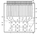
図4に示すように、第1透明基板21は、サブ開口200により構成される表示エリア51と、表示エリア51を囲むように設けられた額縁エリア59と、駆動IC54およびFPC(Flexible Printed Circuit)56などが実装される実装エリア60とで構成されている。
As shown in FIG. 4, the first
表示エリア51では、サブ開口200に対応して第1透明電極24が配置されている。第1透明電極24は、例えば、ITO(Indium Tin Oxide)などによって形成される。
In the
額縁エリア59では、複数の引き回し配線53、変換部52、および対向基板接続電極55が形成されている。ここで、変換部52について説明する。図4では詳細に図示していないが、例えば特許文献1の図12,13に示すように、第1透明基板21では各第1透明電極24から配線が引き出されており、所定のブロックごとに8本周期で短絡されている。この短絡箇所が変換部52に相当する。従って、1本の引き回し配線53から第1透明電極24へは、変換部52を介して8本周期で同じ駆動電圧が入力されることになる。
In the
実装エリア60では、駆動IC出力端子57、駆動IC入力端子58、およびFPC端子61が形成されている。駆動IC出力端子57は、引き回し配線53および変換部52を介して第1透明電極24に接続されている。駆動IC入力端子58は、入力配線62を介してFPC端子61に接続されている。対向基板接続電極55は、入力配線62を介してFPC端子61に接続されている。
In the mounting
引き回し配線53および入力配線62は、例えば、クロム(Cr)、アルミニウム(Al)、タンタル(Ta)、チタン(Ti)、モリブデン(Mo)、タングステン(W)、ニッケル(Ni)、銅(Cu)、金(Au)、銀(Ag)などの高融点金属、低抵抗金属、当該高融点金属または低抵抗金属を主成分とする合金膜、または高融点金属、低抵抗金属、および合金膜の任意の組み合わせからなる積層膜によって形成される。
The
図4に示す前提技術による第1透明基板21では、例えば、駆動IC出力端子57、駆動IC入力端子58、およびFPC端子61のうちのいずれかに静電気が入力されると、引き回し配線53または入力配線62が断線することがある。このことは、表示装置1を製造上の歩留りが低下する要因となる。
In the first
本発明の実施の形態は、上記の問題を解決するためになされたものであり、以下に詳細に説明する。 The embodiment of the present invention has been made to solve the above-described problem, and will be described in detail below.
<実施の形態1>
図5は、本発明の実施の形態1による第1透明基板21の構成の一例を示す平面図である。
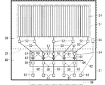
<
FIG. 5 is a plan view showing an example of the configuration of the first
図5に示すように、接続配線63は、各駆動IC出力端子57から第1透明基板21外へ延在するように形成されている。ショートリング64は、第1透明基板21外に形成されている。本実施の形態1では、各駆動IC出力端子57が、接続配線63を介してショートリング64に接続されていることを特徴としている。その他の構成は、前提技術と同様であるため、ここでは詳細な説明を省略する。
As shown in FIG. 5, the
図5は、表示装置1の製造過程、具体的には視差バリアシャッタパネル20の製造過程を示している。視差バリアシャッタパネル20の製造過程において、第1透明基板21は、例えば図6に示すようなTFTアレイ基板100に複数形成される。なお、図6の例では、ショートリング64は複数の第1透明基板21で共通して形成されているが、図5の例では、ショートリング64は各第1透明基板21に対応して別個に形成されている。図6に示すように、ショートリング64は、第1透明基板21外のTFTアレイ基板100上に形成されている。
FIG. 5 shows a manufacturing process of the
TFTアレイ基板100から第1透明基板21を切断して切り出す際、接続配線63も切断される。これにより、その後、駆動IC54およびFPC56を実装する際、各駆動IC出力端子57は電気的に独立しているため、駆動IC54の動作時にショートリング64の影響を受けることはない。
When the first
なお、図6に示すように、ショートリング64は、第1透明基板21外のTFTアレイ基板100上において、複数の第1透明基板21で共通するように形成してもよい。
As shown in FIG. 6, the
図7に示すように、各FPC端子61とショートリング64とを、接続配線63を介して接続してもよい。
As shown in FIG. 7, each
図8に示すように、各駆動IC出力端子57および各FPC端子61とショートリング64とを、接続配線63を介して接続してもよい。
As shown in FIG. 8, each drive
図9に示すように、各第1透明電極24とショートリング64とを、接続配線63を介して接続してもよい。
As shown in FIG. 9, each first
以上のことから、本実施の形態1によれば、視差バリアシャッタパネル20の製造過程において、各駆動IC出力端子57、各FPC端子61、および各第1透明電極24のうちの少なくとも1つは、接続配線63を介してショートリング64に接続されている。従って、各駆動IC出力端子57、各駆動IC入力端子58、および各FPC端子61のうちのいずれかに静電気が入力されたとしてもショートリング64を介して放電されるため、引き回し配線53または入力配線62の断線を防ぐことができる。これにより、表示装置1の製造上の歩留りを向上させることができる。
From the above, according to the first embodiment, in the manufacturing process of the parallax
<実施の形態2>
図10は、本発明の実施の形態2による第1透明基板21の構成の一例を示す平面図である。
<
FIG. 10 is a plan view showing an example of the configuration of the first
図10に示すように、ショートリング64は、第1透明基板21内に形成されている。本実施の形態2では、各駆動IC出力端子57とショートリング64との間に高抵抗素子65を設けることを特徴としている。すなわち、各駆動IC出力端子57は、接続配線63および高抵抗素子65を介してショートリング64に接続されている。その他の構成は、前提技術と同様であるため、ここでは詳細な説明を省略する。
As shown in FIG. 10, the
高抵抗素子65は、例えば、アモルファスシリコンまたはITOなど、高抵抗材料の微細パターンにより形成することができる。
The
以上のことから、本実施の形態2によれば、各駆動IC出力端子57とショートリング64との間に高抵抗素子65を設けている。従って、各駆動IC出力端子57は駆動時に影響を及ぼさないレベルで接続されるとともに、静電気対策としても機能する。これにより、表示装置1の製造上の歩留りを向上させることができる。
From the above, according to the second embodiment, the
なお、高抵抗素子65は、実施の形態1で説明した図5,7,8,9に示す構成に適用することができる。具体的には、図5において、各駆動IC出力端子57とショートリング64との間に高抵抗素子65を設けてもよい。図7において、各FPC端子61とショートリング64との間に高抵抗素子65を設けてもよい。図8において、各駆動IC出力端子57および各FPC端子61とショートリング64との間に高抵抗素子65を設けてもよい。図9において、各第1透明電極24とショートリング64との間に高抵抗素子65を設けてもよい。これらの構成の場合であっても、表示装置1の製造上の歩留りを向上させることができる。
The
また、高抵抗素子65を、各駆動IC出力端子57間、各変換部52間、各引き出し配線53間、または各第1透明電極24間などにさらに設ける構成とすれば、より効果的である。
Further, it is more effective if the
<実施の形態3>
図11は、本発明の実施の形態3による第1透明基板21の構成の一例を示す平面図である。
<
FIG. 11 is a plan view showing an example of the configuration of the first
図11に示すように、ショートリング64は、第1透明基板21内に形成されている。本実施の形態3では、各駆動IC出力端子57とショートリング64との間にスパークギャップ66を設けることを特徴としている。すなわち、各駆動IC出力端子57は、接続配線63およびスパークギャップ66を介してショートリング64に接続されている。その他の構成は、前提技術と同様であるため、ここでは詳細な説明を省略する。
As shown in FIG. 11, the
図12に示すように、スパークギャップ66は、接続配線63とショートリング64との間に設けられた間隙である。
As shown in FIG. 12, the
以上のことから、本実施の形態3によれば、各駆動IC出力端子57とショートリング64との間にスパークギャップ66を設けている。従って、各駆動IC出力端子57に静電気が入力されたとしてもスパークギャップ66およびショートリング64を介して放電されるため、引き回し配線53または入力配線62の断線を防ぐことができる。これにより、表示装置1の製造上の歩留りを向上させることができる。
From the above, according to the third embodiment, the
なお、スパークギャップ66は、実施の形態1で説明した図5,7,8,9に示す構成に適用することができる。具体的には、図5において、各駆動IC出力端子57とショートリング64との間にスパークギャップ66を設けてもよい。図7において、各FPC端子61とショートリング64との間にスパークギャップ66を設けてもよい。図8において、各駆動IC出力端子57および各FPC端子61とショートリング64との間にスパークギャップ66を設けてもよい。図9において、各第1透明電極24とショートリング64との間にスパークギャップ66を設けてもよい。これらの構成の場合であっても、表示装置1の製造上の歩留りを向上させることができる。
The
また、スパークギャップ66を、各駆動IC出力端子57間、各変換部52間、各引き出し配線53間、または各第1透明電極24間などにさらに設ける構成とすれば、より効果的である。
In addition, it is more effective if the
<実施の形態4>
図13は、本発明の実施の形態4による第1透明基板21の構成の一例を示す平面図である。
<
FIG. 13 is a plan view showing an example of the configuration of the first
図13に示すように、ショートリング64は、第1透明基板21内に形成されている。本実施の形態4では、各駆動IC出力端子57とショートリング64との間に容量67を設けることを特徴としている。すなわち、各駆動IC出力端子57は、接続配線63および容量67を介してショートリング64に接続されている。その他の構成は、前提技術と同様であるため、ここでは詳細な説明を省略する。
As shown in FIG. 13, the
容量67は、例えば、接続配線63とショートリング64とを絶縁膜を介して重畳することによって形成することができる。
The
以上のことから、本実施の形態4によれば、各駆動IC出力端子57とショートリング64との間に容量67を設けている。容量64を介して各駆動IC出力端子57とショートリング64とを容量結合させることによって、剥離帯電などによる電位差が各駆動IC出力端子57間で生じにくくなる。これにより、表示装置1の製造上の歩留りを向上させることができる。
From the above, according to the fourth embodiment, the
なお、容量67は、実施の形態1で説明した図5,7,8,9に示す構成に適用することができる。具体的には、図5において、各駆動IC出力端子57とショートリング64との間に容量67を設けてもよい。図7において、各FPC端子61とショートリング64との間に容量67を設けてもよい。図8において、各駆動IC出力端子57および各FPC端子61とショートリング64との間に容量67を設けてもよい。図9において、各第1透明電極24とショートリング64との間に容量67を設けてもよい。これらの構成の場合であっても、表示装置1の製造上の歩留りを向上させることができる。
Note that the
また、容量67を、各駆動IC出力端子57間、各変換部52間、各引き出し配線53間、または各第1透明電極24間などにさらに設ける構成とすれば、より効果的である。
Further, it is more effective if the
<実施の形態5>
図14は、本発明の実施の形態5による第1透明基板21の構成の一例を示す断面図である。
<
FIG. 14 is a cross-sectional view showing an example of the configuration of the first
図14に示すように、第1透明基板21上であっての液晶層23側には、電界シールド電極である電界シールド用透明電極84が設けられている。電界シールド用透明電極84上には第1絶縁層81が設けられている。第1絶縁層81上には、下層透明電極24aおよび第1金属層87が設けられている。第1金属層87上には駆動IC出力端子57が積層して設けられている。下層透明電極24a、第1金属層87、および駆動IC出力端子57を覆うように第2絶縁層82が設けられている。第2絶縁層82上には上層透明電極24bが設けられている。上層透明電極24bを覆うように第3絶縁層83が設けられている。駆動IC出力端子57の一部は、第2絶縁層82および第3絶縁層83から露出している。
As shown in FIG. 14, an electric field shielding
本実施の形態5では、第1透明基板21上に電界シールド用透明電極84を設けることを特徴としている。その他の構成は、前提技術と同様であるため、ここでは詳細な説明を省略する。
The fifth embodiment is characterized in that a
電界シールド用透明電極84は、例えば、ITOなどによって形成することができる。図14において、電界シールド用透明電極84は、第1透明基板21上の全面に形成されているが、これに限るものではない。例えば、電界シールド用透明電極84は、端面において露出しないようにパターニングされてもよい。あるいは、図示しないが、FPC端子61または駆動IC出力端子57から延びる配線を電界シールド用透明電極84と電気的に接続して、電界シールド用透明電極84に電位が印加されるようにしてもよい。さらに、例えば表示装置の筐体やフレームのように一定電位に維持される箇所(図示しない)と電界シールド用透明電極84とを電気的に接続してもよい。これにより、電界シールド用透明電極84はフローティングではなくなるため、シールド効果を増大させることが可能となる。
The electric field shielding
以上のことから、本実施の形態5によれば、第1透明基板21上に電界シールド用透明電極84を設けているため、剥離帯電などによる電位差が各駆動IC出力端子57間で生じにくくなる。これにより、表示装置1の製造上の歩留りを向上させることができる。
From the above, according to the fifth embodiment, since the electric field shielding
<実施の形態6>
図15は、本発明の実施の形態6による視差バリアシャッタパネル20の構成の一例を示す断面図である。なお、図15は、表示装置1の製造過程、具体的には視差バリアシャッタパネル20の製造過程を示している。
<
FIG. 15 is a cross-sectional view showing an example of the configuration of the parallax
図15に示すように、第1透明基板21上であっての液晶層23側には、下層透明電極24aおよび第1金属層87が設けられている。第1金属層87上には駆動IC出力端子57が積層して設けられている。下層透明電極24a、第1金属層87、および駆動IC出力端子57を覆うように第1絶縁層81が設けられている。第1絶縁層81上には上層透明電極24bが設けられている。上層透明電極24bを覆うように第2絶縁層82が設けられている。駆動IC出力端子57の一部は、第1絶縁層81および第2絶縁層82から露出している。第2透明基板22上であって液晶層23側には、第2透明電極25が設けられている。
As shown in FIG. 15, the lower
第2絶縁層82と第2透明電極25との間には、液晶層23がシール85によって封止されている。駆動IC出力端子57と第2透明電極25とは、接続用ダミーシール86を介して電気的に接続されている。なお、図15では、1つの駆動IC出力端子57と第2透明電極25とが接続用ダミーシール86を介して電気的に接続されているが、他の駆動IC出力端子57もそれぞれ第2透明電極25と接続用ダミーシール86を介して電気的に接続されている。TFTアレイ基板100から第1透明基板21を切断して切り出す際、接続用ダミーシール86も切断される。
The
本実施の形態6では、駆動IC出力端子57と第2透明電極25とを接続用ダミーシール86を介して電気的に接続することを特徴としている。その他の構成は、前提技術と同様であるため、ここでは詳細な説明を省略する。
The sixth embodiment is characterized in that the drive
接続用ダミーシール86は、シール85に導電性の粒子などを混入することによって形成することができる。導電性の粒子としては、例えば金パールなどが挙げられる。
The
以上のことから、本実施の形態6によれば、TFTアレイ基板100から第1透明基板21を切断して切り出すまでは、各駆動IC出力端子57と第2透明電極25とは接続用ダミーシール86を介して電気的に接続されているため、第2透明電極25を実施の形態1〜4で説明したショートリング64と同様に扱うことができる。すなわち、表示装置1の製造上の歩留りを向上させることができる。
From the above, according to the sixth embodiment, each drive
なお、図15では、各駆動IC出力端子57と第2透明電極25とを接続用ダミーシール86を介して電気的に接続する場合について説明したが、これに限るものではない。例えば、各駆動IC入力端子58と第2透明電極25とを接続用ダミーシール86を介して電気的に接続してもよく、各FPC端子61と第2透明電極25とを接続用ダミーシール86を介して電気的に接続してもよい。
In addition, although FIG. 15 demonstrated the case where each drive
<実施の形態7>
図16は、本発明の実施の形態7による第1透明基板21の構成の一例を示す平面図である。
<
FIG. 16 is a plan view showing an example of the configuration of the first
図16に示すように、ショートリング64は、第1透明基板21内に形成されている。本実施の形態7では、各駆動IC出力端子57とショートリング64との間に非線形素子68を設けることを特徴としている。すなわち、各駆動IC出力端子57は、接続配線63および非線形素子68を介してショートリング64に接続されている。その他の構成は、前提技術と同様であるため、ここでは詳細な説明を省略する。
As shown in FIG. 16, the
非線形素子68は、例えば図17に示すように、アモルファスシリコンまたは酸化物半導体などを用いて形成した第1トランジスタ70および第2トランジスタ71を双方向に接続することによって形成することができる。
For example, as shown in FIG. 17, the
非線形素子68に酸化物半導体を用いた場合は、第1透明電極24を導体化して伝導体とし、非線形素子68を半導体として用いることによって、視差バリアシャッタパネル20の生産性が改善される。第1透明電極24を導体化する方法としては、酸化物半導体を成膜した後に、表示エリア51のみを露出させた状態で水素プラズマ処理を行う方法などがある。非線形素子68に酸化物半導体を用いた場合における表示エリア51と非線形素子68を構成する第1トランジスタ70との断面図を図18に示す。例えば、図18において、第1絶縁層81上に酸化物半導体を成膜し、表示エリア51を露出させた状態で水素プラズマ処理を行う。その後、フォトリソグラフィ工程およびエッチング工程などを行うことによって所望のパターンに加工し、上層透明電極24bと半導体層89とを同時に形成することができる。
In the case where an oxide semiconductor is used for the
以上のことから、本実施の形態7によれば、各駆動IC出力端子57とショートリング64との間に非線形素子68を設けている。従って、各駆動IC出力端子57に静電気が入力されたとしても非線形素子68およびショートリング64を介して放電されるため、引き回し配線53または入力配線62の断線を防ぐことができる。これにより、表示装置1の製造上の歩留りを向上させることができる。
From the above, according to the seventh embodiment, the
なお、非線形素子68は、実施の形態1で説明した図5,7,8,9に示す構成に適用することができる。具体的には、図5において、各駆動IC出力端子57とショートリング64との間に非線形素子68を設けてもよい。図7において、各FPC端子61とショートリング64との間に非線形素子68を設けてもよい。図8において、各駆動IC出力端子57および各FPC端子61とショートリング64との間に非線形素子68を設けてもよい。図9において、各第1透明電極24とショートリング64との間に非線形素子68を設けてもよい。これらの構成の場合であっても、表示装置1の製造上の歩留りを向上させることができる。
The
また、非線形素子68を、各駆動IC出力端子57間、各変換部52間、各引き出し配線53間、または各第1透明電極24間などにさらに設ける構成とすれば、より効果的である。
Further, it is more effective if the
<実施の形態8>
実施の形態2〜7では、視差バリアシャッタパネル20において、ショートリング64と、高抵抗素子65、スパークギャップ66、容量67、または非線形素子68のようなサージ電圧緩衝部とを設け、各第1透明電極24がサージ電圧緩衝部およびショートリング64を介して互いに接続される形態について説明した。本実施の形態8では、ショートリング64を省略し、隣接する各第1透明電極24間にサージ電圧緩衝部を設けることを特徴とする。
<Eighth embodiment>
In the second to seventh embodiments, the parallax
図19は、本実施の形態8による第1透明基板21の構成の一例を示す平面図である。図19に示すように、本実施の形態8では、隣接する各駆動IC出力端子57間に高抵抗素子65を設けることを特徴としている。すなわち、隣接する各駆動IC出力端子57は、接続配線63および高抵抗素子65を介して接続されている。
FIG. 19 is a plan view showing an example of the configuration of the first
実施の形態2〜7では、各第1透明電極24における電荷は、ショートリング64を介して放電されていた。一方、本実施の形態8では、ショートリングを介した放電はないが、高抵抗素子65を介して接続された隣接する各第1透明電極24と電荷を分け合うことになり、静電気によるダメージを軽減する効果がある。
In the second to seventh embodiments, the charge in each first
本実施の形態8は、ショートリングを備える形態よりも静電気に対する耐久性は劣るものの、パターン設計上などの理由からショートリングを設けることができない場合には本実施の形態8を採用することに意義がある。 Although the eighth embodiment is less durable against static electricity than the configuration provided with the short ring, it is meaningful to adopt the eighth embodiment when the short ring cannot be provided for reasons such as pattern design. There is.
なお、図19では、隣接する各駆動IC出力端子57間に高抵抗素子65を設ける形態について説明したが、高抵抗素子65に代えて、スパークギャップ66、容量67、または非線形素子68のいずれか1つが設けられる形態であっても、上記と同様の効果を奏する。
In FIG. 19, the form in which the
<変形例1>
図20は、本実施の形態8の変形例1であり、第1透明基板21の構成の一例を示す平面図である。図20に示すように、本変形例1では、隣接する各FPC端子61間に高抵抗素子65を設けることを特徴としている。すなわち、隣接する各FPC端子61は、接続配線63および高抵抗素子65を介して接続されている。
<
FIG. 20 is a plan view showing an example of the configuration of the first
本変形例1は、ショートリングを設けない点は実施の形態8と共通するが、高抵抗素子65を設ける箇所が異なる。本変形例1では、各第1透明電極24における電荷の放電よりは、各FPC端子61から駆動IC入力端子58への電荷流入によって駆動IC54が受けるダメージを抑制する効果が高い。
The first modification is common to the eighth embodiment in that the short ring is not provided, but the place where the
なお、図20では、隣接する各FPC端子61間に高抵抗素子65を設ける形態について説明したが、高抵抗素子65に代えて、スパークギャップ66、容量67、または非線形素子68のいずれか1つが設けられる形態であっても、上記と同様の効果を奏する。
In FIG. 20, the
<変形例2>
図21は、実施の形態8の変形例2であり、第1透明基板21の構成の一例を示す平面図である。図21に示すように、本変形例2では、隣接する各第1透明電極24間に高抵抗素子65を設けることを特徴としている。すなわち、隣接する各第1透明電極21は、接続配線63および高抵抗素子65を介して接続されている。
<
FIG. 21 is a plan view showing an example of the configuration of the first
本変形例2は、ショートリングを設けない点は実施の形態8と共通するが、高抵抗素子65を設ける箇所が異なる。本変形例2では、各第1透明電極21の変換部52が設けられていない側、すなわち表示エリア51を介して変換部52と対向する側に高抵抗素子65を設けている。本変形例2でも、実施の形態8と同様の効果を奏する。また、通常、変換部52を設ける領域には隙間がないため高抵抗素子65を設けることは困難であるが、本変形例2ではそのような制限がなく、高抵抗素子65を設けることができる。
The second modification is common to the eighth embodiment in that the short ring is not provided, but the place where the
なお、図21では、隣接する各第1透明電極24間に高抵抗素子65を設ける形態について説明したが、高抵抗素子65に代えて、スパークギャップ66、容量67、または非線形素子68のいずれか1つが設けられる形態であっても、上記と同様の効果を奏する。
In FIG. 21, the
なお、本発明は、その発明の範囲内において、各実施の形態を自由に組み合わせたり、各実施の形態を適宜、変形、省略することが可能である。 It should be noted that the present invention can be freely combined with each other within the scope of the invention, and each embodiment can be appropriately modified or omitted.
1 表示装置、10 表示パネル、11 透明基板、12 透明基板、13 液晶層、14 サブ画素透明電極、15 対向透明電極、16 中間偏光板、17 裏面偏光板、18 遮光壁、20 視差バリアシャッタパネル、21 第1透明基板、22 第2透明基板、23 液晶層、24 第1透明電極、25 第2透明電極、26 表示面偏光板、30 バックライト、31 検出部、32 制御部、40a 右眼用サブ画素、40b 左眼用サブ画素、41 サブ画素ペア、51 表示エリア、52 変換部、53 引き回し配線、54 駆動IC、55 対向基板接続電極、56 FPC、57 駆動IC出力端子、58 駆動IC入力端子、59 額縁エリア、60 実装エリア、61 FPC端子、62 入力配線、63 接続配線、64 ショートリング、65 高抵抗素子、66 スパークギャップ、67 容量、68 非線形素子、70 第1トランジスタ、71 第2トランジスタ、81 第1絶縁層、82 第2絶縁層、83 第3絶縁層、84 電界シールド用透明電極、85 シール、86 接続用ダミーシール、87 第1金属層、88 第2金属層、89 半導体層、100 TFTアレイ基板、200 サブ開口、300 総合開口。 DESCRIPTION OF SYMBOLS 1 Display apparatus, 10 Display panel, 11 Transparent substrate, 12 Transparent substrate, 13 Liquid crystal layer, 14 Sub pixel transparent electrode, 15 Opposing transparent electrode, 16 Intermediate polarizing plate, 17 Back polarizing plate, 18 Light shielding wall, 20 Parallax barrier shutter panel , 21 1st transparent substrate, 22 2nd transparent substrate, 23 Liquid crystal layer, 24 1st transparent electrode, 25 2nd transparent electrode, 26 Display surface polarizing plate, 30 Backlight, 31 Detection unit, 32 Control unit, 40a Right eye Sub-pixel, 40b sub-pixel for left eye, 41 sub-pixel pair, 51 display area, 52 conversion section, 53 lead-out wiring, 54 drive IC, 55 counter substrate connection electrode, 56 FPC, 57 drive IC output terminal, 58 drive IC Input terminal, 59 Frame area, 60 Mounting area, 61 FPC terminal, 62 Input wiring, 63 Connection wiring, 64 Short circuit 65, high resistance element, 66 spark gap, 67 capacitance, 68 nonlinear element, 70 first transistor, 71 second transistor, 81 first insulating layer, 82 second insulating layer, 83 third insulating layer, 84 for electric field shielding Transparent electrode, 85 seal, 86 dummy seal for connection, 87 first metal layer, 88 second metal layer, 89 semiconductor layer, 100 TFT array substrate, 200 sub-opening, 300 general opening.
Claims (24)
前記表示パネルと対向して設けられた視差バリアシャッタパネルと、
を備え、
前記視差バリアシャッタパネルは、
一定間隔で設けられた複数の透明電極と、
各前記透明電極に印加する電圧を制御する駆動ICと、
前記駆動ICの入力端子と電気的に接続されたFPC端子を有するFPCと、
を有し、
各前記透明電極、前記駆動ICの出力端子、および前記FPC端子のうちの少なくとも1つは、ショートリングと電気的に接続されていることを特徴とする、表示装置。 A display panel;
A parallax barrier shutter panel provided facing the display panel;
With
The parallax barrier shutter panel is:
A plurality of transparent electrodes provided at regular intervals;
A driving IC for controlling a voltage applied to each of the transparent electrodes;
An FPC having an FPC terminal electrically connected to an input terminal of the driving IC;
Have
At least one of each of the transparent electrodes, the output terminal of the driving IC, and the FPC terminal is electrically connected to a short ring.
前記FPCは、各前記入力端子と電気的に接続された複数の前記FPC端子を有し、
前記高抵抗素子は、各前記出力端子間、および各前記FPC端子間のうちの少なくとも1つに設けられていることを特徴とする、請求項2に記載の表示装置。 The drive IC has a plurality of output terminals electrically connected to the plurality of transparent electrodes, and a plurality of the input terminals,
The FPC has a plurality of the FPC terminals electrically connected to the input terminals,
The display device according to claim 2, wherein the high resistance element is provided between at least one of the output terminals and between the FPC terminals.
前記FPCは、各前記入力端子と電気的に接続された複数の前記FPC端子を有し、
前記スパークギャップは、各前記出力端子間、および各前記FPC端子間のうちの少なくとも1つに設けられていることを特徴とする、請求項5に記載の表示装置。 The drive IC has a plurality of output terminals electrically connected to the plurality of transparent electrodes, and a plurality of the input terminals,
The FPC has a plurality of the FPC terminals electrically connected to the input terminals,
The display device according to claim 5, wherein the spark gap is provided between at least one of the output terminals and between the FPC terminals.
前記FPCは、各前記入力端子と電気的に接続された複数の前記FPC端子を有し、
前記容量は、各前記出力端子間、および各前記FPC端子間のうちの少なくとも1つに設けられていることを特徴とする、請求項8に記載の表示装置。 The drive IC has a plurality of output terminals electrically connected to the plurality of transparent electrodes, and a plurality of the input terminals,
The FPC has a plurality of the FPC terminals electrically connected to the input terminals,
The display device according to claim 8, wherein the capacitor is provided between at least one of the output terminals and between the FPC terminals.
前記FPCは、各前記入力端子と電気的に接続された複数の前記FPC端子を有し、
前記非線形素子は、各前記出力端子間、および各前記FPC端子間のうちの少なくとも1つに設けられていることを特徴とする、請求項11に記載の表示装置。 The drive IC has a plurality of output terminals electrically connected to the plurality of transparent electrodes, and a plurality of the input terminals,
The FPC has a plurality of the FPC terminals electrically connected to the input terminals,
The display device according to claim 11, wherein the nonlinear element is provided between at least one of the output terminals and between the FPC terminals.
前記ショートリングは、前記基板上であって前記視差バリアシャッタパネル外において、各前記視差バリアシャッタパネルで共通して設けられていることを特徴とする、請求項1から13のいずれか1項に記載の表示装置。 A plurality of the parallax barrier shutter panels are provided on one substrate,
The said short ring is provided in common with each said parallax barrier shutter panel on the said board | substrate and the said parallax barrier shutter panel, The any one of Claim 1 to 13 characterized by the above-mentioned. The display device described.
前記表示パネルと対向して設けられた視差バリアシャッタパネルと、
を備え、
前記視差バリアシャッタパネルは、
透明基板と、
前記透明基板上に設けられた電界シールド電極と、
前記電界シールド電極を覆うように設けられた絶縁層と、
前記絶縁層上に一定間隔で設けられた複数の透明電極と、
を有することを特徴とする、表示装置。 A display panel;
A parallax barrier shutter panel provided facing the display panel;
With
The parallax barrier shutter panel is:
A transparent substrate;
An electric field shield electrode provided on the transparent substrate;
An insulating layer provided to cover the electric field shield electrode;
A plurality of transparent electrodes provided at regular intervals on the insulating layer;
A display device comprising:
前記表示パネルと対向して設けられた視差バリアシャッタパネルと、
を備え、
前記視差バリアシャッタパネルは、
一定間隔で設けられた複数の透明電極と、
各前記透明電極に印加する電圧を制御する駆動ICと、
前記駆動ICの入力端子と電気的に接続されたFPC端子を有するFPCと、
とを有し、
前記駆動ICは、前記複数の透明電極と電気的に接続された複数の出力端子と、複数の前記入力端子とを有し、
前記FPCは、各前記入力端子と電気的に接続された複数の前記FPC端子を有し、
前記視差バリアシャッタパネルは、各前記透明電極間、各出力端子間、または各前記FPC端子間に高抵抗素子をさらに備えることを特徴とする、表示装置。 A display panel;
A parallax barrier shutter panel provided facing the display panel;
With
The parallax barrier shutter panel is:
A plurality of transparent electrodes provided at regular intervals;
A driving IC for controlling a voltage applied to each of the transparent electrodes;
An FPC having an FPC terminal electrically connected to an input terminal of the driving IC;
And
The drive IC has a plurality of output terminals electrically connected to the plurality of transparent electrodes, and a plurality of the input terminals,
The FPC has a plurality of the FPC terminals electrically connected to the input terminals,
The display device according to claim 1, wherein the parallax barrier shutter panel further includes a high resistance element between the transparent electrodes, between the output terminals, or between the FPC terminals.
前記高抵抗素子は、各前記透明電極を介して前記変換部と対向する側において、各前記透明電極間に設けられていることを特徴とする、請求項17に記載の表示装置。 The parallax barrier shutter panel further includes a conversion unit between each transparent electrode and each output terminal,
The display device according to claim 17, wherein the high resistance element is provided between the transparent electrodes on a side facing the conversion unit via the transparent electrodes.
(b)前記表示パネルと対向して視差バリアシャッタパネルを設ける工程と、
を備え、
前記工程(b)は、
(c)透明基板上に、複数の透明電極を一定間隔で形成する工程と、
(d)前記透明基板上に、各前記透明電極に印加する電圧を制御する駆動ICの入力端子および出力端子を形成する工程と、
(e)前記透明基板上に、前記駆動ICの入力端子と電気的に接続されたFPC端子を形成する工程と、
(f)各前記透明電極、前記駆動ICの出力端子、および前記FPC端子のうちの少なくとも1つと、前記視差バリアシャッタパネル外の前記透明基板上に形成されたショートリングとを電気的に接続する工程と、
(g)前記工程(f)で行った前記接続を切断し、前記透明基板から前記視差バリアシャッタパネルを切り出す工程と、
を含むことを特徴とする、表示装置の製造方法。 (A) preparing a display panel;
(B) providing a parallax barrier shutter panel facing the display panel;
With
The step (b)
(C) forming a plurality of transparent electrodes at regular intervals on the transparent substrate;
(D) forming an input terminal and an output terminal of a driving IC for controlling a voltage applied to each of the transparent electrodes on the transparent substrate;
(E) forming an FPC terminal electrically connected to the input terminal of the drive IC on the transparent substrate;
(F) electrically connecting at least one of each transparent electrode, the output terminal of the drive IC, and the FPC terminal to a short ring formed on the transparent substrate outside the parallax barrier shutter panel. Process,
(G) cutting the connection made in the step (f) and cutting the parallax barrier shutter panel from the transparent substrate;
A method for manufacturing a display device, comprising:
(h)各前記透明電極、前記駆動ICの出力端子、および前記FPC端子のうちの少なくとも1つと前記ショートリングとの間に非線形素子を形成する工程
をさらに備えることを特徴とする、請求項20に記載の表示装置の製造方法。 The step (b)
21. The method of claim 20, further comprising: forming a non-linear element between at least one of each of the transparent electrodes, the output terminal of the driving IC, and the FPC terminal and the short ring. The manufacturing method of the display apparatus as described in 1 ..
(i)前記透明基板上に電界シールド電極を形成する工程と、
(j)前記電界シールド電極を覆うように絶縁層を形成する工程と、
をさらに備え、
前記工程(c)において、前記複数の透明電極は前記絶縁層上に形成され、
前記工程(d)において、前記入力端子および前記出力端子は前記絶縁層上に形成され、
前記電界シールド電極は、前記FPC端子または前記出力端子と電気的に接続されていることを特徴とする、請求項20に記載の表示装置の製造方法。 In the step (b), before the step (c),
(I) forming an electric field shield electrode on the transparent substrate;
(J) forming an insulating layer so as to cover the electric field shield electrode;
Further comprising
In the step (c), the plurality of transparent electrodes are formed on the insulating layer,
In the step (d), the input terminal and the output terminal are formed on the insulating layer,
21. The method of manufacturing a display device according to claim 20, wherein the electric field shield electrode is electrically connected to the FPC terminal or the output terminal.
(b)前記表示パネルと対向して視差バリアシャッタパネルを設ける工程と、
を備え、
前記工程(b)は、
(c)第1透明基板上に、複数の透明電極を一定間隔で形成する工程と、
(d)前記第1透明基板上に、各前記透明電極に印加する電圧を制御する駆動ICの入力端子および出力端子を形成する工程と、
(e)前記第1透明基板上に、前記駆動ICの入力端子と電気的に接続されたFPC端子を形成する工程と、
(f)前記第1透明基板と対向する第2透明基板上に第2透明電極を形成する工程と、
(g)前記駆動ICの入力端子、前記駆動ICの出力端子、および前記FPC端子のうちの少なくとも1つと、前記第2透明電極とを電気的に接続する工程と、
(h)前記工程(g)で行った前記接続を切断し、前記第1透明基板および前記第2透明基板から前記視差バリアシャッタパネルを切り出す工程と、
を含むことを特徴とする、表示装置の製造方法。 (A) preparing a display panel;
(B) providing a parallax barrier shutter panel facing the display panel;
With
The step (b)
(C) forming a plurality of transparent electrodes at regular intervals on the first transparent substrate;
(D) forming an input terminal and an output terminal of a driving IC for controlling a voltage applied to each of the transparent electrodes on the first transparent substrate;
(E) forming an FPC terminal electrically connected to the input terminal of the driving IC on the first transparent substrate;
(F) forming a second transparent electrode on a second transparent substrate facing the first transparent substrate;
(G) electrically connecting at least one of the input terminal of the drive IC, the output terminal of the drive IC, and the FPC terminal to the second transparent electrode;
(H) cutting the connection made in the step (g) and cutting the parallax barrier shutter panel from the first transparent substrate and the second transparent substrate;
A method for manufacturing a display device, comprising:
Priority Applications (3)
| Application Number | Priority Date | Filing Date | Title |
|---|---|---|---|
| JP2018079966A JP2019191214A (en) | 2018-04-18 | 2018-04-18 | Display device and method for manufacturing the same |
| US16/371,151 US20190324333A1 (en) | 2018-04-18 | 2019-04-01 | Display device and method of manufacturing display device |
| CN201910294409.1A CN110389452A (en) | 2018-04-18 | 2019-04-12 | Display device and its manufacturing method |
Applications Claiming Priority (1)
| Application Number | Priority Date | Filing Date | Title |
|---|---|---|---|
| JP2018079966A JP2019191214A (en) | 2018-04-18 | 2018-04-18 | Display device and method for manufacturing the same |
Publications (2)
| Publication Number | Publication Date |
|---|---|
| JP2019191214A true JP2019191214A (en) | 2019-10-31 |
| JP2019191214A5 JP2019191214A5 (en) | 2020-11-05 |
Family
ID=68235957
Family Applications (1)
| Application Number | Title | Priority Date | Filing Date |
|---|---|---|---|
| JP2018079966A Withdrawn JP2019191214A (en) | 2018-04-18 | 2018-04-18 | Display device and method for manufacturing the same |
Country Status (3)
| Country | Link |
|---|---|
| US (1) | US20190324333A1 (en) |
| JP (1) | JP2019191214A (en) |
| CN (1) | CN110389452A (en) |
Families Citing this family (2)
| Publication number | Priority date | Publication date | Assignee | Title |
|---|---|---|---|---|
| CN114005376A (en) * | 2020-07-27 | 2022-02-01 | 北京芯海视界三维科技有限公司 | Light-emitting module and display device |
| CN113514989A (en) * | 2021-06-23 | 2021-10-19 | 上海中航光电子有限公司 | Display panel and display device |
Family Cites Families (15)
| Publication number | Priority date | Publication date | Assignee | Title |
|---|---|---|---|---|
| KR101087568B1 (en) * | 2004-12-30 | 2011-11-28 | 엘지디스플레이 주식회사 | parallax barrier liquid crystal display panel for stereoscopic 3-D display apparatus and manufacturing method the same |
| EP2472497B1 (en) * | 2009-08-25 | 2014-10-01 | Sharp Kabushiki Kaisha | Display panel, display device, and method for manufacturing same |
| JP5609562B2 (en) * | 2010-11-10 | 2014-10-22 | ソニー株式会社 | Stereo imaging device |
| CN102062985B (en) * | 2010-11-16 | 2012-02-22 | 深圳超多维光电子有限公司 | Liquid crystal lens, control method thereof and 3D display device |
| WO2012144434A1 (en) * | 2011-04-22 | 2012-10-26 | シャープ株式会社 | Display device |
| TW201317669A (en) * | 2011-10-25 | 2013-05-01 | Hannstar Display Corp | Display device, parallax barrier, and driving methods for 3D display |
| US20150070607A1 (en) * | 2012-04-06 | 2015-03-12 | Sharp Kabushiki Kaisha | Stereoscopic display apparatus |
| KR101476884B1 (en) * | 2012-06-22 | 2014-12-26 | 엘지디스플레이 주식회사 | Parallax Barrier Type Stereoscopic Image Display Device |
| CN103698914B (en) * | 2013-12-19 | 2017-04-05 | 京东方科技集团股份有限公司 | Liquid crystal grating, display device and driving method |
| CN203673183U (en) * | 2014-01-28 | 2014-06-25 | 重庆卓美华视光电有限公司 | Liquid crystal lens and stereo display device using same |
| CN103852926B (en) * | 2014-03-28 | 2018-03-30 | 信利半导体有限公司 | Liquid crystal grating and preparation method thereof, display device |
| JP2016029475A (en) * | 2014-07-22 | 2016-03-03 | 株式会社ジャパンディスプレイ | Liquid crystal display device and electronic apparatus |
| CN105911707A (en) * | 2016-06-15 | 2016-08-31 | 苏州众显电子科技有限公司 | Electric drive liquid crystal stereoscopic display element, manufacturing method thereof, and display device |
| US10477192B2 (en) * | 2016-09-14 | 2019-11-12 | Semiconductor Energy Laboratory Co., Ltd. | Display system and electronic device |
| CN108828849A (en) * | 2018-06-05 | 2018-11-16 | 中山大学 | The preparation method of flexible liquid crystal lens and its resistance gradual change electrode |
-
2018
- 2018-04-18 JP JP2018079966A patent/JP2019191214A/en not_active Withdrawn
-
2019
- 2019-04-01 US US16/371,151 patent/US20190324333A1/en not_active Abandoned
- 2019-04-12 CN CN201910294409.1A patent/CN110389452A/en active Pending
Also Published As
| Publication number | Publication date |
|---|---|
| CN110389452A (en) | 2019-10-29 |
| US20190324333A1 (en) | 2019-10-24 |
Similar Documents
| Publication | Publication Date | Title |
|---|---|---|
| KR101419233B1 (en) | Liquid Crystal Lens Electrically driven and Stereoscopy Display Device Using the Same | |
| US9250447B2 (en) | Method for forming autostereoscopic image | |
| TWI629623B (en) | Display device | |
| US9874770B2 (en) | Display device | |
| KR101362157B1 (en) | Liquid Crystal Lens Electrically Driven and Display Device Using the Same | |
| JP5456177B2 (en) | Touch panel, display device including the same, and method for manufacturing touch panel | |
| EP2453291B1 (en) | Display device | |
| JP5632764B2 (en) | Stereoscopic image display device | |
| KR20090006473A (en) | Liquid crystal lens electrically driven and steroscopy display device | |
| JP6573467B2 (en) | Image display device and liquid crystal panel | |
| KR101580362B1 (en) | Parallax barrier and display device | |
| KR20130101236A (en) | Barrier substrate, barrier panel having the same and display apparatus having the same | |
| US20190158816A1 (en) | Image display device | |
| JP2019191214A (en) | Display device and method for manufacturing the same | |
| JP6983547B2 (en) | Image display device | |
| KR101859483B1 (en) | Stereoscopic display device and method for manufacturing the same | |
| US20130265510A1 (en) | Three-dimensional display device and active optical element thereof | |
| WO2021220954A1 (en) | Electro-optical panel, barrier shutter panel, display device, and display panel | |
| JP6046795B2 (en) | Manufacturing method of liquid crystal lens | |
| US20220210394A1 (en) | Switchable barrier and 3d display device having thereof | |
| JP2020134917A (en) | Image display device, and method for manufacturing parallax barrier shutter panel used in image display device |
Legal Events
| Date | Code | Title | Description |
|---|---|---|---|
| A521 | Request for written amendment filed |
Free format text: JAPANESE INTERMEDIATE CODE: A523 Effective date: 20200916 |
|
| A621 | Written request for application examination |
Free format text: JAPANESE INTERMEDIATE CODE: A621 Effective date: 20200916 |
|
| A977 | Report on retrieval |
Free format text: JAPANESE INTERMEDIATE CODE: A971007 Effective date: 20210819 |
|
| A761 | Written withdrawal of application |
Free format text: JAPANESE INTERMEDIATE CODE: A761 Effective date: 20210929 |