JP2019149472A - Semiconductor device and dicing method - Google Patents
Semiconductor device and dicing method Download PDFInfo
- Publication number
- JP2019149472A JP2019149472A JP2018033567A JP2018033567A JP2019149472A JP 2019149472 A JP2019149472 A JP 2019149472A JP 2018033567 A JP2018033567 A JP 2018033567A JP 2018033567 A JP2018033567 A JP 2018033567A JP 2019149472 A JP2019149472 A JP 2019149472A
- Authority
- JP
- Japan
- Prior art keywords
- silicon substrate
- semiconductor device
- dicing
- layer
- metal layer
- Prior art date
- Legal status (The legal status is an assumption and is not a legal conclusion. Google has not performed a legal analysis and makes no representation as to the accuracy of the status listed.)
- Pending
Links
- 239000004065 semiconductor Substances 0.000 title claims abstract description 97
- 238000000034 method Methods 0.000 title claims description 24
- XUIMIQQOPSSXEZ-UHFFFAOYSA-N Silicon Chemical compound [Si] XUIMIQQOPSSXEZ-UHFFFAOYSA-N 0.000 claims abstract description 62
- 229910052710 silicon Inorganic materials 0.000 claims abstract description 62
- 239000010703 silicon Substances 0.000 claims abstract description 62
- 239000000758 substrate Substances 0.000 claims abstract description 58
- 229910052751 metal Inorganic materials 0.000 claims description 70
- 239000002184 metal Substances 0.000 claims description 70
- 238000005520 cutting process Methods 0.000 claims description 23
- PXHVJJICTQNCMI-UHFFFAOYSA-N Nickel Chemical compound [Ni] PXHVJJICTQNCMI-UHFFFAOYSA-N 0.000 claims description 6
- 239000010936 titanium Substances 0.000 claims description 6
- KDLHZDBZIXYQEI-UHFFFAOYSA-N Palladium Chemical compound [Pd] KDLHZDBZIXYQEI-UHFFFAOYSA-N 0.000 claims description 5
- 239000010931 gold Substances 0.000 claims description 4
- 229910052802 copper Inorganic materials 0.000 claims description 3
- 239000010949 copper Substances 0.000 claims description 3
- 229910052737 gold Inorganic materials 0.000 claims description 3
- 229910052759 nickel Inorganic materials 0.000 claims description 3
- 229910052698 phosphorus Inorganic materials 0.000 claims description 3
- 229910052709 silver Inorganic materials 0.000 claims description 3
- 229910052719 titanium Inorganic materials 0.000 claims description 3
- 239000011701 zinc Substances 0.000 claims description 3
- RYGMFSIKBFXOCR-UHFFFAOYSA-N Copper Chemical compound [Cu] RYGMFSIKBFXOCR-UHFFFAOYSA-N 0.000 claims description 2
- OAICVXFJPJFONN-UHFFFAOYSA-N Phosphorus Chemical compound [P] OAICVXFJPJFONN-UHFFFAOYSA-N 0.000 claims description 2
- RTAQQCXQSZGOHL-UHFFFAOYSA-N Titanium Chemical compound [Ti] RTAQQCXQSZGOHL-UHFFFAOYSA-N 0.000 claims description 2
- HCHKCACWOHOZIP-UHFFFAOYSA-N Zinc Chemical compound [Zn] HCHKCACWOHOZIP-UHFFFAOYSA-N 0.000 claims description 2
- PCHJSUWPFVWCPO-UHFFFAOYSA-N gold Chemical compound [Au] PCHJSUWPFVWCPO-UHFFFAOYSA-N 0.000 claims description 2
- 229910052763 palladium Inorganic materials 0.000 claims description 2
- 239000011574 phosphorus Substances 0.000 claims description 2
- 239000004332 silver Substances 0.000 claims description 2
- 229910052725 zinc Inorganic materials 0.000 claims description 2
- BQCADISMDOOEFD-UHFFFAOYSA-N Silver Chemical compound [Ag] BQCADISMDOOEFD-UHFFFAOYSA-N 0.000 claims 1
- 230000008569 process Effects 0.000 description 15
- 229910000679 solder Inorganic materials 0.000 description 12
- 230000004048 modification Effects 0.000 description 9
- 238000012986 modification Methods 0.000 description 9
- 238000010586 diagram Methods 0.000 description 7
- 230000015572 biosynthetic process Effects 0.000 description 6
- 239000011347 resin Substances 0.000 description 5
- 229920005989 resin Polymers 0.000 description 5
- 230000000694 effects Effects 0.000 description 4
- 238000004519 manufacturing process Methods 0.000 description 4
- 239000000126 substance Substances 0.000 description 4
- 239000007767 bonding agent Substances 0.000 description 3
- 238000005530 etching Methods 0.000 description 3
- 238000005498 polishing Methods 0.000 description 3
- 238000004544 sputter deposition Methods 0.000 description 3
- KRHYYFGTRYWZRS-UHFFFAOYSA-N Fluorane Chemical compound F KRHYYFGTRYWZRS-UHFFFAOYSA-N 0.000 description 2
- 238000005452 bending Methods 0.000 description 2
- 230000007547 defect Effects 0.000 description 2
- 229910000040 hydrogen fluoride Inorganic materials 0.000 description 2
- 230000006872 improvement Effects 0.000 description 2
- 239000000463 material Substances 0.000 description 2
- JMASRVWKEDWRBT-UHFFFAOYSA-N Gallium nitride Chemical compound [Ga]#N JMASRVWKEDWRBT-UHFFFAOYSA-N 0.000 description 1
- 230000004913 activation Effects 0.000 description 1
- 230000004888 barrier function Effects 0.000 description 1
- 230000008859 change Effects 0.000 description 1
- 238000003486 chemical etching Methods 0.000 description 1
- 238000004140 cleaning Methods 0.000 description 1
- 239000004020 conductor Substances 0.000 description 1
- 230000006866 deterioration Effects 0.000 description 1
- 229910003460 diamond Inorganic materials 0.000 description 1
- 239000010432 diamond Substances 0.000 description 1
- 238000001312 dry etching Methods 0.000 description 1
- 230000009977 dual effect Effects 0.000 description 1
- 239000000428 dust Substances 0.000 description 1
- 230000005496 eutectics Effects 0.000 description 1
- 238000005755 formation reaction Methods 0.000 description 1
- 239000007789 gas Substances 0.000 description 1
- 230000005484 gravity Effects 0.000 description 1
- 230000012447 hatching Effects 0.000 description 1
- 238000002513 implantation Methods 0.000 description 1
- 239000012535 impurity Substances 0.000 description 1
- 238000009434 installation Methods 0.000 description 1
- 238000000465 moulding Methods 0.000 description 1
- 239000002245 particle Substances 0.000 description 1
- 230000000149 penetrating effect Effects 0.000 description 1
- 238000000206 photolithography Methods 0.000 description 1
- 238000007747 plating Methods 0.000 description 1
- 238000003825 pressing Methods 0.000 description 1
- 239000002994 raw material Substances 0.000 description 1
- 238000005488 sandblasting Methods 0.000 description 1
- HBMJWWWQQXIZIP-UHFFFAOYSA-N silicon carbide Chemical compound [Si+]#[C-] HBMJWWWQQXIZIP-UHFFFAOYSA-N 0.000 description 1
- 238000007740 vapor deposition Methods 0.000 description 1
Images


Classifications
-
- H—ELECTRICITY
- H01—ELECTRIC ELEMENTS
- H01L—SEMICONDUCTOR DEVICES NOT COVERED BY CLASS H10
- H01L21/00—Processes or apparatus adapted for the manufacture or treatment of semiconductor or solid state devices or of parts thereof
- H01L21/02—Manufacture or treatment of semiconductor devices or of parts thereof
- H01L21/04—Manufacture or treatment of semiconductor devices or of parts thereof the devices having at least one potential-jump barrier or surface barrier, e.g. PN junction, depletion layer or carrier concentration layer
- H01L21/18—Manufacture or treatment of semiconductor devices or of parts thereof the devices having at least one potential-jump barrier or surface barrier, e.g. PN junction, depletion layer or carrier concentration layer the devices having semiconductor bodies comprising elements of Group IV of the Periodic System or AIIIBV compounds with or without impurities, e.g. doping materials
- H01L21/30—Treatment of semiconductor bodies using processes or apparatus not provided for in groups H01L21/20 - H01L21/26
- H01L21/302—Treatment of semiconductor bodies using processes or apparatus not provided for in groups H01L21/20 - H01L21/26 to change their surface-physical characteristics or shape, e.g. etching, polishing, cutting
- H01L21/304—Mechanical treatment, e.g. grinding, polishing, cutting
- H01L21/3043—Making grooves, e.g. cutting
-
- H—ELECTRICITY
- H01—ELECTRIC ELEMENTS
- H01L—SEMICONDUCTOR DEVICES NOT COVERED BY CLASS H10
- H01L21/00—Processes or apparatus adapted for the manufacture or treatment of semiconductor or solid state devices or of parts thereof
- H01L21/67—Apparatus specially adapted for handling semiconductor or electric solid state devices during manufacture or treatment thereof; Apparatus specially adapted for handling wafers during manufacture or treatment of semiconductor or electric solid state devices or components ; Apparatus not specifically provided for elsewhere
- H01L21/683—Apparatus specially adapted for handling semiconductor or electric solid state devices during manufacture or treatment thereof; Apparatus specially adapted for handling wafers during manufacture or treatment of semiconductor or electric solid state devices or components ; Apparatus not specifically provided for elsewhere for supporting or gripping
- H01L21/6835—Apparatus specially adapted for handling semiconductor or electric solid state devices during manufacture or treatment thereof; Apparatus specially adapted for handling wafers during manufacture or treatment of semiconductor or electric solid state devices or components ; Apparatus not specifically provided for elsewhere for supporting or gripping using temporarily an auxiliary support
- H01L21/6836—Wafer tapes, e.g. grinding or dicing support tapes
-
- H—ELECTRICITY
- H01—ELECTRIC ELEMENTS
- H01L—SEMICONDUCTOR DEVICES NOT COVERED BY CLASS H10
- H01L21/00—Processes or apparatus adapted for the manufacture or treatment of semiconductor or solid state devices or of parts thereof
- H01L21/70—Manufacture or treatment of devices consisting of a plurality of solid state components formed in or on a common substrate or of parts thereof; Manufacture of integrated circuit devices or of parts thereof
- H01L21/77—Manufacture or treatment of devices consisting of a plurality of solid state components or integrated circuits formed in, or on, a common substrate
- H01L21/78—Manufacture or treatment of devices consisting of a plurality of solid state components or integrated circuits formed in, or on, a common substrate with subsequent division of the substrate into plural individual devices
-
- H—ELECTRICITY
- H01—ELECTRIC ELEMENTS
- H01L—SEMICONDUCTOR DEVICES NOT COVERED BY CLASS H10
- H01L24/00—Arrangements for connecting or disconnecting semiconductor or solid-state bodies; Methods or apparatus related thereto
- H01L24/01—Means for bonding being attached to, or being formed on, the surface to be connected, e.g. chip-to-package, die-attach, "first-level" interconnects; Manufacturing methods related thereto
- H01L24/02—Bonding areas ; Manufacturing methods related thereto
- H01L24/04—Structure, shape, material or disposition of the bonding areas prior to the connecting process
- H01L24/05—Structure, shape, material or disposition of the bonding areas prior to the connecting process of an individual bonding area
-
- H—ELECTRICITY
- H01—ELECTRIC ELEMENTS
- H01L—SEMICONDUCTOR DEVICES NOT COVERED BY CLASS H10
- H01L24/00—Arrangements for connecting or disconnecting semiconductor or solid-state bodies; Methods or apparatus related thereto
- H01L24/01—Means for bonding being attached to, or being formed on, the surface to be connected, e.g. chip-to-package, die-attach, "first-level" interconnects; Manufacturing methods related thereto
- H01L24/26—Layer connectors, e.g. plate connectors, solder or adhesive layers; Manufacturing methods related thereto
- H01L24/31—Structure, shape, material or disposition of the layer connectors after the connecting process
- H01L24/32—Structure, shape, material or disposition of the layer connectors after the connecting process of an individual layer connector
-
- H—ELECTRICITY
- H01—ELECTRIC ELEMENTS
- H01L—SEMICONDUCTOR DEVICES NOT COVERED BY CLASS H10
- H01L24/00—Arrangements for connecting or disconnecting semiconductor or solid-state bodies; Methods or apparatus related thereto
- H01L24/01—Means for bonding being attached to, or being formed on, the surface to be connected, e.g. chip-to-package, die-attach, "first-level" interconnects; Manufacturing methods related thereto
- H01L24/26—Layer connectors, e.g. plate connectors, solder or adhesive layers; Manufacturing methods related thereto
- H01L24/31—Structure, shape, material or disposition of the layer connectors after the connecting process
- H01L24/33—Structure, shape, material or disposition of the layer connectors after the connecting process of a plurality of layer connectors
-
- H—ELECTRICITY
- H01—ELECTRIC ELEMENTS
- H01L—SEMICONDUCTOR DEVICES NOT COVERED BY CLASS H10
- H01L2221/00—Processes or apparatus adapted for the manufacture or treatment of semiconductor or solid state devices or of parts thereof covered by H01L21/00
- H01L2221/67—Apparatus for handling semiconductor or electric solid state devices during manufacture or treatment thereof; Apparatus for handling wafers during manufacture or treatment of semiconductor or electric solid state devices or components; Apparatus not specifically provided for elsewhere
- H01L2221/683—Apparatus for handling semiconductor or electric solid state devices during manufacture or treatment thereof; Apparatus for handling wafers during manufacture or treatment of semiconductor or electric solid state devices or components; Apparatus not specifically provided for elsewhere for supporting or gripping
- H01L2221/68304—Apparatus for handling semiconductor or electric solid state devices during manufacture or treatment thereof; Apparatus for handling wafers during manufacture or treatment of semiconductor or electric solid state devices or components; Apparatus not specifically provided for elsewhere for supporting or gripping using temporarily an auxiliary support
- H01L2221/68327—Apparatus for handling semiconductor or electric solid state devices during manufacture or treatment thereof; Apparatus for handling wafers during manufacture or treatment of semiconductor or electric solid state devices or components; Apparatus not specifically provided for elsewhere for supporting or gripping using temporarily an auxiliary support used during dicing or grinding
-
- H—ELECTRICITY
- H01—ELECTRIC ELEMENTS
- H01L—SEMICONDUCTOR DEVICES NOT COVERED BY CLASS H10
- H01L2224/00—Indexing scheme for arrangements for connecting or disconnecting semiconductor or solid-state bodies and methods related thereto as covered by H01L24/00
- H01L2224/01—Means for bonding being attached to, or being formed on, the surface to be connected, e.g. chip-to-package, die-attach, "first-level" interconnects; Manufacturing methods related thereto
- H01L2224/02—Bonding areas; Manufacturing methods related thereto
- H01L2224/04—Structure, shape, material or disposition of the bonding areas prior to the connecting process
- H01L2224/04026—Bonding areas specifically adapted for layer connectors
-
- H—ELECTRICITY
- H01—ELECTRIC ELEMENTS
- H01L—SEMICONDUCTOR DEVICES NOT COVERED BY CLASS H10
- H01L2224/00—Indexing scheme for arrangements for connecting or disconnecting semiconductor or solid-state bodies and methods related thereto as covered by H01L24/00
- H01L2224/01—Means for bonding being attached to, or being formed on, the surface to be connected, e.g. chip-to-package, die-attach, "first-level" interconnects; Manufacturing methods related thereto
- H01L2224/02—Bonding areas; Manufacturing methods related thereto
- H01L2224/04—Structure, shape, material or disposition of the bonding areas prior to the connecting process
- H01L2224/05—Structure, shape, material or disposition of the bonding areas prior to the connecting process of an individual bonding area
- H01L2224/05001—Internal layers
- H01L2224/05099—Material
- H01L2224/051—Material with a principal constituent of the material being a metal or a metalloid, e.g. boron [B], silicon [Si], germanium [Ge], arsenic [As], antimony [Sb], tellurium [Te] and polonium [Po], and alloys thereof
- H01L2224/05138—Material with a principal constituent of the material being a metal or a metalloid, e.g. boron [B], silicon [Si], germanium [Ge], arsenic [As], antimony [Sb], tellurium [Te] and polonium [Po], and alloys thereof the principal constituent melting at a temperature of greater than or equal to 950°C and less than 1550°C
- H01L2224/05155—Nickel [Ni] as principal constituent
-
- H—ELECTRICITY
- H01—ELECTRIC ELEMENTS
- H01L—SEMICONDUCTOR DEVICES NOT COVERED BY CLASS H10
- H01L2224/00—Indexing scheme for arrangements for connecting or disconnecting semiconductor or solid-state bodies and methods related thereto as covered by H01L24/00
- H01L2224/01—Means for bonding being attached to, or being formed on, the surface to be connected, e.g. chip-to-package, die-attach, "first-level" interconnects; Manufacturing methods related thereto
- H01L2224/02—Bonding areas; Manufacturing methods related thereto
- H01L2224/04—Structure, shape, material or disposition of the bonding areas prior to the connecting process
- H01L2224/05—Structure, shape, material or disposition of the bonding areas prior to the connecting process of an individual bonding area
- H01L2224/05001—Internal layers
- H01L2224/05099—Material
- H01L2224/051—Material with a principal constituent of the material being a metal or a metalloid, e.g. boron [B], silicon [Si], germanium [Ge], arsenic [As], antimony [Sb], tellurium [Te] and polonium [Po], and alloys thereof
- H01L2224/05163—Material with a principal constituent of the material being a metal or a metalloid, e.g. boron [B], silicon [Si], germanium [Ge], arsenic [As], antimony [Sb], tellurium [Te] and polonium [Po], and alloys thereof the principal constituent melting at a temperature of greater than 1550°C
- H01L2224/05166—Titanium [Ti] as principal constituent
-
- H—ELECTRICITY
- H01—ELECTRIC ELEMENTS
- H01L—SEMICONDUCTOR DEVICES NOT COVERED BY CLASS H10
- H01L2224/00—Indexing scheme for arrangements for connecting or disconnecting semiconductor or solid-state bodies and methods related thereto as covered by H01L24/00
- H01L2224/01—Means for bonding being attached to, or being formed on, the surface to be connected, e.g. chip-to-package, die-attach, "first-level" interconnects; Manufacturing methods related thereto
- H01L2224/02—Bonding areas; Manufacturing methods related thereto
- H01L2224/04—Structure, shape, material or disposition of the bonding areas prior to the connecting process
- H01L2224/05—Structure, shape, material or disposition of the bonding areas prior to the connecting process of an individual bonding area
- H01L2224/0554—External layer
- H01L2224/0555—Shape
- H01L2224/05556—Shape in side view
- H01L2224/05557—Shape in side view comprising protrusions or indentations
-
- H—ELECTRICITY
- H01—ELECTRIC ELEMENTS
- H01L—SEMICONDUCTOR DEVICES NOT COVERED BY CLASS H10
- H01L2224/00—Indexing scheme for arrangements for connecting or disconnecting semiconductor or solid-state bodies and methods related thereto as covered by H01L24/00
- H01L2224/01—Means for bonding being attached to, or being formed on, the surface to be connected, e.g. chip-to-package, die-attach, "first-level" interconnects; Manufacturing methods related thereto
- H01L2224/02—Bonding areas; Manufacturing methods related thereto
- H01L2224/04—Structure, shape, material or disposition of the bonding areas prior to the connecting process
- H01L2224/05—Structure, shape, material or disposition of the bonding areas prior to the connecting process of an individual bonding area
- H01L2224/0554—External layer
- H01L2224/0556—Disposition
- H01L2224/05568—Disposition the whole external layer protruding from the surface
-
- H—ELECTRICITY
- H01—ELECTRIC ELEMENTS
- H01L—SEMICONDUCTOR DEVICES NOT COVERED BY CLASS H10
- H01L2224/00—Indexing scheme for arrangements for connecting or disconnecting semiconductor or solid-state bodies and methods related thereto as covered by H01L24/00
- H01L2224/01—Means for bonding being attached to, or being formed on, the surface to be connected, e.g. chip-to-package, die-attach, "first-level" interconnects; Manufacturing methods related thereto
- H01L2224/02—Bonding areas; Manufacturing methods related thereto
- H01L2224/04—Structure, shape, material or disposition of the bonding areas prior to the connecting process
- H01L2224/05—Structure, shape, material or disposition of the bonding areas prior to the connecting process of an individual bonding area
- H01L2224/0554—External layer
- H01L2224/05575—Plural external layers
- H01L2224/0558—Plural external layers being stacked
-
- H—ELECTRICITY
- H01—ELECTRIC ELEMENTS
- H01L—SEMICONDUCTOR DEVICES NOT COVERED BY CLASS H10
- H01L2224/00—Indexing scheme for arrangements for connecting or disconnecting semiconductor or solid-state bodies and methods related thereto as covered by H01L24/00
- H01L2224/01—Means for bonding being attached to, or being formed on, the surface to be connected, e.g. chip-to-package, die-attach, "first-level" interconnects; Manufacturing methods related thereto
- H01L2224/02—Bonding areas; Manufacturing methods related thereto
- H01L2224/04—Structure, shape, material or disposition of the bonding areas prior to the connecting process
- H01L2224/05—Structure, shape, material or disposition of the bonding areas prior to the connecting process of an individual bonding area
- H01L2224/0554—External layer
- H01L2224/05599—Material
- H01L2224/056—Material with a principal constituent of the material being a metal or a metalloid, e.g. boron [B], silicon [Si], germanium [Ge], arsenic [As], antimony [Sb], tellurium [Te] and polonium [Po], and alloys thereof
- H01L2224/05617—Material with a principal constituent of the material being a metal or a metalloid, e.g. boron [B], silicon [Si], germanium [Ge], arsenic [As], antimony [Sb], tellurium [Te] and polonium [Po], and alloys thereof the principal constituent melting at a temperature of greater than or equal to 400°C and less than 950°C
- H01L2224/05618—Zinc [Zn] as principal constituent
-
- H—ELECTRICITY
- H01—ELECTRIC ELEMENTS
- H01L—SEMICONDUCTOR DEVICES NOT COVERED BY CLASS H10
- H01L2224/00—Indexing scheme for arrangements for connecting or disconnecting semiconductor or solid-state bodies and methods related thereto as covered by H01L24/00
- H01L2224/01—Means for bonding being attached to, or being formed on, the surface to be connected, e.g. chip-to-package, die-attach, "first-level" interconnects; Manufacturing methods related thereto
- H01L2224/02—Bonding areas; Manufacturing methods related thereto
- H01L2224/04—Structure, shape, material or disposition of the bonding areas prior to the connecting process
- H01L2224/05—Structure, shape, material or disposition of the bonding areas prior to the connecting process of an individual bonding area
- H01L2224/0554—External layer
- H01L2224/05599—Material
- H01L2224/056—Material with a principal constituent of the material being a metal or a metalloid, e.g. boron [B], silicon [Si], germanium [Ge], arsenic [As], antimony [Sb], tellurium [Te] and polonium [Po], and alloys thereof
- H01L2224/05638—Material with a principal constituent of the material being a metal or a metalloid, e.g. boron [B], silicon [Si], germanium [Ge], arsenic [As], antimony [Sb], tellurium [Te] and polonium [Po], and alloys thereof the principal constituent melting at a temperature of greater than or equal to 950°C and less than 1550°C
- H01L2224/05639—Silver [Ag] as principal constituent
-
- H—ELECTRICITY
- H01—ELECTRIC ELEMENTS
- H01L—SEMICONDUCTOR DEVICES NOT COVERED BY CLASS H10
- H01L2224/00—Indexing scheme for arrangements for connecting or disconnecting semiconductor or solid-state bodies and methods related thereto as covered by H01L24/00
- H01L2224/01—Means for bonding being attached to, or being formed on, the surface to be connected, e.g. chip-to-package, die-attach, "first-level" interconnects; Manufacturing methods related thereto
- H01L2224/02—Bonding areas; Manufacturing methods related thereto
- H01L2224/04—Structure, shape, material or disposition of the bonding areas prior to the connecting process
- H01L2224/05—Structure, shape, material or disposition of the bonding areas prior to the connecting process of an individual bonding area
- H01L2224/0554—External layer
- H01L2224/05599—Material
- H01L2224/056—Material with a principal constituent of the material being a metal or a metalloid, e.g. boron [B], silicon [Si], germanium [Ge], arsenic [As], antimony [Sb], tellurium [Te] and polonium [Po], and alloys thereof
- H01L2224/05638—Material with a principal constituent of the material being a metal or a metalloid, e.g. boron [B], silicon [Si], germanium [Ge], arsenic [As], antimony [Sb], tellurium [Te] and polonium [Po], and alloys thereof the principal constituent melting at a temperature of greater than or equal to 950°C and less than 1550°C
- H01L2224/05644—Gold [Au] as principal constituent
-
- H—ELECTRICITY
- H01—ELECTRIC ELEMENTS
- H01L—SEMICONDUCTOR DEVICES NOT COVERED BY CLASS H10
- H01L2224/00—Indexing scheme for arrangements for connecting or disconnecting semiconductor or solid-state bodies and methods related thereto as covered by H01L24/00
- H01L2224/01—Means for bonding being attached to, or being formed on, the surface to be connected, e.g. chip-to-package, die-attach, "first-level" interconnects; Manufacturing methods related thereto
- H01L2224/02—Bonding areas; Manufacturing methods related thereto
- H01L2224/04—Structure, shape, material or disposition of the bonding areas prior to the connecting process
- H01L2224/05—Structure, shape, material or disposition of the bonding areas prior to the connecting process of an individual bonding area
- H01L2224/0554—External layer
- H01L2224/05599—Material
- H01L2224/056—Material with a principal constituent of the material being a metal or a metalloid, e.g. boron [B], silicon [Si], germanium [Ge], arsenic [As], antimony [Sb], tellurium [Te] and polonium [Po], and alloys thereof
- H01L2224/05638—Material with a principal constituent of the material being a metal or a metalloid, e.g. boron [B], silicon [Si], germanium [Ge], arsenic [As], antimony [Sb], tellurium [Te] and polonium [Po], and alloys thereof the principal constituent melting at a temperature of greater than or equal to 950°C and less than 1550°C
- H01L2224/05647—Copper [Cu] as principal constituent
-
- H—ELECTRICITY
- H01—ELECTRIC ELEMENTS
- H01L—SEMICONDUCTOR DEVICES NOT COVERED BY CLASS H10
- H01L2224/00—Indexing scheme for arrangements for connecting or disconnecting semiconductor or solid-state bodies and methods related thereto as covered by H01L24/00
- H01L2224/01—Means for bonding being attached to, or being formed on, the surface to be connected, e.g. chip-to-package, die-attach, "first-level" interconnects; Manufacturing methods related thereto
- H01L2224/02—Bonding areas; Manufacturing methods related thereto
- H01L2224/04—Structure, shape, material or disposition of the bonding areas prior to the connecting process
- H01L2224/05—Structure, shape, material or disposition of the bonding areas prior to the connecting process of an individual bonding area
- H01L2224/0554—External layer
- H01L2224/05599—Material
- H01L2224/056—Material with a principal constituent of the material being a metal or a metalloid, e.g. boron [B], silicon [Si], germanium [Ge], arsenic [As], antimony [Sb], tellurium [Te] and polonium [Po], and alloys thereof
- H01L2224/05638—Material with a principal constituent of the material being a metal or a metalloid, e.g. boron [B], silicon [Si], germanium [Ge], arsenic [As], antimony [Sb], tellurium [Te] and polonium [Po], and alloys thereof the principal constituent melting at a temperature of greater than or equal to 950°C and less than 1550°C
- H01L2224/05655—Nickel [Ni] as principal constituent
-
- H—ELECTRICITY
- H01—ELECTRIC ELEMENTS
- H01L—SEMICONDUCTOR DEVICES NOT COVERED BY CLASS H10
- H01L2224/00—Indexing scheme for arrangements for connecting or disconnecting semiconductor or solid-state bodies and methods related thereto as covered by H01L24/00
- H01L2224/01—Means for bonding being attached to, or being formed on, the surface to be connected, e.g. chip-to-package, die-attach, "first-level" interconnects; Manufacturing methods related thereto
- H01L2224/02—Bonding areas; Manufacturing methods related thereto
- H01L2224/04—Structure, shape, material or disposition of the bonding areas prior to the connecting process
- H01L2224/05—Structure, shape, material or disposition of the bonding areas prior to the connecting process of an individual bonding area
- H01L2224/0554—External layer
- H01L2224/05599—Material
- H01L2224/056—Material with a principal constituent of the material being a metal or a metalloid, e.g. boron [B], silicon [Si], germanium [Ge], arsenic [As], antimony [Sb], tellurium [Te] and polonium [Po], and alloys thereof
- H01L2224/05663—Material with a principal constituent of the material being a metal or a metalloid, e.g. boron [B], silicon [Si], germanium [Ge], arsenic [As], antimony [Sb], tellurium [Te] and polonium [Po], and alloys thereof the principal constituent melting at a temperature of greater than 1550°C
- H01L2224/05664—Palladium [Pd] as principal constituent
-
- H—ELECTRICITY
- H01—ELECTRIC ELEMENTS
- H01L—SEMICONDUCTOR DEVICES NOT COVERED BY CLASS H10
- H01L2224/00—Indexing scheme for arrangements for connecting or disconnecting semiconductor or solid-state bodies and methods related thereto as covered by H01L24/00
- H01L2224/01—Means for bonding being attached to, or being formed on, the surface to be connected, e.g. chip-to-package, die-attach, "first-level" interconnects; Manufacturing methods related thereto
- H01L2224/02—Bonding areas; Manufacturing methods related thereto
- H01L2224/04—Structure, shape, material or disposition of the bonding areas prior to the connecting process
- H01L2224/05—Structure, shape, material or disposition of the bonding areas prior to the connecting process of an individual bonding area
- H01L2224/0554—External layer
- H01L2224/05599—Material
- H01L2224/056—Material with a principal constituent of the material being a metal or a metalloid, e.g. boron [B], silicon [Si], germanium [Ge], arsenic [As], antimony [Sb], tellurium [Te] and polonium [Po], and alloys thereof
- H01L2224/05663—Material with a principal constituent of the material being a metal or a metalloid, e.g. boron [B], silicon [Si], germanium [Ge], arsenic [As], antimony [Sb], tellurium [Te] and polonium [Po], and alloys thereof the principal constituent melting at a temperature of greater than 1550°C
- H01L2224/05666—Titanium [Ti] as principal constituent
-
- H—ELECTRICITY
- H01—ELECTRIC ELEMENTS
- H01L—SEMICONDUCTOR DEVICES NOT COVERED BY CLASS H10
- H01L2224/00—Indexing scheme for arrangements for connecting or disconnecting semiconductor or solid-state bodies and methods related thereto as covered by H01L24/00
- H01L2224/01—Means for bonding being attached to, or being formed on, the surface to be connected, e.g. chip-to-package, die-attach, "first-level" interconnects; Manufacturing methods related thereto
- H01L2224/26—Layer connectors, e.g. plate connectors, solder or adhesive layers; Manufacturing methods related thereto
- H01L2224/28—Structure, shape, material or disposition of the layer connectors prior to the connecting process
- H01L2224/29—Structure, shape, material or disposition of the layer connectors prior to the connecting process of an individual layer connector
- H01L2224/29001—Core members of the layer connector
- H01L2224/2901—Shape
- H01L2224/29016—Shape in side view
-
- H—ELECTRICITY
- H01—ELECTRIC ELEMENTS
- H01L—SEMICONDUCTOR DEVICES NOT COVERED BY CLASS H10
- H01L2224/00—Indexing scheme for arrangements for connecting or disconnecting semiconductor or solid-state bodies and methods related thereto as covered by H01L24/00
- H01L2224/01—Means for bonding being attached to, or being formed on, the surface to be connected, e.g. chip-to-package, die-attach, "first-level" interconnects; Manufacturing methods related thereto
- H01L2224/26—Layer connectors, e.g. plate connectors, solder or adhesive layers; Manufacturing methods related thereto
- H01L2224/28—Structure, shape, material or disposition of the layer connectors prior to the connecting process
- H01L2224/29—Structure, shape, material or disposition of the layer connectors prior to the connecting process of an individual layer connector
- H01L2224/29001—Core members of the layer connector
- H01L2224/29075—Plural core members
- H01L2224/2908—Plural core members being stacked
- H01L2224/29083—Three-layer arrangements
-
- H—ELECTRICITY
- H01—ELECTRIC ELEMENTS
- H01L—SEMICONDUCTOR DEVICES NOT COVERED BY CLASS H10
- H01L2224/00—Indexing scheme for arrangements for connecting or disconnecting semiconductor or solid-state bodies and methods related thereto as covered by H01L24/00
- H01L2224/01—Means for bonding being attached to, or being formed on, the surface to be connected, e.g. chip-to-package, die-attach, "first-level" interconnects; Manufacturing methods related thereto
- H01L2224/26—Layer connectors, e.g. plate connectors, solder or adhesive layers; Manufacturing methods related thereto
- H01L2224/28—Structure, shape, material or disposition of the layer connectors prior to the connecting process
- H01L2224/29—Structure, shape, material or disposition of the layer connectors prior to the connecting process of an individual layer connector
- H01L2224/29001—Core members of the layer connector
- H01L2224/29099—Material
- H01L2224/291—Material with a principal constituent of the material being a metal or a metalloid, e.g. boron [B], silicon [Si], germanium [Ge], arsenic [As], antimony [Sb], tellurium [Te] and polonium [Po], and alloys thereof
- H01L2224/29117—Material with a principal constituent of the material being a metal or a metalloid, e.g. boron [B], silicon [Si], germanium [Ge], arsenic [As], antimony [Sb], tellurium [Te] and polonium [Po], and alloys thereof the principal constituent melting at a temperature of greater than or equal to 400°C and less than 950°C
- H01L2224/29118—Zinc [Zn] as principal constituent
-
- H—ELECTRICITY
- H01—ELECTRIC ELEMENTS
- H01L—SEMICONDUCTOR DEVICES NOT COVERED BY CLASS H10
- H01L2224/00—Indexing scheme for arrangements for connecting or disconnecting semiconductor or solid-state bodies and methods related thereto as covered by H01L24/00
- H01L2224/01—Means for bonding being attached to, or being formed on, the surface to be connected, e.g. chip-to-package, die-attach, "first-level" interconnects; Manufacturing methods related thereto
- H01L2224/26—Layer connectors, e.g. plate connectors, solder or adhesive layers; Manufacturing methods related thereto
- H01L2224/28—Structure, shape, material or disposition of the layer connectors prior to the connecting process
- H01L2224/29—Structure, shape, material or disposition of the layer connectors prior to the connecting process of an individual layer connector
- H01L2224/29001—Core members of the layer connector
- H01L2224/29099—Material
- H01L2224/291—Material with a principal constituent of the material being a metal or a metalloid, e.g. boron [B], silicon [Si], germanium [Ge], arsenic [As], antimony [Sb], tellurium [Te] and polonium [Po], and alloys thereof
- H01L2224/29138—Material with a principal constituent of the material being a metal or a metalloid, e.g. boron [B], silicon [Si], germanium [Ge], arsenic [As], antimony [Sb], tellurium [Te] and polonium [Po], and alloys thereof the principal constituent melting at a temperature of greater than or equal to 950°C and less than 1550°C
- H01L2224/29139—Silver [Ag] as principal constituent
-
- H—ELECTRICITY
- H01—ELECTRIC ELEMENTS
- H01L—SEMICONDUCTOR DEVICES NOT COVERED BY CLASS H10
- H01L2224/00—Indexing scheme for arrangements for connecting or disconnecting semiconductor or solid-state bodies and methods related thereto as covered by H01L24/00
- H01L2224/01—Means for bonding being attached to, or being formed on, the surface to be connected, e.g. chip-to-package, die-attach, "first-level" interconnects; Manufacturing methods related thereto
- H01L2224/26—Layer connectors, e.g. plate connectors, solder or adhesive layers; Manufacturing methods related thereto
- H01L2224/28—Structure, shape, material or disposition of the layer connectors prior to the connecting process
- H01L2224/29—Structure, shape, material or disposition of the layer connectors prior to the connecting process of an individual layer connector
- H01L2224/29001—Core members of the layer connector
- H01L2224/29099—Material
- H01L2224/291—Material with a principal constituent of the material being a metal or a metalloid, e.g. boron [B], silicon [Si], germanium [Ge], arsenic [As], antimony [Sb], tellurium [Te] and polonium [Po], and alloys thereof
- H01L2224/29138—Material with a principal constituent of the material being a metal or a metalloid, e.g. boron [B], silicon [Si], germanium [Ge], arsenic [As], antimony [Sb], tellurium [Te] and polonium [Po], and alloys thereof the principal constituent melting at a temperature of greater than or equal to 950°C and less than 1550°C
- H01L2224/29144—Gold [Au] as principal constituent
-
- H—ELECTRICITY
- H01—ELECTRIC ELEMENTS
- H01L—SEMICONDUCTOR DEVICES NOT COVERED BY CLASS H10
- H01L2224/00—Indexing scheme for arrangements for connecting or disconnecting semiconductor or solid-state bodies and methods related thereto as covered by H01L24/00
- H01L2224/01—Means for bonding being attached to, or being formed on, the surface to be connected, e.g. chip-to-package, die-attach, "first-level" interconnects; Manufacturing methods related thereto
- H01L2224/26—Layer connectors, e.g. plate connectors, solder or adhesive layers; Manufacturing methods related thereto
- H01L2224/28—Structure, shape, material or disposition of the layer connectors prior to the connecting process
- H01L2224/29—Structure, shape, material or disposition of the layer connectors prior to the connecting process of an individual layer connector
- H01L2224/29001—Core members of the layer connector
- H01L2224/29099—Material
- H01L2224/291—Material with a principal constituent of the material being a metal or a metalloid, e.g. boron [B], silicon [Si], germanium [Ge], arsenic [As], antimony [Sb], tellurium [Te] and polonium [Po], and alloys thereof
- H01L2224/29138—Material with a principal constituent of the material being a metal or a metalloid, e.g. boron [B], silicon [Si], germanium [Ge], arsenic [As], antimony [Sb], tellurium [Te] and polonium [Po], and alloys thereof the principal constituent melting at a temperature of greater than or equal to 950°C and less than 1550°C
- H01L2224/29147—Copper [Cu] as principal constituent
-
- H—ELECTRICITY
- H01—ELECTRIC ELEMENTS
- H01L—SEMICONDUCTOR DEVICES NOT COVERED BY CLASS H10
- H01L2224/00—Indexing scheme for arrangements for connecting or disconnecting semiconductor or solid-state bodies and methods related thereto as covered by H01L24/00
- H01L2224/01—Means for bonding being attached to, or being formed on, the surface to be connected, e.g. chip-to-package, die-attach, "first-level" interconnects; Manufacturing methods related thereto
- H01L2224/26—Layer connectors, e.g. plate connectors, solder or adhesive layers; Manufacturing methods related thereto
- H01L2224/28—Structure, shape, material or disposition of the layer connectors prior to the connecting process
- H01L2224/29—Structure, shape, material or disposition of the layer connectors prior to the connecting process of an individual layer connector
- H01L2224/29001—Core members of the layer connector
- H01L2224/29099—Material
- H01L2224/291—Material with a principal constituent of the material being a metal or a metalloid, e.g. boron [B], silicon [Si], germanium [Ge], arsenic [As], antimony [Sb], tellurium [Te] and polonium [Po], and alloys thereof
- H01L2224/29138—Material with a principal constituent of the material being a metal or a metalloid, e.g. boron [B], silicon [Si], germanium [Ge], arsenic [As], antimony [Sb], tellurium [Te] and polonium [Po], and alloys thereof the principal constituent melting at a temperature of greater than or equal to 950°C and less than 1550°C
- H01L2224/29155—Nickel [Ni] as principal constituent
-
- H—ELECTRICITY
- H01—ELECTRIC ELEMENTS
- H01L—SEMICONDUCTOR DEVICES NOT COVERED BY CLASS H10
- H01L2224/00—Indexing scheme for arrangements for connecting or disconnecting semiconductor or solid-state bodies and methods related thereto as covered by H01L24/00
- H01L2224/01—Means for bonding being attached to, or being formed on, the surface to be connected, e.g. chip-to-package, die-attach, "first-level" interconnects; Manufacturing methods related thereto
- H01L2224/26—Layer connectors, e.g. plate connectors, solder or adhesive layers; Manufacturing methods related thereto
- H01L2224/28—Structure, shape, material or disposition of the layer connectors prior to the connecting process
- H01L2224/29—Structure, shape, material or disposition of the layer connectors prior to the connecting process of an individual layer connector
- H01L2224/29001—Core members of the layer connector
- H01L2224/29099—Material
- H01L2224/291—Material with a principal constituent of the material being a metal or a metalloid, e.g. boron [B], silicon [Si], germanium [Ge], arsenic [As], antimony [Sb], tellurium [Te] and polonium [Po], and alloys thereof
- H01L2224/29163—Material with a principal constituent of the material being a metal or a metalloid, e.g. boron [B], silicon [Si], germanium [Ge], arsenic [As], antimony [Sb], tellurium [Te] and polonium [Po], and alloys thereof the principal constituent melting at a temperature of greater than 1550°C
- H01L2224/29164—Palladium [Pd] as principal constituent
-
- H—ELECTRICITY
- H01—ELECTRIC ELEMENTS
- H01L—SEMICONDUCTOR DEVICES NOT COVERED BY CLASS H10
- H01L2224/00—Indexing scheme for arrangements for connecting or disconnecting semiconductor or solid-state bodies and methods related thereto as covered by H01L24/00
- H01L2224/01—Means for bonding being attached to, or being formed on, the surface to be connected, e.g. chip-to-package, die-attach, "first-level" interconnects; Manufacturing methods related thereto
- H01L2224/26—Layer connectors, e.g. plate connectors, solder or adhesive layers; Manufacturing methods related thereto
- H01L2224/28—Structure, shape, material or disposition of the layer connectors prior to the connecting process
- H01L2224/29—Structure, shape, material or disposition of the layer connectors prior to the connecting process of an individual layer connector
- H01L2224/29001—Core members of the layer connector
- H01L2224/29099—Material
- H01L2224/291—Material with a principal constituent of the material being a metal or a metalloid, e.g. boron [B], silicon [Si], germanium [Ge], arsenic [As], antimony [Sb], tellurium [Te] and polonium [Po], and alloys thereof
- H01L2224/29163—Material with a principal constituent of the material being a metal or a metalloid, e.g. boron [B], silicon [Si], germanium [Ge], arsenic [As], antimony [Sb], tellurium [Te] and polonium [Po], and alloys thereof the principal constituent melting at a temperature of greater than 1550°C
- H01L2224/29166—Titanium [Ti] as principal constituent
-
- H—ELECTRICITY
- H01—ELECTRIC ELEMENTS
- H01L—SEMICONDUCTOR DEVICES NOT COVERED BY CLASS H10
- H01L2224/00—Indexing scheme for arrangements for connecting or disconnecting semiconductor or solid-state bodies and methods related thereto as covered by H01L24/00
- H01L2224/01—Means for bonding being attached to, or being formed on, the surface to be connected, e.g. chip-to-package, die-attach, "first-level" interconnects; Manufacturing methods related thereto
- H01L2224/26—Layer connectors, e.g. plate connectors, solder or adhesive layers; Manufacturing methods related thereto
- H01L2224/28—Structure, shape, material or disposition of the layer connectors prior to the connecting process
- H01L2224/29—Structure, shape, material or disposition of the layer connectors prior to the connecting process of an individual layer connector
- H01L2224/29001—Core members of the layer connector
- H01L2224/29099—Material
- H01L2224/29186—Material with a principal constituent of the material being a non metallic, non metalloid inorganic material
-
- H—ELECTRICITY
- H01—ELECTRIC ELEMENTS
- H01L—SEMICONDUCTOR DEVICES NOT COVERED BY CLASS H10
- H01L2224/00—Indexing scheme for arrangements for connecting or disconnecting semiconductor or solid-state bodies and methods related thereto as covered by H01L24/00
- H01L2224/01—Means for bonding being attached to, or being formed on, the surface to be connected, e.g. chip-to-package, die-attach, "first-level" interconnects; Manufacturing methods related thereto
- H01L2224/26—Layer connectors, e.g. plate connectors, solder or adhesive layers; Manufacturing methods related thereto
- H01L2224/28—Structure, shape, material or disposition of the layer connectors prior to the connecting process
- H01L2224/29—Structure, shape, material or disposition of the layer connectors prior to the connecting process of an individual layer connector
- H01L2224/29001—Core members of the layer connector
- H01L2224/29099—Material
- H01L2224/2919—Material with a principal constituent of the material being a polymer, e.g. polyester, phenolic based polymer, epoxy
-
- H—ELECTRICITY
- H01—ELECTRIC ELEMENTS
- H01L—SEMICONDUCTOR DEVICES NOT COVERED BY CLASS H10
- H01L2224/00—Indexing scheme for arrangements for connecting or disconnecting semiconductor or solid-state bodies and methods related thereto as covered by H01L24/00
- H01L2224/01—Means for bonding being attached to, or being formed on, the surface to be connected, e.g. chip-to-package, die-attach, "first-level" interconnects; Manufacturing methods related thereto
- H01L2224/26—Layer connectors, e.g. plate connectors, solder or adhesive layers; Manufacturing methods related thereto
- H01L2224/28—Structure, shape, material or disposition of the layer connectors prior to the connecting process
- H01L2224/29—Structure, shape, material or disposition of the layer connectors prior to the connecting process of an individual layer connector
- H01L2224/29001—Core members of the layer connector
- H01L2224/29099—Material
- H01L2224/29198—Material with a principal constituent of the material being a combination of two or more materials in the form of a matrix with a filler, i.e. being a hybrid material, e.g. segmented structures, foams
- H01L2224/29199—Material of the matrix
- H01L2224/2929—Material of the matrix with a principal constituent of the material being a polymer, e.g. polyester, phenolic based polymer, epoxy
-
- H—ELECTRICITY
- H01—ELECTRIC ELEMENTS
- H01L—SEMICONDUCTOR DEVICES NOT COVERED BY CLASS H10
- H01L2224/00—Indexing scheme for arrangements for connecting or disconnecting semiconductor or solid-state bodies and methods related thereto as covered by H01L24/00
- H01L2224/01—Means for bonding being attached to, or being formed on, the surface to be connected, e.g. chip-to-package, die-attach, "first-level" interconnects; Manufacturing methods related thereto
- H01L2224/26—Layer connectors, e.g. plate connectors, solder or adhesive layers; Manufacturing methods related thereto
- H01L2224/28—Structure, shape, material or disposition of the layer connectors prior to the connecting process
- H01L2224/29—Structure, shape, material or disposition of the layer connectors prior to the connecting process of an individual layer connector
- H01L2224/29001—Core members of the layer connector
- H01L2224/29099—Material
- H01L2224/29198—Material with a principal constituent of the material being a combination of two or more materials in the form of a matrix with a filler, i.e. being a hybrid material, e.g. segmented structures, foams
- H01L2224/29298—Fillers
- H01L2224/29299—Base material
- H01L2224/293—Base material with a principal constituent of the material being a metal or a metalloid, e.g. boron [B], silicon [Si], germanium [Ge], arsenic [As], antimony [Sb], tellurium [Te] and polonium [Po], and alloys thereof
-
- H—ELECTRICITY
- H01—ELECTRIC ELEMENTS
- H01L—SEMICONDUCTOR DEVICES NOT COVERED BY CLASS H10
- H01L2224/00—Indexing scheme for arrangements for connecting or disconnecting semiconductor or solid-state bodies and methods related thereto as covered by H01L24/00
- H01L2224/01—Means for bonding being attached to, or being formed on, the surface to be connected, e.g. chip-to-package, die-attach, "first-level" interconnects; Manufacturing methods related thereto
- H01L2224/26—Layer connectors, e.g. plate connectors, solder or adhesive layers; Manufacturing methods related thereto
- H01L2224/31—Structure, shape, material or disposition of the layer connectors after the connecting process
- H01L2224/32—Structure, shape, material or disposition of the layer connectors after the connecting process of an individual layer connector
- H01L2224/3205—Shape
- H01L2224/32057—Shape in side view
- H01L2224/32058—Shape in side view being non uniform along the layer connector
-
- H—ELECTRICITY
- H01—ELECTRIC ELEMENTS
- H01L—SEMICONDUCTOR DEVICES NOT COVERED BY CLASS H10
- H01L2224/00—Indexing scheme for arrangements for connecting or disconnecting semiconductor or solid-state bodies and methods related thereto as covered by H01L24/00
- H01L2224/01—Means for bonding being attached to, or being formed on, the surface to be connected, e.g. chip-to-package, die-attach, "first-level" interconnects; Manufacturing methods related thereto
- H01L2224/26—Layer connectors, e.g. plate connectors, solder or adhesive layers; Manufacturing methods related thereto
- H01L2224/31—Structure, shape, material or disposition of the layer connectors after the connecting process
- H01L2224/32—Structure, shape, material or disposition of the layer connectors after the connecting process of an individual layer connector
- H01L2224/321—Disposition
- H01L2224/32151—Disposition the layer connector connecting between a semiconductor or solid-state body and an item not being a semiconductor or solid-state body, e.g. chip-to-substrate, chip-to-passive
- H01L2224/32221—Disposition the layer connector connecting between a semiconductor or solid-state body and an item not being a semiconductor or solid-state body, e.g. chip-to-substrate, chip-to-passive the body and the item being stacked
- H01L2224/32225—Disposition the layer connector connecting between a semiconductor or solid-state body and an item not being a semiconductor or solid-state body, e.g. chip-to-substrate, chip-to-passive the body and the item being stacked the item being non-metallic, e.g. insulating substrate with or without metallisation
-
- H—ELECTRICITY
- H01—ELECTRIC ELEMENTS
- H01L—SEMICONDUCTOR DEVICES NOT COVERED BY CLASS H10
- H01L2224/00—Indexing scheme for arrangements for connecting or disconnecting semiconductor or solid-state bodies and methods related thereto as covered by H01L24/00
- H01L2224/01—Means for bonding being attached to, or being formed on, the surface to be connected, e.g. chip-to-package, die-attach, "first-level" interconnects; Manufacturing methods related thereto
- H01L2224/26—Layer connectors, e.g. plate connectors, solder or adhesive layers; Manufacturing methods related thereto
- H01L2224/31—Structure, shape, material or disposition of the layer connectors after the connecting process
- H01L2224/33—Structure, shape, material or disposition of the layer connectors after the connecting process of a plurality of layer connectors
- H01L2224/3301—Structure
- H01L2224/3303—Layer connectors having different sizes, e.g. different heights or widths
-
- H—ELECTRICITY
- H01—ELECTRIC ELEMENTS
- H01L—SEMICONDUCTOR DEVICES NOT COVERED BY CLASS H10
- H01L2224/00—Indexing scheme for arrangements for connecting or disconnecting semiconductor or solid-state bodies and methods related thereto as covered by H01L24/00
- H01L2224/01—Means for bonding being attached to, or being formed on, the surface to be connected, e.g. chip-to-package, die-attach, "first-level" interconnects; Manufacturing methods related thereto
- H01L2224/26—Layer connectors, e.g. plate connectors, solder or adhesive layers; Manufacturing methods related thereto
- H01L2224/31—Structure, shape, material or disposition of the layer connectors after the connecting process
- H01L2224/33—Structure, shape, material or disposition of the layer connectors after the connecting process of a plurality of layer connectors
- H01L2224/331—Disposition
- H01L2224/3318—Disposition being disposed on at least two different sides of the body, e.g. dual array
- H01L2224/33183—On contiguous sides of the body
-
- H—ELECTRICITY
- H01—ELECTRIC ELEMENTS
- H01L—SEMICONDUCTOR DEVICES NOT COVERED BY CLASS H10
- H01L2224/00—Indexing scheme for arrangements for connecting or disconnecting semiconductor or solid-state bodies and methods related thereto as covered by H01L24/00
- H01L2224/01—Means for bonding being attached to, or being formed on, the surface to be connected, e.g. chip-to-package, die-attach, "first-level" interconnects; Manufacturing methods related thereto
- H01L2224/26—Layer connectors, e.g. plate connectors, solder or adhesive layers; Manufacturing methods related thereto
- H01L2224/31—Structure, shape, material or disposition of the layer connectors after the connecting process
- H01L2224/33—Structure, shape, material or disposition of the layer connectors after the connecting process of a plurality of layer connectors
- H01L2224/335—Material
- H01L2224/33505—Layer connectors having different materials
-
- H—ELECTRICITY
- H01—ELECTRIC ELEMENTS
- H01L—SEMICONDUCTOR DEVICES NOT COVERED BY CLASS H10
- H01L24/00—Arrangements for connecting or disconnecting semiconductor or solid-state bodies; Methods or apparatus related thereto
- H01L24/01—Means for bonding being attached to, or being formed on, the surface to be connected, e.g. chip-to-package, die-attach, "first-level" interconnects; Manufacturing methods related thereto
- H01L24/26—Layer connectors, e.g. plate connectors, solder or adhesive layers; Manufacturing methods related thereto
- H01L24/28—Structure, shape, material or disposition of the layer connectors prior to the connecting process
- H01L24/29—Structure, shape, material or disposition of the layer connectors prior to the connecting process of an individual layer connector
-
- H—ELECTRICITY
- H01—ELECTRIC ELEMENTS
- H01L—SEMICONDUCTOR DEVICES NOT COVERED BY CLASS H10
- H01L2924/00—Indexing scheme for arrangements or methods for connecting or disconnecting semiconductor or solid-state bodies as covered by H01L24/00
- H01L2924/01—Chemical elements
- H01L2924/01015—Phosphorus [P]
-
- H—ELECTRICITY
- H01—ELECTRIC ELEMENTS
- H01L—SEMICONDUCTOR DEVICES NOT COVERED BY CLASS H10
- H01L2924/00—Indexing scheme for arrangements or methods for connecting or disconnecting semiconductor or solid-state bodies as covered by H01L24/00
- H01L2924/10—Details of semiconductor or other solid state devices to be connected
- H01L2924/1015—Shape
- H01L2924/10155—Shape being other than a cuboid
- H01L2924/10156—Shape being other than a cuboid at the periphery
-
- H—ELECTRICITY
- H01—ELECTRIC ELEMENTS
- H01L—SEMICONDUCTOR DEVICES NOT COVERED BY CLASS H10
- H01L2924/00—Indexing scheme for arrangements or methods for connecting or disconnecting semiconductor or solid-state bodies as covered by H01L24/00
- H01L2924/30—Technical effects
- H01L2924/35—Mechanical effects
- H01L2924/351—Thermal stress
- H01L2924/3512—Cracking
- H01L2924/35121—Peeling or delaminating
Abstract
Description
本発明の実施形態は、半導体装置及びダイシング方法に関する。 Embodiments described herein relate generally to a semiconductor device and a dicing method.
シリコン基板上に形成されたパワーデバイスは、前工程の後にダイシングをされ、その裏面が、はんだ、共晶金属、金属又は導電性樹脂、非導電性樹脂を用いて接続され、パッケージ化される。裏面の金属等は、電気接続、接続材料とのバリアメタル、接続材料又は熱放出等の役割を果たす。この裏面の金属等がはがれてしまうと、オープン不良に繋がり電気特性の悪化を引き起こす。また、この裏面の金属等に大きなクラックがあると、熱サイクル、落下衝撃、実装衝撃等によりチップクラック(チップに入るヒビ状の破損)となり、特性不良に繋がる可能性がある。非導電性樹脂によるダイアタッチフィルムを用いた場合、この裏面がはがれてしまう又は裏面に大きなクラックがある場合、ダイボンディングの安定性が低下する。このため、裏面の金属等の切断による不具合を回避することは、信頼性の向上に繋がる重要なことである。 The power device formed on the silicon substrate is diced after the pre-process, and its back surface is connected and packaged using solder, eutectic metal, metal or conductive resin, or non-conductive resin. The metal on the back surface plays a role of electrical connection, barrier metal with the connection material, connection material or heat release. If the metal or the like on the back surface is peeled off, it will lead to an open defect and cause deterioration of electrical characteristics. In addition, if there is a large crack in the metal on the back surface, chip cracks (cracked damage entering the chip) may occur due to thermal cycles, drop impacts, mounting impacts, etc., which may lead to poor characteristics. When a die attach film made of a non-conductive resin is used, if the back surface is peeled off or there are large cracks on the back surface, the stability of die bonding is lowered. For this reason, it is important to avoid the trouble caused by cutting the metal or the like on the back surface, which leads to improvement in reliability.
本発明が解決しようとする課題は、ダイシングチップの側面に曲率を持たせることにより信頼性を向上した半導体装置及びダイシング方法を提供することにある。 An object of the present invention is to provide a semiconductor device and a dicing method in which reliability is improved by giving curvature to a side surface of a dicing chip.
半導体装置は、少なくとも1対の側面が上方から下方へ向かって拡がるカーブ形状を有し、シリコン基板と、半導体層と、下層とを備える。半導体層は、前記シリコン基板の上面に形成される。下層は、前記シリコン基板の下面に形成され、その側面が前記シリコン基板の側面と接続する。 The semiconductor device has a curved shape in which at least one pair of side surfaces expands from above to below, and includes a silicon substrate, a semiconductor layer, and a lower layer. The semiconductor layer is formed on the upper surface of the silicon substrate. The lower layer is formed on the lower surface of the silicon substrate, and its side surface is connected to the side surface of the silicon substrate.
以下、図面を参照して、本発明の実施形態について説明する。本実施形態は、本発明を限定するものではない。なお、実施形態において、上方、下方、上面、下面等と上下関係を用いて説明しているが、これは説明のために便宜上定められたものであり、製造時及び使用時等において必ずしも重力方向に対しての上下関係を示すものではない。また、曲率を有する、あるいは、曲率を持つとは、必ずしもその箇所が円周の一部となる意味ではなく、カーブ形状を有すると言う意味で用いている。 Embodiments of the present invention will be described below with reference to the drawings. This embodiment does not limit the present invention. In the embodiment, the upper and lower sides, the upper surface, the lower surface, and the like are described using the vertical relationship. However, this is determined for the sake of explanation, and is not necessarily limited to the direction of gravity during manufacturing and use. It does not indicate the vertical relationship to. Further, having a curvature or having a curvature does not necessarily mean that the portion becomes a part of the circumference, but has a curved shape.
また、垂直であるとは、厳密に垂直である必要はなく、例えば、図4に示す半導体装置1の側面のように曲率を持ってその上側の半導体層12の上面12aの面積よりも下側のメタル層14の下面14bの面積の方が有意に広くなるような状態、ではないことを言い、製造上の多少のずれが生じても構わない。
Further, the term “perpendicular” does not need to be strictly vertical. For example, it is lower than the area of the
本実施形態に係る半導体装置は、表面に半導体前工程により半導体層及びメタル層等が形成されている。前工程完了後、バックグラインド装置を用いてシリコン基板の裏面の厚さを薄くし、その後、裏面を化学研磨することにより、バックグラインドの付着物や破砕層を除去し、その後、スパッタ装置を用いて裏面メタルを用いて形成し、ブレードダイシングによりチップ化したものであり、この後、ダイボンディング装置等を用いてパッケージに封止するものである。 In the semiconductor device according to this embodiment, a semiconductor layer, a metal layer, and the like are formed on the surface by a semiconductor pre-process. After completion of the pre-process, the back grinding device is used to reduce the thickness of the back surface of the silicon substrate, and then the back surface is chemically polished to remove back grind deposits and crushed layers, and then the sputtering device is used. The back metal is formed into a chip by blade dicing, and then sealed in a package using a die bonding apparatus or the like.
図1(a)乃至図1(e)は、本実施形態に係る半導体装置のダイシングまでの様子を示す図である。半導体装置は、図1(a)に示すシリコン基板10を用い、このシリコン基板10上に半導体装置を形成するものとする。
FIG. 1A to FIG. 1E are views showing a state until dicing of the semiconductor device according to the present embodiment. As the semiconductor device, a
まず、図1(b)に示すように前工程を行うことにより、シリコン基板10の上面10aに、各種半導体膜、絶縁膜及びメタル配線等を備えて構成される半導体層12を形成する。この半導体層12は、例えば、洗浄、成膜、半導体膜形成、絶縁膜形成、フォトリソグラフィ、エッチング、不純物注入、活性化等の前工程の各処理を所定の順にしたがって行い形成される。半導体層12の上面12aは、表面となり、半導体層12の下面12bは、シリコン基板10の上面10aと対向するように形成される。
First, as shown in FIG. 1B, a
次に、図1(c)に示すように、シリコン基板10の上面10aと反対側、すなわち、半導体層12が形成されている反対側にバックグラインド処理を施すことにより、シリコン基板10の厚さを調整する。このプロセスは、バックグラインドに限定されることはなく、研削、研磨、CMP(Chemical Mechanical Polishing)、化学エッチング、サンドブラスト等の他の物理薄化を用いてもよい。
Next, as shown in FIG. 1C, the backgrinding process is performed on the opposite side of the
その後さらに、シリコン基板10の下面10bをHF(フッ化水素)系の薬品を用いて、ライトエッチングを行う。使用するエッチングは、薬液を用いたエッチングには限られず、ガスを用いたドライエッチングであってもよい。また、研削又は研磨により裏面の破砕層を必要なだけ取り除く工程によるものであってもよい。
Thereafter, the
次に、図1(d)に示すように、シリコン基板10の下面10bに対してスパッタ処理により、下層として、メタル層14を形成する。メタル層14の上面14aは、シリコン基板10の下面10bと対向するように形成される。メタル層14の形成は、スパッタ処理で行われるものに限られるものではなく、蒸着、めっき、化学的又は物理的に形成する処理で行ってもよい。
Next, as shown in FIG. 1D, a
形成されるメタルは、例えば、Ti(チタン)を成膜させた後に、Tiを覆うように、Ni(ニッケル)膜、Au(金)膜を成膜させたものでもよい。このメタル層14は、Tiには限られず裏面メタルとなりうる金属であればよく、この他の例としては、Ti、Cu(銅)、Zn(亜鉛)、Pd(パラジウム)、Ni、Ag(銀)、Au、P(リン)のうち、少なくとも1つを含む金属膜である。
The metal to be formed may be, for example, a film in which Ni (nickel) film and Au (gold) film are formed so as to cover Ti after film formation of Ti (titanium). The
次に、図1(e)に示すように、ダイシングテープ16に転写して、ブレードダイシング装置を用いてチップ化を行う。メタル層14の下面14bがダイシングテープ16の上面16aと対向するようにダイシングテープ16を設置し、ダイシングブレードによりカット領域20を形成する。カット領域20は、半導体層12の上面12aから、少なくともダイシングテープ16に到達するまでにわたって形成される。
Next, as shown in FIG.1 (e), it transcribe | transfers to the
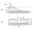
図2は、ダイシングブレード30と、カットする対象となる基板との関係を示す図である。この図2及び後述する図3(b)に示すように、ダイシングブレード30は、例えば、ダイシングテープ16の途中まで、ダイシングテープ16の上面を浅く切る程度に、半導体層12、シリコン基板10及びメタル層14をダイシングするように設置され、基板全体をダイシングする。
FIG. 2 is a diagram showing the relationship between the
ダイシングブレード30は、その刃部32がメタルの切断とシリコンの切断に適しているものを利用する。この刃部32によりメタル層14及びシリコンを切断するようにダイシングを行う。上述したように、この切断においては、ダイシングテープ16の上面も浅く切断される。
The
図3(a)及び図3(b)は、ダイシングのタイミングにおける基板とダイシングブレード30との様子を示す図である。それぞれ、図2に示す方向A及び方向Bから見た図、すなわち、ダイシングブレード30と垂直な方向及びダイシングブレード30と平行な方向からの様子を示す図である。
FIGS. 3A and 3B are views showing the state of the substrate and the
図3(a)に示すように、ダイシングブレード30の刃部32は、少なくともメタル層14と、半導体層12と、シリコン基板10と、を切断し、ダイシングテープ16の上面を浅く切断するのに問題の無い長さを有している。この刃部32により半導体層12及びシリコン層10と、メタル層14と、ダイシングテープ16の上面とが一緒に切断される。ダイシングブレードの幅は、本実施形態においては、厚いところで15〜50μmであるが、少なくともメタル層14を切っている部位は、刃先に曲率を有しているため、ダイシングブレードの元厚の部位よりも薄くなっている。また、切込み深さにより、メタル部のダイシングカーフ幅は変わっている。
As shown in FIG. 3A, the
図3(b)は、方向Bから見たダイシングブレード30の断面を示す図である。なお、ダイシングブレード30の素材は特に限られるものではないので、この図3(b)において、ハッチングは省略している。
FIG. 3B is a view showing a cross section of the
この図3(b)に示すように、ダイシングブレード30の刃部32の側面部34は、シリコン基板10の高さの途中から曲線を描くような曲率を有している。この曲率は、図3(b)に示すように、なめらかな曲率をしている。
As shown in FIG. 3B, the side surface portion 34 of the
ダイシングブレード30において、刃部32は、例えば、メタルの切断とシリコン基板10の切断との両方に適するように選んだダイヤモンドの粒子を有している。
In the
別の例として、このダイシングブレード30を、ダイシングテープ16の途中まで到達するような通常の使用法により用いるのではなく、メタル層14の下面14bまでを切断し、ダイシングテープ16の上面付近を刃部32の刃先が切断する程度の高さにダイシングブレード30の高さを調整することによって、半導体装置1の下部において図1(e)に示すように曲率を有するように切断をすることが可能となる。すなわち、図3(a)に示すよりも高い位置であり、かつ、メタル層14が切断されるようにさらに浅い位置にダイシングソーの刃部32が配置されるように制御してもよい。
As another example, the
このように、本実施形態においては、メタル層14までが切断され、さらに、刃部32の側面が有している曲率が半導体装置1の側面の曲率に転写されるように、シングルカットによりダイシングされるものであればよい。
As described above, in the present embodiment, the
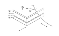
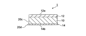
図4は、本実施形態に係る半導体装置1の断面を示す図である。この図4に示すように、半導体装置1は、メタル層14と、シリコン基板10と、半導体層12とが重なり合うように形成されている。その側面は、シリコン基板10における側面20bが途中から曲率を有し、メタル層14の側面20aへと曲率を有したまま接続される。換言すると、半導体装置1の側面は、シリコン基板10の側面の上方から下方へと向かって平面視における半導体装置1の面積が増していくような曲率を有し、シリコン基板10の下面10bに接しているメタル層14の下方へと向かってさらに拡がるような曲率を有する。ダイシングソーの刃部32は、個体差により、その側面が厳密に平面であるわけではないので、当該刃部32の形状に合わせ、側面20bは、厳密に平面上の部分と曲率を有する部分とが分離されるのではなく、全体的になだらかな曲率を有していてもよい。
FIG. 4 is a view showing a cross section of the
この図4の半導体装置1は、図1(e)に示す基板から、1チップ分を取り出したものであり、メタル層14の下面14bからダイシングテープ16を除去したものである。この状態において、例えば、チップをダイボンディングして、その後、ワイヤボンディング、モールド等の工程を経ることにより半導体パッケージが生成される。
The
この図4に示すように、断面において、メタル層14の下面14bの長さが、半導体層12の上面12aの長さよりも長くなるように、半導体装置1は、形成される。3次元空間で表現すると、一例として、チップは矩形状であり、メタル層14の下面14bの面積が、半導体層12の上面12aの面積よりも広くなるように形成される。また、メタル層14の下面14bの各辺の長さが、対応する半導体層12の上面12aの各辺の長さよりも長くなるように形成される。
As shown in FIG. 4, the
このように、上面に比べて下面の面積を広くすることにより、ダイシング後においてチップを並べて搬送する場合等に、チップ表面(すなわち、上面12a)同士の距離を稼ぐことが可能となるため、チップ表面におけるチップ同士の接触する可能性が低くなる。このため、チップ同士の衝突によるチップ欠け、表面チッピングが発生しづらくなり、チップの品質が向上する。この結果、ボンディング不良の低減、抗折強度の低下の抑制をすることが可能となる。
Thus, by increasing the area of the lower surface compared to the upper surface, it becomes possible to increase the distance between the chip surfaces (that is, the
ここで、チッピングとは、各面において表面が割れたり、ヒビが入ったり、欠けたりすることを言う。このチッピングが起こることにより、搬送時、加工時及び使用時における半導体装置1の性能が低下する。
Here, chipping means that the surface is cracked, cracked or chipped on each surface. When this chipping occurs, the performance of the
図5は、半導体装置1を支持基盤40にダイボンディングした様子を示すものである。例えば、メタル層14が支持基盤40上にはんだ42を用いてボンディングされている。この図5に示すように、半導体装置1の側面が曲率を有することにより、側面が垂直である場合と比較してはんだ42とメタル層14との接触面が広くなる。この結果、ダイシェア強度の向上、すなわち、ダイボンディング性を向上することが可能となる。はんだ42でボンディングする場合に限られず、ダイボンディング樹脂によりボンディングされる場合も同様である。
FIG. 5 shows a state where the
さらに、図5に示すように曲率を有していると、はんだ42でダイボンディングを行う場合に、メタル層14の側面が垂直になっている場合と比べて、はんだ42とメタル層14との接続面積が大きくなる。このことから、半導体装置1の表面までの側面の距離が長くなり、メタル層14と半導体層12が側面においてショートすること、さらには、メタル層14と半導体層12の表面とがショートすること、表面の半導体層12内の配線とボンディングに用いるはんだとがショートすることを抑制することが可能となる。同様の理由から、はんだ42を介した半導体装置1の側面からのリーク電流を抑制することが可能となる。
Furthermore, as shown in FIG. 5, when the
ただし、メタル層14の下面14bが半導体層12の上面12aよりも長くなる長さが、半導体装置1の厚さの25%程度を越えると、チップとしての必要となる面積が広くなり、また、側面の曲率が緩くなり、さらに、ダイシングブレード30の形状も特殊なものとなるので、好ましくない。より好ましくは、メタル層14の下面14bが半導体層12の上面12aよりもせり出している長さは、半導体装置1の厚さの5%から25%程度であることが望ましい。
However, if the length by which the
以上のように、本実施形態によれば、側面に上面から下面へと向かって曲率を有し、上面よりも下面の面積を広くした形状を有することにより、リーク電流を抑制した上で、ダイボンディングの強度を向上することが可能となる。また、表面までの距離が長いため、側面におけるショートが発生しづらくなる。メタル層14と側面とのショートを発生させなくすることにより、メタル層14と半導体装置1の配線層等の表面とのショート、及び半導体装置1の側面と表面とのショートをも抑制できる。さらに、チップ表面の距離を長く保つことが可能となるため、ダイシング後の搬送時にチップ同士の衝突が発生しづらくなり、チップの品質を向上することが可能となる。
As described above, according to the present embodiment, the side surface has a curvature from the upper surface to the lower surface, and the lower surface has a larger area than the upper surface. It is possible to improve the bonding strength. In addition, since the distance to the surface is long, short-circuiting on the side surface is difficult to occur. By preventing the short circuit between the
一般的には、シリコンとメタルを別々に切断することが多いが、本実施形態においては1本のダイシングブレードを用いて切断している。この結果、ダイシングの工程におけるスループットを上げることが可能となる。このスループットはデュアルカットにするとより上げることが可能である。 In general, silicon and metal are often cut separately, but in this embodiment, cutting is performed using one dicing blade. As a result, the throughput in the dicing process can be increased. This throughput can be further increased by dual cut.
なお、上記では、半導体装置1の下層は、メタル層14であるもととしたが、これはダイアタッチフィルムであってもよい。ダイアタッチフィルムは、例えば、導電性のダイアタッチフィルムであってもよい。ダイアタッチフィルムを用いた半導体装置1を形成することにより、積層して半導体パッケージを製造する場合に、半導体装置1に加工を施すことなく積層させることが可能となる。
In the above description, the lower layer of the
(変形例)
前述した実施形態においては、シングルカットでダイシングを行ったが、これには限られず、ステップカットでダイシングを行うようにしてもよい。
(Modification)
In the embodiment described above, dicing is performed by single cut. However, the present invention is not limited to this, and dicing may be performed by step cut.
すなわち、本変形例においては、シリコン基板10を切断するダイシングブレードと、メタル層14を切断するダイシングブレードとを別々に用意し、それぞれの層により適したダイシングブレードにより切断を行う。すなわち、シリコン基板10は、シリコンを切断するダイシングブレード30の刃部32で切断し、メタル層14は、メタルを切断するダイシングブレード30の刃部32により切断をするようにしてもよい。
That is, in this modification, a dicing blade that cuts the
図6は、ステップカットにより形成された半導体装置1を示す図である。本変形例に係る半導体装置1は、前工程後の基板に対して、まず、シリコンを切断する第1のダイシングブレードを用いて、シリコン基板10の下面10bを貫通する深さまで第1の切断を行う。この第1の切断は、メタル層14の上面14aに到達してもよいが、メタル層14の切断を目的としたものではないので、メタル層14を完全に切断するものではない。
FIG. 6 is a diagram illustrating the
第1の切断を行った後に、第1の切断面に表出したメタル層14に対して、第1のダイシングブレードよりも刃幅の狭い第2のダイシングブレードを用いて、メタル層14の下面14bまでを切断するように、第2の切断を行う。この第2の切断は、前述した実施形態と同様に、ダイシングテープ16の上面を浅く切断してもよい。
After performing the first cutting, a lower surface of the
図6に示すように、第1の切断においては、前述した実施形態に係る半導体装置1と同様に、側面20cに曲率を有するように切断される。これは、ダイシングブレードの断面形状と同様にシリコン基板10までが切断されるためである。続く第2の切断においては、メタル層14を垂直に、もしくは、本変形例においても、図4又は図7に示すように、前述した実施形態と同様に曲率を持った断面となるように側面20dが表出するように切断される。
As shown in FIG. 6, in the first cutting, similarly to the
図7は、図6の変形例に係る半導体装置1を示す図である。図7のような切断面は、メタル層14の切断を行う際に、前述の実施形態で説明したように、メタル層14の下面14bまでを切断するようにダイシングブレードの高さを調節することにより形成される。上述したように、ダイシングテープ16の途中まで、ダイシングテープ16の上面を浅く切断する程度の高さに調節するようにしてもよい。
FIG. 7 is a diagram showing a
図8は、本実施形態の別の例に係る半導体装置1を示す図である。この図8に示すように、ほぼ垂直である部分が、シリコン基板10の下方に及んでいてもよい。このような場合においても、図6等と同様の効果を得ることが可能となる。
FIG. 8 is a diagram illustrating a
図9は、さらに別の例に係る半導体装置1を示す図である。この図9に示すように、シリコン層10を切断する際に、メタル層14の上層部をも切断してもよい。
FIG. 9 is a diagram illustrating a
以上のように、本変形例によっても、側面20cにおいて曲率を有するため、前述した実施形態に係る半導体装置1と同様に、上面12aよりも下面14bの面積が広く、チップ形状、すなわち、半導体1の形状が矩形である場合には、上面12aの各辺の長さよりも、下面14bの各辺の長さが長くなる。この長さの差により、半導体装置1の上面12aの衝突を抑制することが可能となる。ステップカットにすることにより、前述のシングルカットに比べて、メタル用、シリコン用のブレードの選定をすることが可能となり、さらなる品質向上につながる。
As described above, according to the present modification as well, since the
すなわち、シリコン基板10及びメタル層14を切断する刃が異なるため、ダイシング工程において、シリコン基板10の表面及び側面チッピング及びメタル層14の下面14bにおける裏面チッピングの発生を抑制し、抗折強度を向上することに繋がり、チップの歩留まりを向上させることが可能となる。また、たとえシリコン層10の下部においてヒビ等のクラックが発生した場合においても、チッピングが発生したシリコン層10の下面と当該メタル層14の上面とが物理的に接続し、当該チッピング箇所は、少なくともその下面においてメタル層10に固定されているため、チッピング部分の剥がれが発生しづらくなり、後工程におけるゴミを発生させることを抑制することが可能となる。
That is, since the blades for cutting the
また、側面20dが垂直である場合においても、側面20dにおいては、はんだ、ダイボンディング樹脂等のボンディング剤に対して従来のものと効果は変わらないが、側面20cにおいて曲率を有するため、ボンディング剤が側面20cの側面を上から押さえつける力が前述の実施形態と同様に掛かるため、同様の効果を得ることが可能となる。はんだ等の導電体のボンディング剤である場合はさらに、前述の実施形態と同様に、側面又は表面における電流のリークを抑制することも可能となる。
Even when the
本発明のいくつかの実施形態を説明したが、これらの実施形態は、例として提示したものであり、発明の範囲を限定することは意図していない。これら新規な実施形態は、その他の様々な形態で実施されることが可能であり、発明の要旨を逸脱しない範囲で種々の省略、置き換え、変更を行うことができる。これら実施形態やその変形は、発明の範囲や要旨に含まれるとともに、特許請求の範囲に記載された発明とその均等の範囲に含まれる。また、当然のことながら、本発明の要旨の範囲内で、これらの実施の形態を部分的に適宜組み合わせることも可能である。 Although several embodiments of the present invention have been described, these embodiments are presented by way of example and are not intended to limit the scope of the invention. These novel embodiments can be implemented in various other forms, and various omissions, replacements, and changes can be made without departing from the scope of the invention. These embodiments and modifications thereof are included in the scope and gist of the invention, and are included in the invention described in the claims and the equivalents thereof. Of course, it is possible to appropriately combine these embodiments partially within the scope of the present invention.
例えば、半導体装置1は、それぞれ交わる方向に基板が切断されてチップ化されるが、一方の方向においては、シングルカットにより切断され、他方の方向においては、ステップカットにより切断されてもよい。もちろん、双方の方向においてシングルカット又はステップカットにより切断されてもよい。さらには、対向する2組の側面のうち、1組の側面のみが上述したように曲率を有していてもよい。
For example, the
また、半導体装置1のシリコン基板10は、別のもので置き換えられたものであってもよい。例えば、窒化ガリウム(GaN)、炭化ケイ素(SiC)等を用いた基板であっても、当然前述の実施形態に係るダイシング方法により、半導体装置1と同様の効果を得ることが可能となる。
Further, the
さらに、図10のように、メタル層14の途中から側面に曲率を有するように半導体装置1を形成してもよい。このように、メタル層14の厚さにより、シリコン基板10及びメタル層14におけるカーブの位置が変化しても構わない。
Further, as shown in FIG. 10, the
前述の半導体装置1の形状は、例えば、顕微鏡等を用いてチップの断面を観察すること、又は、側面を観察することにより検知することが可能である。
The shape of the
1:半導体装置、10:シリコン基板、12:半導体層、14:メタル層、16:ダイシングテープ、20a、20b、20c、20d:側面、30:ダイシングブレード、32:刃部、40:支持基盤、42:はんだ 1: Semiconductor device, 10: Silicon substrate, 12: Semiconductor layer, 14: Metal layer, 16: Dicing tape, 20a, 20b, 20c, 20d: Side surface, 30: Dicing blade, 32: Blade part, 40: Support base, 42: Solder
Claims (11)
前記シリコン基板の上面に形成された、半導体層と、
前記シリコン基板の下面に形成され、その側面が前記シリコン基板の側面と接続する、下層と、
を備え、少なくとも1対の側面が上方から下方へ向かって拡がるカーブ形状を有する、半導体装置。 A silicon substrate;
A semiconductor layer formed on the upper surface of the silicon substrate;
A lower layer formed on the lower surface of the silicon substrate, the side surface of which is connected to the side surface of the silicon substrate;
A semiconductor device having a curved shape in which at least one pair of side surfaces expands from above to below.
シリコン基板に前記ダイシングブレードを接触させるステップと、
前記シリコン基板と、当該シリコン基板の上面に形成された半導体層と、当該シリコン基板の下面に形成された下層とを、その上方から下方へと向かって拡がるような側面を有するように、ダイシングをするステップと、
を備える半導体装置のダイシング方法。 Rotating the dicing blade;
Contacting the dicing blade with a silicon substrate;
Dicing so that the silicon substrate, the semiconductor layer formed on the upper surface of the silicon substrate, and the lower layer formed on the lower surface of the silicon substrate have side surfaces that extend from the upper side to the lower side. And steps to
A dicing method for a semiconductor device comprising:
前記シリコン基板及び前記半導体層を、前記シリコン基板が、その上方から下方へと向かって拡がるような側面を有するように切断するステップと、
前記下層を、当該下層の下面の面積が、前記半導体層の上面の面積よりも広い面積となるように切断するステップと、
を備える、請求項8に記載のダイシング方法。 The dicing step includes
Cutting the silicon substrate and the semiconductor layer so that the silicon substrate has a side surface extending from the upper side to the lower side;
Cutting the lower layer such that the area of the lower surface of the lower layer is larger than the area of the upper surface of the semiconductor layer;
The dicing method according to claim 8, comprising:
Priority Applications (4)
| Application Number | Priority Date | Filing Date | Title |
|---|---|---|---|
| JP2018033567A JP2019149472A (en) | 2018-02-27 | 2018-02-27 | Semiconductor device and dicing method |
| CN201810182302.3A CN110197815B (en) | 2018-02-27 | 2018-03-06 | Semiconductor device and dicing method |
| US15/918,141 US10784165B2 (en) | 2018-02-27 | 2018-03-12 | Semiconductor device and dicing method |
| JP2021132976A JP7240455B2 (en) | 2018-02-27 | 2021-08-17 | Semiconductor device and dicing method |
Applications Claiming Priority (1)
| Application Number | Priority Date | Filing Date | Title |
|---|---|---|---|
| JP2018033567A JP2019149472A (en) | 2018-02-27 | 2018-02-27 | Semiconductor device and dicing method |
Related Child Applications (1)
| Application Number | Title | Priority Date | Filing Date |
|---|---|---|---|
| JP2021132976A Division JP7240455B2 (en) | 2018-02-27 | 2021-08-17 | Semiconductor device and dicing method |
Publications (2)
| Publication Number | Publication Date |
|---|---|
| JP2019149472A true JP2019149472A (en) | 2019-09-05 |
| JP2019149472A5 JP2019149472A5 (en) | 2020-02-20 |
Family
ID=67684945
Family Applications (2)
| Application Number | Title | Priority Date | Filing Date |
|---|---|---|---|
| JP2018033567A Pending JP2019149472A (en) | 2018-02-27 | 2018-02-27 | Semiconductor device and dicing method |
| JP2021132976A Active JP7240455B2 (en) | 2018-02-27 | 2021-08-17 | Semiconductor device and dicing method |
Family Applications After (1)
| Application Number | Title | Priority Date | Filing Date |
|---|---|---|---|
| JP2021132976A Active JP7240455B2 (en) | 2018-02-27 | 2021-08-17 | Semiconductor device and dicing method |
Country Status (3)
| Country | Link |
|---|---|
| US (1) | US10784165B2 (en) |
| JP (2) | JP2019149472A (en) |
| CN (1) | CN110197815B (en) |
Families Citing this family (2)
| Publication number | Priority date | Publication date | Assignee | Title |
|---|---|---|---|---|
| JP7100980B2 (en) | 2018-01-22 | 2022-07-14 | ローム株式会社 | LED package |
| JP7135352B2 (en) * | 2018-03-14 | 2022-09-13 | 富士電機株式会社 | Semiconductor device manufacturing method |
Citations (8)
| Publication number | Priority date | Publication date | Assignee | Title |
|---|---|---|---|---|
| JPH02220811A (en) * | 1989-02-23 | 1990-09-04 | Nippon Inter Electronics Corp | Production of semiconductor device |
| JP2005243947A (en) * | 2004-02-26 | 2005-09-08 | Sumitomo Electric Ind Ltd | Method for manufacturing semiconductor device, and semiconductor device |
| JP2008252081A (en) * | 2007-03-05 | 2008-10-16 | Hitachi Chem Co Ltd | Method of manufacturing semiconductor device |
| JP2010171156A (en) * | 2009-01-22 | 2010-08-05 | Renesas Electronics Corp | Semiconductor device and manufacturing method of semiconductor device |
| JP2011060807A (en) * | 2009-09-07 | 2011-03-24 | Renesas Electronics Corp | Semiconductor chip with conductive adhesive layer and method of manufacturing the same, and method of manufacturing semiconductor device |
| JP2013004528A (en) * | 2011-06-10 | 2013-01-07 | Panasonic Corp | Semiconductor device and manufacturing method of the same |
| JP2016201533A (en) * | 2015-04-07 | 2016-12-01 | 株式会社東芝 | Semiconductor device manufacturing method |
| JP2017041525A (en) * | 2015-08-19 | 2017-02-23 | 株式会社ディスコ | Wafer division method |
Family Cites Families (24)
| Publication number | Priority date | Publication date | Assignee | Title |
|---|---|---|---|---|
| JPH02271558A (en) * | 1989-04-12 | 1990-11-06 | Mitsubishi Electric Corp | Semiconductor device and its manufacture |
| DE19632626A1 (en) * | 1996-08-13 | 1998-02-19 | Siemens Ag | Method for manufacturing semiconductor bodies with MOVPE layer sequence |
| US6294439B1 (en) * | 1997-07-23 | 2001-09-25 | Kabushiki Kaisha Toshiba | Method of dividing a wafer and method of manufacturing a semiconductor device |
| JP3497722B2 (en) * | 1998-02-27 | 2004-02-16 | 富士通株式会社 | Semiconductor device, method of manufacturing the same, and transfer tray thereof |
| JP2002164388A (en) | 2000-11-28 | 2002-06-07 | Toshiba Chem Corp | Semiconductor device and its manufacturing method |
| JP2003158097A (en) | 2001-11-22 | 2003-05-30 | Murata Mfg Co Ltd | Semiconductor device and manufacturing method therefor |
| JP2004158739A (en) | 2002-11-08 | 2004-06-03 | Toshiba Corp | Resin sealed semiconductor device and manufacturing method therefor |
| JP4241284B2 (en) | 2003-09-19 | 2009-03-18 | カシオ計算機株式会社 | Semiconductor device |
| US8802465B2 (en) * | 2005-01-11 | 2014-08-12 | SemiLEDs Optoelectronics Co., Ltd. | Method for handling a semiconductor wafer assembly |
| JP2006196809A (en) | 2005-01-17 | 2006-07-27 | Sony Corp | Semiconductor chip, method for manufacturing same and semiconductor device |
| JP2006344816A (en) | 2005-06-09 | 2006-12-21 | Matsushita Electric Ind Co Ltd | Method of manufacturing semiconductor chip |
| JP4719042B2 (en) | 2006-03-16 | 2011-07-06 | 株式会社東芝 | Manufacturing method of semiconductor device |
| US10505083B2 (en) * | 2007-07-11 | 2019-12-10 | Cree, Inc. | Coating method utilizing phosphor containment structure and devices fabricated using same |
| JP5237764B2 (en) | 2008-11-10 | 2013-07-17 | スタンレー電気株式会社 | Manufacturing method of semiconductor device |
| JP2010225648A (en) * | 2009-03-19 | 2010-10-07 | Casio Computer Co Ltd | Semiconductor device and method of manufacturing the same |
| JP2011035245A (en) * | 2009-08-04 | 2011-02-17 | Disco Abrasive Syst Ltd | Method for dividing plate-shaped work |
| WO2011145794A1 (en) * | 2010-05-18 | 2011-11-24 | 서울반도체 주식회사 | Light emitting diode chip having wavelength conversion layer and manufacturing method thereof, and package including same and manufacturing method thereof |
| TWI569385B (en) | 2011-05-27 | 2017-02-01 | 住友電木股份有限公司 | Manufacturing method of semiconductor device |
| US8647966B2 (en) | 2011-06-09 | 2014-02-11 | National Semiconductor Corporation | Method and apparatus for dicing die attach film on a semiconductor wafer |
| JP2015138857A (en) | 2014-01-22 | 2015-07-30 | 株式会社ディスコ | Wafer processing method |
| JP2016018846A (en) | 2014-07-07 | 2016-02-01 | 株式会社東芝 | Semiconductor package, and method of manufacturing the same |
| US9385268B2 (en) * | 2014-11-10 | 2016-07-05 | Fuji Xerox Co., Ltd. | Method of manufacturing semiconductor chips |
| JP2016201505A (en) | 2015-04-14 | 2016-12-01 | トヨタ自動車株式会社 | Semiconductor device |
| JP2017054861A (en) * | 2015-09-07 | 2017-03-16 | 株式会社東芝 | Method of manufacturing semiconductor device |
-
2018
- 2018-02-27 JP JP2018033567A patent/JP2019149472A/en active Pending
- 2018-03-06 CN CN201810182302.3A patent/CN110197815B/en active Active
- 2018-03-12 US US15/918,141 patent/US10784165B2/en active Active
-
2021
- 2021-08-17 JP JP2021132976A patent/JP7240455B2/en active Active
Patent Citations (8)
| Publication number | Priority date | Publication date | Assignee | Title |
|---|---|---|---|---|
| JPH02220811A (en) * | 1989-02-23 | 1990-09-04 | Nippon Inter Electronics Corp | Production of semiconductor device |
| JP2005243947A (en) * | 2004-02-26 | 2005-09-08 | Sumitomo Electric Ind Ltd | Method for manufacturing semiconductor device, and semiconductor device |
| JP2008252081A (en) * | 2007-03-05 | 2008-10-16 | Hitachi Chem Co Ltd | Method of manufacturing semiconductor device |
| JP2010171156A (en) * | 2009-01-22 | 2010-08-05 | Renesas Electronics Corp | Semiconductor device and manufacturing method of semiconductor device |
| JP2011060807A (en) * | 2009-09-07 | 2011-03-24 | Renesas Electronics Corp | Semiconductor chip with conductive adhesive layer and method of manufacturing the same, and method of manufacturing semiconductor device |
| JP2013004528A (en) * | 2011-06-10 | 2013-01-07 | Panasonic Corp | Semiconductor device and manufacturing method of the same |
| JP2016201533A (en) * | 2015-04-07 | 2016-12-01 | 株式会社東芝 | Semiconductor device manufacturing method |
| JP2017041525A (en) * | 2015-08-19 | 2017-02-23 | 株式会社ディスコ | Wafer division method |
Also Published As
| Publication number | Publication date |
|---|---|
| US10784165B2 (en) | 2020-09-22 |
| CN110197815A (en) | 2019-09-03 |
| JP2021180338A (en) | 2021-11-18 |
| CN110197815B (en) | 2023-08-22 |
| US20190267288A1 (en) | 2019-08-29 |
| JP7240455B2 (en) | 2023-03-15 |
Similar Documents
| Publication | Publication Date | Title |
|---|---|---|
| KR101366949B1 (en) | Through silicon via guard ring | |
| JP7240455B2 (en) | Semiconductor device and dicing method | |
| KR100605433B1 (en) | Semiconductor device and method for manufacturing thereof | |
| CN110970358B (en) | Stacked semiconductor device and method of manufacturing the same | |
| JP2011223049A (en) | Method of removing substrate for high light extraction led | |
| US11062969B2 (en) | Wafer level chip scale package structure and manufacturing method thereof | |
| US9490103B2 (en) | Separation of chips on a substrate | |
| JP2018139263A (en) | Semiconductor package and manufacturing method of the same | |
| JP6100396B2 (en) | Semiconductor device manufacturing method and semiconductor device | |
| JP2004146487A (en) | Method for manufacturing semiconductor device | |
| JP6190953B2 (en) | Semiconductor wafer, semiconductor device separated from semiconductor wafer, and method of manufacturing semiconductor device | |
| US9269676B2 (en) | Through silicon via guard ring | |
| JP2010171371A (en) | Method for producing group-iii nitride-based compound semiconductor element | |
| JP2013058707A (en) | Semiconductor light-emitting element manufacturing method | |
| CN111092051A (en) | Semiconductor package and method of manufacturing the same | |
| JP2005044901A (en) | Semiconductor wafer dividing method | |
| JP2010135565A (en) | Semiconductor device and production process of the same | |
| JP4406329B2 (en) | Semiconductor device and manufacturing method thereof | |
| JPH06151583A (en) | Compound semiconductor wafer | |
| JP7399834B2 (en) | Semiconductor device and its manufacturing method | |
| KR102649711B1 (en) | Method for manufacturing ultra-thin type semiconductor die | |
| Ma et al. | Wafer Thinning and Dicing Technology for 3D Nand Flash | |
| JP2023090362A (en) | Manufacturing method of semiconductor device | |
| CN115841944A (en) | Semiconductor device and method for manufacturing the same |
Legal Events
| Date | Code | Title | Description |
|---|---|---|---|
| A521 | Request for written amendment filed |
Free format text: JAPANESE INTERMEDIATE CODE: A523 Effective date: 20200110 |
|
| A621 | Written request for application examination |
Free format text: JAPANESE INTERMEDIATE CODE: A621 Effective date: 20200110 |
|
| A977 | Report on retrieval |
Free format text: JAPANESE INTERMEDIATE CODE: A971007 Effective date: 20201127 |
|
| A131 | Notification of reasons for refusal |
Free format text: JAPANESE INTERMEDIATE CODE: A131 Effective date: 20201211 |
|
| A521 | Request for written amendment filed |
Free format text: JAPANESE INTERMEDIATE CODE: A523 Effective date: 20210126 |
|
| A131 | Notification of reasons for refusal |
Free format text: JAPANESE INTERMEDIATE CODE: A131 Effective date: 20210226 |
|
| A521 | Request for written amendment filed |
Free format text: JAPANESE INTERMEDIATE CODE: A523 Effective date: 20210412 |
|
| A02 | Decision of refusal |
Free format text: JAPANESE INTERMEDIATE CODE: A02 Effective date: 20210525 |