JP2019128152A - Semiconductor device and optical encoder - Google Patents
Semiconductor device and optical encoder Download PDFInfo
- Publication number
- JP2019128152A JP2019128152A JP2018007590A JP2018007590A JP2019128152A JP 2019128152 A JP2019128152 A JP 2019128152A JP 2018007590 A JP2018007590 A JP 2018007590A JP 2018007590 A JP2018007590 A JP 2018007590A JP 2019128152 A JP2019128152 A JP 2019128152A
- Authority
- JP
- Japan
- Prior art keywords
- light source
- photoelectric conversion
- unit
- signal
- semiconductor device
- Prior art date
- Legal status (The legal status is an assumption and is not a legal conclusion. Google has not performed a legal analysis and makes no representation as to the accuracy of the status listed.)
- Granted
Links
- 239000004065 semiconductor Substances 0.000 title claims abstract description 68
- 230000003287 optical effect Effects 0.000 title claims description 8
- 238000006243 chemical reaction Methods 0.000 claims abstract description 124
- 239000000758 substrate Substances 0.000 claims abstract description 17
- 239000012535 impurity Substances 0.000 claims description 21
- 239000000463 material Substances 0.000 claims description 10
- 238000001514 detection method Methods 0.000 claims description 7
- 238000013459 approach Methods 0.000 claims description 3
- 230000008859 change Effects 0.000 claims description 3
- 238000000034 method Methods 0.000 abstract description 2
- 101000806846 Homo sapiens DNA-(apurinic or apyrimidinic site) endonuclease Proteins 0.000 description 13
- 101000835083 Homo sapiens Tissue factor pathway inhibitor 2 Proteins 0.000 description 13
- 102100026134 Tissue factor pathway inhibitor 2 Human genes 0.000 description 13
- 238000010586 diagram Methods 0.000 description 3
- 238000002513 implantation Methods 0.000 description 3
- 238000004519 manufacturing process Methods 0.000 description 3
- 239000002184 metal Substances 0.000 description 2
- 239000000969 carrier Substances 0.000 description 1
- 230000001771 impaired effect Effects 0.000 description 1
- 238000007689 inspection Methods 0.000 description 1
- 238000010030 laminating Methods 0.000 description 1
- 238000012986 modification Methods 0.000 description 1
- 230000004048 modification Effects 0.000 description 1
- 230000035515 penetration Effects 0.000 description 1
- 230000002093 peripheral effect Effects 0.000 description 1
- 230000009467 reduction Effects 0.000 description 1
- 230000004044 response Effects 0.000 description 1
- 238000000638 solvent extraction Methods 0.000 description 1
Images


Classifications
-
- G—PHYSICS
- G01—MEASURING; TESTING
- G01D—MEASURING NOT SPECIALLY ADAPTED FOR A SPECIFIC VARIABLE; ARRANGEMENTS FOR MEASURING TWO OR MORE VARIABLES NOT COVERED IN A SINGLE OTHER SUBCLASS; TARIFF METERING APPARATUS; MEASURING OR TESTING NOT OTHERWISE PROVIDED FOR
- G01D5/00—Mechanical means for transferring the output of a sensing member; Means for converting the output of a sensing member to another variable where the form or nature of the sensing member does not constrain the means for converting; Transducers not specially adapted for a specific variable
- G01D5/26—Mechanical means for transferring the output of a sensing member; Means for converting the output of a sensing member to another variable where the form or nature of the sensing member does not constrain the means for converting; Transducers not specially adapted for a specific variable characterised by optical transfer means, i.e. using infrared, visible, or ultraviolet light
- G01D5/32—Mechanical means for transferring the output of a sensing member; Means for converting the output of a sensing member to another variable where the form or nature of the sensing member does not constrain the means for converting; Transducers not specially adapted for a specific variable characterised by optical transfer means, i.e. using infrared, visible, or ultraviolet light with attenuation or whole or partial obturation of beams of light
- G01D5/34—Mechanical means for transferring the output of a sensing member; Means for converting the output of a sensing member to another variable where the form or nature of the sensing member does not constrain the means for converting; Transducers not specially adapted for a specific variable characterised by optical transfer means, i.e. using infrared, visible, or ultraviolet light with attenuation or whole or partial obturation of beams of light the beams of light being detected by photocells
- G01D5/347—Mechanical means for transferring the output of a sensing member; Means for converting the output of a sensing member to another variable where the form or nature of the sensing member does not constrain the means for converting; Transducers not specially adapted for a specific variable characterised by optical transfer means, i.e. using infrared, visible, or ultraviolet light with attenuation or whole or partial obturation of beams of light the beams of light being detected by photocells using displacement encoding scales
- G01D5/34707—Scales; Discs, e.g. fixation, fabrication, compensation
- G01D5/34715—Scale reading or illumination devices
-
- G—PHYSICS
- G01—MEASURING; TESTING
- G01D—MEASURING NOT SPECIALLY ADAPTED FOR A SPECIFIC VARIABLE; ARRANGEMENTS FOR MEASURING TWO OR MORE VARIABLES NOT COVERED IN A SINGLE OTHER SUBCLASS; TARIFF METERING APPARATUS; MEASURING OR TESTING NOT OTHERWISE PROVIDED FOR
- G01D5/00—Mechanical means for transferring the output of a sensing member; Means for converting the output of a sensing member to another variable where the form or nature of the sensing member does not constrain the means for converting; Transducers not specially adapted for a specific variable
- G01D5/12—Mechanical means for transferring the output of a sensing member; Means for converting the output of a sensing member to another variable where the form or nature of the sensing member does not constrain the means for converting; Transducers not specially adapted for a specific variable using electric or magnetic means
- G01D5/244—Mechanical means for transferring the output of a sensing member; Means for converting the output of a sensing member to another variable where the form or nature of the sensing member does not constrain the means for converting; Transducers not specially adapted for a specific variable using electric or magnetic means influencing characteristics of pulses or pulse trains; generating pulses or pulse trains
- G01D5/24428—Error prevention
-
- G—PHYSICS
- G01—MEASURING; TESTING
- G01J—MEASUREMENT OF INTENSITY, VELOCITY, SPECTRAL CONTENT, POLARISATION, PHASE OR PULSE CHARACTERISTICS OF INFRARED, VISIBLE OR ULTRAVIOLET LIGHT; COLORIMETRY; RADIATION PYROMETRY
- G01J1/00—Photometry, e.g. photographic exposure meter
- G01J1/10—Photometry, e.g. photographic exposure meter by comparison with reference light or electric value provisionally void
- G01J1/16—Photometry, e.g. photographic exposure meter by comparison with reference light or electric value provisionally void using electric radiation detectors
- G01J1/1626—Arrangements with two photodetectors, the signals of which are compared
-
- G—PHYSICS
- G01—MEASURING; TESTING
- G01J—MEASUREMENT OF INTENSITY, VELOCITY, SPECTRAL CONTENT, POLARISATION, PHASE OR PULSE CHARACTERISTICS OF INFRARED, VISIBLE OR ULTRAVIOLET LIGHT; COLORIMETRY; RADIATION PYROMETRY
- G01J1/00—Photometry, e.g. photographic exposure meter
- G01J1/10—Photometry, e.g. photographic exposure meter by comparison with reference light or electric value provisionally void
- G01J1/20—Photometry, e.g. photographic exposure meter by comparison with reference light or electric value provisionally void intensity of the measured or reference value being varied to equalise their effects at the detectors, e.g. by varying incidence angle
- G01J1/28—Photometry, e.g. photographic exposure meter by comparison with reference light or electric value provisionally void intensity of the measured or reference value being varied to equalise their effects at the detectors, e.g. by varying incidence angle using variation of intensity or distance of source
- G01J1/30—Photometry, e.g. photographic exposure meter by comparison with reference light or electric value provisionally void intensity of the measured or reference value being varied to equalise their effects at the detectors, e.g. by varying incidence angle using variation of intensity or distance of source using electric radiation detectors
- G01J1/32—Photometry, e.g. photographic exposure meter by comparison with reference light or electric value provisionally void intensity of the measured or reference value being varied to equalise their effects at the detectors, e.g. by varying incidence angle using variation of intensity or distance of source using electric radiation detectors adapted for automatic variation of the measured or reference value
-
- G—PHYSICS
- G01—MEASURING; TESTING
- G01J—MEASUREMENT OF INTENSITY, VELOCITY, SPECTRAL CONTENT, POLARISATION, PHASE OR PULSE CHARACTERISTICS OF INFRARED, VISIBLE OR ULTRAVIOLET LIGHT; COLORIMETRY; RADIATION PYROMETRY
- G01J1/00—Photometry, e.g. photographic exposure meter
- G01J1/42—Photometry, e.g. photographic exposure meter using electric radiation detectors
- G01J1/44—Electric circuits
-
- G—PHYSICS
- G01—MEASURING; TESTING
- G01D—MEASURING NOT SPECIALLY ADAPTED FOR A SPECIFIC VARIABLE; ARRANGEMENTS FOR MEASURING TWO OR MORE VARIABLES NOT COVERED IN A SINGLE OTHER SUBCLASS; TARIFF METERING APPARATUS; MEASURING OR TESTING NOT OTHERWISE PROVIDED FOR
- G01D5/00—Mechanical means for transferring the output of a sensing member; Means for converting the output of a sensing member to another variable where the form or nature of the sensing member does not constrain the means for converting; Transducers not specially adapted for a specific variable
- G01D5/26—Mechanical means for transferring the output of a sensing member; Means for converting the output of a sensing member to another variable where the form or nature of the sensing member does not constrain the means for converting; Transducers not specially adapted for a specific variable characterised by optical transfer means, i.e. using infrared, visible, or ultraviolet light
- G01D5/32—Mechanical means for transferring the output of a sensing member; Means for converting the output of a sensing member to another variable where the form or nature of the sensing member does not constrain the means for converting; Transducers not specially adapted for a specific variable characterised by optical transfer means, i.e. using infrared, visible, or ultraviolet light with attenuation or whole or partial obturation of beams of light
- G01D5/34—Mechanical means for transferring the output of a sensing member; Means for converting the output of a sensing member to another variable where the form or nature of the sensing member does not constrain the means for converting; Transducers not specially adapted for a specific variable characterised by optical transfer means, i.e. using infrared, visible, or ultraviolet light with attenuation or whole or partial obturation of beams of light the beams of light being detected by photocells
- G01D5/347—Mechanical means for transferring the output of a sensing member; Means for converting the output of a sensing member to another variable where the form or nature of the sensing member does not constrain the means for converting; Transducers not specially adapted for a specific variable characterised by optical transfer means, i.e. using infrared, visible, or ultraviolet light with attenuation or whole or partial obturation of beams of light the beams of light being detected by photocells using displacement encoding scales
- G01D5/34746—Linear encoders
-
- G—PHYSICS
- G01—MEASURING; TESTING
- G01J—MEASUREMENT OF INTENSITY, VELOCITY, SPECTRAL CONTENT, POLARISATION, PHASE OR PULSE CHARACTERISTICS OF INFRARED, VISIBLE OR ULTRAVIOLET LIGHT; COLORIMETRY; RADIATION PYROMETRY
- G01J1/00—Photometry, e.g. photographic exposure meter
- G01J1/42—Photometry, e.g. photographic exposure meter using electric radiation detectors
- G01J1/44—Electric circuits
- G01J2001/4446—Type of detector
- G01J2001/446—Photodiode
Abstract
Description
本発明は、半導体装置および光学式エンコーダに関する。 The present invention relates to a semiconductor device and an optical encoder.
光学式エンコーダ等の光源部を備える電子機器のなかには、該光源部の発光光量を一定に維持するための光量制御を行うものがある。このような制御は、APC(Automatic Power Control)とも称される。 Some electronic devices provided with a light source unit such as an optical encoder perform light amount control for keeping the light emission amount of the light source unit constant. Such control is also referred to as APC (Automatic Power Control).
特許文献1には、光源部と、光源部からの光を反射するスケールと、スケールからの反射光を受ける複数の受光素子(光電変換素子)が配列された受光部とを備える構成が記載されている。上記APCは、受光部の複数の受光素子の信号に基づいて行われ、これにより光源部の発光光量が一定に維持される。
特許文献1のように複数の受光素子が配列されると、隣り合う2つの受光素子の間で信号が干渉しあうことがあり、即ち、一方の受光素子から他方の受光素子に信号成分が流出することがある。このような現象はクロストークとも称され、このことはAPCの精度低下の原因となることがある。
When a plurality of light receiving elements are arranged as in
本発明の目的は、APCの精度向上に有利な技術を提供することにある。 An object of the present invention is to provide a technique advantageous for improving the accuracy of APC.
本発明の一つの側面は半導体装置にかかり、前記半導体装置は、基板上に配列された複数の光電変換素子と、前記複数の光電変換素子の信号を読み出すための読出部と、光源部を駆動するための光源駆動部と、を備え、前記複数の光電変換素子は、入射光を受光可能に構成された第1素子と、入射光が遮蔽されるように構成された第2素子と、を含んでおり、前記光源駆動部は、前記読出部により読み出された前記第1素子の信号および前記第2素子の信号の双方に基づいて前記光源部を駆動することを特徴とする。 One aspect of the present invention relates to a semiconductor device, and the semiconductor device drives a plurality of photoelectric conversion elements arranged on a substrate, a reading unit for reading out signals of the plurality of photoelectric conversion elements, and a light source unit. A plurality of light source drive units, and the plurality of photoelectric conversion elements include a first element configured to be capable of receiving incident light, and a second element configured to shield incident light. The light source driving unit may drive the light source unit based on both the signal of the first element read by the reading unit and the signal of the second element.
本発明によれば、APCの精度を向上させることができる。 According to the present invention, the accuracy of APC can be improved.
以下、添付図面を参照しながら本発明の実施形態について説明する。尚、各図は、実施形態の構造ないし構成を示す模式図であり、図示された各部材の寸法は必ずしも現実のものを反映するものではない。また、各図において同一の要素には同一の参照番号を付しており、本明細書において重複する内容については説明を省略する。 Hereinafter, embodiments of the present invention will be described with reference to the attached drawings. Each drawing is a schematic diagram showing the structure or configuration of the embodiment, and the dimensions of each member shown in the drawings do not necessarily reflect actual ones. In each figure, the same reference numeral is assigned to the same element, and the description of the overlapping contents in this specification is omitted.
図1は、実施形態に係る光学式エンコーダEの構成の一例を示す斜視図である。光学式エンコーダEは、本実施形態では反射型エンコーダ(反射型光電式リニアエンコーダ)とし、エンコーダヘッドあるいはセンサヘッドとしての半導体装置1、及び、光反射用スケール2を具備する。図2は、半導体装置1の構成の一例を示すブロック図である。半導体装置1は、受光部11、読出部12、差動回路部13、プロセッサ14、光源駆動部15、及び、光源部16を備える。
FIG. 1 is a perspective view illustrating an example of a configuration of an optical encoder E according to the embodiment. The optical encoder E is a reflection encoder (reflection photoelectric linear encoder) in the present embodiment, and includes an encoder head or a
受光部11は、複数の光電変換素子111及び112を含み、詳細については後述とするが、本実施形態では、それらの配列方向の最端に位置するものを光電変換素子112とし、それ以外のものを光電変換素子111とする。光電変換素子112の位置はこれに限らず、受光部11の受光機能を大幅に損なわない場所であればよい。光電変換素子111及び112には、例えばフォトダイオード等、公知の光検出素子が用いられればよい。ここで、光電変換素子111(第1素子)は、入射光を受光可能に構成されており、該入射光により発生した電荷量に応じた電流を出力可能である。一方、光電変換素子112(第2素子)は、当該光電変換素子112へ向かう光が遮蔽されるように構成されている。例えば、光電変換素子112の受光面ないし光検出面が金属膜等の遮光性部材により覆われている。
The
読出部12は、光電変換素子111及び112から信号を読み出すことが可能である。本実施形態では、読出部12は、選択部121、変換部122、及び、変換部122Xを含む。選択部121は、MOSトランジスタ等の公知のスイッチ素子を用いて構成され、複数の光電変換素子111の信号を選択的に変換部122に出力する。変換部122は、本実施形態では電流‐電圧コンバータであり、選択部121により選択された光電変換素子111の電流量(電荷量)に応じた電圧の信号を発生する。ここでは2つの変換部122が示されており、選択部121は、複数の光電変換素子111のうちの2つを選択し、それらの信号をそれぞれ該2つの変換部122に出力するものとするが、それらの数量は本例に限られるものではない。また、変換部122Xは、変換部122同様の構成を有する電流‐電圧コンバータであり、光電変換素子112の電流量に応じた電圧の信号を発生する。読出部12は、このような構成により、光電変換素子112から信号を読み出すと共に、複数の光電変換素子111から選択的に信号を読み出す。
The
詳細については後述とするが、差動回路部13は、上記2つの変換部122の信号の差分に応じた信号を、検出信号として、プロセッサ14に対して出力する。この検出信号は、位置信号、エンコーダ信号等とも称されうる。
Although the details will be described later, the
光源駆動部15は、加算部151、補正部152、及び、比較部153を含み、光源部16を駆動する。加算部151は、上記2つの変換部122の信号を加算する。詳細については後述とするが、補正部152は、基準値を与える参照信号(参照電圧)VREF1を受け取り、また、変換部122Xの信号を受け取り、参照信号VREF1を変換部122Xの信号に基づいて補正する。比較部153は、加算部151からの信号と補正部152からの信号とを受け取り、それらを比較した結果に応じた電流を出力する。光源駆動部15は、このような構成により、APC(Automatic Power Control)を行い、所望の発光光量となるよう光源部16を制御する。例えば、光源駆動部15は、加算部151からの信号が補正部152からの信号より大きい場合、光源部16の駆動力を小さくし、加算部151からの信号が補正部152からの信号より小さい場合、光源部16の駆動力を大きくする。光源部16としては、LED(Light Emitting Diode)素子を備える電子部品が用いられる。
The light
再び図1を参照すると、半導体装置1において、受光部11、光源部16、その他ここでは不図示の読出部12等は第1基材10上に配置される。受光部11の複数の光電変換素子111及び112は、図中X方向に沿って配列される。光源部16は、受光部11から図中+Y方向にシフトした位置に配置されており、その上方(図中+Z方向にシフトした位置)のスケール2に対して光を出射する。スケール2の下面(光源部16側の面)には、光を反射可能に設けられた反射部と、この反射部よりも光反射率が抑制されて成る非反射部と、がX方向に所定間隔で交互に配されている。これにより、スケール2から受光部11への反射光は、縞状あるいは波状の光量分布を形成する。図中には入射光の光量が比較的大きくなっている領域が領域R1として示され、この光量分布に従う複数の領域R1がX方向に周期的に形成されることとなる。半導体装置1及びスケール2はX方向に相対移動可能となっており、一方が他方に対して相対移動した場合、この光量分布はX方向にシフトすることとなる。
Referring again to FIG. 1, in the
図2も併せて参照すると、スケール2からの反射光の上記光量分布は受光部11により検出され、その検出結果は、読出部12および差動回路部13を介して、検出信号としてプロセッサ14により処理される。プロセッサ14は、この検出信号に基づいて、半導体装置1とスケール2との相対位置、及び/又は、それらの相対的な移動量を取得することができる。尚、ここではプロセッサ14は半導体装置1の一部として示されるが、プロセッサ14の一部/全部は半導体装置1外に設けられてもよい。
Referring also to FIG. 2, the light quantity distribution of the reflected light from the
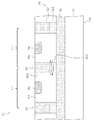
図3は、受光部11の構造の一例を示す模式図として、図2のX−Z面を切断面とする断面図を示す。図中には2つの光電変換素子111及びそれらの周辺領域を示す。受光部11は、公知の半導体製造プロセスを用いて半導体基板110に形成される。本実施形態では、半導体基板110は、比較的深い領域に形成された領域R1、領域R1上方(領域R1より浅い位置)に形成された領域R2、領域R2上方に形成された領域R3、領域3に形成された領域R4、及び、領域R3を区画する領域5を有する。尚、上記深い/浅いという表現は、半導体基板110の上面からの距離の大小関係を示し、以下の説明においても同様とする。
FIG. 3 is a schematic view showing an example of the structure of the
領域R1はN型であり、領域R1のN型不純物濃度は比較的低く設定されている。領域R2はN型であり、領域R2のN型不純物濃度は領域R1のものより高く設定されている。領域R3はN型であり、領域R3のN型不純物濃度は比較的低く(少なくとも領域R2のものより低く)設定されている。領域R4はP型であり、領域R4のP型不純物濃度は、不図示の配線部との電気接続がオーミック接触により実現されるように、比較的高く設定されている。また、領域R5はN型であり、領域R5のN型不純物濃度は、領域R3を電気的に分離して区画するように、領域R3のものより高く設定されている。 The region R1 is N-type, and the N-type impurity concentration of the region R1 is set to be relatively low. The region R2 is N-type, and the N-type impurity concentration of the region R2 is set higher than that of the region R1. The region R3 is N-type, and the N-type impurity concentration of the region R3 is set to be relatively low (at least lower than that of the region R2). The region R4 is P-type, and the P-type impurity concentration of the region R4 is set to be relatively high so that electrical connection with a wiring portion (not shown) is realized by ohmic contact. The region R5 is N-type, and the N-type impurity concentration of the region R5 is set higher than that of the region R3 so as to electrically separate and divide the region R3.
上記構造によれば、領域R3が領域R5で区画され且つ該区画された領域R3の個々に領域R4が形成されて、光電変換素子111が形成される。換言すると、領域R5は、互いに隣り合う光電変換素子111間の境界部に形成する。光電変換素子111としてのフォトダイオードは領域R3及びR4間のPN接合によって形成され、領域R3では入射光に応じて電荷(電子‐正孔対)が発生し、そのうちの小数キャリア(正孔)は領域R4に集められる。該小数キャリアは、その後、前述の読出部12により信号として読み出される。
According to the above structure, the region R3 is divided by the region R5, and the region R4 is formed in each of the divided regions R3 to form the
領域R3〜R5は、本実施形態ではエピタキシャル成長層に形成され、これにより、結晶性のよい半導体領域に光電変換素子111を形成可能となる。このエピタキシャル成長層は、例えば2μm以上、好適には4μm以上、かつ、例えば15μm以下、好適には10μm以下の厚さで形成される。本実施形態では、領域R3〜R5は、半導体基板110表面から0μm〜15μmの範囲内の深さに形成されているものとするが、0〜10μmの範囲内の深さに形成されてもよい。
In the present embodiment, the regions R3 to R5 are formed in the epitaxial growth layer, whereby the
ここで、図3に示されるように、領域R5は、半導体基板110表面付近の比較的浅い領域R51と、この領域R51より深く且つ領域R2より浅くに位置する領域R52とを含む。一般に、所定の導電型の半導体領域は、半導体基板110の上方から不純物注入を行うことで形成されるため、深い位置では浅い位置に比べて不純物濃度が低くなりうる。よって、詳細については後述とするが、上記領域R5においては、領域R52は、領域R51に比べてN型不純物濃度が低くなっている。
Here, as shown in FIG. 3, the region R5 includes a relatively shallow region R51 near the surface of the
上述の領域R1等の個々の導電型、及び、それらの不純物濃度の程度を見やすく表すと、
領域R1 N−
領域R2 N++
領域R3 N−
領域R4 P++
領域R51 N++
領域R52 N+
となる。尚、プラス(+、++)の記号は不純物濃度が比較的高いことを示し、マイナス(−)の記号は不純物濃度が比較的低いことを示す。
When the individual conductivity types such as the above-described region R1 and the degree of impurity concentration thereof are expressed in an easy-to-understand manner,
Region R1 N −
Region R2 N ++
Region R3 N −
Region R4 P ++
Region R51 N ++
Region R52 N +
It becomes. A plus (+, ++) sign indicates that the impurity concentration is relatively high, and a minus (−) sign indicates that the impurity concentration is relatively low.
まとめると、光電変換素子111は、P型(第1導電型)の領域R4(第1半導体領域)と、領域R4より深い位置に領域R4の底面を覆うように形成されたN型(第2導電型)の領域R3(第2半導体領域)と、領域R3より深い位置に形成され且つ領域R3よりもN型不純物濃度の高い領域R2(第3半導体領域)と、を含む。また、互いに隣り合う光電変換素子111の間には、それらの領域R3を電気的に分離するためのN型の領域R5(第4半導体領域)が形成されている。この領域R5は、領域R2よりも浅い位置に形成された領域R51(第1部分)と、領域R2よりも浅く且つ領域R51より深い位置に形成された領域R52と(第2部分)、を含む。領域R51のN型不純物濃度は領域R3より高く、また、領域R52のN型不純物濃度は領域R3より高く且つ領域R51より低い。
In summary, the
ここでは図3を参照しながら光電変換素子111の構造を述べたが、入射光が遮蔽されるように構成された光電変換素子112(図2参照)は、半導体基板110については上記光電変換部111同様の構造を有する。半導体基板110の上方には、配線層と絶縁層とが積層されて成る配線構造(不図示)が配され、光電変換素子112の直上には、この配線構造内に金属膜等の遮光性部材が設けられる。スケール2からの反射光は、この遮光性部材により遮蔽されることとなる。
Here, although the structure of the
図4(A)は、受光部11からの信号読出の態様を説明するための簡易回路図である。図1及び図2を参照しながら述べたとおり、受光部11は、複数の光電変換素子111及び112を含み、本実施形態では、それらの配列方向の最端に光電変換素子112が位置している。複数の光電変換素子111は選択部121により変換部122に選択的に接続され、ここでは説明の容易化のため、複数の光電変換素子111に対応して設けられた複数のスイッチ素子を選択部121として図示する。
FIG. 4A is a simplified circuit diagram for explaining a mode of signal reading from the
本明細書では、区別のため、オン状態(導通状態)のスイッチ素子に対応する光電変換素子111を「選択素子」と表現し、オフ状態(非導通状態)のスイッチ素子に対応する光電変換素子111を「非選択素子」と表現する。即ち、選択部121により選択された状態の光電変換素子111を選択素子とし、それ以外のものを非選択素子とする。
In this specification, for distinction, the
光電変換素子112は、本実施形態では、変換部122Xに接続されており、光電変換素子112の信号の経時的変化を取得可能とする。他の実施形態として、光電変換素子112は、光電変換素子111同様、スイッチ素子を介して変換部122Xに接続されてもよく、必要に応じて光電変換素子112の信号を読み出すこととしてもよい。図中において、光電変換素子112はストライプを付して示される。
In the present embodiment, the
図4(B)は、受光部11からの信号読出の態様の一例を図4(A)同様に示している。図中において、選択素子(オン状態のスイッチ素子に対応する光電変換素子)111は、ドットを付して示される。ここでは一例として、連続して並ぶ3つの選択素子1111〜1113、及び、それらから離間した位置において連続して並ぶ他の3つの選択素子1114〜1116から信号を読み出す態様が示される。このようにして、複数の光電変換素子111のうち任意のものが選択部121により選択的に変換部122に接続される。また、図中には、スケール2からの反射光の光量、即ち受光部11への入射光量、が比較的大きい領域として、領域R1(図1参照)が併せて示される。
FIG. 4B shows an example of a mode of signal reading from the
ところで、再び図3を参照すると、破線の矢印で示されるように、或る光電変換素子111の領域R3で生じた電荷は、N型不純物濃度が比較的低くなっている領域R52を通って、その隣の光電変換素子111の領域R3へ流出(漏出)する可能性がある。そのため、互いに隣り合う光電変換素子111間では、この電荷の流出に起因して、信号の干渉が発生することがある。このことは、例えば赤外光(波長780〜1000[nm]程度)等、比較的長波長の光が入射した場合、その光の半導体基板110への侵入深さは大きくなりうるため、顕著に表れうる。この現象は、クロストークとも称され、光源駆動部15が読出部12から受け取る信号に、このクロストークに起因する成分が混入することとなるため、前述のAPCの精度を低下させる原因ともなりうる。
By the way, referring to FIG. 3 again, as indicated by the dashed arrow, the charge generated in the region R3 of a certain
一例として、図4(B)において連続して並ぶ3つの選択素子1114〜1116のうち図中右側の1つ、即ち選択素子1116、に着目して述べる。選択素子1116は、図中において領域R1で示されるように比較的大きい光量の入射光を受けるが、それにより発生する電荷の一部は、選択素子1116の図中右隣に位置し且つ入射光量が比較的小さい非選択素子1117に流出してしまう可能性がある。そのため、選択素子1116から読出部12により読み出される信号値は、本来読み出されるべき信号値とは異なるものとなってしまう場合がある。
As an example, in out view of three selection elements 111 4-111 6 right one lined up successively in FIG. 4 (B), the words described by focusing on the
本実施形態では、図4(B)から分かるように、入射光が遮蔽される光電変換素子112は、入射光を受光可能な光電変換素子111(図中の1111)と隣り合っている。そのため、この光電変換素子111において入射光に応じて発生した電荷の一部は、光電変換素子112に流出する可能性がある。
In this embodiment, as can be seen from FIG. 4B, the
一方、光電変換素子112には光が実質的に入射しないため、光電変換素子112では熱ノイズ等に起因する電荷が発生しうる。この電荷に起因する電流は暗電流とも称される。この電荷量(或いは暗電流)は比較的小さいため、光電変換素子112から光電変換素子111への電荷の流出は、ここでは実質的にないものとする。
On the other hand, since light is not substantially incident on the
よって、光電変換素子112の信号は、光電変換素子112における暗電流に起因する電流成分(暗電流成分)に、光電変換素子111から光電変換素子112へ流出した電荷量に相当する成分(クロストーク成分)が重畳された形で、読出部12により読み出される。暗電流成分は比較的小さいため、光電変換素子112から読み出された信号は、実質的に、互いに隣り合う光電変換素子の一方から他方へのクロストーク成分に相当する、と言える。
Therefore, the signal of the
光源駆動部15は、この光電変換素子112から読み出された信号に基づいて、上記クロストークを考慮したAPCを行う。具体的には、光源駆動部15は、補正部152により参照信号VREF1を光電変換素子112の信号に基づいて補正し、加算部151の信号値が該補正された参照信号(VREF1’とする。)に近付くように、光源部16を駆動する。
The
換言すると、光源駆動部15は、上記補正済の参照信号VREF1’を、光源部16の発光光量が満たすべき目標値として、APCを行うこととなる。この観点において、補正部152は、参照信号VREF1と光電変換素子112の信号とに基づいて光源部16の発光光量の目標値を生成し、目標値生成部として機能している。
In other words, the light
加算部151の信号は、選択部121による複数の光電変換素子111の選択態様によって異なる。例えば、図4(B)の例では、連続して並ぶ3つの選択素子1114〜1116のうち、中央の選択素子1115については、その両隣の2つの選択素子1114及び1116への電荷の流出が考えられる一方で、それら選択素子1114及び1116からの電荷の流入も考えられる。これら3つの選択素子1114〜1116の信号は加算部151により加算される。そのため、上記中央の選択素子1115から得られる信号については、クロストークを考慮する必要は実質的にないと言える。
The signal of the
一方、選択素子1114及び1116については、それらの更に隣の非選択素子111との間で生じうる電荷の流出により本来読み出されるべき信号成分の一部が失われ、また、電荷の流入により本来読み出されるべきではない信号成分が混入しうる。即ち、これら2つの選択素子1114及び1116から得られる信号については、クロストークを考慮する必要があると言える。
On the other hand, the
よって、光源駆動部15は、選択素子111の信号値および光電変換素子112の信号値の他、更に、選択素子111と非選択素子111とが隣り合う箇所の数に基づいて、光源部16を駆動するとよい。即ち、上記補正済の参照信号VREF1’は、複数の光電変換素子111をどのような態様で選択しているかに基づいて、生成されうる。一例として、上記補正済の参照信号VREF1’は、
VREF1’=VREF1−(K×V112×N)
V112 :光電変換素子112の信号値(変換部122Xの出力値)
N :選択素子と非選択素子とが隣り合う箇所の数
K :係数
により生成可能である。
Therefore, the light
V REF1 ′ = V REF1 − (K × V 112 × N)
V 112 : Signal value of photoelectric conversion element 112 (output value of
N: Number of locations where the selected element and the non-selected element are adjacent. K: Can be generated by a coefficient.
上述のとおり、光電変換素子112の信号は、隣接素子111間の一方から他方へのクロストーク成分に相当するものとして、上記補正に用いられる。よって、上記補正の精度の向上のため、光電変換素子112は、光電変換素子111同様の構成(例えば上面レイアウト)で設けられるとよい。例えば、光電変換素子111及び112は、平面視において所定の対称性を形成するように設けられるとよく、好適には並進対称であるとよい。
As described above, the signal of the
また、上記クロストーク成分を光電変換素子112の信号に基づいて高い精度で特定可能とするため、光電変換素子111及び112が隣り合う面積を大きくしてもよい。即ち、光電変換素子111及び112は、平面視において、それぞれ長辺および短辺を有する矩形状となっており、それらの長辺において隣り合っているとよい。これにより、光電変換素子111から光電変換素子112への電荷の流出量が大きくなり、前述の暗電流成分に比べてクロストーク成分が支配的となるため、上記補正の精度を更に向上可能となる。
Further, in order to make it possible to specify the crosstalk component with high accuracy based on the signal of the
クロストーク量は入射光量に依存し、即ち、隣接素子111間の一方から他方への電荷の流出量は該一方への入射光量によって変動しうる。そのため、読出部12により光電変換素子112の信号の経時的変化を取得することで、補正部152は、その取得結果に基づく補正を行うことが可能となる。例えば、補正部152は、光電変換素子112の信号の積分値、最大値、平均値、中央値等に基づいて、参照信号VREF1を補正するとよい。本実施形態においては半導体装置1及びスケール2の相対移動により受光部11における光量分布がシフトするため、好適には、補正部152は、光電変換素子112の信号の積分値(所定期間における累積加算値)に基づいて参照信号VREF1を補正するとよい。
The amount of crosstalk depends on the amount of incident light, that is, the amount of charge flow from one side to the other between
他の実施形態として、補正部152は、参照信号VREF1を補正する代わりに、加算部151からの信号を補正してもよい。この場合、補正部152は、加算部151の信号と変換部122Xの信号とを受け取って該補正を行い、その結果を比較部153に出力する。比較部153は、補正部152からの信号と、参照信号VREF1(補正されていないもの)とを受け取り、それらを比較した結果に応じた電流を出力する。このような構成によってもAPCの精度を向上可能である。
As another embodiment, the correcting
付随的に、予め(例えばAPC開始前、製造時の検査工程等)、光電変換素子112及びその隣の光電変換素子111の信号を取得して、光電変換素子112の信号値を光電変換素子111の信号値と関連付けてもよい。即ち、入射光量とクロストーク量との相関関係(光電変換素子111の信号が何れの値の場合に光電変換素子112の信号が何れの値となるか)を示す情報を予め取得する。これにより上記補正を更に精度の高いものとすることも可能である。
In addition, the signal value of the
以上、本実施形態によれば、光源駆動部15は、光電変換素子111の信号および光電変換素子112の信号の双方に基づいて光源部16を駆動し、APCを行う。光電変換素子112の信号は、隣接素子111間の一方から他方へのクロストーク成分に相当するため、これを用いることで、APCの際には光源部16の発光光量の目標値を適切に設定可能となる。光源駆動部15は、加算部151の信号値がこの目標値に近付くように光源部16を制御することで、APCを高精度に行うことができる。
As described above, according to the present embodiment, the light
前述のとおり、クロストークは、例えば赤外光(波長780〜1000[nm]程度)等、比較的長波長の光が入射した場合に顕著に表れうる。そのため、本実施形態によれば、光源部16が赤色光を発生する構成において上記APCの精度を効果的に向上させることができる。尚、クロストークを抑制するため、例えば注入エネルギ及びドーズ量を大きくして深い不純物注入を追加的に行うことで領域R52の不純物濃度を高めることも可能であるが、本実施形態によれば、これを行うことなくAPCの精度を向上可能となる。よって、本実施形態によれば製造コストの低減にも有利であると言える。
As described above, crosstalk can be prominent when relatively long wavelength light such as infrared light (wavelength of about 780 to 1000 [nm]) is incident. Therefore, according to the present embodiment, the accuracy of the APC can be effectively improved in the configuration in which the
以上において実施形態およびそれに付随する幾つかの好適な例を示したが、本発明はこれらの例に限られるものではなく、本発明の趣旨を逸脱しない範囲で多様な変形ないし変更が可能である。 In the above, the embodiment and some suitable examples accompanying it have been described. However, the present invention is not limited to these examples, and various modifications or changes can be made without departing from the spirit of the present invention. .
例えば、本発明は、実施形態の反射型エンコーダの他、透過型エンコーダにも適用可能である。反射型エンコーダの場合、光源部16は、受光部11、読出部12、差動回路部13および光源駆動部15と共に共通の基材10上に配置され(図1及び図2参照)、それらは共通にパッケージングされる。一方、透過型エンコーダの場合、基材10とは異なる他の基材(第2基材)を用意し、光源部16は該他の基材に配置される。この場合、これら2つの基材は互いに向かい合うように配され、それらの間には、光源部16から受光部11への光を通過させる部分と、該光を遮蔽する部分とが交互に配された遮光用スケールが配されうる。
For example, the present invention can be applied to a transmissive encoder in addition to the reflective encoder of the embodiment. In the case of a reflective encoder, the
その他、実施形態では光学式エンコーダを例示したが、本発明は、所定の光源部を備える光源装置(例えばレーザ)、該光源部についてAPCを行う制御装置(例えばレーザドライバ)等、多様な電子機器に適用可能である。 In addition, although an optical encoder was illustrated in the embodiment, the present invention relates to various electronic devices such as a light source device (for example, a laser) including a predetermined light source unit, a control device for performing APC on the light source unit (for example, a laser driver) Applicable to
本明細書に記載された個々の用語は、本発明を説明する目的で用いられたものに過ぎず、本発明は、その用語の厳密な意味に限定されるものでないことは言うまでもなく、その均等物をも含みうる。 Each term used in this specification is merely used for the purpose of describing the present invention, and it is needless to say that the present invention is not limited to the strict meaning of the term. It can also contain things.
1:半導体装置、11:受光部、111及び112:光電変換素子、12:読出部、15:光源駆動部、16:光源部。 1: semiconductor device, 11: light receiving unit, 111 and 112: photoelectric conversion element, 12: reading unit, 15: light source driving unit, 16: light source unit.
Claims (17)
前記複数の光電変換素子の信号を読み出すための読出部と、
光源部を駆動するための光源駆動部と、を備え、
前記複数の光電変換素子は、
入射光を受光可能に構成された第1素子と、
入射光が遮蔽されるように構成された第2素子と、
を含んでおり、
前記光源駆動部は、前記読出部により読み出された前記第1素子の信号および前記第2素子の信号の双方に基づいて前記光源部を駆動する
ことを特徴とする半導体装置。 A plurality of photoelectric conversion elements arranged on a substrate;
A reading unit for reading signals of the plurality of photoelectric conversion elements;
A light source drive unit for driving the light source unit;
The plurality of photoelectric conversion elements are:
A first element configured to receive incident light;
A second element configured to shield incident light;
Contains
The semiconductor device according to claim 1, wherein the light source drive unit drives the light source unit based on both the signal of the first element and the signal of the second element read by the reading unit.
ことを特徴とする請求項1に記載の半導体装置。 The light source driving unit corrects a predetermined reference value based on the signal of the second element, and drives the light source unit so that the value of the signal of the first element approaches the corrected reference value. The semiconductor device according to claim 1.
ことを特徴とする請求項1または請求項2に記載の半導体装置。 The semiconductor device according to claim 1, wherein the second element is an endmost photoelectric conversion element in the arrangement direction of the plurality of photoelectric conversion elements.
前記光源部は、前記複数の光電変換素子、前記読出部および前記光源駆動部と共に共通の基材上に配置されている
ことを特徴とする請求項1から請求項3の何れか1項に記載の半導体装置。 Further comprising the light source unit,
The said light source part is arrange | positioned on a common base material with the said several photoelectric conversion element, the said read-out part, and the said light source drive part. It is any one of the Claims 1-3 characterized by the above-mentioned. Semiconductor device.
前記光源部が配置された第2基材と、を更に備え、
前記第1基材と前記第2基材とは、互いに向かい合うように配された
ことを特徴とする請求項1から請求項3の何れか1項に記載の半導体装置。 A first base material on which the plurality of photoelectric conversion elements, the reading unit, and the light source driving unit are disposed;
A second base material on which the light source unit is disposed,
The semiconductor device according to any one of claims 1 to 3, wherein the first base and the second base are arranged to face each other.
前記読出部は、前記第2素子の信号を読み出すと共に、前記複数の第1素子の一部を選択して該一部の信号を読み出し、
前記複数の第1素子のうち、前記選択されたものを選択素子とし、それ以外のものを非選択素子としたときに、
前記光源駆動部は、
前記第2素子の信号の値と、
前記選択素子からの信号の値と、
前記選択素子と前記非選択素子とが隣り合う箇所の数と、
に基づいて前記光源部を駆動する
ことを特徴とする請求項1から請求項5の何れか1項に記載の半導体装置。 The plurality of photoelectric conversion elements include a plurality of the first elements,
The reading unit reads a signal of the second element, selects a part of the plurality of first elements, and reads a part of the signal.
When the selected one of the plurality of first elements is a selection element and the other one is a non-selection element:
The light source driving unit is
The value of the signal of the second element;
The value of the signal from the selection element;
The number of locations where the selection element and the non-selection element are adjacent;
The said light source part is driven based on these. The semiconductor device in any one of the Claims 1-5 characterized by the above-mentioned.
ことを特徴とする請求項1から請求項6の何れか1項に記載の半導体装置。 7. The device according to claim 1, wherein the first element and the second element are provided so as to be adjacent to each other with symmetry in plan view. Semiconductor device.
ことを特徴とする請求項1から請求項7の何れか1項に記載の半導体装置。 In plan view, each of the plurality of photoelectric conversion elements is formed in a rectangular shape so as to have a long side and a short side, and the first element and the second element are at their long sides. The semiconductor device according to claim 1, wherein the semiconductor device is provided adjacent to each other.
ことを特徴とする請求項1から請求項8の何れか1項に記載の半導体装置。 The semiconductor device according to claim 1, wherein the light source unit generates infrared light.
前記基板は、
前記基板の断面において、前記第1半導体領域より深い位置に前記第1半導体領域の底面を覆うように形成された第2導電型の第2半導体領域と、
前記基板の断面において、前記第2半導体領域より深い位置に形成された前記第2導電型の第3半導体領域であって前記第2半導体領域よりも前記第2導電型の不純物濃度の高い第3半導体領域と、
を含む
ことを特徴とする請求項1から請求項9の何れか1項に記載の半導体装置。 Each of the plurality of photoelectric conversion elements includes a first semiconductor region of a first conductivity type formed on the substrate,
The substrate is
A second semiconductor region of a second conductivity type formed to cover the bottom surface of the first semiconductor region at a position deeper than the first semiconductor region in the cross section of the substrate;
A third semiconductor region of the second conductivity type formed at a position deeper than the second semiconductor region in the cross section of the substrate and having a higher impurity concentration of the second conductivity type than the second semiconductor region; A semiconductor region;
The semiconductor device according to any one of claims 1 to 9, further comprising:
ことを特徴とする請求項10に記載の半導体装置。 The semiconductor device according to claim 10, wherein the second semiconductor region is formed to a depth within a range of 0 μm to 15 μm from the surface of the substrate.
前記第4半導体領域は、
前記第3半導体領域よりも浅い位置に形成された前記第2導電型の第1部分であって前記第2半導体領域よりも前記第2導電型の不純物濃度の高い第1部分と、
前記第3半導体領域よりも浅く且つ前記第1部分より深い位置に形成された前記第2導電型の第2部分であって前記第2半導体領域よりも前記第2導電型の不純物濃度が高く且つ前記第1部分よりも前記第2導電型の不純物濃度が低い第2部分と、
を含む
ことを特徴とする請求項10または請求項11に記載の半導体装置。 In the cross section, the fourth semiconductor region of the second conductivity type is formed between the first semiconductor regions of the photoelectric conversion elements adjacent to each other,
The fourth semiconductor region is
A first portion of the second conductivity type formed at a position shallower than the third semiconductor region and having a higher impurity concentration of the second conductivity type than the second semiconductor region;
A second portion of the second conductivity type formed at a position shallower than the third semiconductor region and deeper than the first portion, wherein the impurity concentration of the second conductivity type is higher than that of the second semiconductor region; A second portion whose impurity concentration of the second conductivity type is lower than that of the first portion;
The semiconductor device according to claim 10, wherein the semiconductor device includes:
前記第2素子の信号は、前記光源駆動部および前記プロセッサのうち前記光源駆動部に出力される
ことを特徴とする請求項1から請求項12の何れか1項に記載の半導体装置。 The signal of the first element is output to the processor as a detection signal in addition to being output to the light source driver.
The semiconductor device according to any one of claims 1 to 12, wherein a signal of the second element is output to the light source drive unit among the light source drive unit and the processor.
ことを特徴とする請求項1から請求項13の何れか1項に記載の半導体装置。 The said 2nd element outputs the signal according to the light quantity of the incident light to the said 1st element located next to the said 2nd element. The statement in any one of Claims 1-13 characterized by the above-mentioned. The semiconductor device described.
前記光源駆動部は、前記複数の第1素子の信号を加算するための加算部を含む
ことを特徴とする請求項1から請求項14の何れか1項に記載の半導体装置。 The plurality of photoelectric conversion elements include a plurality of the first elements,
The semiconductor device according to any one of claims 1 to 14, wherein the light source drive unit includes an addition unit for adding signals of the plurality of first elements.
ことを特徴とする請求項1から請求項15の何れか1項に記載の半導体装置。 The light source driving unit drives the light source unit based on an integral value of the signal of the second element or a change with time of the signal of the second element. 2. A semiconductor device according to item 1.
ことを特徴とする光学式エンコーダ。 An optical encoder comprising the semiconductor device according to any one of claims 1 to 16.
Priority Applications (2)
| Application Number | Priority Date | Filing Date | Title |
|---|---|---|---|
| JP2018007590A JP7169745B2 (en) | 2018-01-19 | 2018-01-19 | Semiconductor devices and optical encoders |
| US16/237,891 US10788338B2 (en) | 2018-01-19 | 2019-01-02 | Semiconductor device and optical encoder comprising a light source driver to drive a light source based on signals from an incident light received first element and an incident light shielded second element |
Applications Claiming Priority (1)
| Application Number | Priority Date | Filing Date | Title |
|---|---|---|---|
| JP2018007590A JP7169745B2 (en) | 2018-01-19 | 2018-01-19 | Semiconductor devices and optical encoders |
Publications (2)
| Publication Number | Publication Date |
|---|---|
| JP2019128152A true JP2019128152A (en) | 2019-08-01 |
| JP7169745B2 JP7169745B2 (en) | 2022-11-11 |
Family
ID=67299237
Family Applications (1)
| Application Number | Title | Priority Date | Filing Date |
|---|---|---|---|
| JP2018007590A Active JP7169745B2 (en) | 2018-01-19 | 2018-01-19 | Semiconductor devices and optical encoders |
Country Status (2)
| Country | Link |
|---|---|
| US (1) | US10788338B2 (en) |
| JP (1) | JP7169745B2 (en) |
Citations (3)
| Publication number | Priority date | Publication date | Assignee | Title |
|---|---|---|---|---|
| JP2000311997A (en) * | 1999-02-25 | 2000-11-07 | Canon Inc | Photoelectric conversion device, image sensor and image input system provided with the same |
| JP2005265512A (en) * | 2004-03-17 | 2005-09-29 | Canon Inc | Optical encoder |
| JP2011154005A (en) * | 2010-01-28 | 2011-08-11 | Nikon Corp | Encoder |
Family Cites Families (3)
| Publication number | Priority date | Publication date | Assignee | Title |
|---|---|---|---|---|
| US8004724B2 (en) * | 2005-12-05 | 2011-08-23 | Canon Kabushiki Kaisha | Method and apparatus for image reading with synchronized readout and lighting control |
| JP2009031642A (en) | 2007-07-30 | 2009-02-12 | Canon Inc | Rocking body device, light deflector and image forming apparatus using it |
| JP2009031643A (en) | 2007-07-30 | 2009-02-12 | Canon Inc | Rocking body device, light deflector and image forming apparatus using it |
-
2018
- 2018-01-19 JP JP2018007590A patent/JP7169745B2/en active Active
-
2019
- 2019-01-02 US US16/237,891 patent/US10788338B2/en active Active
Patent Citations (3)
| Publication number | Priority date | Publication date | Assignee | Title |
|---|---|---|---|---|
| JP2000311997A (en) * | 1999-02-25 | 2000-11-07 | Canon Inc | Photoelectric conversion device, image sensor and image input system provided with the same |
| JP2005265512A (en) * | 2004-03-17 | 2005-09-29 | Canon Inc | Optical encoder |
| JP2011154005A (en) * | 2010-01-28 | 2011-08-11 | Nikon Corp | Encoder |
Also Published As
| Publication number | Publication date |
|---|---|
| US10788338B2 (en) | 2020-09-29 |
| US20190226884A1 (en) | 2019-07-25 |
| JP7169745B2 (en) | 2022-11-11 |
Similar Documents
| Publication | Publication Date | Title |
|---|---|---|
| US8264673B2 (en) | Back-illuminated distance measuring sensor and distance measuring device | |
| JP7039411B2 (en) | Photodetectors, photodetection systems, rider devices and cars | |
| JP5620087B2 (en) | Distance sensor and distance image sensor | |
| WO2020017180A1 (en) | Photodetection device, semiconductor photodetection element, and method for driving semiconductor photodetection element | |
| KR20140138625A (en) | Range sensor and range image sensor | |
| US20070210267A1 (en) | Optical ranging sensor and warm water wash toilet seat | |
| JP2009014461A (en) | Backside-illuminated distance measuring sensor and distance measuring device | |
| JP4971890B2 (en) | Back-illuminated distance measuring sensor and distance measuring device | |
| US10782428B1 (en) | Light receiving device and distance measuring apparatus | |
| JP2019128152A (en) | Semiconductor device and optical encoder | |
| JP2007232687A (en) | Optical range finder | |
| JP6862386B2 (en) | Photodetector, lidar device, and method of manufacturing photodetector | |
| JP2019057567A (en) | Photodetector, optical detection device, lidar device and manufacturing method of photodetector | |
| JP2021039066A (en) | Light detection device and electronic device | |
| EP4064350A1 (en) | Light detector | |
| JP2022169968A (en) | Photodetector, photodetection system, lidar device, and mobile object | |
| JP2021048207A (en) | Optical detector, optical detection system, rider device, and wheel | |
| JP7414776B2 (en) | Photodetectors, photodetection systems, lidar devices, and mobile objects | |
| US20220254945A1 (en) | Low-power photonic demodulator | |
| KR20140138618A (en) | Range sensor and range image sensor | |
| JP2012185174A (en) | Distance sensor and distance image sensor | |
| JP2004309387A (en) | Optical encoder | |
| US20190331773A1 (en) | Quadruple well for electrical cross-talk noise attenuation | |
| JP4372566B2 (en) | Photoelectric encoder | |
| JP2022107240A (en) | Photodetector, photodetection system, lidar device, mobile body, and vehicle |
Legal Events
| Date | Code | Title | Description |
|---|---|---|---|
| RD01 | Notification of change of attorney |
Free format text: JAPANESE INTERMEDIATE CODE: A7421 Effective date: 20210103 |
|
| A521 | Request for written amendment filed |
Free format text: JAPANESE INTERMEDIATE CODE: A523 Effective date: 20210113 |
|
| A621 | Written request for application examination |
Free format text: JAPANESE INTERMEDIATE CODE: A621 Effective date: 20210119 |
|
| A977 | Report on retrieval |
Free format text: JAPANESE INTERMEDIATE CODE: A971007 Effective date: 20211124 |
|
| A131 | Notification of reasons for refusal |
Free format text: JAPANESE INTERMEDIATE CODE: A131 Effective date: 20211220 |
|
| A521 | Request for written amendment filed |
Free format text: JAPANESE INTERMEDIATE CODE: A523 Effective date: 20220204 |
|
| A131 | Notification of reasons for refusal |
Free format text: JAPANESE INTERMEDIATE CODE: A131 Effective date: 20220701 |
|
| A521 | Request for written amendment filed |
Free format text: JAPANESE INTERMEDIATE CODE: A523 Effective date: 20220708 |
|
| TRDD | Decision of grant or rejection written | ||
| A01 | Written decision to grant a patent or to grant a registration (utility model) |
Free format text: JAPANESE INTERMEDIATE CODE: A01 Effective date: 20220930 |
|
| A61 | First payment of annual fees (during grant procedure) |
Free format text: JAPANESE INTERMEDIATE CODE: A61 Effective date: 20221031 |
|
| R151 | Written notification of patent or utility model registration |
Ref document number: 7169745 Country of ref document: JP Free format text: JAPANESE INTERMEDIATE CODE: R151 |