JP2019103100A - Signal generation device and signal generation method - Google Patents
Signal generation device and signal generation method Download PDFInfo
- Publication number
- JP2019103100A JP2019103100A JP2017235727A JP2017235727A JP2019103100A JP 2019103100 A JP2019103100 A JP 2019103100A JP 2017235727 A JP2017235727 A JP 2017235727A JP 2017235727 A JP2017235727 A JP 2017235727A JP 2019103100 A JP2019103100 A JP 2019103100A
- Authority
- JP
- Japan
- Prior art keywords
- signal
- output
- signal generation
- difference
- comparison
- Prior art date
- Legal status (The legal status is an assumption and is not a legal conclusion. Google has not performed a legal analysis and makes no representation as to the accuracy of the status listed.)
- Granted
Links
Images


Abstract
Description
本発明は、信号生成装置、及び信号生成方法に関し、特に増幅器を含む信号生成装置、及び信号生成方法に関する。 The present invention relates to a signal generation device and a signal generation method, and more particularly to a signal generation device including an amplifier and a signal generation method.
無線システムの送信機は、低消費電力で動作することが望ましい。特に、送信機の最終段の信号増幅器は、送信機全体の50%以上の電力を消費する。よって、最終段の信号増幅器の電力効率を上げることが求められる。最終段に用いられうる信号増幅器として、スイッチング増幅器を用いるものが知られている。 It is desirable for the transmitter of the wireless system to operate with low power consumption. In particular, the signal amplifier at the final stage of the transmitter consumes 50% or more of the power of the entire transmitter. Therefore, it is required to increase the power efficiency of the final stage signal amplifier. As a signal amplifier that can be used for the final stage, one using a switching amplifier is known.
スイッチング増幅器の電力損失は、スイッチングロスにより生じるものの寄与が大きい。そのため、出力信号に影響を与えずスイッチング回数を削減する変調方法が重要となる。 The power loss of the switching amplifier is largely due to the switching loss. Therefore, a modulation method that reduces the number of switchings without affecting the output signal is important.
最小となるパルス幅を制限しスイッチング回数の削減を可能とするデルタシグマ変調回路、及びそれを制御信号としてスイッチング増幅器を用いて信号の増幅を行うことに関しては、例えば特許文献1の背景技術として提案されている。
With regard to a delta sigma modulation circuit that limits the minimum pulse width and enables reduction of switching times, and performing signal amplification using the switching amplifier as the control signal, for example, proposed as a background art of
また、スイッチング増幅器を電源変調器として用いたエンベロープトラッキング方式の増幅器に関しては、例えば特許文献2で提案されている。
An envelope tracking type amplifier using a switching amplifier as a power supply modulator is proposed in, for example,
上述の特許文献1、特許文献2の増幅器は電力効率が高いことが知られているが、それでも無線送信機に求められる電力効率を達成することは難しい。またそれらを組み合わせたもの、すなわち、入力信号の包絡線成分の最小パルス幅を制限してデルタシグマ変調し、更にスイッチング増幅器で増幅したものを電源変調信号として用いる増幅器であっても、改善はあるものの同様である。
Although it is known that the amplifiers of
スイッチング素子を用いた増幅器において、その電力効率の低下の大きな原因の一つはスイッチングの際に生じる電力損失である。電力効率向上のためにはこのスイッチングロスを抑える必要がある。即ち、単位時間あたりのスイッチング回数を抑える必要がある。 In an amplifier using a switching element, one of the major causes of the reduction in power efficiency is the power loss that occurs during switching. In order to improve power efficiency, it is necessary to suppress this switching loss. That is, it is necessary to suppress the number of switchings per unit time.
しかし、一方でスイッチング回数を抑えることは信号の自由度を制限することになり、アナログデジタル変換の際には信号対雑音比を悪化させることにつながる。 However, on the other hand, reducing the number of times of switching limits the degree of freedom of the signal and leads to deterioration of the signal-to-noise ratio in analog-to-digital conversion.
アナログ信号をデジタル変調しスイッチング増幅器で増幅する際に、所望信号近傍の量子化雑音を抑えつつ、スイッチング回数を既存方式よりも更に低減するための変調方式が課題となっている。 When an analog signal is digitally modulated and amplified by a switching amplifier, a modulation scheme for further reducing the number of times of switching compared to the existing scheme while suppressing quantization noise in the vicinity of a desired signal has become an issue.
特許文献3や特許文献5では、デルタシグマ変調回路を含んだスイッチング電源が提案され、特許文献4では、デルタシグマ変調回路を含んだスイッチング回路が提案されている。
本発明の目的は、スイッチング回数を低減しつつ、信号対雑音比の高い信号を生成する信号生成装置、及び信号生成方法を提供することにある。 An object of the present invention is to provide a signal generation device and a signal generation method that generate a signal with a high signal-to-noise ratio while reducing the number of switching times.
前記目的を達成するため、本発明に係る信号生成装置は、出力信号を遅延させる遅延手段と、入力信号と上記遅延手段からの信号との差分を取る差分手段と、加算手段と、上記加算手段からの出力を積分する積分手段と、上記積分手段からの出力を離散化して上記出力信号を生成する比較手段と、上記比較手段からの上記出力信号の変化状態を示す信号を上記加算手段に供給して、上記加算手段で上記差分手段からの信号と上記加算手段で加算させる帰還手段と、を含む。 In order to achieve the above object, a signal generation apparatus according to the present invention comprises: delay means for delaying an output signal; difference means for taking a difference between an input signal and a signal from the delay means; addition means; Integrating means for integrating the output from the above, comparing means for discretizing the output from the integrating means to generate the output signal, and supplying the signal indicating the change state of the output signal from the comparing means to the adding means And feedback means for causing the addition means to add the signal from the difference means in the addition means.
発明に係る信号生成方法は、遅延手段、差分手段、加算手段、積分手段、比較手段、及び帰還手段を含む信号生成装置の信号生成方法であって、
上記遅延手段が、出力信号を遅延させ、
上記差分手段が、上記入力信号と上記遅延手段からの信号との差分を取り、
上記積分手段が、上記加算手段からの出力を積分し、
上記比較手段が、上記積分手段からの出力を離散化して上記出力信号を生成し、
上記帰還手段が、上記比較手段からの上記出力信号の変化状態を示す信号を上記加算手段に供給して、上記差分手段からの信号と上記加算手段で加算させる。
A signal generation method according to the invention is a signal generation method of a signal generation device including delay means, difference means, addition means, integration means, comparison means, and feedback means,
The delay means delays the output signal,
The difference means takes the difference between the input signal and the signal from the delay means;
The integrating means integrates the output from the adding means;
The comparing means discretizing the output from the integrating means to generate the output signal;
The feedback means supplies a signal indicating the change state of the output signal from the comparison means to the addition means, and causes the addition means to add the signal from the difference means.
本発明によれば、スイッチング回数を低減しつつ、信号対雑音比の高い信号を生成する信号生成装置、及び信号生成方法を提供できる。 According to the present invention, it is possible to provide a signal generation device and a signal generation method that generate a signal with a high signal-to-noise ratio while reducing the number of switching times.
本発明の好ましい実施形態について、図面を参照しながら詳細に説明する。具体的な実施形態について説明する前に、本発明の上位概念による実施形態の信号生成装置について説明する。 Preferred embodiments of the present invention will be described in detail with reference to the drawings. Before describing a specific embodiment, a signal generation apparatus according to a high-level embodiment of the present invention will be described.
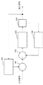
図1は、上位概念による実施形態の信号生成装置を説明するためのブロック図である。図1の信号生成装置は、差分手段101、加算手段102、積分手段103、比較手段104、遅延手段105、及び帰還手段106を含む。 FIG. 1 is a block diagram for explaining a signal generating apparatus according to a high-level concept embodiment. The signal generation apparatus of FIG. 1 includes difference means 101, addition means 102, integration means 103, comparison means 104, delay means 105, and feedback means 106.
図1の信号生成装置において、差分手段101は入力信号と遅延手段105の出力信号の差を出力する。加算手段102は、差分手段101の出力と帰還手段106の出力信号の和を出力する。積分手段103は、加算手段102の出力信号を積分する。比較手段104は、積分手段103から出力される信号を基準値と比較することによって、信号をデジタル化する。デジタル化された信号は、信号生成装置の出力信号になると共に、遅延手段105に入力される。また比較手段104の出力信号の変化状態を示す信号が、帰還手段106に入力される。
In the signal generation apparatus of FIG. 1, the difference means 101 outputs the difference between the input signal and the output signal of the delay means 105. The addition means 102 outputs the sum of the output of the difference means 101 and the output signal of the feedback means 106. The integrating means 103 integrates the output signal of the adding
図1の信号生成装置では、積分手段103から出力される信号を基準値と比較する比較手段104は、比較手段104の出力信号の変化状態を示す信号を出力する。この比較手段104の出力信号の変化状態を示す信号を用い、帰還手段106を経由し、加算手段102で差分手段101の出力と加算している。比較手段104の端子からの出力は積分手段103に対し、比較手段104の出力が変化した際に、積分手段103の積分値と変化の引き金となった比較手段104の内部基準値の絶対値が大きくなるように作用する。これによりパルス幅が広くなり、スイッチング回数は減少する。結果として出力信号の単位時間あたりのスイッチング回数が少なくなる。
In the signal generation apparatus of FIG. 1, the comparison means 104 which compares the signal output from the integration means 103 with the reference value outputs a signal indicating the change state of the output signal of the comparison means 104. The signal indicating the change state of the output signal of the comparison means 104 is added to the output of the difference means 101 by the addition means 102 via the feedback means 106. The output from the terminal of the
このスイッチング回数を削減できたことによって、信号生成装置の電力効率を改善することができる。以下、より具体的な実施形態について図面を参照しながら説明する。 By reducing the number of times of switching, the power efficiency of the signal generator can be improved. Hereinafter, more specific embodiments will be described with reference to the drawings.
〔第1実施形態〕
第1実施形態の信号生成装置について、説明する。
First Embodiment
The signal generation device of the first embodiment will be described.
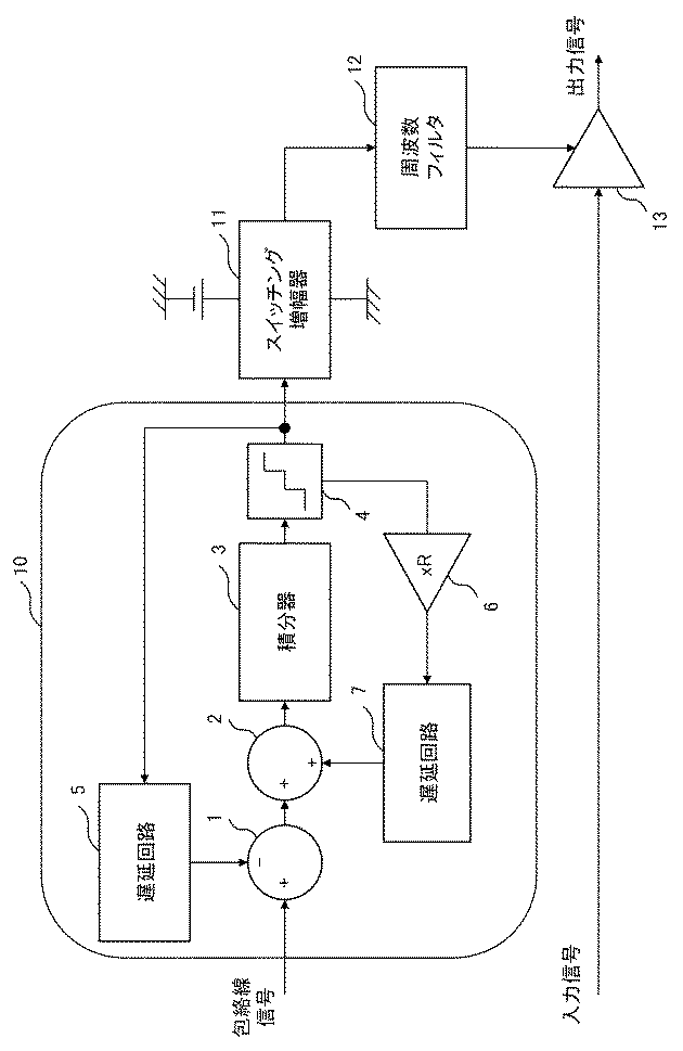
図2は、第1実施形態の信号生成装置を説明するためのブロック図である。図2に示す信号生成装置は、差分器1、加算器2、積分器3、比較器4、遅延回路5、増幅器6、及び遅延回路7を含む。
FIG. 2 is a block diagram for explaining the signal generation device of the first embodiment. The signal generation device shown in FIG. 2 includes a
図2の信号生成装置において、差分器1はアナログ入力信号と遅延回路5の出力信号との差分を取り、この差分を出力する。加算器2は、差分器1の出力と遅延回路7の出力信号の和を出力する。積分器3は、加算器2の出力信号を積分する。比較器4は、積分器3からの出力を離散化する。言い換えると比較器4は、積分器3から出力される信号を基準値と比較することによって、信号をデジタル化する。デジタル化された信号は、信号生成装置の出力信号になると共に、遅延回路5に入力される。遅延回路5は入力された信号を遅延して差分器1に供給する。
In the signal generation device of FIG. 2, the
比較器4は、信号生成装置の出力信号を出力する出力端子以外に、その出力信号の変化状態を示す信号を外部に出力する端子を持つ。以下では、比較器4の出力信号の変化状態を示す信号を外部に出力する端子を、比較器4の変化出力端子と称することがある。この変化状態を示す信号を外部に出力する端子は例えば、比較器4の出力信号がより小さい方向に変化した際には−1を、比較器4の出力信号がより大きい方向に変化した際には1を、それ以外の場合には0を出力する。この比較器4の出力信号の変化状態を示す信号は増幅器6に入力されて、増幅器6でR倍に増幅される。ここで、Rは正の実数とする。増幅器6の出力は、遅延回路7に入力される。遅延回路7は、入力された信号を遅延して加算器2に供給する。
The comparator 4 has, in addition to the output terminal for outputting the output signal of the signal generation device, a terminal for outputting a signal indicating the change state of the output signal to the outside. Below, the terminal which outputs the signal which shows the change state of the output signal of the comparator 4 outside may be called the change output terminal of the comparator 4. FIG. For example, when the output signal of the comparator 4 changes in a smaller direction, the terminal that outputs the signal indicating this change state to the outside, or when the output signal of the comparator 4 changes in a larger direction. Will
図3は、図2の信号生成装置の信号を示す波形図である。図3は、信号生成装置へのアナログ入力信号として定数を入力している状態で、比較器4の出力レベルが2値の場合の、積分器3の出力A、比較器4の変化出力端子からの変化出力B、及び比較器4の出力Cを示したものである。
FIG. 3 is a waveform diagram showing signals of the signal generator of FIG. FIG. 3 shows that the output A of the
比較器4の変化出力端子からの出力は積分器3に対し、比較器4の出力が変化した際に、積分器3の積分値と変化の引き金となった比較器4の内部基準値の絶対値が大きくなるように作用する。例えば、具体的には比較器4の内部基準値が0の場合、比較器4の出力が負から正に変化した場合にはRが、正から負に変化した場合には−Rが加算器2を経て積分器3の入力に加算されることとなる。
The output from the change output terminal of the comparator 4 is the absolute value of the integral value of the
この作用の程度は、増幅器6の増幅率Rによって決まる。具体的には、増幅率Rが大きいほど、積分器3の出力が再度変化の引き金となった比較基準値に到達するまでの時間が長くなる。つまり、パルス幅が広くなる。また、増幅率Rが0の場合はパルス幅制限されていない既存のデルタシグマ変調と同じになり、最小パルス幅は1となる。図3の場合は、増幅率Rの効果により、最小パルス幅が5になっている。このパルス幅が長くなることにより、スイッチング回数は減少する。結果として、信号生成装置の出力信号の単位時間あたりのスイッチング回数が少なくなる。このスイッチング回数を削減できたことによって、図3の信号生成装置では電力効率の改善を実現できる。
The extent of this effect depends on the amplification factor R of the
図3の信号生成装置では、比較器4の出力が積分器3へと常に帰還される構成になっている。これにより、図3の信号生成装置ではより適切にデルタシグマ変調のフィードバックが働くので、よりスイッチング回数を削減することが可能となる。
In the signal generating device of FIG. 3, the output of the comparator 4 is always fed back to the
[効果の説明]
第1実施形態の信号生成装置を用いることで、スイッチング回数を抑えつつアナログ信号からデルタシグマ変調したデジタル信号を得ることができる。
[Description of effect]
By using the signal generation device according to the first embodiment, it is possible to obtain a digital signal that has been subjected to delta sigma modulation from an analog signal while suppressing the number of times of switching.
〔第2実施形態〕
次に、第2実施形態の信号生成装置について、説明する。本発明の信号生成装置は、上述した第1実施形態の構成に限られるものではなく、様々な変形や追加などが可能である。第2実施形態の信号生成装置は、第2実施形態の信号生成装置の変形例である。
Second Embodiment
Next, the signal generation device of the second embodiment will be described. The signal generation apparatus of the present invention is not limited to the configuration of the first embodiment described above, and various modifications, additions, and the like are possible. The signal generation device of the second embodiment is a modification of the signal generation device of the second embodiment.
図4は、第2実施形態の信号生成装置を説明するためのブロック図である。第1実施形態の信号生成装置と同様な構成に対しては、同じ参照番号を付すことにより、その詳細な説明を省略することとする。 FIG. 4 is a block diagram for explaining a signal generation device of the second embodiment. The same components as those of the signal generating apparatus according to the first embodiment are designated by the same reference numerals, and the detailed description thereof will be omitted.
図4の信号生成装置は、図2の信号生成装置と同様に、差分器1、加算器2、積分器3、比較器4、遅延回路5、及び増幅器6を含む。さらに図4の信号生成装置は、デジタルフィルタ8を含む。図4のデジタルフィルタ8は、比較器4の出力信号、すなわち信号生成装置の出力信号を入力して増幅器6へ出力する。そして図4の増幅器6は、R倍に増幅した後、加算器2に供給する。
The signal generation device of FIG. 4 includes a
ここでデジタルフィルタ8の伝達関数は例えば、
Here, the transfer function of the
とする。これにより図4の加算器2へ、図2に示される第1実施形態の信号生成装置と同じ信号が供給されるよう、構成する。ここで、nは比較器4が出力するレベルの数、xkは比較器4の下から数えてk番目の出力レベルである。このような伝達関数により、図4のデジタルフィルタ8は、比較器4の出力信号がより小さい方向に変化した際には−1を、比較器4の出力信号がより大きい方向に変化した際には1を、それ以外の場合には0を出力する。
I assume. As a result, the
図4の信号生成装置では、比較器4の出力信号をデジタルフィルタ8に入力することで、第1実施形態の比較器4における出力信号の変化を外部に出力する端子(変化出力端子)からの出力を遅延させたものと同じ信号を得ることができる。よって、図4の信号生成装置の出力信号は、第1実施形態のものと同じものとなる。
In the signal generation device of FIG. 4, the output signal of the comparator 4 is input to the
[効果の説明]
これにより、第1実施形態の信号生成装置とは一部異なる構成を採用しつつ、第1実施形態の信号生成装置と同等の効果を得ることができる。
[Description of effect]
Thereby, the same effect as that of the signal generation device of the first embodiment can be obtained while adopting a configuration that is partially different from the signal generation device of the first embodiment.
すなわち、第1実施形態の信号生成装置と同様に、増幅器6の増幅率Rが大きいほど、積分器3の出力が再度変化の引き金となった比較基準値に到達するまでの時間が長くなり、パルス幅が広くなる。また、増幅器6の増幅率Rが0の場合はパルス幅制限されていない既存のデルタシグマ変調と同じになり、最小パルス幅は1となる。増幅器6の増幅率Rの効果により、最小パルス幅が長くなり、スイッチング回数は減少する。結果として、信号生成装置の出力信号の単位時間あたりのスイッチング回数が少なくなる。このスイッチング回数を削減できたことによって、図4の信号生成装置においても電力効率の改善を実現できる。
That is, as in the signal generation device of the first embodiment, as the amplification factor R of the
〔第3実施形態〕
次に、第3実施形態の信号生成装置について、説明する。本実施形態は、第1実施形態の信号生成装置を含んで信号生成装置を構成したものである。図5は、第3実施形態の信号生成装置を説明するためのブロック図である。第1実施形態の信号生成装置と同様な構成に対しては、同じ参照番号を付すことにより、その詳細な説明を省略することとする。
Third Embodiment
Next, a signal generation device according to a third embodiment will be described. In the present embodiment, the signal generation device is configured to include the signal generation device of the first embodiment. FIG. 5 is a block diagram for explaining a signal generation device of the third embodiment. The same components as those of the signal generating apparatus according to the first embodiment are designated by the same reference numerals, and the detailed description thereof will be omitted.
図5の信号生成装置は、デルタシグマ変調部10、スイッチング増幅器11、及び周波数フィルタ12を含む。図5の信号生成装置のデルタシグマ変調部10は、第1実施形態として説明した図2の信号生成装置と同じ構成を採用したものである。なお、前述の通り、第2実施形態として説明した図4の信号生成装置は第1実施形態の信号生成装置と等価な出力信号を得られるので、図5の信号生成装置のデルタシグマ変調部10として、図4の信号生成装置を用いてもよい。
The signal generation device of FIG. 5 includes a delta
図5の信号生成装置の入力信号としてのアナログ入力信号は、デルタシグマ変調部10によりデジタル信号に変換される。得られたデジタル信号は、スイッチング増幅器11に入力され、増幅される。スイッチング増幅器11からの出力は、周波数フィルタ12に入力される。周波数フィルタ12によって所望周波数帯域のみが切り出され、出力信号として出力される。
[効果の説明]
スイッチング増幅器の電力損失の大部分は、出力値の変化の際に生じるスイッチングロスによって生じる。スイッチングロスは、スイッチング増幅器の単位時間あたりのスイッチング回数に比例する。
An analog input signal as an input signal of the signal generation apparatus of FIG. 5 is converted into a digital signal by the delta
[Description of effect]
Most of the power loss of the switching amplifier is caused by the switching loss that occurs when the output value changes. The switching loss is proportional to the number of switchings per unit time of the switching amplifier.
本実施形態の信号生成装置では、第1実施形態の信号生成装置を用いて入力信号をデルタシグマ変換することにより、信号対雑音比を保ったまま、スイッチング回数を低減させたデジタル信号を得ることができる。このデジタル信号をスイッチング増幅器の入力として用いることで、スイッチング増幅器のスイッチングロスを低減することができ、電力効率を改善することができる。 In the signal generation device of the present embodiment, the input signal is subjected to delta sigma conversion using the signal generation device of the first embodiment to obtain a digital signal in which the number of times of switching is reduced while maintaining the signal to noise ratio. Can. By using this digital signal as the input of the switching amplifier, the switching loss of the switching amplifier can be reduced and the power efficiency can be improved.
〔第4実施形態〕
次に、第4実施形態の信号生成装置について、説明する。本実施形態は、第3実施形態の信号生成装置の変形例であり、第3実施形態の信号生成装置と同様に、第1実施形態の信号生成装置を含んで信号生成装置を構成したものである。図6は、第4実施形態の信号生成装置を説明するためのブロック図である。第1実施形態の信号生成装置や第3実施形態の信号生成装置と同様な構成に対しては、同じ参照番号を付すことにより、その詳細な説明を省略することとする。
Fourth Embodiment
Next, a signal generation device of a fourth embodiment will be described. The present embodiment is a modification of the signal generation device of the third embodiment, and the signal generation device is configured to include the signal generation device of the first embodiment as in the signal generation device of the third embodiment. is there. FIG. 6 is a block diagram for explaining a signal generation device of the fourth embodiment. The same components as those of the signal generation device of the first embodiment and the signal generation device of the third embodiment are denoted by the same reference numerals, and the detailed description thereof is omitted.
図6の信号生成装置は、第3実施形態の信号生成装置と同様に、デルタシグマ変調部10、スイッチング増幅器11、及び周波数フィルタ12を含む。さらに図6の信号生成装置は、入力信号を増幅して出力する増幅器13を含む。
The signal generation apparatus of FIG. 6 includes a delta
図6の信号生成装置では、入力信号が増幅器13により増幅され、出力信号として出力される。また、デルタシグマ変調部10への入力は、入力信号の包絡線信号となっている。周波数フィルタからの出力は増幅器13へ変調電源として入力される。図6の信号生成装置では、包絡線信号がデルタシグマ変調部10に入力され、デルタシグマ変調部10によりデジタル信号に変換される。さらに、第3実施形態と同様に、得られたデジタル信号はスイッチング増幅器11に入力され、増幅される。スイッチング増幅器11からの出力は、周波数フィルタ12に入力される。周波数フィルタ12によって所望周波数帯域のみが切り出され、出力信号として出力される。そして本実施形態では、周波数フィルタ12の出力が増幅器13の電源として用いられる。
In the signal generator of FIG. 6, the input signal is amplified by the
[効果の説明]
本実施形態の信号生成装置では、第3実施形態の信号生成装置と同様に、第1実施形態の信号生成装置を用いて入力信号をデルタシグマ変換することにより、信号対雑音比を保ったまま、スイッチング回数を低減させたデジタル信号を得ることができる。このデジタル信号をスイッチング増幅器の入力として用いることで、スイッチング増幅器のスイッチングロスを低減することができ、電力効率を改善することができる。
[Description of effect]
Similar to the signal generation device of the third embodiment, the signal generation device of the present embodiment delta sigma converts the input signal using the signal generation device of the first embodiment while maintaining the signal to noise ratio. Digital signals with reduced number of switching can be obtained. By using this digital signal as the input of the switching amplifier, the switching loss of the switching amplifier can be reduced and the power efficiency can be improved.
さらに本実施形態の信号生成装置では、第3実施形態の信号生成装置を増幅器13の電源変調器として用いることで、電力効率の高い増幅器を提供することができる。
Furthermore, in the signal generation device of the present embodiment, by using the signal generation device of the third embodiment as a power supply modulator of the
〔第5実施形態〕
上述した第1実施形態や第2実施形態などのさらなる変形例として、第5実施形態の信号生成装置を説明する。図7は第5実施形態の信号生成装置を説明するためのブロック図である。第1実施形態の信号生成装置と同様な構成に対しては、同じ参照番号を付すことにより、その詳細な説明を省略することとする。
Fifth Embodiment
The signal generation apparatus of the fifth embodiment will be described as a further modification of the first embodiment, the second embodiment, and the like described above. FIG. 7 is a block diagram for explaining a signal generation device of the fifth embodiment. The same components as those of the signal generating apparatus according to the first embodiment are designated by the same reference numerals, and the detailed description thereof will be omitted.
図7の信号生成装置は、第1実施形態の信号生成装置と同様に、差分器1、積分器3、及び遅延回路5を含む。図7の信号生成装置では、第1実施形態の信号生成装置と比較すると、増幅器6と遅延回路7がなくなっている。また、比較器4が幅Rのヒステリシスを持つ比較器9に置き換えられている。
The signal generation device of FIG. 7 includes a
図8は、図7の信号生成装置の信号を示す波形図である。図8は、信号生成装置へのアナログ入力信号として定数を入力している状態で、比較器9の出力レベルが−1と1の2値の場合の、積分器3の出力A、及び比較器9の出力と比較器9の基準値を示したものである。
FIG. 8 is a waveform diagram showing signals of the signal generation device of FIG. FIG. 8 shows the output A of the
積分器3からの出力が比較器9の基準値をまたぐと、比較器9のヒステリシス効果により比較器9の基準値は幅Rだけ比較器9の入力値から離れる方向に変化する。これは、比較器9の基準値を固定して考えた場合に、積分器3の出力値が幅Rだけ比較器9の基準値から離れる方向に変化することを意味する。したがって、比較器9からの出力は、第1実施形態の比較器4からの出力と同じものとなる。
When the output from the
また、ヒステリシスの幅Rを比較器9の出力レベルの差よりも大きく取ることで、比較器の出力パルス幅の最小値をヒステリシスがない場合に比べてより大きくすることができる。
Further, by setting the width R of the hysteresis larger than the difference between the output levels of the
[効果の説明]
本実施形態の信号生成装置では、第1実施形態の信号生成装置よりも簡易な構成としつつ、第1実施形態の信号生成装置と同等の電力効率の改善効果が期待される。
[Description of effect]
The signal generation device of the present embodiment is expected to have the same effect of improving the power efficiency as the signal generation device of the first embodiment while having a simpler configuration than the signal generation device of the first embodiment.
〔その他の実施形態〕
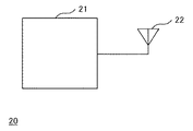
上述した第1乃至第5実施形態の信号生成装置を含んで、無線送信機を構成することができる。図11は、その他の実施形態の無線送信機を示す概略図である。図11の無線送信機20は、無線信号を生成する信号生成装置21と、信号生成装置21で生成された無線信号を送信するアンテナ22と、を含む。
Other Embodiments
A wireless transmitter can be configured including the signal generation devices of the first to fifth embodiments described above. FIG. 11 is a schematic view showing a wireless transmitter of another embodiment. The
第1乃至第5実施形態の信号生成装置を、このような無線送信機の最終段増幅器に用いて無線送信機を構成することができる。この無線送信機は、第1乃至第5実施形態の信号生成装置を用いたことにより、電力効率を向上させることができる。 The signal generation apparatus of the first to fifth embodiments can be used as a final stage amplifier of such a wireless transmitter to configure a wireless transmitter. This wireless transmitter can improve power efficiency by using the signal generation devices of the first to fifth embodiments.
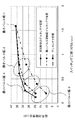
図9は、第1実施形態の信号生成装置と背景技術のデルタシグマ変調方式について、245.76Mbpsサンプリングの帯域20MHz LTE信号の包絡線信号を入力した際の、単位時間当たりのスイッチング回数に対する信号対雑音比(直流成分を除く)を数値計算した結果を示すグラフである。
FIG. 9 is a signal pair with respect to the number of switching times per unit time when an envelope signal of a
図9では、第1実施形態による出力信号(実施形態のデルタシグマ変調)、特許文献1の図5のような回路方式による出力信号(最小パルス幅制限デルタシグマ変調)、及び一般的なデルタシグマ変調(デルタシグマ変調)について、最小パルス幅が1、2、4、8の場合をプロットしている。なお、オーバーサンプリングレートは8とした。最小パルス幅が1の場合、どの方式も同じ信号を生成する。 In FIG. 9, the output signal according to the first embodiment (delta sigma modulation of the embodiment), the output signal according to the circuit system as shown in FIG. 5 of Patent Document 1 (minimum pulse width limited delta sigma modulation), and general delta sigma The case where the minimum pulse width is 1, 2, 4 and 8 is plotted for modulation (delta sigma modulation). The oversampling rate is eight. If the minimum pulse width is one, then any scheme produces the same signal.
計算の結果、第1実施形態の方式では、得られる信号対雑音比を固定してみた場合、より少ないスイッチング回数の信号を生成できることがわかった。また、最小パルス幅を固定してみた場合でも、より少ないスイッチング回数でより信号対雑音比が高い信号を得ることができることがわかった。 As a result of the calculation, it was found that in the method of the first embodiment, when the obtained signal-to-noise ratio is fixed, it is possible to generate a signal with a smaller number of switching times. It was also found that even when the minimum pulse width was fixed, it was possible to obtain a signal with a higher signal-to-noise ratio with a smaller number of switchings.
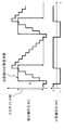
図10は、第1実施形態による出力信号(実施形態のデルタシグマ変調)と、特許文献1の図5のような回路方式による出力信号(最小パルス幅制限デルタシグマ変調)とについて、パルス幅の出現回数の分布を数値計算した結果を示している。パルス幅の最小値は、共に8とした。 FIG. 10 shows pulse widths of the output signal according to the first embodiment (delta sigma modulation of the embodiment) and the output signal according to the circuit system as shown in FIG. 5 of patent document 1 (minimum pulse width limited delta sigma modulation). It shows the results of numerical calculation of the distribution of the number of occurrences. The minimum value of the pulse width was 8 in both cases.
計算の結果、第1実施形態の方式は特許文献1の図5のような回路方式による出力信号(最小パルス幅制限デルタシグマ変調)に比べ、より幅の広いパルスが多く分布していることがわかった。背景技術の方式に比べパルス幅の広い信号をより多く出力するので、時間応答性の悪いデバイスを用いた場合であっても性能劣化を起こしにくいことがわかった。 As a result of calculation, in the method of the first embodiment, a wider number of wider pulses are distributed as compared with the output signal (minimum pulse width limited delta sigma modulation) according to the circuit method as shown in FIG. all right. As more signals with wider pulse widths are output as compared with the method of the background art, it has been found that performance degradation is less likely to occur even when using devices with poor time response.
以上、本発明の好ましい実施形態や実施例を説明したが、本発明はこれに限定されるものではない。特許請求の範囲に記載した発明の範囲内で、種々の変形が可能であり、それらも本発明の範囲に含まれることはいうまでもない。 Although the preferred embodiments and examples of the present invention have been described above, the present invention is not limited thereto. It is needless to say that various modifications are possible within the scope of the invention described in the claims, and they are also included in the scope of the present invention.
上記の実施形態の一部又は全部は、以下の付記のようにも記載されうるが、以下には限られない。
(付記1)出力信号を遅延させる遅延手段と、入力信号と前記遅延手段からの信号との差分を取る差分手段と、加算手段と、前記加算手段からの出力を積分する積分手段と、前記積分手段からの出力を離散化して前記出力信号を生成する比較手段と、前記比較手段からの前記出力信号の変化状態を示す信号を前記加算手段に供給して、前記加算手段で前記差分手段からの信号と前記加算手段で加算させる帰還手段と、を含む信号生成装置。
(付記2)前記比較手段の出力値が変化した際に、前記積分手段の積分値と比較手段の比較基準値の差が一定値分だけ大きくなるよう、前記積分手段の積分値又は前記比較手段の比較基準値の値を変更する、付記1に記載の信号生成装置。
(付記3)前記比較手段の出力値が変化した際に、前記積分手段の積分値と前記比較手段の比較基準値の差が一定値分だけ大きくなるよう値を加算する、付記1に記載の信号生成装置。
(付記4)前記帰還手段は、前記比較手段からの前記出力信号の変化状態を示す信号を増幅する増幅器を含む、付記1乃至3のいずれか一つに記載の信号生成装置。
(付記5)前記帰還手段は、前記比較手段の前記出力信号を元に、前記比較手段からの前記出力信号の変化状態を示す信号を生成するフィルタと、前記フィルタの出力を増幅して前記加算手段に供給する増幅器を含む、付記1乃至3のいずれか一つに記載の信号生成装置。
(付記6)前記比較手段の出力信号を増幅するスイッチング増幅器をさらに含む、付記1乃至5のいずれか一つに記載の信号生成装置。
(付記7)前記スイッチング増幅器の出力を入力して、特定周波数信号を出力する周波数フィルタをさらに含む、付記6に記載の信号生成装置。
(付記8)前記スイッチング増幅器の出力を入力して、特定周波数信号を出力する周波数フィルタをさらに含む、付記6に記載の信号生成装置。
(付記9)前記周波数フィルタからの出力が電源に供給される別の増幅器をさらに含む、付記8に記載の信号生成装置。
(付記10)無線信号を生成する、付記1乃至9のいずれか一つに記載の信号生成装置と、
前記信号生成装置が生成した前記無線信号を送信するアンテナと、を有する無線送信機。
(付記11)遅延手段、差分手段、加算手段、積分手段、比較手段、及び帰還手段を含む信号生成装置の信号生成方法であって、
前記遅延手段が、出力信号を遅延させ、
前記差分手段が、入力信号と前記遅延手段からの信号との差分を取り、
前記積分手段が、前記加算手段からの出力を積分し、
前記比較手段が、前記積分手段からの出力を離散化して前記出力信号を生成し、
前記帰還手段が、前記比較手段からの前記出力信号の変化状態を示す信号を前記加算手段に供給して、前記差分手段からの信号と前記加算手段で加算させる、信号生成方法。
Some or all of the above embodiments may be described as in the following appendices, but is not limited to the following.
(Supplementary Note 1) Delay means for delaying the output signal, difference means for taking a difference between the input signal and the signal from the delay means, addition means, integration means for integrating the output from the addition means, and integration A comparison means for discretizing an output from the means to generate the output signal; and a signal indicating a change state of the output signal from the comparison means to the addition means, and the addition means outputs the signal from the difference means A signal generating device including a signal and feedback means for adding by the adding means.
(Supplementary Note 2) The integrated value of the integrating means or the comparing means such that the difference between the integrated value of the integrating means and the comparison reference value of the comparing means increases by a fixed value when the output value of the comparing means changes. The signal generator according to
(Supplementary Note 3) A value is added such that the difference between the integral value of the integrating means and the comparison reference value of the comparing means increases by a fixed value when the output value of the comparing means changes. Signal generator.
(Supplementary note 4) The signal generation device according to any one of
(Supplementary Note 5) The feedback means generates a signal indicating a change state of the output signal from the comparing means based on the output signal of the comparing means, and an output of the filter is amplified to perform the addition. A signal generator as claimed in any one of the preceding claims, including an amplifier for supplying the means.
(Supplementary note 6) The signal generating device according to any one of
(Supplementary note 7) The signal generating device according to
(Supplementary Note 8) The signal generating device according to
(Supplementary note 9) The signal generating device according to
(Supplementary note 10) The signal generation device according to any one of
And an antenna configured to transmit the wireless signal generated by the signal generation device.
(Supplementary note 11) A signal generation method of a signal generation device including delay means, difference means, addition means, integration means, comparison means, and feedback means,
The delay means delays the output signal,
The difference means takes the difference between the input signal and the signal from the delay means;
The integrating means integrates the output from the adding means;
The comparison means discretizes the output from the integration means to generate the output signal;
The signal generation method, wherein the feedback means supplies a signal indicating the change state of the output signal from the comparison means to the addition means, and the signal is added to the signal from the difference means by the addition means.
本発明は、無線基地局及び端末の最終段増幅器といった用途に適用できる。 The present invention can be applied to applications such as radio base stations and final stage amplifiers of terminals.
1 差分器
2 加算器
3 積分器
4 比較器
5 遅延回路
6 増幅器
7 遅延回路
8 デジタルフィルタ
9 比較器
10 デルタシグマ変調部
11 スイッチング増幅器
12 周波数フィルタ
13 増幅器
Claims (10)
前記信号生成装置が生成した前記無線信号を送信するアンテナと、を有する無線送信機。 9. A signal generator according to any one of the preceding claims, which generates a radio signal.
And an antenna configured to transmit the wireless signal generated by the signal generation device.
前記遅延手段が、出力信号を遅延させ、
前記差分手段が、入力信号と前記遅延手段からの信号との差分を取り、
前記積分手段が、前記加算手段からの出力を積分し、
前記比較手段が、前記積分手段からの出力を離散化して前記出力信号を生成し、
前記帰還手段が、前記比較手段からの前記出力信号の変化状態を示す信号を前記加算手段に供給して、前記差分手段からの信号と前記加算手段で加算させる、信号生成方法。 What is claimed is: 1. A signal generation method of a signal generation device, comprising: delay means, difference means, addition means, integration means, comparison means, and feedback means,
The delay means delays the output signal,
The difference means takes the difference between the input signal and the signal from the delay means;
The integrating means integrates the output from the adding means;
The comparison means discretizes the output from the integration means to generate the output signal;
The signal generation method, wherein the feedback means supplies a signal indicating the change state of the output signal from the comparison means to the addition means, and the signal is added to the signal from the difference means by the addition means.
Priority Applications (1)
| Application Number | Priority Date | Filing Date | Title |
|---|---|---|---|
| JP2017235727A JP7006214B2 (en) | 2017-12-08 | 2017-12-08 | Signal generator and signal generation method |
Applications Claiming Priority (1)
| Application Number | Priority Date | Filing Date | Title |
|---|---|---|---|
| JP2017235727A JP7006214B2 (en) | 2017-12-08 | 2017-12-08 | Signal generator and signal generation method |
Publications (2)
| Publication Number | Publication Date |
|---|---|
| JP2019103100A true JP2019103100A (en) | 2019-06-24 |
| JP7006214B2 JP7006214B2 (en) | 2022-01-24 |
Family
ID=66977250
Family Applications (1)
| Application Number | Title | Priority Date | Filing Date |
|---|---|---|---|
| JP2017235727A Active JP7006214B2 (en) | 2017-12-08 | 2017-12-08 | Signal generator and signal generation method |
Country Status (1)
| Country | Link |
|---|---|
| JP (1) | JP7006214B2 (en) |
Citations (8)
| Publication number | Priority date | Publication date | Assignee | Title |
|---|---|---|---|---|
| JP2002064383A (en) * | 2000-08-18 | 2002-02-28 | Yamaha Corp | Δς modulator |
| JP2004115959A (en) * | 2002-09-26 | 2004-04-15 | Canon Inc | Method for producing carbon fiber, method for producing electron-emitting device using the same, method for producing display and ink for producing catalyst for use in these methods |
| JP2006121408A (en) * | 2004-10-21 | 2006-05-11 | Sharp Corp | Modulation signal transmitting circuit and radio communication equipment |
| JP2006254307A (en) * | 2005-03-14 | 2006-09-21 | Asahi Kasei Microsystems Kk | Digital switching amplifier |
| JP2006295769A (en) * | 2005-04-14 | 2006-10-26 | Sharp Corp | Switching amplifier |
| JP2007312258A (en) * | 2006-05-22 | 2007-11-29 | Sharp Corp | Pulse signal generating apparatus |
| JP2008193159A (en) * | 2007-01-31 | 2008-08-21 | Sharp Corp | Signal processor |
| US20080297382A1 (en) * | 2007-05-30 | 2008-12-04 | Texas Instruments Incorporated | Pulse-width modulation of pulse-code modulated signals at selectable or dynamically varying sample rates |
Family Cites Families (1)
| Publication number | Priority date | Publication date | Assignee | Title |
|---|---|---|---|---|
| JP4115959B2 (en) | 2004-03-30 | 2008-07-09 | シャープ株式会社 | Delta-sigma modulation circuit and amplifier having the same |
-
2017
- 2017-12-08 JP JP2017235727A patent/JP7006214B2/en active Active
Patent Citations (8)
| Publication number | Priority date | Publication date | Assignee | Title |
|---|---|---|---|---|
| JP2002064383A (en) * | 2000-08-18 | 2002-02-28 | Yamaha Corp | Δς modulator |
| JP2004115959A (en) * | 2002-09-26 | 2004-04-15 | Canon Inc | Method for producing carbon fiber, method for producing electron-emitting device using the same, method for producing display and ink for producing catalyst for use in these methods |
| JP2006121408A (en) * | 2004-10-21 | 2006-05-11 | Sharp Corp | Modulation signal transmitting circuit and radio communication equipment |
| JP2006254307A (en) * | 2005-03-14 | 2006-09-21 | Asahi Kasei Microsystems Kk | Digital switching amplifier |
| JP2006295769A (en) * | 2005-04-14 | 2006-10-26 | Sharp Corp | Switching amplifier |
| JP2007312258A (en) * | 2006-05-22 | 2007-11-29 | Sharp Corp | Pulse signal generating apparatus |
| JP2008193159A (en) * | 2007-01-31 | 2008-08-21 | Sharp Corp | Signal processor |
| US20080297382A1 (en) * | 2007-05-30 | 2008-12-04 | Texas Instruments Incorporated | Pulse-width modulation of pulse-code modulated signals at selectable or dynamically varying sample rates |
Also Published As
| Publication number | Publication date |
|---|---|
| JP7006214B2 (en) | 2022-01-24 |
Similar Documents
| Publication | Publication Date | Title |
|---|---|---|
| EP3703254B1 (en) | Audio amplifier system | |
| US9407224B2 (en) | Digital microphone device with extended dynamic range | |
| US9065393B2 (en) | Power amplifier, radio-frequency power amplification device, and amplification control method | |
| US10110182B2 (en) | Estimating voltage on speaker terminals driven by a class-D amplifier | |
| US7734263B2 (en) | Transmission circuit and communication device | |
| US8299866B2 (en) | Method and device including signal processing for pulse width modulation | |
| JP5892162B2 (en) | Digital modulator | |
| US9100032B2 (en) | Methods and devices for analog-to-digital conversion | |
| US9007245B2 (en) | Semiconductor device having Analog-to-Digital Converter with gain-dependent dithering and communication apparatus | |
| US20090262863A1 (en) | Amplitude control circuit, polar modulation transmission circuit and polar modulation method | |
| JP7006214B2 (en) | Signal generator and signal generation method | |
| US20100069026A1 (en) | Transmitter with Hybrid Closed Loop Power Control | |
| US6940344B2 (en) | D-class signal amplification circuit | |
| JP6164208B2 (en) | Transmitter and transmission method | |
| JP4376598B2 (en) | Method and apparatus for adaptively compensating for errors in an analog / digital converter | |
| US9559645B2 (en) | Switched amplifier for a variable supply voltage | |
| JP2017188734A (en) | Amplifier device | |
| US9887670B2 (en) | Power supply circuit, high-frequency power amplification circuit, and power supply control method | |
| US9197172B2 (en) | Switched mode high linearity power amplifier | |
| US10998868B2 (en) | RF signal generation device and RF signal generation method | |
| KR100625238B1 (en) | Apparatus for automatically controlling gain in orthogonal frequency division multiple access system | |
| US10340942B2 (en) | Device for generating analogue signals and associated use | |
| JP2003032051A (en) | Distortion compensation device | |
| JP2008099035A (en) | SUCCESSIVE TIME DeltaSigma MODULATOR | |
| CN107248863B (en) | Signal processing device and method |
Legal Events
| Date | Code | Title | Description |
|---|---|---|---|
| A621 | Written request for application examination |
Free format text: JAPANESE INTERMEDIATE CODE: A621 Effective date: 20201116 |
|
| RD01 | Notification of change of attorney |
Free format text: JAPANESE INTERMEDIATE CODE: A7421 Effective date: 20211020 |
|
| A977 | Report on retrieval |
Free format text: JAPANESE INTERMEDIATE CODE: A971007 Effective date: 20211126 |
|
| TRDD | Decision of grant or rejection written | ||
| A01 | Written decision to grant a patent or to grant a registration (utility model) |
Free format text: JAPANESE INTERMEDIATE CODE: A01 Effective date: 20211207 |
|
| A61 | First payment of annual fees (during grant procedure) |
Free format text: JAPANESE INTERMEDIATE CODE: A61 Effective date: 20211220 |