JP2019095545A - Display driver and semiconductor device - Google Patents
Display driver and semiconductor device Download PDFInfo
- Publication number
- JP2019095545A JP2019095545A JP2017223602A JP2017223602A JP2019095545A JP 2019095545 A JP2019095545 A JP 2019095545A JP 2017223602 A JP2017223602 A JP 2017223602A JP 2017223602 A JP2017223602 A JP 2017223602A JP 2019095545 A JP2019095545 A JP 2019095545A
- Authority
- JP
- Japan
- Prior art keywords
- voltage
- current
- bias voltage
- nth
- value
- Prior art date
- Legal status (The legal status is an assumption and is not a legal conclusion. Google has not performed a legal analysis and makes no representation as to the accuracy of the status listed.)
- Pending
Links
Images


Classifications
-
- G—PHYSICS
- G09—EDUCATION; CRYPTOGRAPHY; DISPLAY; ADVERTISING; SEALS
- G09G—ARRANGEMENTS OR CIRCUITS FOR CONTROL OF INDICATING DEVICES USING STATIC MEANS TO PRESENT VARIABLE INFORMATION
- G09G3/00—Control arrangements or circuits, of interest only in connection with visual indicators other than cathode-ray tubes
- G09G3/20—Control arrangements or circuits, of interest only in connection with visual indicators other than cathode-ray tubes for presentation of an assembly of a number of characters, e.g. a page, by composing the assembly by combination of individual elements arranged in a matrix no fixed position being assigned to or needed to be assigned to the individual characters or partial characters
- G09G3/34—Control arrangements or circuits, of interest only in connection with visual indicators other than cathode-ray tubes for presentation of an assembly of a number of characters, e.g. a page, by composing the assembly by combination of individual elements arranged in a matrix no fixed position being assigned to or needed to be assigned to the individual characters or partial characters by control of light from an independent source
- G09G3/36—Control arrangements or circuits, of interest only in connection with visual indicators other than cathode-ray tubes for presentation of an assembly of a number of characters, e.g. a page, by composing the assembly by combination of individual elements arranged in a matrix no fixed position being assigned to or needed to be assigned to the individual characters or partial characters by control of light from an independent source using liquid crystals
- G09G3/3611—Control of matrices with row and column drivers
- G09G3/3685—Details of drivers for data electrodes
- G09G3/3688—Details of drivers for data electrodes suitable for active matrices only
-
- G—PHYSICS
- G09—EDUCATION; CRYPTOGRAPHY; DISPLAY; ADVERTISING; SEALS
- G09G—ARRANGEMENTS OR CIRCUITS FOR CONTROL OF INDICATING DEVICES USING STATIC MEANS TO PRESENT VARIABLE INFORMATION
- G09G3/00—Control arrangements or circuits, of interest only in connection with visual indicators other than cathode-ray tubes
- G09G3/20—Control arrangements or circuits, of interest only in connection with visual indicators other than cathode-ray tubes for presentation of an assembly of a number of characters, e.g. a page, by composing the assembly by combination of individual elements arranged in a matrix no fixed position being assigned to or needed to be assigned to the individual characters or partial characters
- G09G3/22—Control arrangements or circuits, of interest only in connection with visual indicators other than cathode-ray tubes for presentation of an assembly of a number of characters, e.g. a page, by composing the assembly by combination of individual elements arranged in a matrix no fixed position being assigned to or needed to be assigned to the individual characters or partial characters using controlled light sources
- G09G3/30—Control arrangements or circuits, of interest only in connection with visual indicators other than cathode-ray tubes for presentation of an assembly of a number of characters, e.g. a page, by composing the assembly by combination of individual elements arranged in a matrix no fixed position being assigned to or needed to be assigned to the individual characters or partial characters using controlled light sources using electroluminescent panels
- G09G3/32—Control arrangements or circuits, of interest only in connection with visual indicators other than cathode-ray tubes for presentation of an assembly of a number of characters, e.g. a page, by composing the assembly by combination of individual elements arranged in a matrix no fixed position being assigned to or needed to be assigned to the individual characters or partial characters using controlled light sources using electroluminescent panels semiconductive, e.g. using light-emitting diodes [LED]
- G09G3/3208—Control arrangements or circuits, of interest only in connection with visual indicators other than cathode-ray tubes for presentation of an assembly of a number of characters, e.g. a page, by composing the assembly by combination of individual elements arranged in a matrix no fixed position being assigned to or needed to be assigned to the individual characters or partial characters using controlled light sources using electroluminescent panels semiconductive, e.g. using light-emitting diodes [LED] organic, e.g. using organic light-emitting diodes [OLED]
- G09G3/3225—Control arrangements or circuits, of interest only in connection with visual indicators other than cathode-ray tubes for presentation of an assembly of a number of characters, e.g. a page, by composing the assembly by combination of individual elements arranged in a matrix no fixed position being assigned to or needed to be assigned to the individual characters or partial characters using controlled light sources using electroluminescent panels semiconductive, e.g. using light-emitting diodes [LED] organic, e.g. using organic light-emitting diodes [OLED] using an active matrix
- G09G3/3258—Control arrangements or circuits, of interest only in connection with visual indicators other than cathode-ray tubes for presentation of an assembly of a number of characters, e.g. a page, by composing the assembly by combination of individual elements arranged in a matrix no fixed position being assigned to or needed to be assigned to the individual characters or partial characters using controlled light sources using electroluminescent panels semiconductive, e.g. using light-emitting diodes [LED] organic, e.g. using organic light-emitting diodes [OLED] using an active matrix with pixel circuitry controlling the voltage across the light-emitting element
-
- G—PHYSICS
- G02—OPTICS
- G02F—OPTICAL DEVICES OR ARRANGEMENTS FOR THE CONTROL OF LIGHT BY MODIFICATION OF THE OPTICAL PROPERTIES OF THE MEDIA OF THE ELEMENTS INVOLVED THEREIN; NON-LINEAR OPTICS; FREQUENCY-CHANGING OF LIGHT; OPTICAL LOGIC ELEMENTS; OPTICAL ANALOGUE/DIGITAL CONVERTERS
- G02F1/00—Devices or arrangements for the control of the intensity, colour, phase, polarisation or direction of light arriving from an independent light source, e.g. switching, gating or modulating; Non-linear optics
- G02F1/01—Devices or arrangements for the control of the intensity, colour, phase, polarisation or direction of light arriving from an independent light source, e.g. switching, gating or modulating; Non-linear optics for the control of the intensity, phase, polarisation or colour
- G02F1/13—Devices or arrangements for the control of the intensity, colour, phase, polarisation or direction of light arriving from an independent light source, e.g. switching, gating or modulating; Non-linear optics for the control of the intensity, phase, polarisation or colour based on liquid crystals, e.g. single liquid crystal display cells
- G02F1/133—Constructional arrangements; Operation of liquid crystal cells; Circuit arrangements
- G02F1/13306—Circuit arrangements or driving methods for the control of single liquid crystal cells
-
- G—PHYSICS
- G06—COMPUTING; CALCULATING OR COUNTING
- G06F—ELECTRIC DIGITAL DATA PROCESSING
- G06F1/00—Details not covered by groups G06F3/00 - G06F13/00 and G06F21/00
- G06F1/04—Generating or distributing clock signals or signals derived directly therefrom
-
- G—PHYSICS
- G09—EDUCATION; CRYPTOGRAPHY; DISPLAY; ADVERTISING; SEALS
- G09G—ARRANGEMENTS OR CIRCUITS FOR CONTROL OF INDICATING DEVICES USING STATIC MEANS TO PRESENT VARIABLE INFORMATION
- G09G2310/00—Command of the display device
- G09G2310/02—Addressing, scanning or driving the display screen or processing steps related thereto
- G09G2310/0264—Details of driving circuits
- G09G2310/0289—Details of voltage level shifters arranged for use in a driving circuit
-
- G—PHYSICS
- G09—EDUCATION; CRYPTOGRAPHY; DISPLAY; ADVERTISING; SEALS
- G09G—ARRANGEMENTS OR CIRCUITS FOR CONTROL OF INDICATING DEVICES USING STATIC MEANS TO PRESENT VARIABLE INFORMATION
- G09G2310/00—Command of the display device
- G09G2310/02—Addressing, scanning or driving the display screen or processing steps related thereto
- G09G2310/0264—Details of driving circuits
- G09G2310/0291—Details of output amplifiers or buffers arranged for use in a driving circuit
-
- G—PHYSICS
- G09—EDUCATION; CRYPTOGRAPHY; DISPLAY; ADVERTISING; SEALS
- G09G—ARRANGEMENTS OR CIRCUITS FOR CONTROL OF INDICATING DEVICES USING STATIC MEANS TO PRESENT VARIABLE INFORMATION
- G09G2310/00—Command of the display device
- G09G2310/08—Details of timing specific for flat panels, other than clock recovery
-
- G—PHYSICS
- G09—EDUCATION; CRYPTOGRAPHY; DISPLAY; ADVERTISING; SEALS
- G09G—ARRANGEMENTS OR CIRCUITS FOR CONTROL OF INDICATING DEVICES USING STATIC MEANS TO PRESENT VARIABLE INFORMATION
- G09G2330/00—Aspects of power supply; Aspects of display protection and defect management
- G09G2330/02—Details of power systems and of start or stop of display operation
- G09G2330/021—Power management, e.g. power saving
Abstract
Description
本発明は、映像信号に応じて表示デバイスを駆動する表示ドライバ及び当該表示ドライバを含む半導体装置に関する。 The present invention relates to a display driver for driving a display device according to a video signal and a semiconductor device including the display driver.
表示デバイスとしての例えば液晶表示パネル又は有機ELパネルを駆動する表示ドライバには、映像信号によって表される輝度レベルに対応した階調電圧を増幅して、表示デバイスのソースラインに供給する複数の出力アンプが含まれている。 A display driver for driving, for example, a liquid crystal display panel or an organic EL panel as a display device amplifies a gray scale voltage corresponding to a luminance level represented by a video signal and supplies a plurality of outputs supplied to source lines of the display device An amp is included.
また、近年の表示デバイスの大画面化、高精細化に伴い、出力アンプに対して、出力電圧の立ち上がり又は立ち下がり時間の短縮化、いわゆる高スルーレート化が望まれている。ところで、出力アンプは、例えばオペアンプからなり、自身の差動段に流す電流を増やすことによりスルーレートを高くすることができるが、その分だけ電力消費量が増加するという問題が生じる。 Further, with the recent increase in screen size and resolution of display devices, shortening of the rise or fall time of the output voltage, that is, so-called high slew rate is desired for the output amplifier. By the way, the output amplifier is composed of, for example, an operational amplifier, and the slew rate can be increased by increasing the current flowing to its own differential stage, but there arises a problem that the power consumption is increased accordingly.
そこで、表示ドライバ内に出力アンプと同様な電気特性を有するダミーアンプを設け、当該ダミーアンプを動作させた際の出力レベルの遷移期間の間だけ出力アンプの差動段に流す電流を増加して高スルーレート化を図る技術が提案された(例えば、特許文献1参照)。 Therefore, a dummy amplifier having the same electrical characteristics as the output amplifier is provided in the display driver, and the current flowing to the differential stage of the output amplifier is increased only during the transition period of the output level when the dummy amplifier is operated. A technique for achieving a high slew rate has been proposed (see, for example, Patent Document 1).
しかしながら、上記した技術を採用した場合には、表示ドライバ内にダミーアンプを設けなければならないので、その分だけドライバのサイズが大きくなる。 However, when the above-described technique is adopted, a dummy amplifier must be provided in the display driver, and the size of the driver is increased accordingly.
また、このダミーアンプ自体が出力アンプと同様な電力を消費するので、低省電力化の妨げになる。更に、製造バラツキに伴い、ダミーアンプから出力された電圧の遷移期間と、出力アンプから出力された電圧の遷移期間とに誤差が生じた場合には、上記したようなスルーレートの切換を正しい時点で行うことができなくなる。これにより、確実に、電力消費量を低減させ且つ表示デバイスを高速に駆動することが困難になる。 In addition, since this dummy amplifier itself consumes the same power as the output amplifier, it hinders the reduction of power consumption. Furthermore, when an error occurs between the transition period of the voltage output from the dummy amplifier and the transition period of the voltage output from the output amplifier due to the manufacturing variation, the switching of the slew rate as described above is correct. It can not be done with This makes it difficult to reliably reduce power consumption and drive the display device at high speed.
そこで、本発明は、装置規模の増加を抑えて、低消費電力で且つ高速に表示デバイスを駆動することが可能な表示ドライバ及び半導体装置を提供することを目的とする。 Therefore, an object of the present invention is to provide a display driver and a semiconductor device capable of driving a display device with low power consumption and at high speed while suppressing an increase in device scale.
本発明に係る表示ドライバは、第1〜第N(Nは2以上の整数)のデータラインを有する表示デバイスを駆動する表示ドライバであって、映像信号に基づく輝度レベルを画素毎に表す第1〜第Nの画素データ片を受け、前記第1〜第Nの画素データ片をクロック信号のエッジのタイミングで出力するデータ取込部と、前記データ取込部から出力された前記第1〜第Nの画素データ片を第1〜第Nの階調電圧に変換する階調電圧生成部と、前記第1〜第Nの階調電圧を増幅して得た第1〜第Nの駆動電圧を前記第1〜第Nのデータラインに供給する第1〜第Nのアンプと、前記第1〜第Nのアンプ各々の動作電流の電流値を設定するバイアス電圧を生成して前記第1〜第Nのアンプに供給するバイアス電圧生成部と、を含み、前記バイアス電圧生成部は、前記動作電流の電流値を第1の電流値に設定する前記バイアス電圧の電圧値として第1の電圧値を表す第1の情報と、前記動作電流の電流値を前記第1の電流値よりも低い第2の電流値に設定する前記バイアス電圧の電圧値として第2の電圧値を表す第2の情報と、を記憶するレジスタを含み、前記クロック信号のエッジの時点から第1の期間の経過時点までの間は、前記第1の情報で表される前記第1の電圧値を有する前記バイアス電圧を生成し、前記第1の期間の経過時点で前記バイアス電圧の電圧値を前記第2の情報で表される前記第2の電圧値に切り替える。 A display driver according to the present invention is a display driver for driving a display device having first to N-th (N is an integer of 2 or more) data lines, and is a first driver that represents a luminance level based on a video signal for each pixel. A data taking-in unit that receives an N-th pixel data piece and outputs the first to N-th pixel data pieces at an edge timing of a clock signal; A gray scale voltage generation unit for converting N pixel data pieces into first to Nth gray scale voltages, and first to Nth drive voltages obtained by amplifying the first to Nth gray scale voltages First to Nth amplifiers to be supplied to the first to Nth data lines, and bias voltages for setting current values of operating currents of the first to Nth amplifiers are generated to generate the first to And a bias voltage generation unit for supplying N amplifiers. And setting the current value of the operating current to the first current value as the voltage value of the bias voltage, the first information representing the first voltage value, and the current value of the operating current as the first value. A register for storing a second voltage value representing the second voltage value as the voltage value of the bias voltage set to a second current value lower than the current value; and a first one from an edge of the clock signal The bias voltage having the first voltage value represented by the first information is generated until the time point of the period of time elapses, and the voltage value of the bias voltage is generated at the time point of the first period of time It switches to the second voltage value represented by the second information.
また、本発明に係る半導体装置は、第1〜第N(Nは2以上の整数)のデータラインを有する表示デバイスを駆動する表示ドライバを含む半導体装置であって、映像信号に基づく輝度レベルを画素毎に表す第1〜第Nの画素データ片を受け、前記第1〜第Nの画素データ片をクロック信号のエッジのタイミングで出力するデータ取込部と、前記データ取込部から出力された前記第1〜第Nの画素データ片を第1〜第Nの階調電圧に変換する階調電圧生成部と、前記第1〜第Nの階調電圧を増幅して得た第1〜第Nの駆動電圧を前記第1〜第Nのデータラインに供給する第1〜第Nのアンプと、前記第1〜第Nのアンプ各々の動作電流の電流値を設定するバイアス電圧を生成して前記第1〜第Nのアンプに供給するバイアス電圧生成部と、を含み、前記バイアス電圧生成部は、前記動作電流の電流値を第1の電流値に設定する前記バイアス電圧の電圧値として第1の電圧値を表す第1の情報と、前記動作電流の電流値を前記第1の電流値よりも低い第2の電流値に設定する前記バイアス電圧の電圧値として第2の電圧値を表す第2の情報と、を記憶するレジスタを含み、前記クロック信号の前記エッジの時点から第1の期間の経過時点までの間は、前記第1の情報で表される前記第1の電圧値を有する前記バイアス電圧を生成し、前記第1の期間の経過時点で前記バイアス電圧の電圧値を前記第2の情報で表される前記第2の電圧値に切り替える。 A semiconductor device according to the present invention is a semiconductor device including a display driver for driving a display device having first to N-th (N is an integer of 2 or more) data lines, and a luminance level based on a video signal A data taking-in unit that receives the first to N-th pixel data pieces representing each pixel and outputs the first to N-th pixel data pieces at the timing of an edge of a clock signal; A gradation voltage generation unit for converting the first to Nth pixel data pieces into first to Nth gradation voltages, and first to first obtained by amplifying the first to Nth gradation voltages Generating a bias voltage for setting a current value of an operating current of each of the first to Nth amplifiers supplying an Nth drive voltage to the first to Nth data lines, and each of the first to Nth amplifiers A bias voltage generation unit for supplying the first to Nth amplifiers. The bias voltage generation unit sets, as a voltage value of the bias voltage for setting a current value of the operating current to a first current value, first information representing a first voltage value, and a current value of the operating current. The edge of the clock signal including a register storing a second information representing a second voltage value as a voltage value of the bias voltage set to a second current value lower than the first current value; Generating the bias voltage having the first voltage value represented by the first information from the point of time to the point of time of the first period, and the bias is generated at the point of time of the first period The voltage value of the voltage is switched to the second voltage value represented by the second information.
本発明に係る表示ドライバでは、クロック信号のエッジのタイミングで供給される階調電圧を増幅して駆動電圧を生成するアンプの動作電流を、クロック信号のエッジの時点から第1の期間の経過時点までの間は、この経過時点以降よりも高くする。 In the display driver according to the present invention, the operating current of the amplifier that generates the drive voltage by amplifying the gray scale voltage supplied at the edge timing of the clock signal is the elapsed time of the first period from the time of the edge of the clock signal. Until then, make it higher than after this passage.
これにより、高速応答が要求される駆動電圧の立ち上がり又は立ち下がり区間中はアンプのスルーレートを高くすることが可能となるので、駆動電圧の立ち上がり又は立ち下がり時間の短縮を図ることができる。一方、第1の期間の経過時点以降の電圧値が一定となる区間では、アンプの動作電流を低くすることが可能となるので、低消費電力化を図ることができる。 As a result, the slew rate of the amplifier can be increased during the rising or falling period of the driving voltage for which high-speed response is required, so that the rising or falling time of the drive voltage can be shortened. On the other hand, in the section where the voltage value becomes constant after the lapse of the first period, the operating current of the amplifier can be lowered, so that power consumption can be reduced.
よって、階調電圧を増幅するアンプと共にこのアンプと同様な特性のダミーアンプを設け、当該ダミーアンプを動作させることで駆動電圧の遷移期間を検出する装置に比べて、小規模な構成で、確実に低消費電力且つ高速に表示デバイスを駆動することが可能となる。 Therefore, an amplifier for amplifying the gray scale voltage is provided, and a dummy amplifier having the same characteristics as this amplifier is provided, and by operating the dummy amplifier, the configuration is smaller than in the device for detecting the transition period of the drive voltage. It is possible to drive the display device with low power consumption and high speed.
以下、本発明の実施例を図面を参照しつつ詳細に説明する。 Hereinafter, embodiments of the present invention will be described in detail with reference to the drawings.
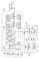
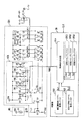
図1は、本発明に係る表示ドライバを含む表示装置100の構成を示すブロック図である。図1に示すように、表示装置100は、駆動制御部11、走査ドライバ12、データドライバ13、及び表示デバイス20を有する。
FIG. 1 is a block diagram showing a configuration of a
表示デバイス20は、例えば有機ELパネル又は液晶表示パネル等からなる。表示デバイス20には、2次元画面の水平方向に伸張する水平走査ラインS1〜Sm(mは2以上の整数)と、2次元画面の垂直方向に伸張するデータラインD1〜Dn(nは2以上の整数)と、が形成されている。水平走査ラインとデータラインとの各交叉部の領域(破線にて囲まれた領域)には表示セルが形成されている。
The
尚、水平走査ラインS1〜Smは走査ドライバ12に接続されており、データラインD1〜Dnはデータドライバ13に接続されている。
The horizontal scan lines S1 to Sm are connected to the
駆動制御部11は、映像信号VD中から水平同期信号を検出して走査ドライバ12に供給する。また、駆動制御部11は、映像信号VDに基づき画素の輝度レベルを例えば8ビットの輝度階調で表す画素データ片の列を含む画像データ信号PDを生成し、これをデータドライバ13に供給する。
The
走査ドライバ12は、駆動制御部11から供給された水平同期信号に同期したタイミングで、水平走査パルスを表示デバイス20の水平走査ラインS1〜Smの各々に順次印加する。
The
データドライバ13は、半導体IC(integrated circuit)チップに形成されており、データ取込部131、階調電圧生成部132及び出力アンプ部133を含む。
The
データ取込部131は、画像データ信号PDに含まれる画素データ片を1水平走査ライン分ずつ、つまりn個毎に取り込む。データ取込部131は、取り込んだn個の画素データ片を画素データP1〜Pnとし、これら画素データP1〜Pnを、クロック信号CLKの例えば立ち上がりエッジのタイミングで階調電圧生成部132に供給する。
The data taking-in
階調電圧生成部132は、データ取込部131から供給された画素データP1〜Pnを、夫々の輝度レベルに対応した電圧値を有する階調電圧V1〜Vnに変換して出力アンプ部133に供給する。
The gradation
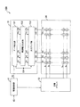
図2は、出力アンプ部133の内部構成の一例を示すブロック図である。図2に示すように、出力アンプ部133は、メインバイアス回路MB、サブバイアス回路SB1〜SB3、及び制御部CNを含むバイアス電圧生成部1330と、アンプAP1〜APnと、を有する。
FIG. 2 is a block diagram showing an example of the internal configuration of the
アンプAP1〜APnは、階調電圧V1〜Vnを増幅して得たn個の電圧を駆動電圧G1〜Gnとし、夫々を半導体ICチップの出力端子T1〜Tnを介して出力する。出力端子T1〜Tnは、表示デバイス20のデータラインD1〜Dnに夫々接続されている。
The amplifiers AP1 to APn use n voltages obtained by amplifying the gradation voltages V1 to Vn as drive voltages G1 to Gn, and output the respective voltages via the output terminals T1 to Tn of the semiconductor IC chip. The output terminals T1 to Tn are connected to data lines D1 to Dn of the
尚、アンプAP1〜APnの各々は、例えばオペアンプを含み、サブバイアス回路SB1〜SB3から供給されたバイアス電圧VBH1〜VBH3及びVBL1〜VBL3に応じて、当該オペアンプの差動段、並びにカレントミラー段に流す動作電流が設定される。これにより、アンプAP1〜APnの各々は、バイアス電圧VBH1〜VBH3及びVBL1〜VBL3に応じて自身の出力スルーレートが調整される。 Each of the amplifiers AP1 to APn includes, for example, an operational amplifier, and according to the bias voltages VBH1 to VBH3 and VBL1 to VBL3 supplied from the sub bias circuits SB1 to SB3, the differential stage of the operational amplifier and the current mirror stage The operating current to flow is set. Thus, each of the amplifiers AP1 to APn adjusts its output slew rate according to the bias voltages VBH1 to VBH3 and VBL1 to VBL3.
メインバイアス回路MBは、所定の一定電流を有する基準電流IBを生成し、これをサブバイアス回路SB1〜SB3に夫々供給する。 The main bias circuit MB generates a reference current IB having a predetermined constant current and supplies it to the sub bias circuits SB1 to SB3.
サブバイアス回路SB1〜SB3の各々は、基準電流IBに基づき、バイアス電圧制御信号PWRCに応じた電圧値を有するバイアス電圧VBH1〜VBH3及びVBL1〜VBL3を生成する。 Each of sub bias circuits SB1 to SB3 generates bias voltages VBH1 to VBH3 and VBL1 to VBL3 having voltage values corresponding to bias voltage control signal PWRC based on reference current IB.
サブバイアス回路SB1は、生成したバイアス電圧VBH1〜VBH3及びVBL1〜VBL3を、アンプAP1〜APnを3つのグループに区分けした際の第1のグループに属するAP1〜APr(rはn未満の整数)に供給する。サブバイアス回路SB2は、当該バイアス電圧VBH1〜VBH3及びVBL1〜VBL3を、アンプAP1〜APnのうちの第2のグループに属するAP(r+1)〜APg(gは、rより大であり且つn未満の整数)に供給する。サブバイアス回路SB3は、上記した電圧値の調整が施されたバイアス電圧VBH1〜VBH3及びVBL1〜VBL3を、アンプAP1〜APnのうちの第3のグループに属するAP(g+1)〜APnに供給する。 Sub bias circuit SB1 sets generated bias voltages VBH1 to VBH3 and VBL1 to VBL3 to AP1 to APr (r is an integer smaller than n) belonging to the first group when amplifiers AP1 to APn are divided into three groups. Supply. The sub bias circuit SB2 applies the bias voltages VBH1 to VBH3 and VBL1 to VBL3 to AP (r + 1) to APg (g is greater than r and less than n) belonging to the second group of the amplifiers AP1 to APn. Supply). The sub bias circuit SB3 supplies the bias voltages VBH1 to VBH3 and VBL1 to VBL3 subjected to the adjustment of the voltage values described above to AP (g + 1) to APn belonging to the third group among the amplifiers AP1 to APn.
制御部CNは、バイアス電圧VBH1〜VBH3及びVBL1〜VBL3の電圧値を設定するバイアス電圧制御信号PWRCを生成し、これをサブバイアス回路SB1〜SB3に供給する。 The control unit CN generates a bias voltage control signal PWRC for setting the voltage values of the bias voltages VBH1 to VBH3 and VBL1 to VBL3, and supplies this to the sub bias circuits SB1 to SB3.
以下に、制御部CN、メインバイアス回路MB、サブバイアス回路SB1〜SB3の内部構成について詳細に説明する。尚、サブバイアス回路SB1〜SB3各々の内部構成は同一であるので、当該サブバイアス回路SB1のみを抜粋して説明する。 The internal configuration of control unit CN, main bias circuit MB, and sub bias circuits SB1 to SB3 will be described in detail below. Since the internal configuration of each of the sub bias circuits SB1 to SB3 is the same, only the sub bias circuit SB1 will be extracted and described.
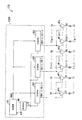
図3は、制御部CN、メインバイアス回路MB、及びサブバイアス回路SB1の内部構成の一例を表す図である。 FIG. 3 is a diagram showing an example of the internal configuration of control unit CN, main bias circuit MB, and sub bias circuit SB1.
制御部CNは、電圧遷移時バイアス設定レジスタRG1、出力一定時バイアス設定レジスタRG2、切換タイミングレジスタCRG及び制御信号生成部SGを含む。 The control unit CN includes a bias setting register RG1 at the time of voltage transition, a bias setting register RG2 at the time of constant output, a switching timing register CRG, and a control signal generation unit SG.
電圧遷移時バイアス設定レジスタRG1には、駆動電圧Gの立ち上がり又は立ち下がり期間中においてアンプAP1〜APrを高スルーレート化する為のバイアス電圧VBH1〜3、VBL1〜3の電圧値を示すバイアス電圧情報Bs1が記憶されている。電圧遷移時バイアス設定レジスタRG1は、バイアス電圧情報Bs1を制御信号生成部SGに供給する。 Bias voltage information indicating voltage values of bias voltages VBH1 to 3 and VBL1 to 3 for increasing the slew rate of the amplifiers AP1 to APr during the rising or falling period of the drive voltage G in the bias setting register RG1 at the time of voltage transition Bs1 is stored. At the time of voltage transition, the bias setting register RG1 supplies bias voltage information Bs1 to the control signal generation unit SG.
出力一定時バイアス設定レジスタRG2には、駆動電圧Gの電圧値の遷移量が所定値未満となる出力一定期間中においてアンプAP1〜APrを低消費電力化する為のバイアス電圧VBH1〜3、VBL1〜3の電圧値を示すバイアス電圧情報Bs2が記憶されている。出力一定時バイアス設定レジスタRG2は、バイアス電圧情報Bs2を制御信号生成部SGに供給する。 In the constant-output bias setting register RG2, bias voltages VBH1-3, VBL1-V for reducing the power consumption of the amplifiers AP1-APr during a constant output period in which the transition amount of the voltage value of the drive voltage G is less than a predetermined value. Bias voltage information Bs2 indicating a voltage value of 3 is stored. The constant output bias setting register RG2 supplies the bias voltage information Bs2 to the control signal generator SG.
切換タイミングレジスタCRGには、バイアス電圧VBH1〜3、VBL1〜3の電圧値を切り替えるタイミングを示す切換タイミング情報TGが記憶されている。切換タイミングレジスタCRGは、切換タイミング情報TGを制御信号生成部SGに供給する。 In the switching timing register CRG, switching timing information TG indicating the timing of switching the voltage values of the bias voltages VBH1 to 3 and VBL1 to 3 is stored. The switching timing register CRG supplies switching timing information TG to the control signal generator SG.
制御信号生成部SGは、クロック信号CLK、切換タイミング情報TG、バイアス電圧情報Bs1及びBs2に基づき、バイアス電圧制御信号PWRCを生成する。 The control signal generation unit SG generates a bias voltage control signal PWRC based on the clock signal CLK, the switching timing information TG, and the bias voltage information Bs1 and Bs2.
つまり、制御信号生成部SGは、クロック信号CLKの例えば立ち上がりエッジのタイミングで、先ず、バイアス電圧情報Bs1及びBs2のうちのBs1を取り込む。次に、制御信号生成部SGは、バイアス電圧情報Bs1にて示される電圧値を有するバイアス電圧(VBH1〜3、VBL1〜3)をサブバイアス回路SB1側で生成させる為のバイアス電圧制御信号PWRCを生成し、これを当該サブバイアス回路SB1に供給する。ここで、制御信号生成部SGは、切換タイミング情報TGにて示されるタイミングで、バイアス電圧情報Bs2を取り込む。そして、制御信号生成部SGは、バイアス電圧情報Bs2にて示される電圧値を有するバイアス電圧(VBH1〜3、VBL1〜3)をサブバイアス回路SB1側で生成させる為のバイアス電圧制御信号PWRCを生成し、これを当該サブバイアス回路SB1に供給する。 That is, the control signal generation unit SG first takes in Bs1 of the bias voltage information Bs1 and Bs2 at the timing of, for example, the rising edge of the clock signal CLK. Next, the control signal generation unit SG generates a bias voltage control signal PWRC for generating bias voltages (VBH1 to 3 and VBL1 to 3) having voltage values indicated by the bias voltage information Bs1 on the sub bias circuit SB1 side. It generates and supplies this to the sub-bias circuit SB1. Here, the control signal generation unit SG takes in the bias voltage information Bs2 at the timing indicated by the switching timing information TG. Then, control signal generation unit SG generates bias voltage control signal PWRC for generating bias voltages (VBH1 to 3 and VBL1 to 3) having voltage values indicated by bias voltage information Bs2 on the side of sub bias circuit SB1. And supplies this to the sub-bias circuit SB1.
尚、バイアス電圧制御信号PWRCは、例えば、図3に示すようにサブバイアス回路SB1に含まれるPチャネルMOS(Metal-Oxide-Semiconductor)型のトランジスタQ3〜Q5のうちで、オン状態に設定するトランジスタの数を指定する情報を含む。 The bias voltage control signal PWRC is, for example, a transistor set to an on state among the transistors Q3 to Q5 of P-channel MOS (Metal-Oxide-Semiconductor) type included in the sub-bias circuit SB1 as shown in FIG. Contains information that specifies the number of
メインバイアス回路MBは、電源電位VDDを受けて基準電流IBを生成し、これをノードL1を介してサブバイアス回路SB1に供給する電流源G1を有する。 Main bias circuit MB has a current source G1 receiving power supply potential VDD to generate reference current IB and supplying it to sub bias circuit SB1 via node L1.
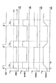
サブバイアス回路SB1は、PチャネルMOS型のトランジスタQ1〜Q5及びスイッチ回路SW1〜SW3を含む電圧調整部VCNと、PチャネルMOS型のトランジスタQ6〜Q12と、NチャネルMOS型のトランジスタR1〜R10と、を有する。 Sub bias circuit SB1 includes a voltage adjustment unit VCN including P channel MOS transistors Q1 to Q5 and switch circuits SW1 to SW3, P channel MOS transistors Q6 to Q12, and N channel MOS transistors R1 to R10. And.
トランジスタR1は、自身のドレイン端及びゲート端がノードL1とトランジスタR2のゲート端とに接続されている。トランジスタR1及びR2各々のソース端には接地電位VSSが印加されている。トランジスタR2のドレイン端は、ノードL2を介して電圧調整部VCNと接続されている。 The drain end and the gate end of the transistor R1 are connected to the node L1 and the gate end of the transistor R2. The ground potential VSS is applied to the source terminal of each of the transistors R1 and R2. The drain end of the transistor R2 is connected to the voltage adjustment unit VCN via the node L2.
かかる構成によりトランジスタR2は、基準電流IBに対応した電流I2をノードL2に流す。 With this configuration, the transistor R2 causes the current I2 corresponding to the reference current IB to flow to the node L2.
電圧調整部VCNのトランジスタQ1及びQ2各々のゲート端はノードL2に接続されている。トランジスタQ1及びQ各々のソース端には電源電位VDDが印加されている。トランジスタQ2のドレイン端は、ノードL3を介してトランジスタR3のドレイン端及びゲート端に接続されている。トランジスタR3のソース端には接地電位VSSが印加されている。 The gate terminal of each of the transistors Q1 and Q2 of the voltage adjustment unit VCN is connected to the node L2. The power supply potential VDD is applied to the source terminal of each of the transistors Q1 and Q. The drain end of the transistor Q2 is connected to the drain end and the gate end of the transistor R3 via the node L3. The ground potential VSS is applied to the source terminal of the transistor R3.
かかる構成により、トランジスタQ2は、上記した電流I2に対応した電流I3をノードL3に送出することにより、当該ノードL3に基準バイアス電圧VQを生成する。 With this configuration, the transistor Q2 generates the reference bias voltage VQ at the node L3 by transmitting the current I3 corresponding to the above-described current I2 to the node L3.
電圧調整部VCNのトランジスタQ3〜Q5各々のソース端には電源電位VDDが印加されており、夫々のドレイン端はノードL3に接続されている。 The power supply potential VDD is applied to the source terminal of each of the transistors Q3 to Q5 of the voltage adjustment unit VCN, and the drain terminal of each is connected to the node L3.
スイッチ回路SW1は、バイアス電圧制御信号PWRCに応じて、電源電位VDDをトランジスタQ3のゲート端に供給する状態(オフ状態と称する)、又はノードL2をトランジスタQ3のゲート端に接続する状態(オン状態と称する)に設定される。スイッチ回路SW2は、バイアス電圧制御信号PWRCに応じて、電源電位VDDをトランジスタQ4のゲート端に供給する状態(オフ状態と称する)、又はノードL2をトランジスタQ3のゲート端に接続する状態(オン状態と称する)に設定される。スイッチ回路SW3は、バイアス電圧制御信号PWRCに応じて、電源電位VDDをトランジスタQ5のゲート端に供給する状態(オフ状態と称する)、又はノードL2をトランジスタQ5のゲート端に接続する状態(オン状態と称する)に設定される。 Switch circuit SW1 supplies power supply potential VDD to the gate end of transistor Q3 (referred to as an off state) or connects node L2 to the gate end of transistor Q3 (on state) in response to bias voltage control signal PWRC. Is called). Switch circuit SW2 supplies power supply potential VDD to the gate terminal of transistor Q4 in response to bias voltage control signal PWRC (referred to as an off state), or connects node L2 to the gate terminal of transistor Q3 (on state Is called). Switch circuit SW3 supplies power supply potential VDD to the gate end of transistor Q5 (referred to as an off state) or connects node L2 to the gate end of transistor Q5 (on state) in response to bias voltage control signal PWRC. Is called).
トランジスタQ3は、スイッチ回路SW1がオン状態になる場合にだけオン状態となり、上記した電流I2に対応した電流IcをノードL3に送出する。トランジスタQ4は、スイッチ回路SW2がオン状態になる場合にだけオン状態となり、上記した電流I2に対応した電流IcをノードL3に送出する。トランジスタQ5は、スイッチ回路SW3がオン状態になる場合にだけオン状態となり、上記した電流I2に対応した電流IcをノードL3に送出する。 The transistor Q3 is turned on only when the switch circuit SW1 is turned on, and delivers the current Ic corresponding to the current I2 to the node L3. The transistor Q4 is turned on only when the switch circuit SW2 is turned on, and delivers the current Ic corresponding to the current I2 to the node L3. The transistor Q5 is turned on only when the switch circuit SW3 is turned on, and delivers the current Ic corresponding to the current I2 to the node L3.
上記した構成により、電圧調整部VCNは、基準電流IBに対応した電流I3と、バイアス電圧制御信号PWRCに応じてオン状態に設定されたトランジスタQ3〜Q5から送出された電流Icを合成した合成電流ItをノードL3に送出する。合成電流ItがノードL3に送出されることで生成された基準バイアス電圧VQの電圧値が調整される。 With the above-described configuration, voltage adjustment unit VCN is a combined current combining current I3 corresponding to reference current IB and current Ic sent from transistors Q3 to Q5 set to the on state according to bias voltage control signal PWRC. Send It to the node L3. The voltage value of the reference bias voltage VQ generated by transmitting the combined current It to the node L3 is adjusted.
例えば、電圧調整部VCNが、トランジスタQ3〜Q5のうちでオン状態に設定するトランジスタの数としてゼロを表すバイアス電圧制御信号PWRCを受けた場合には、ノードL3に流れる合成電流Itは電流I3となる。 For example, when voltage adjustment unit VCN receives bias voltage control signal PWRC representing zero as the number of transistors Q3 to Q5 to be turned on, combined current It flowing to node L3 is current I3 and Become.
また、電圧調整部VCNが、トランジスタQ3〜Q5のうちでオン状態に設定するトランジスタの数として「2」を表すバイアス電圧制御信号PWRCを受けた場合には、例えばトランジスタQ3〜Q5のうちのQ3及びQ4のみがオン状態に設定される。これにより合成電流Itは、電流I3にトランジスタQ3及びQ4の各々から送出された電流Icを加えた電流(I3+2・Ic)となる。 When voltage adjustment unit VCN receives bias voltage control signal PWRC representing "2" as the number of transistors to be turned on among transistors Q3 to Q5, for example, Q3 of transistors Q3 to Q5. And Q4 are set to the on state. As a result, the combined current It becomes a current (I3 + 2 · Ic) obtained by adding the current Ic sent from each of the transistors Q3 and Q4 to the current I3.
すなわち、図3に示す電圧調整部VCNは、バイアス電圧制御信号PWRCに応じて4段階で基準バイアス電圧VQの電圧値を調整することにより、バイアス電圧情報Bs1又はBs2にて示される電圧値を有する基準バイアス電圧VQを生成する。 That is, voltage adjustment unit VCN shown in FIG. 3 has a voltage value indicated by bias voltage information Bs1 or Bs2 by adjusting the voltage value of reference bias voltage VQ in four steps according to bias voltage control signal PWRC. A reference bias voltage VQ is generated.
図3において、トランジスタR4〜R7各々のゲート端は上記したトランジスタR3のゲート端及びノードL3に接続されており、トランジスタR4〜R7各々のソース端には接地電位VSSが印加されている。トランジスタR4のドレイン端は、ノードL4を介してトランジスタQ6のゲート端及びドレイン端に接続されている。トランジスタR5のドレイン端は、ノードL5を介してトランジスタQ7のゲート端及びドレイン端に接続されている。トランジスタR6のドレイン端は、ノードL6を介してトランジスタQ8のゲート端及びドレイン端に接続されている。トランジスタQ6〜Q8各々のソース端には電源電位VDDが印加されている。 In FIG. 3, the gate ends of the transistors R4 to R7 are connected to the gate end of the transistor R3 and the node L3, respectively, and the ground potential VSS is applied to the source ends of the transistors R4 to R7. The drain end of the transistor R4 is connected to the gate end and the drain end of the transistor Q6 via the node L4. The drain end of the transistor R5 is connected to the gate end and the drain end of the transistor Q7 via the node L5. The drain end of the transistor R6 is connected to the gate end and the drain end of the transistor Q8 via the node L6. The power supply potential VDD is applied to the source terminal of each of the transistors Q6 to Q8.
トランジスタR7のドレイン端は、トランジスタQ9のドレイン端、及びトランジスタQ9〜Q12各々のゲート端に接続されている。トランジスタQ9〜Q12各々のソース端には電源電位VDDが印加されている。トランジスタQ10のドレイン端はノードL7を介してトランジスタR8のゲート端及びドレイン端に接続されている。トランジスタQ11のドレイン端はノードL8を介してトランジスタR9のゲート端及びドレイン端に接続されている。トランジスタQ12のドレイン端はノードL9を介してトランジスタR9のゲート端及びドレイン端に接続されている。トランジスタR8〜R10各々のソース端には接地電位VSSが印加されている。 The drain end of the transistor R7 is connected to the drain end of the transistor Q9 and the gate end of each of the transistors Q9 to Q12. The power supply potential VDD is applied to the source terminal of each of the transistors Q9 to Q12. The drain end of the transistor Q10 is connected to the gate end and the drain end of the transistor R8 via the node L7. The drain end of the transistor Q11 is connected to the gate end and the drain end of the transistor R9 via the node L8. The drain end of the transistor Q12 is connected to the gate end and the drain end of the transistor R9 via the node L9. The ground potential VSS is applied to the source terminal of each of the transistors R8 to R10.
上記したトランジスタR4及びQ6からなる回路では、トランジスタR4が、自身のゲート端に供給された基準バイアス電圧VQに対応した電流をノードL4に流す。これによって当該ノードL4に生じた電圧が、バイアス電圧VBH1としてアンプAP1〜APrに供給される。 In the circuit composed of the transistors R4 and Q6 described above, the transistor R4 flows a current corresponding to the reference bias voltage VQ supplied to its gate terminal to the node L4. As a result, the voltage generated at the node L4 is supplied as the bias voltage VBH1 to the amplifiers AP1 to APr.
トランジスタR5及びQ7からなる回路では、トランジスタR5が、自身のゲート端に供給された基準バイアス電圧VQに対応した電流をノードL5に流す。これによって当該ノードL5に生じた電圧が、バイアス電圧VBH2としてアンプAP1〜APrに供給される。 In the circuit composed of the transistors R5 and Q7, the transistor R5 flows a current corresponding to the reference bias voltage VQ supplied to its gate terminal to the node L5. As a result, the voltage generated at the node L5 is supplied as the bias voltage VBH2 to the amplifiers AP1 to APr.
トランジスタR6及びQ8からなる回路では、トランジスタR6が、自身のゲート端に供給された基準バイアス電圧VQに対応した電流をノードL6に流す。これによって当該ノードL6に生じた電圧が、バイアス電圧VBH3としてアンプAP1〜APrに供給される。 In the circuit composed of the transistors R6 and Q8, the transistor R6 flows a current corresponding to the reference bias voltage VQ supplied to its gate terminal to the node L6. As a result, the voltage generated at the node L6 is supplied as the bias voltage VBH3 to the amplifiers AP1 to APr.
尚、トランジスタR7は、自身のゲート端に供給された基準バイアス電圧VQに対応した電流をトランジスタQ9を介して流す。これにより、当該基準バイアス電圧VQに対応した電流が、トランジスタQ10〜Q12の各々のドレイン端からノードL7〜L9に夫々送出される。 The transistor R7 causes a current corresponding to the reference bias voltage VQ supplied to its own gate terminal to flow through the transistor Q9. Thereby, currents corresponding to the reference bias voltage VQ are respectively sent from the drain end of each of the transistors Q10 to Q12 to the nodes L7 to L9.
この際、トランジスタQ10が基準バイアス電圧VQに対応した電流をノードL7に送出することによって当該ノードL7に生じた電圧が、バイアス電圧VBL1としてアンプAP1〜APrに供給される。また、トランジスタQ11が基準バイアス電圧VQに対応した電流をノードL8に送出することによって当該ノードL8に生じた電圧が、バイアス電圧VBL2としてアンプAP1〜APrに供給される。また、トランジスタQ12が基準バイアス電圧VQに対応した電流をノードL9に送出することによって当該ノードL9に生じた電圧が、バイアス電圧VBL3としてアンプAP1〜APrに供給される。 At this time, the transistor Q10 sends out a current corresponding to the reference bias voltage VQ to the node L7, and the voltage generated at the node L7 is supplied to the amplifiers AP1 to APr as the bias voltage VBL1. Further, the transistor Q11 sends out a current corresponding to the reference bias voltage VQ to the node L8, and a voltage generated at the node L8 is supplied to the amplifiers AP1 to APr as the bias voltage VBL2. Further, the transistor Q12 sends out a current corresponding to the reference bias voltage VQ to the node L9, and the voltage generated at the node L9 is supplied to the amplifiers AP1 to APr as the bias voltage VBL3.
アンプAP1〜APrの各々は同一の内部構成を有する。そこで、以下にアンプAP1〜APrのうちのAP1を抜粋して、その内部構成について詳細に説明する。 Each of the amplifiers AP1 to APr has the same internal configuration. Therefore, below, AP1 of the amplifiers AP1 to APr will be extracted and the internal configuration thereof will be described in detail.
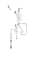
図4は、アンプAP1の内部構成を概略的に表すブロック図である。図4に示すように、アンプAP1は、オペアンプOPA及び出力スイッチOSWを含む。 FIG. 4 is a block diagram schematically showing an internal configuration of the amplifier AP1. As shown in FIG. 4, the amplifier AP1 includes an operational amplifier OPA and an output switch OSW.
オペアンプOPAは、出力端と反転入力端とが接続されている、いわゆるボルテージフォロワからなり、非反転入力端で受けた階調電圧V1を利得1で増幅して得られた出力電圧Y1を出力スイッチOSWに供給する。オペアンプOPAは、バイアス電圧VBH1〜VBH3及びVBL1〜VBL3に応じて自身の動作電流を調整することにより、出力スルーレートを変更する。出力スイッチOSWは、オン状態時にのみ、出力電圧Y1を駆動電圧G1として、半導体ICチップの出力端子T1から出力する。 The operational amplifier OPA comprises a so-called voltage follower in which an output end and an inverting input end are connected, and an output switch Y1 obtained by amplifying the gradation voltage V1 received at the non-inverting input end with a gain of 1 Supply to OSW. The operational amplifier OPA changes the output slew rate by adjusting its own operating current in accordance with the bias voltages VBH1 to VBH3 and VBL1 to VBL3. The output switch OSW outputs the output voltage Y1 as the drive voltage G1 from the output terminal T1 of the semiconductor IC chip only in the on state.
図5は、オペアンプOPAの内部構成を表す回路図である。オペアンプOPAは、差動段DFP、カレントミラー段CMR及び出力段OUPを含む。 FIG. 5 is a circuit diagram showing an internal configuration of the operational amplifier OPA. The operational amplifier OPA includes a differential stage DFP, a current mirror stage CMR and an output stage OUP.
差動段DFPは、PチャネルMOS型のトランジスタU1〜U4、及びNチャネルMOS型のトランジスタJ1〜J4を含む。 The differential stage DFP includes P channel MOS type transistors U1 to U4 and N channel MOS type transistors J1 to J4.
トランジスタU1のソース端には電源電位VDDが印加されており、ゲート端にはバイアス電圧VBH1が供給されている。トランジスタU1のドレイン端はトランジスタU2のソース端に接続されている。トランジスタU2のゲート端にはバイアス電圧VBH2が供給されており、ドレイン端はトランジスタU3及びU4各々のソース端に接続されている。 The power supply potential VDD is applied to the source terminal of the transistor U1, and the bias voltage VBH1 is supplied to the gate terminal. The drain end of the transistor U1 is connected to the source end of the transistor U2. The bias voltage VBH2 is supplied to the gate terminal of the transistor U2, and the drain terminal is connected to the source terminal of each of the transistors U3 and U4.
かかる構成により、トランジスタU1及びU2は、電源電位VDDに基づき、バイアス電圧VBH1及びVBH2に応じた電流値を有する動作電流Iu1を生成し、これをトランジスタU3及びU4に供給する。 With such a configuration, the transistors U1 and U2 generate the operating current Iu1 having a current value corresponding to the bias voltages VBH1 and VBH2 based on the power supply potential VDD, and supply this to the transistors U3 and U4.
トランジスタU3及びU4は、夫々のゲート端で受けた階調電圧V1とこのオペアンプOPAの出力である出力電圧Y1との電圧比で、トランジスタU2から供給された動作電流Iu1を2分割した電流を電流NCM1及びNCM2として生成する。トランジスタU3及びU4は、電流NCM1及びNCM2を夫々のドレイン端を介してカレントミラー段CMRのノードn3及びn4に供給する。 The transistors U3 and U4 are currents obtained by dividing the operating current Iu1 supplied from the transistor U2 into two at a voltage ratio between the gradation voltage V1 received at each gate terminal and the output voltage Y1 output from the operational amplifier OPA. Generate as NCM1 and NCM2. The transistors U3 and U4 supply the currents NCM1 and NCM2 to the nodes n3 and n4 of the current mirror stage CMR via their respective drain ends.
すなわち、トランジスタU3は、階調電圧V1の電圧値に対応した電流NCM2をカレントミラー段CMRのノードn4に供給する。トランジスタU4は、出力電圧Y1の電圧値に対応した電流NCM1をカレントミラー段CMRのノードn3に供給する。 That is, transistor U3 supplies current NCM2 corresponding to the voltage value of gradation voltage V1 to node n4 of current mirror stage CMR. The transistor U4 supplies a current NCM1 corresponding to the voltage value of the output voltage Y1 to the node n3 of the current mirror stage CMR.
トランジスタJ1のソース端には接地電位VSSが印加されており、ゲート端にはバイアス電圧VBL1が供給されている。トランジスタJ1のドレイン端はトランジスタJ2のソース端に接続されている。トランジスタJ2のゲート端にはバイアス電圧VBL2が供給されており、ドレイン端はトランジスタJ3及びJ4各々のソース端に接続されている。 The ground potential VSS is applied to the source terminal of the transistor J1, and the bias voltage VBL1 is supplied to the gate terminal. The drain end of the transistor J1 is connected to the source end of the transistor J2. The bias voltage VBL2 is supplied to the gate terminal of the transistor J2, and the drain terminal is connected to the source terminal of each of the transistors J3 and J4.
かかる構成により、トランジスタJ1及びJ2は、バイアス電圧VBL1及びVBL2に応じた電流値を有する動作電流Ij1を生成し、これをトランジスタJ3及びJ4のソース端から引き抜く。 With this configuration, the transistors J1 and J2 generate the operating current Ij1 having a current value corresponding to the bias voltages VBL1 and VBL2, and this is extracted from the source end of the transistors J3 and J4.
トランジスタJ3及びJ4は、夫々のゲート端で受けた階調電圧V1と出力電圧Y1との電圧比で動作電流Ij1を2分割した電流を電流PCM1及びPCM2として生成する。トランジスタJ3及びJ4は、電流PCM1及びPCM2を夫々のドレイン端を介してカレントミラー段CMRのノードn1及びn2から引き抜く。 The transistors J3 and J4 generate currents as PCM1 and PCM2 by dividing the operating current Ij1 into two by the voltage ratio of the gradation voltage V1 received at each gate terminal and the output voltage Y1. The transistors J3 and J4 draw the currents PCM1 and PCM2 from the nodes n1 and n2 of the current mirror stage CMR via their respective drain ends.
すなわち、トランジスタJ3は、階調電圧V1に対応した電流PCM2をカレントミラー段CMRのノードn2から引き抜き、これをトランジスタJ2のドレイン端に供給する。トランジスタJ4は、出力電圧Y1に対応した電流PCM1をカレントミラー段CMRのノードn1から引き抜き、これをトランジスタJ2のドレイン端に供給する。 That is, the transistor J3 extracts the current PCM2 corresponding to the gradation voltage V1 from the node n2 of the current mirror stage CMR, and supplies it to the drain end of the transistor J2. The transistor J4 draws the current PCM1 corresponding to the output voltage Y1 from the node n1 of the current mirror stage CMR, and supplies it to the drain end of the transistor J2.
尚、差動段DFPでは、バイアス電圧VBH1及びVBH2に応じて上記した動作電流Iu1の電流値が調整され、更に、バイアス電圧VBL1及びVBL2に応じて上記した動作電流Ij1の電流値が調整される。これにより、例えばバイアス電圧VBH1及びVBH2の電圧値が低いほど大きな電流がカレントミラー段CMRのノードn3及びn4に供給される。また、例えばバイアス電圧VBL1及びVBL2の電圧値が高いほど大きな電流がカレントミラー段CMRのノードn1及びn2から引き抜かれる。 In differential stage DFP, the current value of operating current Iu1 described above is adjusted according to bias voltages VBH1 and VBH2, and the current value of operating current Ij1 described above is further adjusted according to bias voltages VBL1 and VBL2. . As a result, for example, as the voltage values of the bias voltages VBH1 and VBH2 decrease, a larger current is supplied to the nodes n3 and n4 of the current mirror stage CMR. Also, for example, as the voltage values of the bias voltages VBL1 and VBL2 increase, larger currents are extracted from the nodes n1 and n2 of the current mirror stage CMR.
カレントミラー段CMRは、PチャネルMOS型のトランジスタU5〜U10、及びNチャネルMOS型のトランジスタJ5〜J10を含む。 The current mirror stage CMR includes P channel MOS type transistors U5 to U10 and N channel MOS type transistors J5 to J10.
トランジスタU5及びU6各々のソース端には電源電位VDDが印加されており、夫々のゲート端は互いに接続されている。トランジスタU5のドレイン端はノードn1を介してトランジスタU7のソース端に接続されている。トランジスタU6のドレイン端はノードn2を介してトランジスタU8のソース端に接続されている。 The power supply potential VDD is applied to the source terminal of each of the transistors U5 and U6, and their gate terminals are connected to each other. The drain end of the transistor U5 is connected to the source end of the transistor U7 via the node n1. The drain end of the transistor U6 is connected to the source end of the transistor U8 via the node n2.
トランジスタU7及びU8のゲート端には共にバイアス電圧VBH3が印加されている。トランジスタU7のドレイン端は、ノードn5を介して上記したトランジスタU5及びU6各々のゲート端と、トランジスタU9のソース端と、トランジスタJ5のドレイン端とに接続されている。 A bias voltage VBH3 is applied to the gate terminals of the transistors U7 and U8. The drain end of the transistor U7 is connected to the gate end of each of the transistors U5 and U6, the source end of the transistor U9, and the drain end of the transistor J5 via the node n5.
トランジスタU8のドレイン端は、高電位側の駆動ノードとしてのノードn6を介してトランジスタU10のソース端及びトランジスタJ6のドレイン端に接続されている。 The drain end of the transistor U8 is connected to the source end of the transistor U10 and the drain end of the transistor J6 via a node n6 as a high potential side drive node.
トランジスタU9及びU10各々のゲート端にはバイアス電圧VBH3が印加されている。トランジスタU9のドレイン端及びトランジスタJ5のソース端は、ノードn7を介してトランジスタJ7のドレイン端に接続されている。 A bias voltage VBH3 is applied to the gate terminal of each of the transistors U9 and U10. The drain end of the transistor U9 and the source end of the transistor J5 are connected to the drain end of the transistor J7 via the node n7.
トランジスタU10のドレイン端及びトランジスタJ6のソース端は、低電位側の駆動ノードとしてのノードn8を介してトランジスタJ8のドレイン端に接続されている。トランジスタJ5及びJ6各々のゲート端にはバイアス電圧VBL3が印加されている。 The drain end of the transistor U10 and the source end of the transistor J6 are connected to the drain end of the transistor J8 via a node n8 as a drive node on the low potential side. A bias voltage VBL3 is applied to the gate terminal of each of the transistors J5 and J6.
トランジスタJ7及びJ8各々のゲート端にはバイアス電圧VBL3が印加されている。トランジスタJ7のソース端はノードn3を介してトランジスタJ9のドレイン端に接続されている。トランジスタJ8のソース端は、ノードn4を介してトランジスタJ10のドレイン端に接続されている。 A bias voltage VBL3 is applied to the gate terminal of each of the transistors J7 and J8. The source end of the transistor J7 is connected to the drain end of the transistor J9 via the node n3. The source end of the transistor J8 is connected to the drain end of the transistor J10 via the node n4.
トランジスタJ9及びJ10各々のソース端には接地電位VSSが印加されており、これらトランジスタJ9及びJ10各々のゲート端はトランジスタJ7のドレイン端に接続されている。 The ground potential VSS is applied to the source terminal of each of the transistors J9 and J10, and the gate terminal of each of the transistors J9 and J10 is connected to the drain terminal of the transistor J7.
上記した構成により、カレントミラー段CMRでは、差動段DFPから供給された電流PCM1と電流PCM2との差に対応した電流値を有する動作電流Iu2がノードn6に流れる。更に、カレントミラー段CMRでは、差動段DFPから供給された電流NCM1と電流NCM2との差に対応した電流値を有する動作電流Ij2がノードn8に流れる。 With the above configuration, in current mirror stage CMR, operating current Iu2 having a current value corresponding to the difference between current PCM1 and current PCM2 supplied from differential stage DFP flows to node n6. Further, in current mirror stage CMR, operating current Ij2 having a current value corresponding to the difference between current NCM1 and current NCM2 supplied from differential stage DFP flows to node n8.
これにより、カレントミラー段CMRでは、電流PCM1と電流PCM2との差に対応した動作電流Iu2を、駆動ノードとしてのノードn6に供給する又はノードn6から引き抜くことにより、ノードn6に高電位側の出力駆動電圧PGを生成する。カレントミラー段CMRは、当該出力駆動電圧PGを出力段OUPのPチャネルMOS型のトランジスタU11のゲート端に供給する。 Thereby, in the current mirror stage CMR, the operation current Iu2 corresponding to the difference between the current PCM1 and the current PCM2 is supplied to the node n6 as a drive node or pulled out from the node n6 to output the high potential side to the node n6. The drive voltage PG is generated. The current mirror stage CMR supplies the output drive voltage PG to the gate terminal of the P-channel MOS transistor U11 of the output stage OUP.
また、カレントミラー段CMRでは、電流NCM1と電流NCM2との差に対応した動作電流Ij2を、駆動ノードとしてのノードn8に供給する又はノードn8から引き抜くことにより、ノードn8に低電位側の出力駆動電圧NGを生成する。カレントミラー段CMRは、当該出力駆動電圧NGを出力段OUPのNチャネルMOS型のトランジスタJ11のゲート端に供給する。 Further, in current mirror stage CMR, output current driving on the low potential side of node n8 is performed by supplying operating current Ij2 corresponding to the difference between current NCM1 and current NCM2 to node n8 as a driving node or extracting it from node n8. Generate voltage NG. The current mirror stage CMR supplies the output drive voltage NG to the gate terminal of the N-channel MOS transistor J11 of the output stage OUP.
出力段OUPは、上記したトランジスタU11及びJ11の他に、位相補償用のキャパシタC1及びC2を含む。 Output stage OUP includes, in addition to transistors U11 and J11 described above, capacitors C1 and C2 for phase compensation.
キャパシタC1の一端は、カレントミラー段CMRのノードn2に接続されており、その他端は出力ノードnZに接続されている。キャパシタC2の一端は、カレントミラー段CMRのノードn4に接続されており、その他端は出力ノードnZに接続されている。 One end of the capacitor C1 is connected to the node n2 of the current mirror stage CMR, and the other end is connected to the output node nZ. One end of the capacitor C2 is connected to the node n4 of the current mirror stage CMR, and the other end is connected to the output node nZ.
トランジスタU11のソース端には電源電位VDDが印加されており、そのゲート端には上記した出力駆動電圧PGが供給されている。トランジスタU11は、電源電位に基づき、出力駆動電圧PGに対応した電流を生成し、これを出力ノードnZに供給することにより、出力ノードnZの電位を増加させる。 The power supply potential VDD is applied to the source terminal of the transistor U11, and the output drive voltage PG described above is supplied to the gate terminal thereof. The transistor U11 generates a current corresponding to the output drive voltage PG based on the power supply potential, and supplies the current to the output node nZ to increase the potential of the output node nZ.
トランジスタJ11のソース端には接地電位VSSが印加されており、そのゲート端には上記した出力駆動電圧NGが供給されている。トランジスタJ11は、出力駆動電圧NGに対応した電流を出力ノードnZから引き抜くことにより、出力ノードnZの電位を低下させる。 The ground potential VSS is applied to the source end of the transistor J11, and the output drive voltage NG described above is supplied to the gate end thereof. The transistor J11 lowers the potential of the output node nZ by extracting a current corresponding to the output drive voltage NG from the output node nZ.
上記したトランジスタU11及びJ11の動作により、出力ノードnZに出力電圧Y1が生成され、これが出力端子を介して出力される。この際、出力された出力電圧Y1が差動段DFPの高電位側のトランジスタU4のゲート端、及び低電位側のトランジスタJ4のゲート端の各々に帰還して供給される。 By the operation of the transistors U11 and J11 described above, an output voltage Y1 is generated at the output node nZ, and this is output via the output terminal. At this time, the output voltage Y1 output is fed back to the gate terminal of the transistor U4 on the high potential side of the differential stage DFP and the gate terminal of the transistor J4 on the low potential side.
ところで、カレントミラー段CMRでは、バイアス電圧VBH3及びVBL3に応じて、上記した駆動ノードとしてのノードn6及びn8に流れる動作電流Iu2及びIj2の電流値が調整される。 By the way, in the current mirror stage CMR, the current values of the operating currents Iu2 and Ij2 flowing to the nodes n6 and n8 as drive nodes are adjusted according to the bias voltages VBH3 and VBL3.
例えばバイアス電圧VBH3の電圧値が低いほど、駆動ノードとしてのノードn6に流れる動作電流Iu2が大きくなり、バイアス電圧VBL3の電圧値が高いほど、駆動ノードとしてのノードn8に流れる動作電流Ij2が大きくなる。これにより、出力駆動電圧PG及びNGの立ち上がり時間及び立ち下がり時間が速くなるので、オペアンプOPAのスルーレートが高くなる。 For example, the lower the voltage value of bias voltage VBH3, the larger the operating current Iu2 flowing to node n6 as a driving node, and the higher the voltage value of bias voltage VBL3, the larger the operating current Ij2 flowing to node n8 as a driving node . As a result, since the rise time and fall time of the output drive voltages PG and NG become faster, the slew rate of the operational amplifier OPA becomes higher.
一方、バイアス電圧VBH3の電圧値が高いほど、駆動ノードとしてのノードn6に流れる動作電流Iu2が小さくなり、バイアス電圧VBL3の電圧値が低いほど、駆動ノードとしてのノードn8に流れる動作電流Ij2が小さくなる。これにより、オペアンプOPAの電力消費量が低下する。 On the other hand, the higher the voltage value of bias voltage VBH3, the smaller operating current Iu2 flowing to node n6 as the driving node, and the lower the voltage value of bias voltage VBL3, the smaller the operating current Ij2 flowing to node n8 as the driving node Become. This reduces the power consumption of the operational amplifier OPA.
要するに、オペアンプOPAは、以下の動作を行う差動段、カレントミラー段、出力段及びバイアス調整部を含んでいる。すなわち、差動段(DFP)は、入力される階調電圧(V)と出力される出力電圧(Y)との電圧比で第1の動作電流(Iu1、Ij1)を2分割した第1の電流(PCM1、NCM1)及び第2の電流(PCM2、NCM2)を生成する。カレントミラー段(CMR)は、第1の電流と第2の電流との差に対応した第2の動作電流(Iu2、Ij2)を、駆動ノード(n6、n8)に供給する又は当該駆動ノードから引き抜くことにより、駆動ノードに出力駆動電圧(PG、NG)を生成する。出力段(OUP)は、当該出力駆動電圧に対応した出力電流を、出力ノード(nZ)に供給又は出力ノードから引き抜くことにより、出力ノードに出力電圧(Y)を生成する。バイアス調整部(U1、U2、J1、J2、U8、U10、J6、J8)は、バイアス電圧(VBH1〜3、VBL1〜3)に応じて、第1の動作電流(Iu1、Ij1)及び第2の動作電流(Iu2、Ij2)の電流値を調整する。 In short, the operational amplifier OPA includes a differential stage performing the following operations, a current mirror stage, an output stage, and a bias adjustment unit. That is, in the differential stage (DFP), the first operating current (Iu1, Ij1) is divided into two by a voltage ratio between the input gradation voltage (V) and the output voltage (Y) to be output. A current (PCM1, NCM1) and a second current (PCM2, NCM2) are generated. The current mirror stage (CMR) supplies a second operating current (Iu2, Ij2) corresponding to the difference between the first current and the second current to the drive nodes (n6, n8) or from the drive node By pulling out, an output drive voltage (PG, NG) is generated at the drive node. The output stage (OUP) generates an output voltage (Y) at the output node by supplying an output current corresponding to the output drive voltage to the output node (nZ) or extracting the output current from the output node. The bias adjusting units (U1, U2, J1, J2, U8, U10, J6, and J8) receive the first operating current (Iu1, Ij1) and the second operating current according to the bias voltages (VBH1 to 3 and VBL1 to 3). Adjust the current value of the operating current (Iu2, Ij2) of
次に、図3に示す構成の動作について説明する。 Next, the operation of the configuration shown in FIG. 3 will be described.
図6は、図3に示す制御信号生成部SGが生成するバイアス電圧制御信号PWRCの一例と、アンプAP1〜APrのうちのAP1の内部に流れる動作電流の推移と、を表すタイムチャートである。 FIG. 6 is a time chart showing an example of the bias voltage control signal PWRC generated by the control signal generation unit SG shown in FIG. 3 and transition of the operating current flowing in AP1 of the amplifiers AP1 to APr.
ここで、切換タイミングレジスタCRGには、図6に示すようにクロック信号CLKの立ち上がりエッジの時点から、高スルーレート期間Tst(以下、高SR期間Tstとも称する)経過した時点を切換タイミングとして表す切換タイミング情報TGが記憶されているものとする。尚、高SR期間Tstは、例えばアンプAPに入力された階調電圧が最低輝度を表す状態から最高輝度を表す状態に遷移した際に、駆動電圧Gが最低輝度を表す電圧値から、最高輝度を表す電圧値に遷移するまでに掛かる時間に、所定のマージン期間を加えた期間である。 Here, in the switching timing register CRG, as shown in FIG. 6, switching timing is represented as switching timing when a high slew rate period Tst (hereinafter also referred to as high SR period Tst) elapses from the timing of the rising edge of the clock signal CLK. It is assumed that timing information TG is stored. In the high SR period Tst, for example, when the gray scale voltage input to the amplifier AP transitions from the state representing the lowest luminance to the state representing the highest luminance, the driving voltage G has the highest luminance from the voltage value representing the lowest luminance. Is a period obtained by adding a predetermined margin period to the time taken to transit to the voltage value representing.
図6において、制御信号生成部SGは、先ず、クロック信号CLKの立ち上がりエッジの時点Tuから、切換タイミング情報TGにて示される高SR期間Tstに亘り、以下のバイアス電圧制御信号PWRCを生成し、これをサブバイアス回路SB1に供給する。すなわち、制御信号生成部SGは、バイアス電圧情報Bs1にて示される電圧値、つまり各アンプを高スルーレート化する電圧値を有するバイアス電圧をサブバイアス回路SB1側で生成させる為のバイアス電圧制御信号PWRCを生成する。例えば、制御信号生成部SGは、3つのトランジスタQ3〜Q5を全てオン状態に設定することを表す、信号レベルLVaを有するバイアス電圧制御信号PWRCを生成し、これをサブバイアス回路SB1に供給する。 In FIG. 6, the control signal generation unit SG first generates the following bias voltage control signal PWRC from the time point Tu of the rising edge of the clock signal CLK to the high SR period Tst indicated by the switch timing information TG, This is supplied to the sub bias circuit SB1. That is, control signal generation unit SG generates a bias voltage having a voltage value indicated by bias voltage information Bs1, that is, a bias voltage having a voltage value for increasing the slew rate of each amplifier on the side of sub bias circuit SB1. Generate a PWRC. For example, the control signal generation unit SG generates a bias voltage control signal PWRC having a signal level LVa indicating that all three transistors Q3 to Q5 are set to the on state, and supplies this to the sub bias circuit SB1.
かかるバイアス電圧制御信号PWRCに応じて、サブバイアス回路SB1の電圧調整部VCNは、合成電流It(I3+3・Ic)をノードL3に送出することにより、基準バイアス電圧VQの電圧値を調整する。サブバイアス回路SB1は、電圧値の調整が施された基準バイアス電圧VQに基づき、バイアス電圧情報Bs1にて示されている電圧値に対応した電圧値を有するバイアス電圧VBH1〜3、VBL1〜3を生成し、アンプAP1〜APrに供給する。 In response to the bias voltage control signal PWRC, the voltage adjustment unit VCN of the sub bias circuit SB1 adjusts the voltage value of the reference bias voltage VQ by transmitting the combined current It (I3 + 3 · Ic) to the node L3. Sub bias circuit SB1 sets bias voltages VBH1 to 3 and VBL1 to 3 having voltage values corresponding to the voltage value indicated by bias voltage information Bs1 based on reference bias voltage VQ subjected to voltage value adjustment. It generates and supplies to amplifiers AP1 to APr.
そして、当該高SR期間Tstが経過した時点Td以降、次のクロック信号CLKの立ち上がりエッジの時点までの間に亘り、制御信号生成部SGは、以下のバイアス電圧制御信号PWRCを生成する。すなわち、制御信号生成部SGは、バイアス電圧情報Bs2にて示されている電圧値、つまり各アンプを低消費電力化させる電圧値を有するバイアス電圧をサブバイアス回路SB1側で生成させる為のバイアス電圧制御信号PWRCを生成する。 The control signal generation unit SG generates the following bias voltage control signal PWRC from the time Td when the high SR period Tst has elapsed to the time of the rising edge of the next clock signal CLK. In other words, the control signal generation unit SG generates a bias voltage having a voltage value indicated by the bias voltage information Bs2, that is, a voltage value for reducing the power consumption of each amplifier on the sub bias circuit SB1 side. Generate control signal PWRC.
例えば、制御信号生成部SGは、3つのトランジスタQ3〜Q5を全てオフ状態に設定することを表す、信号レベルLVbを有するバイアス電圧制御信号PWRCを生成し、これをサブバイアス回路SB1に供給する。 For example, the control signal generation unit SG generates a bias voltage control signal PWRC having a signal level LVb indicating that all three transistors Q3 to Q5 are set to the off state, and supplies this to the sub bias circuit SB1.
かかるバイアス電圧制御信号PWRCによると、サブバイアス回路SB1の電圧調整部VCNは、電流I3によって生成された基準バイアス電圧VQに対して電圧値を変更する調整は行わない。よって、この際、サブバイアス回路SB1は、電流I3のみによって生成された基準バイアス電圧VQに基づき、バイアス電圧情報Bs2にて示されている電圧値に対応した電圧値を有するバイアス電圧VBH1〜3、VBL1〜3を生成し、アンプAP1〜APrに供給する。 According to the bias voltage control signal PWRC, the voltage adjustment unit VCN of the sub bias circuit SB1 does not adjust the reference bias voltage VQ generated by the current I3 to change the voltage value. Therefore, at this time, sub bias circuit SB1 has bias voltages VBH1 to VBH3 having voltage values corresponding to the voltage value indicated by bias voltage information Bs2 based on reference bias voltage VQ generated by current I3 alone. VBL1 to 3 are generated and supplied to the amplifiers AP1 to APr.
上記動作によれば、図6に示すように、クロック信号CLKの立ち上がり時点Tuから高SR期間Tstの間に、各アンプAPの差動段DFP、及びカレントミラー段CMRに流れる動作電流は、高SR期間Tstの経過時点以降に流れる動作電流に比べて大きい。 According to the above operation, as shown in FIG. 6, the operating current flowing through the differential stage DFP of each amplifier AP and the current mirror stage CMR is high during the high SR period Tst from the rise time Tu of the clock signal CLK. It is larger than the operating current flowing after the point in time when the SR period Tst has elapsed.
これにより、高速応答が要求される駆動電圧の立ち上がり又は立ち下がり区間中は、アンプAPのスルーレートが高くなるので、アンプAPから出力される駆動電圧の立ち上がり又は立ち下がり時間も短くなる。 As a result, since the slew rate of the amplifier AP is high during the rising or falling period of the driving voltage for which high speed response is required, the rising or falling time of the driving voltage output from the amplifier AP is also shortened.
一方、高SR期間Tstが経過した時点Tdから次のクロック信号CLKの立ち上がりエッジの時点までの間に、アンプAPの差動段DFP及びカレントミラー段CMRに流れる動作電流は、図6に示すように高SR期間Tst内で流れた動作電流よりも小さい。 On the other hand, the operating current flowing to the differential stage DFP of the amplifier AP and the current mirror stage CMR is as shown in FIG. Smaller than the operating current flowing in the high SR period Tst.
これにより、高速応答が要求されない駆動電圧の電圧値一定区間中は、アンプAPで消費される電力が少なくなる。 As a result, the power consumed by the amplifier AP is reduced during a constant voltage value section of the drive voltage where high speed response is not required.
よって、出力アンプ部133によれば、アンプAP1〜APnの他にダミーアンプを設け、このダミーアンプを動作させることで駆動電圧の遷移期間を検出する装置に比べて、小規模な構成で、確実に低消費電力且つ高速に表示デバイス20を駆動することが可能となる。
Therefore, according to the
また、図3に示す構成によれば、電圧遷移時バイアス設定レジスタRG1及び出力一定時設定レジスタRG2に、所望とするバイアス電圧の電圧値を示す情報(Bs1、Bs2)を記憶しておけば、サブバイアス回路SB内でその電圧値を有するバイアス電圧(VBH1〜3、VBL1〜3)が生成される。 Further, according to the configuration shown in FIG. 3, information (Bs1 and Bs2) indicating the voltage value of the desired bias voltage is stored in the voltage transition bias setting register RG1 and the constant output setting register RG2. Bias voltages (VBH1 to 3 and VBL1 to 3) having the voltage values are generated in the sub bias circuit SB.
よって、アンプAP1〜APnに対する製品出荷前のバイアス電圧の調整が容易に為されると共に、製品出荷後でも、適宜、当該バイアス電圧の電圧値を変更することにより、省電力モード、及び高速(通常)モードに夫々対応することが可能となる。 Therefore, adjustment of the bias voltage before product shipment to the amplifiers AP1 to APn is easily performed, and the power saving mode and high speed (normally, by changing the voltage value of the bias voltage as appropriate even after the product shipment) It becomes possible to correspond to each) mode.
尚、上記した実施例では、各アンプを高スルーレート化する期間である高SR期間Tstの期間長を固定にしているが、この高SR期間Tsの期間長を適宜変更するようにしても良い。 In the above embodiment, the period length of the high SR period Tst which is a period for increasing the slew rate of each amplifier is fixed, but the period length of the high SR period Ts may be changed as appropriate. .
図7は、かかる点に鑑みて為された、制御部CN、メインバイアス回路MB、及びサブバイアス回路SB1の内部構成の他の一例を表す図である。尚、図7に示す構成では、制御部CNに含まれる切換タイミングレジスタCRGを省き、それに代えて切替判定部CDPを設けている。その他の構成は、図3に示すものと同一である。 FIG. 7 is a diagram showing another example of the internal configuration of control unit CN, main bias circuit MB, and sub bias circuit SB1 made in view of such a point. In the configuration shown in FIG. 7, the switching timing register CRG included in the control unit CN is omitted, and a switching determination unit CDP is provided instead. The other configuration is the same as that shown in FIG.
図7に示す切換判定部CDPは、アンプAP1〜APrから出力された駆動電圧G1〜Grのうちで、電圧値の遷移幅が最も大きい駆動電圧の電圧値が所定の参照電圧値を超えたか否かを判定する。ここで、電圧値の遷移幅が最も大きい駆動電圧の電圧値が所定の参照電圧値を超えたと判定した時点で、切換判定部CDPは、切換指令信号CGTを制御信号生成部SGに供給する。当該切換指令信号CGTに応じて、制御信号生成部SGは、バイアス電圧制御信号PWRCで表される電圧値を、バイアス電圧情報Bs1にて示される電圧値からバイアス電圧情報Bs2にて示される電圧値に切り替える。 Among the drive voltages G1 to Gr output from the amplifiers AP1 to APr, the switching determination unit CDP illustrated in FIG. 7 determines whether or not the voltage value of the drive voltage having the largest voltage value transition width exceeds a predetermined reference voltage value. Determine if Here, when it is determined that the voltage value of the drive voltage having the largest transition width of the voltage value exceeds the predetermined reference voltage value, the switching determination unit CDP supplies the switching command signal CGT to the control signal generation unit SG. According to the switching command signal CGT, the control signal generation unit SG generates a voltage value represented by the bias voltage control signal PWRC from a voltage value represented by the bias voltage information Bs1 to a voltage value represented by the bias voltage information Bs2. Switch to
よって、電圧値の遷移幅が最も大きい駆動電圧の電圧値が参照電圧値を超える時点が高SR期間Tsが経過した時点Tdとなる。 Therefore, a point in time when the voltage value of the drive voltage having the largest transition width of the voltage value exceeds the reference voltage value is a point in time Td when the high SR period Ts has elapsed.
かかる構成によれば、高SR期間Tsの期間長を固定する場合よりも、その期間長を短くすることが可能となるので、更なる消費電力の低減が図られるようになる。 According to this configuration, since the period length can be made shorter than when the period length of the high SR period Ts is fixed, the power consumption can be further reduced.
また、上記実施例では切換判定部CDPは、電圧値の遷移幅が最も大きい駆動電圧の電圧値と所定の参照電圧値とを比較しているが、当該駆動電圧の電圧値と、この駆動電圧を出力するアンプAPに入力される階調電圧とを比較するようにしても良い。この際、切換判定部CDPは、駆動電圧の電圧値と階調電圧の電圧値とが等しくなった時点、つまり、駆動電圧の立ち上がり又は立ち下がり区間が終了した時点で、切換指令信号CGTを制御信号生成部SGに供給する。 In the above embodiment, the switching determination unit CDP compares the voltage value of the drive voltage having the largest transition width of the voltage value with the predetermined reference voltage value. However, the voltage value of the drive voltage and the drive voltage May be compared with the gradation voltage input to the amplifier AP that outputs. At this time, the switching determination unit CDP controls the switching command signal CGT when the voltage value of the driving voltage and the voltage value of the gradation voltage become equal, that is, when the rising or falling section of the driving voltage ends. The signal generator SG is supplied.
ところで、表示デバイス20では、水平走査ラインS1〜Smのうちで水平走査パルスが印加された水平走査ラインS上のn個の表示セルが、データドライバ13からデータラインD1〜Dnを介して供給された駆動電圧G1〜Gnによって駆動対象となる。
In the
よって、データドライバ13から遠い位置に配置されている表示セルに印加される駆動電圧の立ち上がり又は立ち下がり時間は、データドライバ13から近い位置に配置されている表示セルに印加される駆動電圧の立ち上がり又は立ち下がり時間よりも長くなる。
Therefore, the rise or fall time of the drive voltage applied to the display cell arranged at a position far from the
そこで、アンプAP1〜APnから遠い位置に配置されている表示セルを駆動対象としている際に用いる高SR期間Tstの期間長を、アンプAP1〜APnに近い位置に配置されている表示セルを駆動対象としている際に用いる高SR期間Tstの期間長よりも長くする。 Therefore, when the display cells arranged at positions far from the amplifiers AP1 to APn are to be driven, the display cells arranged at positions close to the amplifiers AP1 to APn should be driven for the period length of the high SR period Tst. And the period length of the high SR period Tst used when
図8は、かかる点に鑑みて為された、制御部CN、メインバイアス回路MB、及びサブバイアス回路SB1の内部構成の他の一例を表す図である。尚、図8に示す構成では、制御部CNに含まれる切換タイミングレジスタCRGに代えて切換タイミングレジスタCRG1〜3を採用し、制御信号生成部SGに代えて制御信号生成部SGaを採用した点を除く他の構成は、図3に示すものと同一である。 FIG. 8 is a diagram showing another example of the internal configuration of control unit CN, main bias circuit MB, and sub bias circuit SB1 made in view of such a point. In the configuration shown in FIG. 8, switching timing registers CRG1 to CRG3 are employed instead of the switching timing register CRG included in the control unit CN, and a control signal generating unit SGa is employed instead of the control signal generating unit SG. The other configuration except for the above is the same as that shown in FIG.
そこで、以下に切換タイミングレジスタCRG1〜3、及び制御信号生成部SGaの動作を中心に、その動作について説明する。 Therefore, the operation of the switching timing registers CRG1 to 3 and the control signal generation unit SGa will be mainly described below.
切換タイミングレジスタCRG1には、表示デバイス20の表示領域を例えば図9に示すように領域E1〜E3に分割した際の領域E1に属する各水平走査ラインSの駆動時に用いる高SR期間Tstの期間長t1を示す切換タイミング情報TG1が記憶されている。切換タイミングレジスタCRG1は、この切換タイミング情報TG1を制御信号生成部SGaに供給する。
The switching timing register CRG1 has a period length of a high SR period Tst used when driving each horizontal scanning line S belonging to the area E1 when the display area of the
切換タイミングレジスタCRG2には、図9に示す領域E2に属する各水平走査ラインSの駆動時に用いる高SR期間Tstの期間長として、上記した期間長t1よりも長い期間長t2を示す切換タイミング情報TG2が記憶されている。切換タイミングレジスタCRG2は、この切換タイミング情報TG2を制御信号生成部SGaに供給する。 In switching timing register CRG2, switching timing information TG2 showing a period length t2 longer than the above period length t1 as a period length of high SR period Tst used when driving each horizontal scan line S belonging to region E2 shown in FIG. Is stored. The switching timing register CRG2 supplies the switching timing information TG2 to the control signal generation unit SGa.
切換タイミングレジスタCRG3には、図9に示す領域E3に属する各水平走査ラインSの駆動時に用いる高SR期間Tstの期間長として、上記した期間長t2よりも長い期間長t3を示す切換タイミング情報TG3が記憶されている。切換タイミングレジスタCRG3は、この切換タイミング情報TG3を制御信号生成部SGaに供給する。 In switching timing register CRG3, switching timing information TG3 indicating a period length t3 longer than the above period length t2 as a period length of high SR period Tst used when driving each horizontal scan line S belonging to region E3 shown in FIG. Is stored. The switching timing register CRG3 supplies the switching timing information TG3 to the control signal generation unit SGa.
制御信号生成部SGaは、走査ドライバ12が図9に示す領域E1に属する水平走査ラインSの各々に水平走査パルスを印加している期間中は、切換タイミング情報TG1〜TG3のうちから切換タイミング情報TG1を取り込む。そして、制御信号生成部SGaは、図10に示すように、切換タイミング情報TG1にて示される期間長t1を有する高SR期間Tstの間に亘り各アンプを高スルーレート化する為に、信号レベルLVaを有するバイアス電圧制御信号PWRCを電圧調整部VCNに供給する。
During a period in which the
また、制御信号生成部SGaは、走査ドライバ12が図9に示す領域E2に属する水平走査ラインSの各々に水平走査パルスを印加している期間中は、切換タイミング情報TG1〜TG3のうちから切換タイミング情報TG2を取り込む。そして、制御信号生成部SGaは、図10に示すように、切換タイミング情報TG2にて示される期間長t2を有する高SR期間Tstの間に亘り各アンプを高スルーレート化する為に、信号レベルLVaを有するバイアス電圧制御信号PWRCを電圧調整部VCNに供給する。
Further, the control signal generation unit SGa switches from among the switching timing information TG1 to TG3 while the
また、制御信号生成部SGaは、走査ドライバ12が図9に示す領域E3に属する水平走査ラインSの各々に水平走査パルスを印加している期間中は、切換タイミング情報TG1〜TG3のうちから切換タイミング情報TG3を取り込む。そして、制御信号生成部SGaは、図10に示すように、切換タイミング情報TG3にて示される期間長t3を有する高SR期間Tstの間に亘り各アンプを高スルーレート化する為に、信号レベルLVaを有するバイアス電圧制御信号PWRCを電圧調整部VCNに供給する。
The control signal generation unit SGa switches among the switching timing information TG1 to TG3 while the
すなわち、水平走査ラインS1〜Smのうちで、アンプAP1〜APnから遠い位置に配置されている水平走査ラインSの駆動時に用いる高SR期間Tstの長さが、アンプAP1〜APnから近い位置に配置されている水平走査ラインSの駆動時に用いる高SR期間Tstの長さよりも長くなるように、高SR期間Tstの長さが変更される。 That is, among the horizontal scan lines S1 to Sm, the length of the high SR period Tst used when driving the horizontal scan line S disposed at a position far from the amplifiers AP1 to APn is disposed at a position near to the amplifiers AP1 to APn. The length of the high SR period Tst is changed so as to be longer than the length of the high SR period Tst used when driving the horizontal scanning line S being performed.
これにより、表示デバイス20の表示領域の全域に亘り、駆動電圧G1〜Gn各々の立ち上がり又は立ち下がり時間を均一にすることが可能となる。
This makes it possible to make the rising or falling time of each of the drive voltages G1 to Gn uniform over the entire display region of the
尚、上記実施例では、各アンプAPは、1つの階調電圧Vを受けてこれを増幅することにより1つの駆動電圧Gを生成している。しかしながら、各アンプAPとしては、複数の階調電圧Vを受け、各階調電圧Vの平均電圧を1つの駆動電圧Gとして生成する多入力型のアンプを採用しても良い。 In the above embodiment, each amplifier AP generates one drive voltage G by receiving and amplifying one gradation voltage V. However, as each amplifier AP, a multi-input type amplifier that receives a plurality of gradation voltages V and generates an average voltage of each gradation voltage V as one drive voltage G may be adopted.
尚、上記実施例では、半導体ICチップに含まれるデータドライバ13内に制御部CNを設けているが、この制御部CNを図11に示すように、データドライバ13の外部、つまりデータドライバ13を含む半導体ICチップの外部に設けるようにしても良い。
Although the control unit CN is provided in the
要するに、本発明に係る表示ドライバ(13)としては、N(Nは2以上の整数)個のデータラインを有する表示デバイス20を駆動するにあたり、以下のデータ取込部、階調電圧生成部、第1〜第Nのアンプ、及びバイアス電圧生成部を含むものであれば良い。
In short, as a display driver (13) according to the present invention, in driving a
すなわち、データ取込部(131)は、映像信号(VD)に基づく輝度レベルを画素毎に表す第1〜第Nの画素データ片(P1〜Pn)を受け、これら第1〜第Nの画素データ片をクロック信号(CLK)のエッジのタイミングで出力する。階調電圧生成部(132)は、データ取込部から出力された第1〜第Nの画素データ片を第1〜第Nの階調電圧(V1〜Vn)に変換する。第1〜第Nのアンプ(AP1〜APn)は、第1〜第Nの階調電圧を増幅して得た第1〜第Nの駆動電圧(G1〜Gn)を第1〜第Nのデータライン(D1〜Dn)に供給する。バイアス電圧生成部(1330)は、第1〜第Nのアンプ各々の動作電流(Iu1、Ij1、Iu2、Ij2)の電流値を設定するバイアス電圧(VBH1〜3、VBL1〜3)を生成して第1〜第Nのアンプに供給する。 That is, the data take-in unit (131) receives the first to Nth pixel data pieces (P1 to Pn) representing the luminance level based on the video signal (VD) for each pixel, and the first to Nth pixels A data piece is output at the timing of the edge of the clock signal (CLK). The gradation voltage generation unit (132) converts the first to Nth pixel data pieces output from the data acquisition unit into first to Nth gradation voltages (V1 to Vn). The first to Nth amplifiers (AP1 to APn) amplify the first to Nth gradation voltages and obtain the first to Nth driving voltages (G1 to Gn) as the first to Nth data. Supply to the lines (D1 to Dn). The bias voltage generation unit (1330) generates bias voltages (VBH1 to 3 and VBL1 to 3) for setting the current value of the operation current (Iu1, Ij1, Iu2 and Ij2) of each of the first to Nth amplifiers. Supply to the first to Nth amplifiers.
尚、バイアス電圧生成部は、動作電流の電流値を第1電流値に設定する為のバイアス電圧の電圧値として第1の電圧値を表す第1の情報(Bs1)と、動作電流の電流値をこの第1の電流値よりも低い第2の電流値に設定する為のバイアス電圧の電圧値として第2の電圧値を表す第2の情報(Bs2)と、を記憶するレジスタ(RG1、RG2)を含む。 The bias voltage generation unit is configured to set the current value of the operating current to the first current value, the first information (Bs1) representing the first voltage value as the voltage value of the bias voltage, and the current value of the operating current Registers (RG1, RG2) for storing second information (Bs2) representing the second voltage value as the voltage value of the bias voltage for setting the second current value lower than the first current value )including.
ここで、バイアス電圧生成部は、クロック信号(CLK)のエッジの時点から第1の期間(Tst)の経過時点(Td)までの間は、第1の情報(Bs1)で表される第1の電圧値を有するバイアス電圧を生成する。そして、バイアス電圧生成部は、第1の期間(Tst)の経過時点(Td)でバイアス電圧の電圧値を第2の情報(Bs2)で表される第2の電圧値に切り替えるのである。 Here, the bias voltage generation unit generates the first information (Bs1) represented by the first information (Bs1) from the time of the edge of the clock signal (CLK) to the time (Td) when the first period (Tst) elapses. Generating a bias voltage having a voltage value of Then, the bias voltage generation unit switches the voltage value of the bias voltage to the second voltage value represented by the second information (Bs2) at the elapsed time (Td) of the first period (Tst).
13 データドライバ
133 出力アンプ部
1330 バイアス電圧生成部
AP1〜APn アンプ
CN 制御部
MB メインバイアス回路
RG1 電圧遷移時バイアス設定レジスタ
RG2 出力一定時バイアス設定レジスタ
SB1〜SB3 サブバイアス回路
13
Claims (9)
映像信号に基づく輝度レベルを画素毎に表す第1〜第Nの画素データ片を受け、前記第1〜第Nの画素データ片をクロック信号のエッジのタイミングで出力するデータ取込部と、
前記データ取込部から出力された前記第1〜第Nの画素データ片を第1〜第Nの階調電圧に変換する階調電圧生成部と、
前記第1〜第Nの階調電圧を増幅して得た第1〜第Nの駆動電圧を前記第1〜第Nのデータラインに供給する第1〜第Nのアンプと、
前記第1〜第Nのアンプ各々の動作電流の電流値を設定するバイアス電圧を生成して前記第1〜第Nのアンプに供給するバイアス電圧生成部と、を含み、
前記バイアス電圧生成部は、
前記動作電流の電流値を第1の電流値に設定する前記バイアス電圧の電圧値として第1の電圧値を表す第1の情報と、前記動作電流の電流値を前記第1の電流値よりも低い第2の電流値に設定する前記バイアス電圧の電圧値として第2の電圧値を表す第2の情報と、を記憶するレジスタを含み、
前記クロック信号の前記エッジの時点から第1の期間の経過時点までの間は、前記第1の情報で表される前記第1の電圧値を有する前記バイアス電圧を生成し、前記第1の期間の経過時点で前記バイアス電圧の電圧値を前記第2の情報で表される前記第2の電圧値に切り替えることを特徴とする表示ドライバ。 A display driver for driving a display device having first to Nth (N is an integer of 2 or more) data lines,
A data acquisition unit receiving first to Nth pixel data pieces representing a luminance level based on a video signal for each pixel, and outputting the first to Nth pixel data pieces at timings of edges of a clock signal;
A gradation voltage generation unit that converts the first to Nth pixel data pieces output from the data acquisition unit into first to Nth gradation voltages;
First to Nth amplifiers supplying first to Nth drive voltages obtained by amplifying the first to Nth gray scale voltages to the first to Nth data lines;
A bias voltage generation unit configured to generate a bias voltage for setting a current value of the operating current of each of the first to Nth amplifiers and supply the bias voltage to the first to Nth amplifiers;
The bias voltage generation unit
The first information indicating the first voltage value as the voltage value of the bias voltage for setting the current value of the operating current to the first current value, and the current value of the operating current more than the first current value A register for storing second information representing a second voltage value as a voltage value of the bias voltage set to a low second current value;
The bias voltage having the first voltage value represented by the first information is generated between the time point of the edge of the clock signal and the time point of the lapse of the first period, and the first period is generated. Switching the voltage value of the bias voltage to the second voltage value represented by the second information at the time point of (4).
基準電流を生成する電流源と、
前記基準電流に基づいて基準バイアス電圧を生成し、前記基準バイアス電圧に前記第1の情報に基づく調整を施すことにより前記第1の電圧値を得ると共に、前記基準バイアス電圧に前記第2の情報に基づく調整を施すことにより前記第2の電圧値を得る電圧調整部と、を含むことを特徴とする請求項1〜3のいずれか1に記載の表示ドライバ。 The bias voltage generation unit
A current source generating a reference current;
A reference bias voltage is generated based on the reference current, and the first bias value is obtained by adjusting the reference bias voltage based on the first information, and the second information is generated in the reference bias voltage. The display driver according to any one of claims 1 to 3, further comprising: a voltage adjustment unit configured to obtain the second voltage value by performing adjustment based on.
入力される前記階調電圧と出力される出力電圧との電圧比で第1の動作電流を2分割した第1の電流及び第2の電流を生成する差動段と、
前記第1の電流及び前記第2の電流の差に対応した第2の動作電流を、駆動ノードに供給又は前記駆動ノードから引き抜くことにより前記駆動ノードに出力駆動電圧を生成するカレントミラー段と、
前記出力駆動電圧に対応した出力電流を、出力ノードに供給又は前記出力ノードから引き抜くことにより前記出力ノードに前記出力電圧を生成する出力段と、
前記バイアス電圧に応じて前記第1及び第2の動作電流の電流値を調整するバイアス調整部と、を含むことを特徴とする請求項1〜4のいずれか1に記載の表示ドライバ。 The amplifier is
A differential stage that generates a first current and a second current obtained by dividing a first operating current by two according to a voltage ratio between the input gradation voltage and the output voltage to be output;
A current mirror stage generating an output drive voltage at the drive node by supplying or extracting from the drive node a second operating current corresponding to the difference between the first current and the second current;
An output stage that generates the output voltage at the output node by supplying an output current corresponding to the output drive voltage to the output node or extracting the output current from the output node;
5. The display driver according to claim 1, further comprising: a bias adjustment unit configured to adjust current values of the first and second operating currents according to the bias voltage.
前記第1〜第Mの水平走査ラインのうちで前記第1〜第Nのアンプから遠い位置に配置されている前記水平走査ラインの駆動時に前記バイアス電圧生成部が用いる前記第1の期間の長さが、前記第1〜第Nのアンプから近い位置に配置されている前記水平走査ラインの駆動時に前記バイアス電圧生成部が用いる前記第1の期間の長さよりも長いことを特徴とする請求項1〜4のいずれか1に記載の表示ドライバ。 A horizontal scan pulse is sequentially applied to first to Mth horizontal scan lines (M is an integer of 2 or more) arranged to cross the first to Nth data lines in the display device. A scan driver for driving each of the first to Mth horizontal scan lines in sequence;
Among the first to Mth horizontal scanning lines, the length of the first period used by the bias voltage generation unit when driving the horizontal scanning line arranged at a position far from the first to Nth amplifiers Is longer than a length of the first period used by the bias voltage generation unit when driving the horizontal scanning line arranged at a position close to the first to Nth amplifiers. The display driver according to any one of 1 to 4.
映像信号に基づく輝度レベルを画素毎に表す第1〜第Nの画素データ片を受け、前記第1〜第Nの画素データ片をクロック信号のエッジのタイミングで出力するデータ取込部と、
前記データ取込部から出力された前記第1〜第Nの画素データ片を第1〜第Nの階調電圧に変換する階調電圧生成部と、
前記第1〜第Nの階調電圧を増幅して得た第1〜第Nの駆動電圧を前記第1〜第Nのデータラインに供給する第1〜第Nのアンプと、
前記第1〜第Nのアンプ各々の動作電流の電流値を設定するバイアス電圧を生成して前記第1〜第Nのアンプに供給するバイアス電圧生成部と、を含み、
前記バイアス電圧生成部は、
前記動作電流の電流値を第1の電流値に設定する前記バイアス電圧の電圧値として第1の電圧値を表す第1の情報と、前記動作電流の電流値を前記第1の電流値よりも低い第2の電流値に設定する前記バイアス電圧の電圧値として第2の電圧値を表す第2の情報と、を記憶するレジスタを含み、
前記クロック信号の前記エッジの時点から第1の期間の経過時点までの間は、前記第1の情報で表される前記第1の電圧値を有する前記バイアス電圧を生成し、前記第1の期間の経過時点で前記バイアス電圧の電圧値を前記第2の情報で表される前記第2の電圧値に切り替えることを特徴とする半導体装置。 A semiconductor device including a display driver for driving a display device having first to Nth (N is an integer of 2 or more) data lines,
A data acquisition unit receiving first to Nth pixel data pieces representing a luminance level based on a video signal for each pixel, and outputting the first to Nth pixel data pieces at timings of edges of a clock signal
A gradation voltage generation unit that converts the first to Nth pixel data pieces output from the data acquisition unit into first to Nth gradation voltages;
First to Nth amplifiers supplying first to Nth drive voltages obtained by amplifying the first to Nth gray scale voltages to the first to Nth data lines;
A bias voltage generation unit configured to generate a bias voltage for setting a current value of the operating current of each of the first to Nth amplifiers and supply the bias voltage to the first to Nth amplifiers;
The bias voltage generation unit
The first information indicating the first voltage value as the voltage value of the bias voltage for setting the current value of the operating current to the first current value, and the current value of the operating current more than the first current value A register for storing second information representing a second voltage value as a voltage value of the bias voltage set to a low second current value;
The bias voltage having the first voltage value represented by the first information is generated between the time point of the edge of the clock signal and the time point of the lapse of the first period, and the first period is generated. And switching the voltage value of the bias voltage to the second voltage value represented by the second information at a lapse of time.
Priority Applications (4)
| Application Number | Priority Date | Filing Date | Title |
|---|---|---|---|
| JP2017223602A JP2019095545A (en) | 2017-11-21 | 2017-11-21 | Display driver and semiconductor device |
| CN201811382451.0A CN109817172B (en) | 2017-11-21 | 2018-11-20 | Display driver and semiconductor device |
| US16/197,375 US10847091B2 (en) | 2017-11-21 | 2018-11-21 | Display driver and semiconductor device comprising display driver |
| JP2022142099A JP2022174190A (en) | 2017-11-21 | 2022-09-07 | Display driver and semiconductor device |
Applications Claiming Priority (1)
| Application Number | Priority Date | Filing Date | Title |
|---|---|---|---|
| JP2017223602A JP2019095545A (en) | 2017-11-21 | 2017-11-21 | Display driver and semiconductor device |
Related Child Applications (1)
| Application Number | Title | Priority Date | Filing Date |
|---|---|---|---|
| JP2022142099A Division JP2022174190A (en) | 2017-11-21 | 2022-09-07 | Display driver and semiconductor device |
Publications (1)
| Publication Number | Publication Date |
|---|---|
| JP2019095545A true JP2019095545A (en) | 2019-06-20 |
Family
ID=66533991
Family Applications (2)
| Application Number | Title | Priority Date | Filing Date |
|---|---|---|---|
| JP2017223602A Pending JP2019095545A (en) | 2017-11-21 | 2017-11-21 | Display driver and semiconductor device |
| JP2022142099A Pending JP2022174190A (en) | 2017-11-21 | 2022-09-07 | Display driver and semiconductor device |
Family Applications After (1)
| Application Number | Title | Priority Date | Filing Date |
|---|---|---|---|
| JP2022142099A Pending JP2022174190A (en) | 2017-11-21 | 2022-09-07 | Display driver and semiconductor device |
Country Status (3)
| Country | Link |
|---|---|
| US (1) | US10847091B2 (en) |
| JP (2) | JP2019095545A (en) |
| CN (1) | CN109817172B (en) |
Families Citing this family (3)
| Publication number | Priority date | Publication date | Assignee | Title |
|---|---|---|---|---|
| KR102458736B1 (en) * | 2018-03-20 | 2022-10-26 | 삼성디스플레이 주식회사 | Display device having a variable pixel block boundary |
| US11164616B2 (en) * | 2019-07-09 | 2021-11-02 | Arm Limited | Bias generation circuitry |
| CN116486746B (en) * | 2023-04-28 | 2024-04-12 | 惠科股份有限公司 | Display panel and display device |
Citations (5)
| Publication number | Priority date | Publication date | Assignee | Title |
|---|---|---|---|---|
| JPH02235092A (en) * | 1989-03-09 | 1990-09-18 | Hitachi Ltd | Capacitive load driving circuit, driver for liquid crystal display device using driving circuit, liquid crystal device using driver, and capacitive load driving method |
| JP2004029316A (en) * | 2002-06-25 | 2004-01-29 | Nec Kansai Ltd | Liquid crystal display device and its drive circuit |
| JP2013162145A (en) * | 2012-02-01 | 2013-08-19 | Rohm Co Ltd | Amplifier, load drive device, liquid crystal display device and television |
| JP2015211266A (en) * | 2014-04-24 | 2015-11-24 | シナプティクス・ディスプレイ・デバイス合同会社 | Differential amplifier circuit and display drive circuit |
| US20160180764A1 (en) * | 2014-12-22 | 2016-06-23 | Lg Display Co., Ltd. | Source driver, display device with the same and driving method thereof |
Family Cites Families (11)
| Publication number | Priority date | Publication date | Assignee | Title |
|---|---|---|---|---|
| KR100486254B1 (en) * | 2002-08-20 | 2005-05-03 | 삼성전자주식회사 | Circuit and Method for driving Liquid Crystal Display Device using low power |
| JP2005309230A (en) * | 2004-04-23 | 2005-11-04 | Tohoku Pioneer Corp | Self-luminous display module, electronic equipment equipped with the same, and method of verifying defective state in the module |
| KR100712553B1 (en) * | 2006-02-22 | 2007-05-02 | 삼성전자주식회사 | Source driver circuit controlling slew rate according to the frame frequency and controlling method of slew rate according to the frame frequency in the source driver circuit |
| JP2012027127A (en) | 2010-07-21 | 2012-02-09 | Renesas Electronics Corp | Source driver for liquid crystal display devices and liquid crystal display device using the same |
| JP6272712B2 (en) * | 2014-03-05 | 2018-01-31 | ラピスセミコンダクタ株式会社 | Drive device for display device |
| KR102293350B1 (en) * | 2015-01-13 | 2021-08-26 | 삼성디스플레이 주식회사 | Display device |
| KR102317894B1 (en) * | 2015-04-15 | 2021-10-28 | 삼성디스플레이 주식회사 | Data driver and driving method thereof |
| KR102287759B1 (en) * | 2015-07-30 | 2021-08-09 | 삼성전자주식회사 | Source Driver Including Output Buffer, Display Driving Circuit and Operating Method of Source Driver |
| TWI573115B (en) * | 2016-03-11 | 2017-03-01 | 奕力科技股份有限公司 | Buffer circuit having an enhanced slew-rate and source driving circuit including the same |
| JP2017181701A (en) * | 2016-03-30 | 2017-10-05 | ラピスセミコンダクタ株式会社 | Display driver |
| JP6895234B2 (en) * | 2016-08-31 | 2021-06-30 | ラピスセミコンダクタ株式会社 | Display driver and semiconductor device |
-
2017
- 2017-11-21 JP JP2017223602A patent/JP2019095545A/en active Pending
-
2018
- 2018-11-20 CN CN201811382451.0A patent/CN109817172B/en active Active
- 2018-11-21 US US16/197,375 patent/US10847091B2/en active Active
-
2022
- 2022-09-07 JP JP2022142099A patent/JP2022174190A/en active Pending
Patent Citations (5)
| Publication number | Priority date | Publication date | Assignee | Title |
|---|---|---|---|---|
| JPH02235092A (en) * | 1989-03-09 | 1990-09-18 | Hitachi Ltd | Capacitive load driving circuit, driver for liquid crystal display device using driving circuit, liquid crystal device using driver, and capacitive load driving method |
| JP2004029316A (en) * | 2002-06-25 | 2004-01-29 | Nec Kansai Ltd | Liquid crystal display device and its drive circuit |
| JP2013162145A (en) * | 2012-02-01 | 2013-08-19 | Rohm Co Ltd | Amplifier, load drive device, liquid crystal display device and television |
| JP2015211266A (en) * | 2014-04-24 | 2015-11-24 | シナプティクス・ディスプレイ・デバイス合同会社 | Differential amplifier circuit and display drive circuit |
| US20160180764A1 (en) * | 2014-12-22 | 2016-06-23 | Lg Display Co., Ltd. | Source driver, display device with the same and driving method thereof |
Also Published As
| Publication number | Publication date |
|---|---|
| JP2022174190A (en) | 2022-11-22 |
| CN109817172B (en) | 2022-04-01 |
| US20190156756A1 (en) | 2019-05-23 |
| US10847091B2 (en) | 2020-11-24 |
| CN109817172A (en) | 2019-05-28 |
Similar Documents
| Publication | Publication Date | Title |
|---|---|---|
| JP6700854B2 (en) | Semiconductor device | |
| US7342449B2 (en) | Differential amplifier, and data driver of display device using the same | |
| JP2022174190A (en) | Display driver and semiconductor device | |
| KR102074230B1 (en) | Buffer circuit having enhanced slew-rate and source driving circuit including the same | |
| US10720121B2 (en) | Half-power buffer amplifier, data driver and display apparatus including the same | |
| JP2019003088A (en) | Output circuit and display driver | |
| US20140253423A1 (en) | Display panel driver and display device | |
| US10176747B2 (en) | Display driver having output electrical current capacity setting portion | |
| CN105469753B (en) | Amplifier and display driver including the same | |
| KR20100060611A (en) | Output driving circuit for use in output buffer for source driver integrated circuit | |
| US10607560B2 (en) | Semiconductor device and data driver | |
| JP6755652B2 (en) | Display driver | |
| JP2002290172A (en) | Voltage follower circuit and drive device for display device | |
| JP6929624B2 (en) | Display driver and semiconductor device | |
| US11538432B2 (en) | Output buffer increasing slew rate of output signal voltage without increasing current consumption | |
| US20220415230A1 (en) | Source amplifier and display device including the same | |
| US10673397B2 (en) | Operational amplifier | |
| JP7059329B2 (en) | Semiconductor device | |
| US20220246109A1 (en) | Display driver, semiconductor device, and amplifier circuit | |
| JP2014078804A (en) | Semiconductor device | |
| US11276341B2 (en) | Display driving apparatus | |
| WO2023176762A1 (en) | Output circuit display driver, and display device | |
| JP6905802B2 (en) | Display driver and semiconductor device | |
| JP6966887B2 (en) | Output circuit and display driver | |
| KR20070050269A (en) | Output buffer and display device having the same |
Legal Events
| Date | Code | Title | Description |
|---|---|---|---|
| A621 | Written request for application examination |
Free format text: JAPANESE INTERMEDIATE CODE: A621 Effective date: 20200908 |
|
| A977 | Report on retrieval |
Free format text: JAPANESE INTERMEDIATE CODE: A971007 Effective date: 20210520 |
|
| A131 | Notification of reasons for refusal |
Free format text: JAPANESE INTERMEDIATE CODE: A131 Effective date: 20210601 |
|
| A521 | Request for written amendment filed |
Free format text: JAPANESE INTERMEDIATE CODE: A523 Effective date: 20210730 |
|
| A131 | Notification of reasons for refusal |
Free format text: JAPANESE INTERMEDIATE CODE: A131 Effective date: 20211221 |
|
| A521 | Request for written amendment filed |
Free format text: JAPANESE INTERMEDIATE CODE: A523 Effective date: 20220218 |
|
| A02 | Decision of refusal |
Free format text: JAPANESE INTERMEDIATE CODE: A02 Effective date: 20220607 |
|
| C60 | Trial request (containing other claim documents, opposition documents) |
Free format text: JAPANESE INTERMEDIATE CODE: C60 Effective date: 20220907 |
|
| C22 | Notice of designation (change) of administrative judge |
Free format text: JAPANESE INTERMEDIATE CODE: C22 Effective date: 20230322 |
|
| C22 | Notice of designation (change) of administrative judge |
Free format text: JAPANESE INTERMEDIATE CODE: C22 Effective date: 20230425 |
|
| RD02 | Notification of acceptance of power of attorney |
Free format text: JAPANESE INTERMEDIATE CODE: A7422 Effective date: 20230731 |