JP2019092265A - Electronic control device, on-vehicle system, and power supply device - Google Patents
Electronic control device, on-vehicle system, and power supply device Download PDFInfo
- Publication number
- JP2019092265A JP2019092265A JP2017218505A JP2017218505A JP2019092265A JP 2019092265 A JP2019092265 A JP 2019092265A JP 2017218505 A JP2017218505 A JP 2017218505A JP 2017218505 A JP2017218505 A JP 2017218505A JP 2019092265 A JP2019092265 A JP 2019092265A
- Authority
- JP
- Japan
- Prior art keywords
- unit
- power supply
- control signal
- signal
- current
- Prior art date
- Legal status (The legal status is an assumption and is not a legal conclusion. Google has not performed a legal analysis and makes no representation as to the accuracy of the status listed.)
- Granted
Links
Images


Classifications
-
- H—ELECTRICITY
- H02—GENERATION; CONVERSION OR DISTRIBUTION OF ELECTRIC POWER
- H02M—APPARATUS FOR CONVERSION BETWEEN AC AND AC, BETWEEN AC AND DC, OR BETWEEN DC AND DC, AND FOR USE WITH MAINS OR SIMILAR POWER SUPPLY SYSTEMS; CONVERSION OF DC OR AC INPUT POWER INTO SURGE OUTPUT POWER; CONTROL OR REGULATION THEREOF
- H02M3/00—Conversion of dc power input into dc power output
- H02M3/02—Conversion of dc power input into dc power output without intermediate conversion into ac
- H02M3/04—Conversion of dc power input into dc power output without intermediate conversion into ac by static converters
- H02M3/10—Conversion of dc power input into dc power output without intermediate conversion into ac by static converters using discharge tubes with control electrode or semiconductor devices with control electrode
- H02M3/145—Conversion of dc power input into dc power output without intermediate conversion into ac by static converters using discharge tubes with control electrode or semiconductor devices with control electrode using devices of a triode or transistor type requiring continuous application of a control signal
- H02M3/155—Conversion of dc power input into dc power output without intermediate conversion into ac by static converters using discharge tubes with control electrode or semiconductor devices with control electrode using devices of a triode or transistor type requiring continuous application of a control signal using semiconductor devices only
- H02M3/156—Conversion of dc power input into dc power output without intermediate conversion into ac by static converters using discharge tubes with control electrode or semiconductor devices with control electrode using devices of a triode or transistor type requiring continuous application of a control signal using semiconductor devices only with automatic control of output voltage or current, e.g. switching regulators
-
- B—PERFORMING OPERATIONS; TRANSPORTING
- B60—VEHICLES IN GENERAL
- B60W—CONJOINT CONTROL OF VEHICLE SUB-UNITS OF DIFFERENT TYPE OR DIFFERENT FUNCTION; CONTROL SYSTEMS SPECIALLY ADAPTED FOR HYBRID VEHICLES; ROAD VEHICLE DRIVE CONTROL SYSTEMS FOR PURPOSES NOT RELATED TO THE CONTROL OF A PARTICULAR SUB-UNIT
- B60W60/00—Drive control systems specially adapted for autonomous road vehicles
- B60W60/001—Planning or execution of driving tasks
-
- H—ELECTRICITY
- H02—GENERATION; CONVERSION OR DISTRIBUTION OF ELECTRIC POWER
- H02M—APPARATUS FOR CONVERSION BETWEEN AC AND AC, BETWEEN AC AND DC, OR BETWEEN DC AND DC, AND FOR USE WITH MAINS OR SIMILAR POWER SUPPLY SYSTEMS; CONVERSION OF DC OR AC INPUT POWER INTO SURGE OUTPUT POWER; CONTROL OR REGULATION THEREOF
- H02M3/00—Conversion of dc power input into dc power output
- H02M3/02—Conversion of dc power input into dc power output without intermediate conversion into ac
- H02M3/04—Conversion of dc power input into dc power output without intermediate conversion into ac by static converters
- H02M3/10—Conversion of dc power input into dc power output without intermediate conversion into ac by static converters using discharge tubes with control electrode or semiconductor devices with control electrode
- H02M3/145—Conversion of dc power input into dc power output without intermediate conversion into ac by static converters using discharge tubes with control electrode or semiconductor devices with control electrode using devices of a triode or transistor type requiring continuous application of a control signal
- H02M3/155—Conversion of dc power input into dc power output without intermediate conversion into ac by static converters using discharge tubes with control electrode or semiconductor devices with control electrode using devices of a triode or transistor type requiring continuous application of a control signal using semiconductor devices only
- H02M3/156—Conversion of dc power input into dc power output without intermediate conversion into ac by static converters using discharge tubes with control electrode or semiconductor devices with control electrode using devices of a triode or transistor type requiring continuous application of a control signal using semiconductor devices only with automatic control of output voltage or current, e.g. switching regulators
- H02M3/157—Conversion of dc power input into dc power output without intermediate conversion into ac by static converters using discharge tubes with control electrode or semiconductor devices with control electrode using devices of a triode or transistor type requiring continuous application of a control signal using semiconductor devices only with automatic control of output voltage or current, e.g. switching regulators with digital control
-
- H—ELECTRICITY
- H02—GENERATION; CONVERSION OR DISTRIBUTION OF ELECTRIC POWER
- H02M—APPARATUS FOR CONVERSION BETWEEN AC AND AC, BETWEEN AC AND DC, OR BETWEEN DC AND DC, AND FOR USE WITH MAINS OR SIMILAR POWER SUPPLY SYSTEMS; CONVERSION OF DC OR AC INPUT POWER INTO SURGE OUTPUT POWER; CONTROL OR REGULATION THEREOF
- H02M3/00—Conversion of dc power input into dc power output
- H02M3/02—Conversion of dc power input into dc power output without intermediate conversion into ac
- H02M3/04—Conversion of dc power input into dc power output without intermediate conversion into ac by static converters
- H02M3/10—Conversion of dc power input into dc power output without intermediate conversion into ac by static converters using discharge tubes with control electrode or semiconductor devices with control electrode
- H02M3/145—Conversion of dc power input into dc power output without intermediate conversion into ac by static converters using discharge tubes with control electrode or semiconductor devices with control electrode using devices of a triode or transistor type requiring continuous application of a control signal
- H02M3/155—Conversion of dc power input into dc power output without intermediate conversion into ac by static converters using discharge tubes with control electrode or semiconductor devices with control electrode using devices of a triode or transistor type requiring continuous application of a control signal using semiconductor devices only
- H02M3/156—Conversion of dc power input into dc power output without intermediate conversion into ac by static converters using discharge tubes with control electrode or semiconductor devices with control electrode using devices of a triode or transistor type requiring continuous application of a control signal using semiconductor devices only with automatic control of output voltage or current, e.g. switching regulators
- H02M3/158—Conversion of dc power input into dc power output without intermediate conversion into ac by static converters using discharge tubes with control electrode or semiconductor devices with control electrode using devices of a triode or transistor type requiring continuous application of a control signal using semiconductor devices only with automatic control of output voltage or current, e.g. switching regulators including plural semiconductor devices as final control devices for a single load
- H02M3/1584—Conversion of dc power input into dc power output without intermediate conversion into ac by static converters using discharge tubes with control electrode or semiconductor devices with control electrode using devices of a triode or transistor type requiring continuous application of a control signal using semiconductor devices only with automatic control of output voltage or current, e.g. switching regulators including plural semiconductor devices as final control devices for a single load with a plurality of power processing stages connected in parallel
-
- B—PERFORMING OPERATIONS; TRANSPORTING
- B60—VEHICLES IN GENERAL
- B60R—VEHICLES, VEHICLE FITTINGS, OR VEHICLE PARTS, NOT OTHERWISE PROVIDED FOR
- B60R16/00—Electric or fluid circuits specially adapted for vehicles and not otherwise provided for; Arrangement of elements of electric or fluid circuits specially adapted for vehicles and not otherwise provided for
- B60R16/02—Electric or fluid circuits specially adapted for vehicles and not otherwise provided for; Arrangement of elements of electric or fluid circuits specially adapted for vehicles and not otherwise provided for electric constitutive elements
- B60R16/03—Electric or fluid circuits specially adapted for vehicles and not otherwise provided for; Arrangement of elements of electric or fluid circuits specially adapted for vehicles and not otherwise provided for electric constitutive elements for supply of electrical power to vehicle subsystems or for
-
- H—ELECTRICITY
- H02—GENERATION; CONVERSION OR DISTRIBUTION OF ELECTRIC POWER
- H02M—APPARATUS FOR CONVERSION BETWEEN AC AND AC, BETWEEN AC AND DC, OR BETWEEN DC AND DC, AND FOR USE WITH MAINS OR SIMILAR POWER SUPPLY SYSTEMS; CONVERSION OF DC OR AC INPUT POWER INTO SURGE OUTPUT POWER; CONTROL OR REGULATION THEREOF
- H02M1/00—Details of apparatus for conversion
- H02M1/0067—Converter structures employing plural converter units, other than for parallel operation of the units on a single load
- H02M1/008—Plural converter units for generating at two or more independent and non-parallel outputs, e.g. systems with plural point of load switching regulators
Abstract
Description
本発明は、電子制御装置、車載システム、および電源装置に関し、特に、複数の論理回路に電力供給する電源の制御に有効な技術に関する。 The present invention relates to an electronic control device, an in-vehicle system, and a power supply device, and more particularly to a technology effective for controlling a power supply that supplies power to a plurality of logic circuits.
自動運転システムは、カメラやレーダなどのセンサ入力から車両や歩行者、白線などを検出して運転者に伝達したりブレーキやステアリングを制御したりする必要があり、高度な認識アルゴリズムや複数のアルゴリズムの同時処理が求められる。 The automated driving system needs to detect vehicles, pedestrians, white lines etc. from sensor inputs such as cameras and radars and transmit them to the driver or control the brakes and steering, so that advanced recognition algorithms and multiple algorithms Simultaneous processing of
この要求に対応するため、例えばSoC(System on Chip)などの半導体装置を用いて電子制御装置を高性能化する検討が進められている。SoCは、CPU(Central Processing Unit)などの様々な論理回路を1チップに混載したものである。 In order to meet this demand, studies are underway to improve the performance of the electronic control device using a semiconductor device such as a SoC (System on Chip). The SoC is a combination of various logic circuits such as a CPU (Central Processing Unit) on one chip.
SoCに混載される論理回路には、それぞれ固有の電圧、負荷電流、ノイズ、シーケンスおよび過渡応答要件がある。特に電圧要件は多様である。この多チャネル化に対応するために、電源回路は、スイッチング回路を複数並列に備える構成とすることによって、それぞれの論理回路の要件に合致した設計とすることが多い。 The logic circuits embedded in the SoC have their own voltage, load current, noise, sequence and transient response requirements. In particular the voltage requirements are diverse. In order to cope with this multi-channeling, the power supply circuit is often designed to meet the requirements of each logic circuit by providing a plurality of switching circuits in parallel.
スイッチング回路によって構成された電源回路は、スイッチング動作に起因したノイズを発生させる。電子制御装置内の電源回路は、車載バッテリに接続されて電源供給を受けるため、同じ車載バッテリに接続された他の車載機器に電源回路のノイズが伝導することがあり、誤動作や故障の原因となる。 The power supply circuit configured by the switching circuit generates noise due to the switching operation. Since the power supply circuit in the electronic control unit is connected to the vehicle battery and receives power supply, noise of the power circuit may be conducted to other vehicle equipment connected to the same vehicle battery, causing malfunction or failure. Become.
このような伝導ノイズを低減する技術としては、例えば電源回路の入力部に大容量のコンデンサを挿入することが広く知られている。あるいは、スナバ回路やノイズフィルタなどのノイズ対策部品を備えたりするのが一般的である。 As a technique for reducing such conducted noise, for example, it is widely known to insert a large capacity capacitor at the input of a power supply circuit. Alternatively, it is common to provide a noise reduction component such as a snubber circuit or a noise filter.
他のノイズ低減手法として、スイッチングノイズのスペクトルを拡散させてノイズレベルを低減させるものがある(例えば特許文献1参照)。この特許文献1の技術は、スイッチング回路を複数並列に備えた単一出力電源回路において、スイッチング制御を行うための複数の周波数値を含む周波数変化パターンを繰り返し出力する周波数変化装置を有する。
Another noise reduction method is to spread the spectrum of switching noise to reduce the noise level (see, for example, Patent Document 1). The technique of
そして、周波数変化装置の出力する周波数変化パターンに基づくスイッチング周波数でスイッチング素子をオン・オフさせて各スイッチング素子のスイッチングノイズのスペクトルが重畳する場合に各素子のスイッチング周波数パラメータを変更する。 Then, the switching elements are turned on and off at the switching frequency based on the frequency change pattern output from the frequency change device, and the switching frequency parameter of each element is changed when the switching noise spectrum of each switching element is superimposed.
複数のスイッチング回路を並列に備えた多チャネルの電源回路では、スイッチング回路毎に同一で一定のスイッチング周波数にてスイッチング制御を行う場合、同一の周波数に起因した大きな伝導ノイズが発生することがある。その結果、多チャネルの電源回路がノイズ発生源となって、他の電子機器に対して誤動作や機能停止などといった弊害を招く恐れがある。 In a multi-channel power supply circuit including a plurality of switching circuits in parallel, when switching control is performed at the same constant switching frequency for each switching circuit, large conduction noise may be generated due to the same frequency. As a result, the multi-channel power supply circuit becomes a noise source, which may cause other electronic devices to be adversely affected, such as malfunction or a malfunction.
伝導ノイズを抑制する技術である、上述した大容量のコンデンサの追加や、スナバ回路あるいはノイズフィルタなどの追加は、コストアップや実装面積が増大するという懸念がある。 The addition of the above-described large-capacity capacitor or the addition of a snubber circuit or a noise filter, which is a technique for suppressing conducted noise, has a concern that the cost increases and the mounting area increases.
また、上述した特許文献1を多チャネルの電源回路に適用した場合には、各スイッチング素子のスイッチング周波数パラメータを変更するため、スイッチング制御信号を出力する発振器の周波数を連続的に変える必要がある。よって、周波数範囲は限定的にならざるを得ず、多数の電源チャネルが必要な自動運転システム向け電子制御装置ではノイズレベル低減の効果は十分に得られないと考えられる。
Further, in the case where the above-mentioned
上述したとおり、多チャネルの電源回路の各出力は、それぞれに接続される論理回路の要件に併せて設計される。スイッチング周波数は、この要件である電力効率や応答性に大きく影響を与えるパラメータであるために周波数範囲はさらに限定的になってしまう。 As described above, each output of the multi-channel power supply circuit is designed in accordance with the requirements of the logic circuit connected thereto. The switching frequency is a parameter that greatly affects the power efficiency and responsiveness, which is the requirement, and the frequency range is further limited.
本発明の目的は、複数のチャネルを有する電源回路における入力電流の伝導ノイズを低コストにて低減することのできる技術を提供することにある。 An object of the present invention is to provide a technique capable of reducing, at low cost, conducted noise of an input current in a power supply circuit having a plurality of channels.
本発明の前記ならびにその他の目的と新規な特徴については、本明細書の記述および添付図面から明らかになるであろう。 The above and other objects and novel features of the present invention will be apparent from the description of the present specification and the accompanying drawings.
本願において開示される発明のうち、代表的なものの概要を簡単に説明すれば、次のとおりである。 The outline of typical ones of the inventions disclosed in the present application will be briefly described as follows.
すなわち、代表的な電子制御装置は、複数の論理回路および複数の論理回路に電源を供給する電源装置を備える。電源装置は、複数のスイッチング回路、遷移管理部、およびクロック生成部を有する。 That is, a typical electronic control device includes a power supply that supplies power to a plurality of logic circuits and a plurality of logic circuits. The power supply device includes a plurality of switching circuits, a transition management unit, and a clock generation unit.
スイッチング回路は、スイッチング信号に基づいて、複数の論理回路に供給する電源をそれぞれ生成して出力する。遷移管理部は、複数のスイッチング回路を制御する。クロック生成部は、複数のクロック信号を生成する。 The switching circuit generates and outputs power supplies to be supplied to the plurality of logic circuits based on the switching signal. The transition management unit controls a plurality of switching circuits. The clock generation unit generates a plurality of clock signals.
遷移管理部は、制御信号生成部および複数の遅延部を有する。制御信号生成部は、クロック生成部が生成する前記クロック信号から中間制御信号を生成する。遅延部は、複数の前記スイッチング回路に対応してそれぞれ設けられ、指令信号に基づいて、前記中間制御信号を遅延させ、遅延させた前記中間制御信号を前記スイッチング信号として出力する。 The transition management unit has a control signal generation unit and a plurality of delay units. The control signal generation unit generates an intermediate control signal from the clock signal generated by the clock generation unit. A delay unit is provided corresponding to each of the plurality of switching circuits, delays the intermediate control signal based on a command signal, and outputs the delayed intermediate control signal as the switching signal.
また、クロック生成部が生成する複数の前記クロック信号は、少なくとも1つのクロック信号が異なる周波数である。 Further, the plurality of clock signals generated by the clock generation unit have different frequencies for at least one clock signal.
特に、遷移管理部は、予め設定される制御情報に基づいて、前記指令信号を生成する遷移判定部を有する。遷移判定部は、前記指令信号により、複数の前記スイッチング回路の入力電流の変化量の合計値を算出して、算出した前記合計値と予め設定された電流変動しきい値とを比較して、比較した前記合計値が前記電流変動しきい値以下となるように前記遅延部の遅延量を制御する。 In particular, the transition management unit has a transition determination unit that generates the command signal based on control information set in advance. The transition determination unit calculates a total value of change amounts of input currents of the plurality of switching circuits according to the command signal, and compares the calculated total value with a preset current fluctuation threshold value. The delay amount of the delay unit is controlled so that the compared total value becomes equal to or less than the current fluctuation threshold value.
本願において開示される発明のうち、代表的なものによって得られる効果を簡単に説明すれば以下のとおりである。 The effects obtained by typical ones of the inventions disclosed in the present application will be briefly described as follows.
信頼性の高い電子制御装置を低コストにて提供することができる。 A highly reliable electronic control device can be provided at low cost.
実施の形態を説明するための全図において、同一の部材には原則として同一の符号を付し、その繰り返しの説明は省略する。 In all the drawings for describing the embodiment, the same reference numeral is attached to the same member in principle, and the repeated description thereof is omitted.
以下、実施の形態を詳細に説明する。 Hereinafter, the embodiment will be described in detail.
(実施の形態1)
〈車載システムの構成例〉
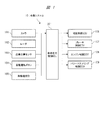
図1は、本実施の形態1による車載システム10の構成の一例を示すブロック図である。
<Configuration example of in-vehicle system>
FIG. 1 is a block diagram showing an example of the configuration of an in-
車載システム10は、例えば車両の自律走行を制御するシステムである。この車載システム10は、図1に示すように、カメラ101、レーダ102、自車位置センサ103、自動運転ボタン104、無線通信部105、補助制御ECU(Electronic Control Unit)106、ブレーキ制御ECU、エンジン制御ECU108、パワーステアリング制御ECU109、および自律走行制御ECU201を備える。
The in-
カメラ101、レーダ102、および自車位置センサ103は、車両の外界状況を認識する外界認識センサである。カメラ101およびレーダ102は、外界の認識や対象物までの距離を求めるセンサである。
The
自車位置センサ103は、GPS(Global Positioning System)などによって自車位置を検出するセンサである。自動運転ボタン104は、自動運転制御を開始したり、あるいは自動運転モードを変更したりするためのボタンである。通信装置である無線通信部105は、例えばOTA(Over-The-Air)により車載システムを更新するための、図示しない無線ネットワークに接続される。
The host
電子制御装置および自律走行制御装置である自律走行制御ECU201は、自動運転の車両走行制御装置である。補助制御ECU106は、補助の自動運転車両走行制御装置である。ブレーキ制御ECU107は、車両のブレーキ制御、すなわち制動力制御を行う制御装置である。
An autonomous
エンジン制御ECU108は、車両の駆動力を発生するエンジンを制御する制御装置である。パワーステアリング制御ECU109は、車両のパワーステアリングを制御する制御装置である。
The
カメラ101、レーダ102、自車位置センサ103、自動運転ボタン104、および無線通信部105は、自律走行制御ECU201にそれぞれ接続されている。自律走行制御ECU201には、これらカメラ101、レーダ102、自車位置センサ103からのセンサ情報や、自動運転ボタン104からの自動運転制御信号、および無線通信部105からの自律走行制御処理情報を含む更新情報などが伝達される。
The
また、自律走行制御ECU201、補助制御ECU106、ブレーキ制御ECU107、エンジン制御ECU108、およびパワーステアリング制御ECU109は、例えばCAN(Controller Area Network)によって相互に通信可能に接続される。
The autonomous
自律走行制御ECU201は、自動運転ボタン104により自動運転の開始要求を受け付けると、カメラ101、レーダ102、および自車位置センサ103など外界の情報に基づいて、車両の移動ルートを算出する。
When the autonomous
また、自律走行制御ECU201は、前述したルート通りに車両を移動させるように、ブレーキや駆動力などの制御指令をブレーキ制御ECU107、エンジン制御ECU108、およびパワーステアリング制御ECU109に出力する。
Further, the autonomous
ブレーキ制御ECU107、エンジン制御ECU108、およびパワーステアリング制御ECU109は、自律走行制御ECU201から自律走行制御の制御指令を受けて、例えばアクチュエータなどの各制御対象に操作信号を出力する。
The
つまり、自律走行制御ECU201は、制御指令を出力するメイン制御装置であり、ブレーキ制御ECU107、エンジン制御ECU108、およびパワーステアリング制御ECU109は、自律走行制御ECU201からの制御指令に応じて制御対象を制御するサブ制御装置である。
That is, the autonomous
なお、補助制御ECU106は、自律走行制御ECU201が異常の際に、該自律走行制御ECU201に代わって自動運転制御を行うための補助制御装置である。
The
〈自律走行制御ECUについて〉
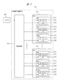
図2は、図1の車載システム10が有する自律走行制御ECU201における構成の一例を示すブロック図である。
<About the autonomous traveling control ECU>
FIG. 2 is a block diagram showing an example of the configuration of the autonomous
自律走行制御ECU201は、図2に示すように電源回路210、および複数のSoC211を備える。電源装置である電源回路210は、複数のSoC211に電源供給する。言い換えれば、複数のSoC211に電力を供給する。
The autonomous
SoC211は、CPU212、GPU213、およびFPGA214をそれぞれ有している。CPU212は、コアの論理回路であるコアロジック215および論理回路である入出力回路216を有する。
The
GPU213についても同様に、コアの論理回路であるコアロジック217および入出力回路218を有しており、FPGA214は、コアの論理回路であるコアロジック219および入出力回路220を有する。これらコアロジック215,217,219および入出力回路216,218,220は、論理回路からなる。
Similarly, the
ここでは、説明を簡略にするため、メモリや通信器などは省略する。これらのコアロジック215,217,219は、自動運転の認識、予測および制御の各アルゴリズムの演算などを実行する。 Here, in order to simplify the description, memories, communication devices and the like are omitted. These core logics 215, 217, 219 execute operations of automatic operation recognition, prediction and control algorithms, and the like.
入出力回路216,218,220は、各コアロジック215,217,219の間の情報のやりとりなどを行う。コアロジック215,217,219にて行われる演算負荷、各入出力回路216,218,220の通信頻度はそれぞれ異なるため、これらに供給される電源への要件は多種多様である。
The input /
多チャネルの電源回路210は、バッテリ300から供給される電源をコアロジック215,217,219や入出力回路216,218,220の電源要件に合うように変換して、それぞれ供給する。
The multi-channel
この図2では、1つのバッテリ300、および1つの電源回路210にて構成される例について説明したが、フェールオペレーションの観点から、それぞれを冗長構成にしてもよい。具体的には、冗長化された複数のSoCにそれぞれ電源回路とバッテリとを個別に用いて電源を供給してもよい。
Although FIG. 2 illustrates an example in which one
また、ここで説明したSoCの個数やその中の論理回路の構成などは一例である。これらは自律走行制御ECU201での演算規模に依存する。例えば、自律走行制御ECU201がカバーする自動運転レベルが高くなればなるほど、SoCの個数は増えて、その中の論理回路、すなわちコアロジックの構成も複雑になる。
In addition, the number of SoCs described here, the configuration of the logic circuit therein, and the like are examples. These depend on the calculation scale in the autonomous
〈電源回路の構成例〉
図3は、図2の自律走行制御ECU201が有する電源回路210における構成の一例を示す説明図である。
<Configuration Example of Power Supply Circuit>
FIG. 3 is an explanatory drawing showing an example of the configuration of the
電源回路210は、バッテリ300からの電源を負荷21−1〜21−Nにそれぞれ供給する。ここで、負荷21−1〜21−Nは、図2のコアロジック215,217,219および入出力回路216,218,220などに相当する。以下、負荷21−1〜21−Nを総称する場合には、単に負荷21と記載するものとする。
The
電源回路210は、スイッチング回路22−1〜22−N、コイル23−1〜23−N、コンデンサ24−1〜24−N、遷移管理部25、クロック生成部26、および管理データベース27を備える。
The
以下、スイッチング回路22−1〜22−Nを総称する場合には、単にスイッチング回路22と記載し、コイル23−1〜23−Nを総称する場合には、単にコイル23と記載する。また、コンデンサ24−1〜24−Nを総称する場合には、単にコンデンサ24と記載する。
Hereinafter, the switching circuits 22-1 to 22-N will be referred to simply as the switching
ここでは、スイッチング回路22がPWM(Pulse Width Modulation)制御方式を用いた降圧スイッチング回路を例にとり説明する。
Here, the step-down switching circuit in which the
クロック生成部26は、クロック信号を生成する。このクロック信号は、スイッチング回路22が有するスイッチのON/OFFを切り替える制御信号のベースとなる。クロック信号の周波数は、スイッチング周波数と呼ばれ、スイッチング回路22の電力効率、応答性などの特性はこのスイッチング周波数に依存する。
The
前述した通り、これらの特性への要求値は負荷21毎に異なるため、クロック生成部26は、複数の異なる周波数を生成する。遷移管理部25は、これらのクロック信号と観測された各負荷21への出力電圧Vout1、Vout2、・・・、VoutNにより、管理データベース27に格納された制御情報に基づいて、各スイッチング回路22に送信する制御信号C1、C2、・・・、CNを生成する。これら制御信号C1、C2、・・・、CNは、スイッチング信号である。
As described above, since the required values for these characteristics are different for each
ここでも、負荷への出力電圧Vout1、Vout2、・・・、VoutNを総称する場合には、単に出力電圧Voutと記載する。また、スイッチング回路に送信する制御信号C1、C2、・・・、CNを総称する場合には、単に制御信号Cと記載する。
Here, when the output voltages Vout1, Vout2,..., VoutN to the load are collectively referred to, they are simply described as the output voltage Vout. Also, when the control signals
制御信号Cは1(high)か0(low)の1ビットの信号としてよく、それぞれスイッチをON、OFFさせるための信号となる。遷移管理部25および管理データベース27の詳細については後述する。
The control signal C may be a 1-bit signal of 1 (high) or 0 (low), and is a signal for turning on / off the switch. Details of the
スイッチング回路22は、前述の制御信号Cにしたがって内部のスイッチをON/OFFさせることによりコイル23に流れるインダクタ電流を増減させる。負荷21に流れる出力電流により発生した出力電圧は、インダクタ電流の変動により大きなリップルを持つため、コンデンサ24を入れて平滑化して直流に近い電圧にしている。
The switching
ここで、入力電流Iin1〜IinNは、スイッチング回路22−1〜22−Nへの入力電流であり、該入力電流Iin1〜IinNを総称する場合には、単に入力電流Iinと記載する。 Here, the input currents Iin1 to IinN are input currents to the switching circuits 22-1 to 22-N. When the input currents Iin1 to IinN are collectively referred to, they are simply described as the input current Iin.
入力電流Iinと電源回路210の入力電流である入力電流IinSとには、以下の関係がある。
The following relation exists between the input current Iin and the input current IinS which is the input current of the

〈スイッチング回路の構成例〉
図4は、図3のスイッチング回路22における回路の一例を示す説明図である。図5は、図4のスイッチング回路22の他の回路例を示す説明図である。
<Configuration Example of Switching Circuit>
FIG. 4 is an explanatory view showing an example of a circuit in the switching
図4および図5は、いずれも降圧型のスイッチング回路の例を示している。降圧型のスイッチング回路は、直流の入力電圧をスイッチによって時間分割し、図示しないコイルおよびコンデンサによって平滑化することで所望のDC(直流)出力電圧にする。 4 and 5 each show an example of a step-down switching circuit. In the step-down switching circuit, a direct current input voltage is time-divided by a switch and smoothed by a coil and a capacitor (not shown) to obtain a desired DC (direct current) output voltage.
図4に示すスイッチング回路22は、同期型の降圧スイッチング回路であり、スイッチ41,43を有する。これらのスイッチ41,43は、制御信号C1H、C1LによりON/OFFがそれぞれ切り替えられる。制御信号C1H、C1Lは、例えば図3の遷移管理部25から出力される。理想的には、スイッチ41とスイッチ43とは、ON、OFFの状態が反転となる。
The switching
図5に示すスイッチング回路22は、非同期型の降圧スイッチング回路の例を示しており、スイッチ41およびダイオード42を有する。図4に示した同期型のスイッチング回路に比べて、基準電位であるグランドに接続されたスイッチがダイオード42に置き換わっているところが異なるが、基本的な動作は同じである。スイッチング回路22において、スイッチ41は、制御信号C1によりON/OFFが切り替わる。制御信号C1は、例えば図3の遷移管理部25から出力される。
The switching
以降、スイッチング回路22の構成は、図5の非同期型の降圧スイッチング回路であることを前提に説明する。図4の同期型の降圧スイッチング回路を用いる場合は、上述したように2つの制御信号C1H,C1Lが必要であるので、いずれかの制御信号を1つ追加する必要がある。追加する制御信号は、デッドタイムを考慮して元の制御信号を反転させて生成させてもよい。
Hereinafter, the configuration of the switching
〈遷移管理部の構成例〉
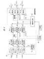
図6は、図3の電源回路210が有する遷移管理部25における一例を示すブロック図である。
<Configuration Example of Transition Management Unit>
FIG. 6 is a block diagram showing an example of the
ここでは、簡略化のため3個の電源チャネル用の遷移管理部25として説明する。
Here, the
遷移管理部25は、図6に示すように、レベルシフト部51−1〜51−3、出力誤差検出部52−1〜52−3、制御信号生成部53−1〜53−3、遅延部54−1〜54−3、基準電圧生成部55、および遷移判定部56を備える。
As shown in FIG. 6, the
以下、レベルシフト部51−1〜51−3を総称する場合は、レベルシフト部51と記載し、出力誤差検出部52−1〜52−3を総称する場合は、出力誤差検出部52と記載する。また、制御信号生成部53−1〜53−3を総称する場合は、制御信号生成部53と記載し、遅延部54−1〜54−3を総称する場合は、遅延部54と記載する。 Hereinafter, when the level shift units 51-1 to 51-3 are generically referred to, the level shift unit 51 is described, and when the output error detection units 52-1 to 52-3 are generically described, the output error detection unit 52 Do. The control signal generation units 53-1 to 53-3 are generally referred to as the control signal generation unit 53. The delay units 54-1 to 54-3 are generally referred to as the delay unit 54.
また、レベルシフト部51、出力誤差検出部52、制御信号生成部53、および基準電圧生成部55によって、出力電圧補正部が構成される。 Further, the level shift unit 51, the output error detection unit 52, the control signal generation unit 53, and the reference voltage generation unit 55 constitute an output voltage correction unit.
レベルシフト部51は、負荷への出力電圧Voutを基準電圧Vrefとコンパラブルになるように電圧変換する。レベルシフト部51は、変換した電圧を出力誤差検出部52に出力する。基準電圧生成部55は、基準電圧Vrefを生成する。 The level shift unit 51 converts the output voltage Vout to the load so as to be comparable to the reference voltage Vref. The level shift unit 51 outputs the converted voltage to the output error detection unit 52. The reference voltage generation unit 55 generates a reference voltage Vref.
出力誤差検出部52は、レベルシフト部51から出力される電圧と基準電圧生成部55が生成する基準電圧Vrefとの差分を出力する。制御信号生成部53は、クロック生成部26から入力された三角波と出力誤差検出部52から出力される差分から中間制御信号C’を生成する。中間制御信号C’は、PWM信号である。また、制御信号生成部53−1,53−2,53−3から出力される中間制御信号は、それぞれ中間制御信号C1’,C2’,C3’とする。
The output error detection unit 52 outputs the difference between the voltage output from the level shift unit 51 and the reference voltage Vref generated by the reference voltage generation unit 55. The control signal generation unit 53 generates an intermediate control signal C ′ from the triangular wave input from the
中間制御信号C’は、1(high)か0(low)かの1ビットの信号としてよく、それぞれスイッチをON、OFFさせるための信号となる。ここでは、例としてクロック生成部26から制御信号生成部53−1、53−2、53−3に入力される三角波の周期Tp1,Tp2,Tp3をそれぞれ時間T,2T,4Tとした。
The intermediate control signal C ′ may be a 1-bit signal of 1 (high) or 0 (low), and is a signal for turning on and off the switch, respectively. Here, as an example, periods Tp1, Tp2, and Tp3 of the triangular wave input from the
これらの逆数であるスイッチング周波数は、高くなればスイッチング損失が増え電源効率は下がるが、負荷変動に対する応答性は上がり、低くなれば、その逆になる。例えば、上記において、Tp1=Tの電源チャネルは、消費電流が比較的小さいが、動作周波数が比較的高く負荷変動が大きいCPUを想定する。 The switching frequency, which is the reciprocal of these, increases the switching loss and lowers the power supply efficiency if it is high, but the response to load fluctuation is high, and the reverse is the case if it is low. For example, in the above, it is assumed that the power supply channel of Tp1 = T has a relatively small consumption current but has a relatively high operating frequency and a large load fluctuation.
Tp3=4Tの電源チャネルは、消費電流が比較的大きく、動作周波数が比較的低く負荷変動が小さいFPGAを想定する。Tp2=2Tの電源チャネルは、これらの中間であるGPUを想定する。 The Tp3 = 4T power supply channel assumes an FPGA with relatively high current consumption, relatively low operating frequency, and low load fluctuation. The power supply channel of Tp2 = 2T assumes the GPU which is in between these.
遷移判定部56は、クロック生成部26からのタイミング信号、すなわち周期Ts=T/10をトリガにして、中間制御信号C’をサンプリングする。このタイミング信号が計測タイミング信号となる。
The
そして、サンプリングされた各信号を用いて演算処理することにより、各電源チャネルの必要遅延量を導出して、遅延部54に指令信号を送る。遷移判定部56による遷移判定に関する詳細は、後述する。
Then, the required delay amount of each power supply channel is derived by performing arithmetic processing using each sampled signal, and a command signal is sent to the delay unit 54. Details of the transition determination by the
ここでは、遷移判定部56の演算処理の結果、遅延部54−1,54−2,54−3への遅延量の指令信号は、それぞれTd1=0、Td2=3Ts、Td3=5Tsになったとして説明を進める。
Here, as a result of the arithmetic processing of the
遅延部54は、遷移判定部56からの遅延量の指令信号を受けて、それに合わせて中間制御信号C’を遅延させる。その結果、遅延部54−1,54−2,54−3は、制御信号C1(=C1’)、C2(=C2’+3Ts)、C3(=C3’+5Ts)を出力するに至る。
The delay unit 54 receives the command signal of the delay amount from the
〈遷移判定処理について〉
図7は、図6の遷移管理部25が実行する遷移判定処理の一例を示すフローチャートである。
<About transition determination processing>
FIG. 7 is a flowchart showing an example of the transition determination process performed by the
遷移判定処理は、電源回路210の入力電流IinSの電流リップルを低減する処理である。ここでは、遷移管理部25が伝導ノイズの瞬間値を検出する例を示す。また、図5と同様に、簡略化のため、遷移管理部25は、3個の電源チャネル用であるものとして説明する。
The transition determination process is a process of reducing the current ripple of the input current IinS of the
まず、遷移管理部25は、遷移判定処理を開始すると、該遷移管理部25が有する内部のカウンタ値tを0に更新し、設定された動作モードの制御情報を管理データベース27から読み込む(ステップS101)。この管理データベース27の詳細については後述する。
First, when the
続いて、クロック生成部26から出力されるタイミング信号を受け取るまで待機する(ステップS102)。そして、タイミング信号を受け取ったら、カウンタ値tをインクリメントし、各電源チャネルの中間制御信号C1’,C2’,C3’をタイミング信号に合わせてサンプリングしたC1’(t),C2’(t),C3’(t)を取得する(ステップS103)。
Subsequently, the process waits until the timing signal output from the
その後、これらのサンプリング値に基づいて、スイッチング回路22−1,22−2,22−3の入力電流のサンプリング値である電流Iin1(t),Iin2(t),Iin3(t)、電源回路の入力電流IinS(t)、およびこれらの時間当たりの変化量ΔIin1(t),ΔIin2(t),ΔIin3(t),ΔIinS(t)を下記の式2〜式5にしたがって計算する(ステップS104)。
Thereafter, based on these sampling values, currents Iin1 (t), Iin2 (t), Iin3 (t) which are sampling values of the input current of the switching circuits 22-1, 22-2, 22-3, The input current IinS (t), and the variation per time ΔIin1 (t), ΔIin2 (t), ΔIin3 (t), ΔIinS (t) are calculated according to the following
ここで、ImNは、管理データベース27から読み取った制御情報の1つである電流係数である。
Here, ImN is a current coefficient which is one of the control information read from the
![]()
![]()
小さい場合は、後述するステップS109の処理に進み、大きい場合は、ステップS106の処理において、|ΔIinS(t)|がΔIthを下回るように処理を行う。 If smaller, the process proceeds to the process of step S109 described later, and if larger, the process of step S106 is performed such that | ΔIinS (t) | falls below ΔIth.
具体的には、管理データベース27から読み取った制御情報の1つである優先順位情報により、優先順位の高い電源チャネルのΔIinN(t)を、ΔIinS(t)から減算する。
Specifically, ΔIinN (t) of the power supply channel with high priority is subtracted from ΔIinS (t) according to the priority information which is one of the control information read from the
そして、その減算結果をΔIinS(t)に置き換え、下記の式が成立するまで同様の減算を繰り返す(ステップS106)。ここでは、優先順位にしたがって減算したが、|ΔIinN(t)|が大きい電源チャネルから減算してもよい。 Then, the subtraction result is replaced with ΔIinS (t), and the same subtraction is repeated until the following equation is established (step S106). Here, although subtraction is performed according to the priority, it may be subtracted from a power supply channel in which | ΔIinN (t) | is large.
![]()
![]()
一方、成立する場合には、減算した電源チャネルについて、管理データベース27から読み取った制御情報の1つである遅延量TdNだけ遅延させるように、遅延部54に指令信号を送る(ステップS108)。 On the other hand, when the condition is satisfied, a command signal is sent to the delay unit 54 so as to delay the power supply channel thus subtracted by the delay amount TdN which is one of the control information read from the management database 27 (step S108).
最後に、この一連の処理フローの間に、上位システムからの動作モードの切り替え指令の有無を確認する(ステップS109)。切り替え指令がありの場合には、本処理を終了し、なしの場合には、ステップS102の処理に戻って本処理を継続する。 Finally, during this series of processing flow, it is checked whether or not there is an operation mode switching command from the host system (step S109). If there is a switching instruction, the present process is ended. If not, the process returns to step S102 to continue the present process.
ここでは、伝導ノイズの瞬間値を検出する例を示したが、時間平均値を検出する場合も類似の手法が適用可能である。例えば、上述したΔIinN(t)やΔIinS(t)を、サンプル数一定としたカウンタ値tまでの時間平均値に置き換えてもよい。 Although the example which detects the instantaneous value of conduction noise was shown here, the same technique is applicable also when detecting a time average value. For example, the above-described ΔIinN (t) and ΔIinS (t) may be replaced with the time average value up to the counter value t, where the number of samples is fixed.
〈管理データベースの構成例〉
図8は、図3の電源回路210が有する管理データベース27におけるデータ構成の一例を示す説明図である。
<Configuration example of management database>
FIG. 8 is an explanatory view showing an example of the data configuration in the
管理データベース27は、動作モード72と該当モードの遷移判定処理のパラメータである制御情報73−1〜制御情報73−6とが対応付けされている。ここで、制御情報73−1〜制御情報73−6を総称する場合には、単に制御情報73と記載する。管理データベース27は、遷移管理部25によって参照される。
In the
ここでは、動作モード72は、自動運転における適用例を示しており、例えば市街地走行モードであるモードA、高速道路走行モードであるモードB、駐車モードであるモードC、およびECUの異常検出時のモードであるモードDとしている。
Here, the
これら動作モード72に対応する制御情報73において、制御情報73−1には伝導ノイズの検出モード情報が格納されている。この場合、制御情報73−1は、通常動作時、すなわちモードA〜Cでは、瞬間値検出と平均値検出とを行うが、モードECU異常、すなわちモードDの緊急時には、瞬間値検出のみを実施する設定となる。
In the control information 73 corresponding to the
制御情報73−2には、例えば中間制御情報C’をサンプリングするタイムスパンTsの情報が格納されている。より高精度な検出をするために、動作モードに応じてタイムスパンを小さくしてもよいし、あるいはより低遅延な演算処理をするためにタイムスパンを大きく設定するようにしてもよい。 The control information 73-2 stores, for example, information of a time span Ts for sampling the intermediate control information C '. In order to perform detection with higher accuracy, the time span may be reduced according to the operation mode, or the time span may be set larger to perform calculation processing with lower delay.
タイムスパンを可変とする場合は、クロック生成部26にそれに合わせたクロックを生成するように指令信号を出力して制御してもよい。あるいは予めクロック生成部26に短周期のタイミング信号を生成させておき、遷移判定部56にて適宜間引いて使用してもよい。
When the time span is variable, a command signal may be output and controlled so as to generate a clock according to the
制御情報73−3には、電流変動しきい値ΔIthの情報が格納されている。瞬間値検出と平均値検出でそれぞれ電流変動しきい値をΔIthpk、ΔIthavと分けて設定してもよい。これらの数値は、例えば伝導ノイズの標準規格値を参考に設定する。 The control information 73-3 stores information of the current fluctuation threshold ΔIth. The current variation threshold may be set separately for ΔIthpk and ΔIthav in instantaneous value detection and average value detection. These numerical values are set, for example, with reference to a standard value of conducted noise.
制御情報73−4には、各スイッチング回路22の入力電流を計算する電流係数Im1〜ImNの情報が格納される。この電流係数Im1〜ImNは、例えば各スイッチング回路22に接続される負荷に流れる最大電流をシミュレーションや実測により予め導出しておき、それに基づいて設定される。
The control information 73-4 stores information of current coefficients Im1 to ImN for calculating the input current of each switching
制御情報73−5には、各電源チャネルに対応した遅延量Td1〜TdNの情報が格納されている。遷移管理部25は、この情報に応じて遅延部54に遅延させる遅延量を決定する。
The control information 73-5 stores information on delay amounts Td1 to TdN corresponding to the respective power supply channels. The
制御情報73−6には、各電源チャネルの遷移管理の優先順位に関する情報が格納されている。ここでの優先順位が高いものほど、遅延させる優先度が高くなる。言い換えれば高信頼な演算を司るコアロジックなどに電源供給する電源チャネルは、優先度が低く設定される。 The control information 73-6 stores information on the priority of transition management of each power supply channel. The higher the priority here, the higher the priority to be delayed. In other words, the power supply channel for supplying power to core logic and the like responsible for highly reliable operation is set to have a low priority.
このように、動作モードに応じて遷移判定処理を変更してもよい。管理データベース27は、例えば、クラウド上のサーバなどからOTAにより無線ネットワーク経由で自動運転の動作モードや制御情報を追加変更してもよい。
Thus, the transition determination process may be changed according to the operation mode. For example, the
はじめに、サーバにデータベース追加の指示が設定されると、更新データが図1の車載システム10の無線通信部105に転送される。無線通信部105は、受信した更新データを自律走行制御ECU201の遷移管理部25に転送する。これにより、自動運転の動作モードや制御情報など追加変更の処理が完了する。
First, when an instruction to add a database is set to the server, the update data is transferred to the
これにより、自動運転の動作モードに求められる演算負荷、例えば性能や遅延などに応じて柔軟に遷移判定処理を再設定させることができる。さらに、新しい自動運転の動作モードを追加する場合などにおいても、利用中の動作モードには影響を与えることなく、その追加する動作モードにて利用する遷移管理情報を電源回路210に追加導入することができる。
Thus, it is possible to flexibly reset the transition determination processing according to the operation load required for the operation mode of the automatic driving, for example, the performance or the delay. Furthermore, even when adding a new operation mode of automatic operation, etc., transition control information used in the added operation mode is additionally introduced into the
例えば車両の周辺環境あるいは図2のSoC211の演算処理に応じて、制御情報73−3の電流変動しきい値ΔIthを設定するようにしてもよい。具体的には、市街地走行モードであるモードAにおいて、市街地走行が行われる場合に、道路の混雑状況、例えば渋滞時かあるいは渋滞していないかなどの状況に応じて電流変動しきい値ΔIthを設定する。これは、高速道路走行モードであるモードBにおいても同様である。これにより、より緻密に制御信号Cを生成することができ、入力電流の伝導ノイズを精度よく低減することができる。
For example, the current variation threshold value ΔIth of the control information 73-3 may be set according to the peripheral environment of the vehicle or the calculation process of the
〈効果〉
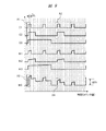
続いて、図9および図10を用いて効果を説明する。
<effect>
Subsequently, the effects will be described using FIGS. 9 and 10.
図9は、本発明者の検討による電源回路における各信号波形の一例を示す模式図である。 FIG. 9 is a schematic view showing an example of each signal waveform in the power supply circuit examined by the present inventor.
この図9は、図7などに示した遷移判定処理による遅延制御の機能を有していない遷移管理部による例を示しており、上方から下方にかけて、遷移管理部から出力される制御信号C1〜C3、スイッチング回路への入力電流Iin1〜Iin3、および電源回路の入力電流IinSの各波形の信号タイミングをそれぞれ示している。また、横軸は、図7にて説明したタイミング信号である。 FIG. 9 shows an example by the transition management unit not having the delay control function by the transition determination processing shown in FIG. 7 etc., and control signals C1 to C1 output from the transition management unit from top to bottom are shown. Signal timings of waveforms of C3, input currents Iin1 to Iin3 to the switching circuit, and input current IinS of the power supply circuit are shown. The horizontal axis is the timing signal described in FIG.
この場合、図6において説明したとおり、各制御信号の周期Tp1,Tp2,Tp3は、それぞれT,2T,4Tとし、また、クロック生成部26からのタイミング信号の周期Tsは、T/10としている。
In this case, as described in FIG. 6, the periods Tp1, Tp2 and Tp3 of the control signals are T, 2T and 4T, respectively, and the period Ts of the timing signal from the
各制御信号C1〜C3によってスイッチング回路への入力電流は、Iin1〜Iin3のような挙動を示し、その総和である電源回路への入力電流波形はIinSのようになる。 The input current to the switching circuit behaves like Iin1 to Iin3 according to each control signal C1 to C3, and the input current waveform to the power supply circuit, which is the sum thereof, becomes like IinS.
ここで、図9に示すポイントA1(t=2〜3)において、制御信号C1,C2,C3は、同時にlowからhighに立ち上がっており、この結果、IinSは、ポイントA3において、伝導ノイズ標準規格値を参考に設定した電流変動しきい値ΔIthよりも大きなΔIinS(3)を持つ。 Here, at points A1 (t = 2 to 3) shown in FIG. 9, the control signals C1, C2 and C3 simultaneously rise from low to high, and as a result, IinS is a conducted noise standard at point A3. It has ΔIinS (3) larger than the current fluctuation threshold ΔIth set based on the value.
また、図9のポイントA2においても、制御信号C1と制御信号C2とが同時に立ち上がっていることが見て取れる。これにより、ポイントA4にて発生する伝導ノイズは、ポイントA3の伝導ノイズに比べて小さいため、まずはポイントA3の伝導ノイズを低減することが最優先事項である。 Also, at point A2 in FIG. 9, it can be seen that the control signal C1 and the control signal C2 are simultaneously rising. Thereby, since the conduction noise generated at the point A4 is smaller than the conduction noise at the point A3, it is a top priority to reduce the conduction noise at the point A3 first.
図10は、図6に示す遷移管理部25が有する電源回路210における各信号波形の一例を示す模式図である。
FIG. 10 is a schematic view showing an example of each signal waveform in the
図10においても、上方から下方にかけては、遷移管理部25から出力される制御信号C1〜C3、スイッチング回路22への入力電流Iin1〜Iin3、および電源回路210の入力電流IinSの各波形の信号タイミングをそれぞれ示している。また、横軸は、図7にて説明したタイミング信号である。
Also in FIG. 10, from the top to the bottom, the signal timings of the control signals C1 to C3 output from the
この場合、図6および図7などにて説明した遷移判定処理により、ΔIinS(3)が電流変動しきい値ΔIthを超えないように、制御信号C2,C3の制御信号を図9に比べて、それぞれ3Ts,5Ts遅延させている。 In this case, the control signals of control signals C2 and C3 are compared with those in FIG. 9 so that .DELTA.IinS (3) does not exceed current variation threshold value .DELTA.Ith by the transition determination processing described in FIGS. They are delayed by 3Ts and 5Ts respectively.
その結果、図9におけるポイントA3でのΔIinS(3)は、図10におけるポイントB3に示す通り、大きく低減されておりΔIthよりも下回る。逆に、図10のポイントB4におけるΔIinSの方がポイントB3のそれよりも大きくなるが、ΔIthよりは小さく収まる。 As a result, ΔIinS (3) at point A3 in FIG. 9 is greatly reduced and falls below ΔIth, as shown at point B3 in FIG. Conversely, ΔIinS at point B4 in FIG. 10 is larger than that at point B3, but smaller than ΔIth.
本実施の形態に示した例では、2つのスイッチング回路のスイッチング周波数の整数倍となるように三つ目のスイッチング回路のスイッチング周波数を選定しているため、遅延制御を一度行うだけで、それ以降の遅延制御をほぼ行う必要がない。また、ここでは、3つのスイッチング回路のスイッチング周波数を全て異ならせたが、1つだけ異ならせるだけでも本実施の形態に近い効果が得られる。 In the example shown in the present embodiment, the switching frequency of the third switching circuit is selected to be an integral multiple of the switching frequency of the two switching circuits. There is almost no need to perform delay control of Further, although the switching frequencies of the three switching circuits are all different here, the effect similar to that of the present embodiment can be obtained by changing only one.
このように、複数のスイッチング回路22の入力電流の変化量の合計値に基づいて、制御信号の遅延量を制御することにより、多数の電源チャネルを持つ自動運転向けのなど制御装置においても、入力電流の伝導ノイズを効果的に低減することができる。
As described above, by controlling the delay amount of the control signal based on the total value of the change amounts of the input currents of the plurality of switching
その結果、信頼性の高い電子制御装置、すなわち自律走行制御ECU201を提供することができる。また、大容量の入力コンデンサなどが不要となるので、自律走行制御ECU201の小型化および低コスト化を実現することができる。
As a result, it is possible to provide a highly reliable electronic control device, that is, the autonomous
(実施の形態2)
前記実施の形態1では、遷移管理部25が制御信号の遅延を動的に制御して、伝導ノイズを低減させていたが、本実施の形態2においては、静的な制御をする技術について説明する。
Second Embodiment
In the first embodiment, the
〈遷移管理部の構成例〉
図11は、本実施の形態2による遷移管理部25における構成の一例を示す説明図である。
<Configuration Example of Transition Management Unit>
FIG. 11 is an explanatory drawing showing an example of the configuration of the
以下、図11を用いて、前記実施の形態1と大きく異なる遷移管理部25を中心に説明する。ここでは、遷移管理部25は、簡略化のため3個の電源チャネル用の遷移判定処理を行うものとして説明する。
Hereinafter, the
遷移管理部25は、図11に示すように、レベルシフト部51−1〜51−3、出力誤差検出部52−1〜52−3、制御信号生成部53−1〜53−3、遅延部54−1〜54−3、および基準電圧生成部55を備える。図11の遷移管理部25が前記実施の形態1の図6の遷移管理部25と異なるところは、遷移判定部56が設けられていない点である。
As illustrated in FIG. 11, the
以下、レベルシフト部51−1〜51−3を総称する場合には、単にレベルシフト部51と記載し、出力誤差検出部52−1〜52−3を総称する場合には、単に出力誤差検出部52と記載する。 Hereinafter, when the level shift units 51-1 to 51-3 are collectively referred to, they are simply described as the level shift unit 51, and when the output error detection units 52-1 to 52-3 are collectively referred to, the output error detection is simply performed. It describes as the part 52.
また、制御信号生成部53−1〜53−3を総称する場合には、単に制御信号生成部53と記載し、遅延部54−1〜54−3を総称する場合には、単に遅延部54と記載する。 When the control signal generation units 53-1 to 53-3 are collectively referred to, they are simply referred to as the control signal generation unit 53. When the delay units 54-1 to 54-3 are collectively referred to, the delay unit 54 is simply referred to. And write.
レベルシフト部51は、負荷への出力電圧Voutを基準電圧Vrefとコンパラブルになるように電圧変換して、次段の出力誤差検出部52へ出力する。出力誤差検出部52は、レベルシフト部51からの入力電圧と基準電圧Vrefとの差分を出力する。基準電圧生成部55は、基準電圧Vrefを生成する。 The level shift unit 51 converts the output voltage Vout to the load so as to be comparable to the reference voltage Vref, and outputs the voltage to the output error detection unit 52 at the next stage. The output error detection unit 52 outputs the difference between the input voltage from the level shift unit 51 and the reference voltage Vref. The reference voltage generation unit 55 generates a reference voltage Vref.
制御信号生成部53は、クロック生成部26から入力された三角波と出力誤差検出部52から出力される差分からPWM信号である中間制御信号C1’、C2’、C3’を生成する。
The control signal generation unit 53 generates intermediate control signals C1 ', C2' and C3 'which are PWM signals from the triangular wave input from the
ここでは例として、クロック生成部26から制御信号生成部53−1、53−2、53−3に入力される三角波の周期Tp1、Tp2、Tp3はそれぞれT、2T、4Tとした。
Here, as an example, periods Tp1, Tp2, and Tp3 of the triangular wave input from the
遅延部54は、中間制御信号C1’,C2’,C3’を予め設定された遅延量Td1,Td2,Td3だけ遅延させて制御信号C1,C2,C3を出力する。遅延部54の遅延量は、予め設定されている。 The delay unit 54 delays the intermediate control signals C1 ', C2' and C3 'by preset delay amounts Td1, Td2 and Td3 and outputs control signals C1, C2 and C3. The delay amount of the delay unit 54 is preset.
この遅延量は、例えばスイッチング周波数を上記のように定めた時に各スイッチング回路の遅延量をどのように設定すれば伝導ノイズが許容値に収まるかどうかを予め実測もしくはシミュレーションすることによって導出して設定する。 For example, when the switching frequency is determined as described above, the delay amount is set by deriving or measuring in advance whether or not the conducted noise falls within the allowable value if the delay amount of each switching circuit is set. Do.
このように、遅延部54の遅延量が固定されているために、電源回路210には、管理データベース27が不要となる。よって、この場合、電源回路210は、前記実施の形態1の図3に示す構成から管理データベース27を除いた構成となる。
As described above, since the delay amount of the delay unit 54 is fixed, the
これによっても、前記実施の形態1の図10と同様の電流波形が得られる。その結果、伝導ノイズを小さく抑制することができる。本例では、3つのスイッチング回路のスイッチング周波数が全て異なるようにしたが、例えば1つのスイッチング周波数のみが異なるようにするだけでも良好に伝導ノイズを抑制する効果が得られる。 Also in this case, a current waveform similar to that of FIG. 10 of the first embodiment can be obtained. As a result, the conducted noise can be suppressed small. In this example, all the switching frequencies of the three switching circuits are made different, but for example, the effect of suppressing the conduction noise can be obtained well only by making only one switching frequency different.
以上により、管理データベース27および遷移判定部56を不要とすることができるので、自律走行制御ECU201をより低コストにすることができる。
As described above, since the
(実施の形態3)
前記実施の形態1では、スイッチング回路22の入力電流Iinを中間制御信号C’から推定する構成としていたが、本実施の形態3においては、入力電流Iinを直接計測して、高精度に伝導ノイズをコントロールする技術について説明する。
Third Embodiment
In the first embodiment, the input current Iin of the switching
〈電源回路の構成例〉
以下、図12および図13を用いて、前記実施の形態1と異なる電源回路および遷移管理部を中心に説明する。
<Configuration Example of Power Supply Circuit>
The power supply circuit and transition management unit different from the first embodiment will be mainly described below with reference to FIGS. 12 and 13.
図12は、本実施の形態3による電源回路210における構成の一例を示すブロック図である。
FIG. 12 is a block diagram showing an example of a configuration of the
図12の電源回路210において、図3の電源回路210と異なるところは、電流計測部である電流センサ28−1〜28−Nが新たに設けられた点である。電流センサ28−1〜28−Nを総称する場合は、単に電流センサ28と記載する。
The
電流センサ28−1〜28−Nは、スイッチング回路22−1〜22−Nの入力部それぞれ設けられており、入力電流Iin1〜IinNを計測する。 The current sensors 28-1 to 28-N are provided at the input portions of the switching circuits 22-1 to 22-N, respectively, and measure the input currents Iin1 to IinN.
これら電流センサ28が計測した計測結果は、遷移管理部25に送られて、後述する遷移判定処理に用いられる。なお、電流センサ28は、例えばカレントトランスやホール素子、あるいはGMR(Giant Magneto Resistive effect)素子などを用いた電流検出回路を用いるようにしてもよい。また、より高精度な電流計測を行う場合には、電源回路210の入力電流IinSを計測する電流センサを追加してもよい。
The measurement results measured by the
〈遷移管理部の構成例〉
図13は、図12の電源回路210が有する遷移管理部25における構成の一例を示す説明図である。
<Configuration Example of Transition Management Unit>
FIG. 13 is an explanatory diagram showing an example of a configuration of the
ここでは簡略化のため、遷移管理部25が3個の電源チャネル用の遷移判定処理を行うものとして説明する。
Here, for the sake of simplicity, it is assumed that the
遷移管理部25は、レベルシフト部51−1〜51−3、出力誤差検出部52−1〜52−3、制御信号生成部53−1〜53−3、遅延部54−1〜54−3、基準電圧生成部55、および遷移判定部56を備える。
The
レベルシフト部51は、負荷への出力電圧Voutを、基準電圧生成部55が生成する基準電圧Vrefとコンパラブルになるように電圧変換して、次段の出力誤差検出部52へ出力する。 The level shift unit 51 converts the output voltage Vout to the load so as to be comparable to the reference voltage Vref generated by the reference voltage generation unit 55, and outputs the converted voltage to the output error detection unit 52 of the next stage.
出力誤差検出部52は、レベルシフト部51から出力される電圧と基準電圧Vrefとの差分を出力する。制御信号生成部53は、クロック生成部26から入力された三角波と出力誤差検出部52から出力される差分からPWM信号である中間制御信号C1’、C2’、C3’を生成する。
The output error detection unit 52 outputs the difference between the voltage output from the level shift unit 51 and the reference voltage Vref. The control signal generation unit 53 generates intermediate control signals C1 ', C2' and C3 'which are PWM signals from the triangular wave input from the
ここでは例として、クロック生成部26から制御信号生成部53−1、53−2、53−3に入力される三角波の周期Tp1、Tp2、Tp3はそれぞれT、2T、4Tとした。
Here, as an example, periods Tp1, Tp2, and Tp3 of the triangular wave input from the
遷移判定部56は、クロック生成部26から出力されるタイミング信号(周期Ts=T/10)をトリガにして、電流センサ28で計測された入力電流Iinをサンプリングする。
The
そして、これらのサンプリング値を用いて演算処理することにより、各電源チャネルの必要遅延量を導出して遅延部54に指令信号を送る。ここでは、遷移判定部56の演算処理の結果、遅延部54−1,54−2,54−3への遅延量の指令信号は、それぞれTd1=0,Td2=3Ts,Td3=5Tsになったとしている。
Then, by performing arithmetic processing using these sampling values, the required delay amount of each power supply channel is derived and a command signal is sent to the delay unit 54. Here, as a result of the arithmetic processing of the
遅延部54は、遷移判定部56からの遅延量指令を受けて、それに合わせて中間制御信号C’を遅延させる。その結果、遅延部54−1,54−2,54−3は制御信号C1(=C1’),C2(=C2’+3Ts),C3(=C3’+5Ts)を出力する。
The delay unit 54 receives the delay amount command from the
以上により、スイッチング回路22の入力電流を電流センサ28によって計測し、その変化量の合計値に基づいて、制御信号の遅延量を予め設定することにより、多数の電源チャネルを持つ電子制御装置、すなわち自律走行制御ECU201においても、入力電流の伝導ノイズをより高精度にコントロールすることができる。
As described above, the input current of the switching
それにより、信頼性が高い自律走行制御ECU201を提供することができる。また、大容量の入力コンデンサなどを不要にすることができるので、自律走行制御ECU201のコストを削減でき、小型化を実現することができる。
Thereby, highly reliable autonomous traveling control ECU201 can be provided. In addition, since a large capacity input capacitor and the like can be eliminated, the cost of the autonomous
以上、本発明者によってなされた発明を実施の形態に基づき具体的に説明したが、本発明は前記実施の形態に限定されるものではなく、その要旨を逸脱しない範囲で種々変更可能であることはいうまでもない。 As mentioned above, although the invention made by the present inventor was concretely explained based on an embodiment, the present invention is not limited to the above-mentioned embodiment, and can be variously changed in the range which does not deviate from the gist. Needless to say.
なお、本発明は上記した実施の形態に限定されるものではなく、様々な変形例が含まれる。例えば、上記した実施の形態は本発明を分かりやすく説明するために詳細に説明したものであり、必ずしも説明した全ての構成を備えるものに限定されるものではない。 The present invention is not limited to the above-described embodiment, but includes various modifications. For example, the above-described embodiments are described in detail to explain the present invention in an easy-to-understand manner, and are not necessarily limited to those having all the described configurations.
また、ある実施の形態の構成の一部を他の実施の形態の構成に置き換えることが可能であり、また、ある実施の形態の構成に他の実施の形態の構成を加えることも可能である。また、各実施の形態の構成の一部について、他の構成の追加、削除、置換をすることが可能である。 Also, part of the configuration of one embodiment can be replaced with the configuration of another embodiment, and the configuration of another embodiment can be added to the configuration of one embodiment. . In addition, it is possible to add, delete, and replace other configurations in part of the configurations of the respective embodiments.
また、上記の各構成、機能、処理部、処理手段等は、それらの一部又は全部を、例えば集積回路で設計する等によりハードウェアで実現してもよい。また、上記の各構成、機能等は、プロセッサがそれぞれの機能を実現するプログラムを解釈し、実行することによりソフトウェアで実現してもよい。各機能を実現するプログラム、テーブル、ファイル等の情報は、メモリや、ハードディスク、SSD(Solid State Drive)等の記録装置、または、ICカード、SDカード、DVDなどの記録媒体に置くことができる。 Further, each of the configurations, functions, processing units, processing means, etc. described above may be realized by hardware, for example, by designing part or all of them with an integrated circuit. Further, each configuration, function, etc. described above may be realized by software by the processor interpreting and executing a program that realizes each function. Information such as a program, a table, and a file for realizing each function can be placed in a memory, a hard disk, a recording device such as a solid state drive (SSD), or a recording medium such as an IC card, an SD card, or a DVD.
また、制御線や情報線は説明上必要と考えられるものを示しており、製品上必ずしも全ての制御線や情報線を示しているとは限らない。実際には殆ど全ての構成が相互に接続されていると考えてもよい。 Further, control lines and information lines indicate what is considered to be necessary for the description, and not all control lines and information lines in the product are necessarily shown. In practice, almost all configurations may be considered to be mutually connected.
10 車載システム
21 負荷
22 スイッチング回路
23 コイル
24 コンデンサ
25 遷移管理部
26 クロック生成部
27 管理データベース
28 電流センサ
41 スイッチ
42 ダイオード
43 スイッチ
51 レベルシフト部
52 出力誤差検出部
53 制御信号生成部
54 遅延部
55 基準電圧生成部
56 遷移判定部
101 カメラ
102 レーダ
103 自車位置センサ
104 自動運転ボタン
105 無線通信部
106 補助制御ECU
107 ブレーキ制御ECU
108 エンジン制御ECU
109 パワーステアリング制御ECU
201 自律走行制御ECU
210 電源回路
215 コアロジック
216 入出力回路
217 コアロジック
218 入出力回路
219 コアロジック
220 入出力回路
300 バッテリ
DESCRIPTION OF
107 Brake control ECU
108 engine control ECU
109 Power steering control ECU
201 Autonomous travel control ECU
210
Claims (15)
前記電源装置は、
スイッチング信号に基づいて、複数の前記論理回路に供給する電源をそれぞれ生成して出力する複数のスイッチング回路と、
複数の前記スイッチング回路を制御する遷移管理部と、
複数のクロック信号を生成するクロック生成部と、
を有し、
前記遷移管理部は、
前記クロック生成部が生成する前記クロック信号から中間制御信号を生成する制御信号生成部と、
複数の前記スイッチング回路に対応してそれぞれ設けられ、指令信号に基づいて、前記中間制御信号を遅延させ、遅延させた前記中間制御信号を前記スイッチング信号として出力する複数の遅延部と、
を有し、
前記クロック生成部が生成する複数の前記クロック信号は、少なくとも1つのクロック信号が異なる周波数である、電子制御装置。 An electronic control device comprising: a plurality of logic circuits and a power supply device for supplying power to the plurality of logic circuits,
The power supply device
A plurality of switching circuits that respectively generate and output power supplies to the plurality of logic circuits based on a switching signal;
A transition management unit that controls a plurality of the switching circuits;
A clock generation unit that generates a plurality of clock signals;
Have
The transition management unit
A control signal generation unit that generates an intermediate control signal from the clock signal generated by the clock generation unit;
A plurality of delay units provided corresponding to the plurality of switching circuits, each delaying the intermediate control signal based on a command signal and outputting the delayed intermediate control signal as the switching signal;
Have
The electronic control device according to claim 1, wherein the plurality of clock signals generated by the clock generation unit have different frequencies at least one clock signal.
前記遷移管理部は、予め設定される制御情報に基づいて、前記指令信号を生成する遷移判定部を有し、
前記遷移判定部は、前記指令信号により、複数の前記スイッチング回路の入力電流の変化量の合計値を算出して、算出した前記合計値と予め設定された電流変動しきい値とを比較して、比較した前記合計値が前記電流変動しきい値以下となるように前記遅延部の遅延量を制御する、電子制御装置。 In the electronic control unit according to claim 1,
The transition management unit includes a transition determination unit that generates the command signal based on control information set in advance.
The transition determination unit calculates a total value of change amounts of input currents of the plurality of switching circuits according to the command signal, and compares the calculated total value with a preset current fluctuation threshold value. And an electronic control unit that controls the delay amount of the delay unit such that the compared total value becomes equal to or less than the current fluctuation threshold value.
前記遷移判定部は、前記制御信号生成部が生成する前記中間制御信号から複数の前記スイッチング回路の入力電流の変化量の合計値を算出する、電子制御装置。 In the electronic control unit according to claim 2,
The electronic control unit, wherein the transition determination unit calculates a total value of change amounts of input currents of the plurality of switching circuits from the intermediate control signal generated by the control signal generation unit.
前記電源装置は、複数の前記スイッチング回路に入力される入力電流を計測する電流計測部を有し、
前記遷移判定部は、前記電流計測部が計測した電流の計測結果から前記入力電流の変化量の合計値を算出する、電子制御装置。 In the electronic control unit according to claim 2,
The power supply device includes a current measurement unit that measures an input current input to the plurality of switching circuits,
The electronic control unit, wherein the transition determination unit calculates a total value of change amounts of the input current from measurement results of the current measured by the current measurement unit.
前記遷移判定部は、計測タイミング信号に同期して、前記入力電流の立ち上り/立ち下りの有無を判定し、その判定結果から前記入力電流の変化量の合計値を算出する、電子制御装置。 In the electronic control unit according to claim 2,
The electronic control unit according to claim 1, wherein the transition determination unit determines presence / absence of rising / falling of the input current in synchronization with a measurement timing signal, and calculates a total value of change amounts of the input current from the determination result.
前記遷移判定部が比較する前記電流変動しきい値は、前記電子制御装置の動作モード毎に異なる値である、電子制御装置。 In the electronic control unit according to claim 2,
The electronic control unit according to claim 1, wherein the current variation threshold value that the transition determination unit compares is a value that varies depending on the operation mode of the electronic control unit.
前記電源装置は、前記制御情報を格納する管理データベースを有し、
前記管理データベースは、前記入力電流を演算する際に用いる電流係数、複数の前記スイッチング回路にそれぞれ対応する遅延量、または遅延させる複数の前記スイッチング回路の優先順位の少なくともいずれか1つを格納し、
前記管理データベースに格納される前記電流係数、前記遅延量、または前記優先順位は、前記電子制御装置の動作モード毎にそれぞれ設定されている、電子制御装置。 In the in-vehicle system according to claim 2,
The power supply device has a management database storing the control information.
The management database stores at least one of a current coefficient used when computing the input current, a delay amount corresponding to each of the plurality of switching circuits, or a priority of the plurality of switching circuits to be delayed.
The electronic control device, wherein the current coefficient, the delay amount, or the priority stored in the management database is set for each operation mode of the electronic control device.
前記遷移管理部は、複数の前記スイッチング回路が生成する出力電圧の誤差をそれぞれ検出して、その検出結果に基づいて、前記出力電圧の誤差を減少させるように前記中間制御信号を補正する出力電圧補正部を有する、電子制御装置。 In the electronic control unit according to claim 2,
The transition management unit detects an error of the output voltage generated by the plurality of switching circuits, and corrects the intermediate control signal so as to reduce the error of the output voltage based on the detection result. An electronic control unit having a correction unit.
前記自律走行制御装置は、
複数の論理回路と、
複数の前記論理回路に電源を供給する電源装置と、
を備え、
前記電源装置は、
スイッチング信号に基づいて、複数の前記論理回路に供給する電源をそれぞれ生成して出力する複数のスイッチング回路と、
複数の前記スイッチング回路を制御する遷移管理部と、
複数のクロック信号を生成するクロック生成部と、
を有し、
前記遷移管理部は、
前記クロック生成部が生成する前記クロック信号から中間制御信号を生成する制御信号生成部と、
複数の前記スイッチング回路に対応してそれぞれ設けられ、指令信号に基づいて、前記中間制御信号を遅延させ、遅延させた前記中間制御信号を前記スイッチング信号として出力する複数の遅延部と、
を有し、
前記クロック生成部が生成する複数の前記クロック信号は、少なくとも1つのクロック信号が異なる周波数である、車載システム。 An on-vehicle system comprising an autonomous traveling control device for controlling autonomous traveling of a vehicle, comprising:
The autonomous traveling control device
With multiple logic circuits,
A power supply for supplying power to the plurality of logic circuits;
Equipped with
The power supply device
A plurality of switching circuits that respectively generate and output power supplies to the plurality of logic circuits based on a switching signal;
A transition management unit that controls a plurality of the switching circuits;
A clock generation unit that generates a plurality of clock signals;
Have
The transition management unit
A control signal generation unit that generates an intermediate control signal from the clock signal generated by the clock generation unit;
A plurality of delay units provided corresponding to the plurality of switching circuits, each delaying the intermediate control signal based on a command signal and outputting the delayed intermediate control signal as the switching signal;
Have
The in-vehicle system according to the present invention, wherein the plurality of clock signals generated by the clock generation unit have different frequencies of at least one clock signal.
前記遷移管理部は、予め設定される制御情報に基づいて、前記指令信号を生成する遷移判定部を有し、
前記遷移判定部は、前記指令信号により、複数の前記スイッチング回路の入力電流の変化量の合計値を算出して、算出した前記合計値と予め設定された電流変動しきい値とを比較して、比較した前記合計値が前記電流変動しきい値以下となるように前記遅延部の遅延量を制御する、車載システム。 In the in-vehicle system according to claim 9,
The transition management unit includes a transition determination unit that generates the command signal based on control information set in advance.
The transition determination unit calculates a total value of change amounts of input currents of the plurality of switching circuits according to the command signal, and compares the calculated total value with a preset current fluctuation threshold value. The on-vehicle system which controls the delay amount of the said delay part so that the said total value compared may become below the said current fluctuation threshold value.
前記遷移判定部は、前記制御信号生成部が生成する前記中間制御信号から複数の前記スイッチング回路の入力電流の変化量の合計値を算出する、車載システム。 In the in-vehicle system according to claim 10,
The on-vehicle system, wherein the transition determination unit calculates a total value of change amounts of input currents of the plurality of switching circuits from the intermediate control signal generated by the control signal generation unit.
前記電源装置は、複数の前記スイッチング回路の流れる入力電流を計測する電流計測部を有し、
前記遷移判定部は、前記電流計測部が計測した電流の計測結果から前記入力電流の変化量の合計値を算出する、車載システム。 In the in-vehicle system according to claim 10,
The power supply device includes a current measurement unit that measures input current flowing through the plurality of switching circuits,
The on-vehicle system, wherein the transition determination unit calculates a total value of change amounts of the input current from measurement results of the current measured by the current measurement unit.
前記遷移判定部が比較する前記電流変動しきい値は、前記自律走行制御装置の動作モード毎に異なる値である、車載システム。 In the in-vehicle system according to claim 10,
The vehicle-mounted system whose said current fluctuation threshold value which the said transition determination part compares is a value which is different for every operation mode of the said autonomous traveling control apparatus.
複数の前記スイッチング回路を制御する遷移管理部と、
複数のクロック信号を生成するクロック生成部と、
を有し、
前記遷移管理部は、
前記クロック生成部が生成する前記クロック信号から中間制御信号を生成する制御信号生成部と、
複数の前記スイッチング回路に対応してそれぞれ設けられ、指令信号に基づいて、前記中間制御信号を遅延させ、遅延させた前記中間制御信号を前記スイッチング信号として出力する複数の遅延部と、
を有し、
前記クロック生成部が生成する複数の前記クロック信号は、少なくとも1つのクロック信号が異なる周波数である、電源装置。 A plurality of switching circuits that respectively generate and output power supplies to the plurality of logic circuits based on the switching signals;
A transition management unit that controls a plurality of the switching circuits;
A clock generation unit that generates a plurality of clock signals;
Have
The transition management unit
A control signal generation unit that generates an intermediate control signal from the clock signal generated by the clock generation unit;
A plurality of delay units provided corresponding to the plurality of switching circuits, each delaying the intermediate control signal based on a command signal and outputting the delayed intermediate control signal as the switching signal;
Have
The power supply device, wherein the plurality of clock signals generated by the clock generation unit have different frequencies for at least one clock signal.
前記遷移管理部は、予め設定される制御情報に基づいて前記指令信号を生成する遷移判定部を有し、
前記遷移判定部は、前記指令信号により、複数の前記スイッチング回路の入力電流の変化量の合計値を算出して、算出した前記合計値と予め設定された電流変動しきい値とを比較して、比較した前記合計値が前記電流変動しきい値以下となるように前記遅延部の遅延量を制御する、電源装置。 In the power supply device according to claim 14,
The transition management unit includes a transition determination unit that generates the command signal based on control information set in advance.
The transition determination unit calculates a total value of change amounts of input currents of the plurality of switching circuits according to the command signal, and compares the calculated total value with a preset current fluctuation threshold value. A power supply device controlling a delay amount of the delay unit such that the compared total value becomes equal to or less than the current fluctuation threshold value.
Priority Applications (4)
| Application Number | Priority Date | Filing Date | Title |
|---|---|---|---|
| JP2017218505A JP7004547B2 (en) | 2017-11-13 | 2017-11-13 | Electronic controls, in-vehicle systems, and power supplies |
| PCT/JP2018/033927 WO2019092982A1 (en) | 2017-11-13 | 2018-09-13 | Electronic control device, in-vehicle system, and power supply device |
| US16/760,136 US10938305B2 (en) | 2017-11-13 | 2018-09-13 | Electronic control device, in-vehicle system, and power supply device |
| DE112018004580.3T DE112018004580T5 (en) | 2017-11-13 | 2018-09-13 | ELECTRONIC CONTROL UNIT, ON-BOARD SYSTEM AND POWER SUPPLY DEVICE |
Applications Claiming Priority (1)
| Application Number | Priority Date | Filing Date | Title |
|---|---|---|---|
| JP2017218505A JP7004547B2 (en) | 2017-11-13 | 2017-11-13 | Electronic controls, in-vehicle systems, and power supplies |
Publications (2)
| Publication Number | Publication Date |
|---|---|
| JP2019092265A true JP2019092265A (en) | 2019-06-13 |
| JP7004547B2 JP7004547B2 (en) | 2022-01-21 |
Family
ID=66437732
Family Applications (1)
| Application Number | Title | Priority Date | Filing Date |
|---|---|---|---|
| JP2017218505A Active JP7004547B2 (en) | 2017-11-13 | 2017-11-13 | Electronic controls, in-vehicle systems, and power supplies |
Country Status (4)
| Country | Link |
|---|---|
| US (1) | US10938305B2 (en) |
| JP (1) | JP7004547B2 (en) |
| DE (1) | DE112018004580T5 (en) |
| WO (1) | WO2019092982A1 (en) |
Families Citing this family (4)
| Publication number | Priority date | Publication date | Assignee | Title |
|---|---|---|---|---|
| US11435438B2 (en) * | 2019-12-30 | 2022-09-06 | Woven Planet North America, Inc. | Dynamic sparse radar array for scenarios |
| CN112653116B (en) * | 2020-12-18 | 2022-11-01 | 中国科学院国家空间科学中心 | Low-bus-voltage-oriented low-EMI satellite-borne secondary power supply system |
| US20230006615A1 (en) * | 2021-07-01 | 2023-01-05 | Epirus, Inc. | Systems and methods for power distribution for amplifier arrays |
| CN113783651B (en) * | 2021-09-10 | 2024-02-06 | 阿波罗智能技术(北京)有限公司 | Remote control method and device for parallel driving, cloud end, vehicle end and parallel driving system |
Citations (5)
| Publication number | Priority date | Publication date | Assignee | Title |
|---|---|---|---|---|
| JPS63245254A (en) * | 1987-03-30 | 1988-10-12 | Toshiba Corp | Switching regulator |
| JP2003259634A (en) * | 2002-03-01 | 2003-09-12 | Auto Network Gijutsu Kenkyusho:Kk | Load driving circuit and load driving method |
| WO2015136746A1 (en) * | 2014-03-12 | 2015-09-17 | 日本電気株式会社 | Power supply device and power supply device operating method |
| WO2016080452A1 (en) * | 2014-11-19 | 2016-05-26 | エイディシーテクノロジー株式会社 | Automatic driving control device |
| JP2017153218A (en) * | 2016-02-23 | 2017-08-31 | 富士通株式会社 | Power supply device |
Family Cites Families (4)
| Publication number | Priority date | Publication date | Assignee | Title |
|---|---|---|---|---|
| JP5897642B2 (en) * | 2014-05-30 | 2016-03-30 | ファナック株式会社 | DC / DC converter |
| JP5911030B2 (en) | 2014-09-03 | 2016-04-27 | 三菱電機株式会社 | Digital control power supply |
| CN108141130A (en) * | 2015-09-15 | 2018-06-08 | 日本电气株式会社 | The driver of switching power system, the driving method of Switching power and Switching power |
| CN106533136B (en) * | 2016-12-19 | 2019-03-22 | 成都芯源系统有限公司 | Multi-channel switching power supply and controller and control method thereof |
-
2017
- 2017-11-13 JP JP2017218505A patent/JP7004547B2/en active Active
-
2018
- 2018-09-13 DE DE112018004580.3T patent/DE112018004580T5/en active Pending
- 2018-09-13 WO PCT/JP2018/033927 patent/WO2019092982A1/en active Application Filing
- 2018-09-13 US US16/760,136 patent/US10938305B2/en active Active
Patent Citations (5)
| Publication number | Priority date | Publication date | Assignee | Title |
|---|---|---|---|---|
| JPS63245254A (en) * | 1987-03-30 | 1988-10-12 | Toshiba Corp | Switching regulator |
| JP2003259634A (en) * | 2002-03-01 | 2003-09-12 | Auto Network Gijutsu Kenkyusho:Kk | Load driving circuit and load driving method |
| WO2015136746A1 (en) * | 2014-03-12 | 2015-09-17 | 日本電気株式会社 | Power supply device and power supply device operating method |
| WO2016080452A1 (en) * | 2014-11-19 | 2016-05-26 | エイディシーテクノロジー株式会社 | Automatic driving control device |
| JP2017153218A (en) * | 2016-02-23 | 2017-08-31 | 富士通株式会社 | Power supply device |
Also Published As
| Publication number | Publication date |
|---|---|
| WO2019092982A1 (en) | 2019-05-16 |
| DE112018004580T5 (en) | 2020-11-12 |
| JP7004547B2 (en) | 2022-01-21 |
| US10938305B2 (en) | 2021-03-02 |
| US20200254947A1 (en) | 2020-08-13 |
Similar Documents
| Publication | Publication Date | Title |
|---|---|---|
| WO2019092982A1 (en) | Electronic control device, in-vehicle system, and power supply device | |
| US8836305B2 (en) | DC/DC converter | |
| CN107707118B (en) | Electronic device including power management integrated circuit | |
| KR101423871B1 (en) | Testing device | |
| US8698469B1 (en) | System and method for predicting output voltage ripple and controlling a switched-mode power supply | |
| CN101371433B (en) | Method and electronic regulator with a current measuring circuit for measuring the current by sense-FET and sigma-delta modulation | |
| US9444248B2 (en) | Control circuit for limiting a load current, charging circuit and motor vehicle | |
| US10132843B2 (en) | Detector and a voltage converter | |
| US20130285627A1 (en) | Apparatus and method for controlling a plurality of power converting modules and apparatus and method for analyzing power quantity imbalance | |
| US20110025248A1 (en) | Multi-phase dc/dc boost converter | |
| US20120113701A1 (en) | Inverter current measurement using a shunt resistor | |
| US9829944B2 (en) | Multiphase voltage regulator using coupled inductors | |
| US9467058B2 (en) | Method and apparatus for controlling output voltage of DC-DC converter | |
| CN104321659A (en) | Method and device for testing electric energy accumulation systems for driving vehicles | |
| US20130051107A1 (en) | Multiphase dc voltage converter and method for controlling a multiphase dc voltage converter | |
| EP3657184B1 (en) | Isolation resistance measurement of power system in vehicle | |
| US11235780B2 (en) | Electronic control device, in-vehicle system, and power supply control method | |
| US9719860B2 (en) | Power device temperature monitor | |
| US11192507B2 (en) | Electronic control device, in-vehicle system, and power supply device | |
| CN109213297B (en) | Semiconductor device and method for controlling semiconductor device | |
| Lee et al. | A highly accurate solenoid valve driver with current sensing circuits for brake systems | |
| JP6677910B2 (en) | Power supply for vehicle | |
| CN110023767B (en) | Method and device for determining the switching current of a converter of a system for inductive power transfer and control method | |
| JP5456422B2 (en) | Power electronics system state evaluation method | |
| US11971436B2 (en) | Method and system for determining a phase shift between a phase current and a phase voltage |
Legal Events
| Date | Code | Title | Description |
|---|---|---|---|
| A621 | Written request for application examination |
Free format text: JAPANESE INTERMEDIATE CODE: A621 Effective date: 20200312 |
|
| A131 | Notification of reasons for refusal |
Free format text: JAPANESE INTERMEDIATE CODE: A131 Effective date: 20210601 |
|
| A521 | Request for written amendment filed |
Free format text: JAPANESE INTERMEDIATE CODE: A523 Effective date: 20210802 |
|
| A131 | Notification of reasons for refusal |
Free format text: JAPANESE INTERMEDIATE CODE: A131 Effective date: 20211102 |
|
| A521 | Request for written amendment filed |
Free format text: JAPANESE INTERMEDIATE CODE: A523 Effective date: 20211209 |
|
| TRDD | Decision of grant or rejection written | ||
| A01 | Written decision to grant a patent or to grant a registration (utility model) |
Free format text: JAPANESE INTERMEDIATE CODE: A01 Effective date: 20211221 |
|
| A61 | First payment of annual fees (during grant procedure) |
Free format text: JAPANESE INTERMEDIATE CODE: A61 Effective date: 20220104 |
|
| R150 | Certificate of patent or registration of utility model |
Ref document number: 7004547 Country of ref document: JP Free format text: JAPANESE INTERMEDIATE CODE: R150 |