JP2019056819A - Image heating device and image forming apparatus - Google Patents

Image heating device and image forming apparatus Download PDF

Info

Publication number
JP2019056819A
JP2019056819A JP2017181298A JP2017181298A JP2019056819A JP 2019056819 A JP2019056819 A JP 2019056819A JP 2017181298 A JP2017181298 A JP 2017181298A JP 2017181298 A JP2017181298 A JP 2017181298A JP 2019056819 A JP2019056819 A JP 2019056819A
Authority
JP
Japan
Prior art keywords
contact
image
power supply
fixing film
potential
Prior art date
Legal status (The legal status is an assumption and is not a legal conclusion. Google has not performed a legal analysis and makes no representation as to the accuracy of the status listed.)
Pending
Application number
JP2017181298A
Other languages
Japanese (ja)
Inventor
一洋 道田
Kazuhiro Michida
一洋 道田
中川 健
Takeshi Nakagawa
健 中川
隆史 楢原
Takashi Narahara
隆史 楢原
健史 宍道
Takeshi Shishido
健史 宍道
徹 今泉
Toru Imaizumi
徹 今泉
佐藤 豊
Yutaka Sato
豊 佐藤
康平 若津
Kohei Wakatsu
康平 若津
Current Assignee (The listed assignees may be inaccurate. Google has not performed a legal analysis and makes no representation or warranty as to the accuracy of the list.)
Canon Inc
Original Assignee
Canon Inc
Priority date (The priority date is an assumption and is not a legal conclusion. Google has not performed a legal analysis and makes no representation as to the accuracy of the date listed.)
Filing date
Publication date
Application filed by Canon Inc filed Critical Canon Inc
Priority to JP2017181298A priority Critical patent/JP2019056819A/en
Publication of JP2019056819A publication Critical patent/JP2019056819A/en
Pending legal-status Critical Current

Links

Images

Landscapes

  • Electrophotography Configuration And Component (AREA)
  • Control Of Resistance Heating (AREA)
  • Fixing For Electrophotography (AREA)

Abstract

To more accurately determine the contact resistance of contacts for power supply in an image heating device including a flexible sleeve that generates heat upon supply of power.SOLUTION: An image heating device includes a flexible sleeve having a heating layer that generates heat upon supply of power, conveys a recording material on which an image is formed while sandwiching the recording material at a nip part formed between the flexible sleeve and a pressure member, and performs an image heating operation of heating the image. The image heating device has first contacts that are in contact with the heating layer at one side in the generatrix direction of the flexible sleeve to supply power to the heating layer, and second contacts that are in contact with the heating layer at the one side for determining the contact resistance of the first contacts.SELECTED DRAWING: Figure 3

Description

本発明は、像加熱装置および画像形成装置に関するものである。   The present invention relates to an image heating apparatus and an image forming apparatus.

従来、像加熱装置として、電力が供給されることで発熱する可撓性のスリーブと、スリーブとの間にニップ部を形成する加圧部材とを有し、ニップ部で記録材を搬送しながら加熱する装置がある。このような装置においては、スリーブに電力を供給するために給電用の接点がスリーブに接触配置されている。この給電用の接点の接触抵抗は、装置の様々な制御に用いることができる。
ここで、特許文献1では、スリップリングとブラシ接点によって負荷に電力を供給する装置において、装置全体のインピーダンスを計測し、ブラシ接点部の消耗度を検知する方法が提案されている。
2. Description of the Related Art Conventionally, as an image heating apparatus, a flexible sleeve that generates heat when electric power is supplied and a pressure member that forms a nip portion between the sleeve and a recording material are conveyed through the nip portion. There is a heating device. In such an apparatus, a contact for power feeding is arranged in contact with the sleeve in order to supply electric power to the sleeve. The contact resistance of the contact for power supply can be used for various controls of the apparatus.
Here, Patent Document 1 proposes a method of detecting the degree of wear of a brush contact portion by measuring the impedance of the entire device in an apparatus that supplies power to a load by a slip ring and a brush contact.

特開平7−265291号公報JP 7-265291 A

特許文献1では、装置全体のインピーダンスを計測し、既知の負荷抵抗と既知のスリップリング抵抗を差し引くことで、接点部の抵抗値を算出している。そして、この抵抗値に基づいて、ブラシ接点部の消耗度を検知するようにしている。このとき、特許文献1では、負荷及びスリップリングの抵抗が変動しないことを前提としている。
ところが、負荷を発熱させる像加熱装置においては、負荷の発熱状態によって負荷抵抗が大きく変動してしまう。このような像加熱装置において、従来の技術に従い、装置全体のインピーダンスを計測しても、負荷抵抗を既知と定義することができず、接点部の抵抗値のみを算出することが困難となる。
In Patent Document 1, the impedance value of the contact portion is calculated by measuring the impedance of the entire device and subtracting the known load resistance and the known slip ring resistance. Based on this resistance value, the degree of wear of the brush contact portion is detected. At this time, in Patent Document 1, it is assumed that the resistance of the load and slip ring does not fluctuate.
However, in an image heating apparatus that generates heat from a load, the load resistance varies greatly depending on the heat generation state of the load. In such an image heating apparatus, even if the impedance of the entire apparatus is measured according to the conventional technique, the load resistance cannot be defined as known, and it becomes difficult to calculate only the resistance value of the contact portion.

本発明は上記したような事情に鑑みてなされたものであり、電力が供給されることで発熱する可撓性のスリーブを有する像加熱装置において、給電用の接点の接触抵抗をより精度よく求めることができる技術を提供することを目的とする。   The present invention has been made in view of the circumstances as described above, and in an image heating apparatus having a flexible sleeve that generates heat when electric power is supplied, the contact resistance of a contact for power supply is obtained more accurately. The purpose is to provide technology that can be used.

上記目的を達成するために本発明にあっては、
電力が供給されることで発熱する発熱層を有する可撓性スリーブを有し、
画像が形成された記録材を、前記可撓性スリーブと加圧部材との間に形成されたニップ部で挟持しながら搬送し、前記画像を加熱する像加熱動作を行う像加熱装置において、
前記可撓性スリーブの母線方向の一端側で前記発熱層に接触し、前記発熱層に電力を供給するための第1接点と、
前記一端側で前記発熱層と接触し、前記第1接点の接触抵抗を求めるための第2接点と、
を有することを特徴とする。
In order to achieve the above object, the present invention provides:
A flexible sleeve having a heat generating layer that generates heat when power is supplied;
In an image heating apparatus that performs an image heating operation for transporting the recording material on which an image is formed while being sandwiched by a nip portion formed between the flexible sleeve and a pressure member, and heating the image.
A first contact for contacting the heat generating layer on one end side in the busbar direction of the flexible sleeve and supplying power to the heat generating layer;
A second contact for contacting the heat generating layer on the one end side to obtain a contact resistance of the first contact;
It is characterized by having.

また、電力が供給されることで発熱する発熱層を有する可撓性スリーブを有し、
画像が形成された記録材を、前記可撓性スリーブと加圧部材との間に形成されたニップ部で挟持しながら搬送し、前記画像を加熱する像加熱装置において、
前記発熱層に電力を供給するための第1接点と、
前記第1接点の接触抵抗を求めるための第2接点と、
前記可撓性スリーブの母線方向の一端側で前記発熱層と電気的に接続する低抵抗導電層と、
を有し、
前記第1接点と前記第2接点とのうちいずれか一方は、前記一端側で前記低抵抗導電層に接触し、
前記第1接点と前記第2接点とのうち他方は、前記一端側で前記低抵抗導電層または前記発熱層に接触する
ことを特徴とする。
In addition, a flexible sleeve having a heat generating layer that generates heat when power is supplied,
In an image heating apparatus that conveys a recording material on which an image has been formed while being sandwiched by a nip formed between the flexible sleeve and a pressure member, and heats the image.
A first contact for supplying power to the heating layer;
A second contact for determining a contact resistance of the first contact;
A low-resistance conductive layer electrically connected to the heat-generating layer on one end side in the busbar direction of the flexible sleeve;
Have
Either one of the first contact and the second contact is in contact with the low-resistance conductive layer on the one end side,
The other of the first contact and the second contact is in contact with the low resistance conductive layer or the heat generating layer on the one end side.

本発明によれば、電力が供給されることで発熱する可撓性のスリーブを有する像加熱装置において、給電用の接点の接触抵抗をより精度よく求めることが可能となる。   According to the present invention, in an image heating apparatus having a flexible sleeve that generates heat when electric power is supplied, the contact resistance of a contact for power supply can be obtained with higher accuracy.

実施例1の加熱装置を示す概略図Schematic which shows the heating apparatus of Example 1. 実施例1の定着フィルムを示す概略図Schematic showing the fixing film of Example 1 実施例1の加熱装置を示す概略図Schematic which shows the heating apparatus of Example 1. 実施例1の定着フィルムの等価回路図Equivalent circuit diagram of fixing film of Example 1 実施例1の定着フィルムの外周面を示す展開図FIG. 3 is a development view showing the outer peripheral surface of the fixing film of Example 1. 実施例1の定着フィルムの等価回路図Equivalent circuit diagram of fixing film of Example 1 実施例1の定着フィルムの外周面を示す展開図FIG. 3 is a development view showing the outer peripheral surface of the fixing film of Example 1. 実施例2の定着フィルムを示す概略図Schematic showing the fixing film of Example 2 実施例2の加熱装置を示す概略図Schematic which shows the heating apparatus of Example 2. 実施例2の定着フィルムの外周面を示す展開図FIG. 3 is a development view showing the outer peripheral surface of the fixing film of Example 2. 実施例2の定着フィルムの等価回路図Equivalent circuit diagram of fixing film of Example 2 実施例3の加熱装置を示す概略図Schematic which shows the heating apparatus of Example 3. 実施例3の端部領域の給電接点部の概略図Schematic of the power supply contact portion in the end region of Example 3 実施例3の定着フィルムの等価回路図Equivalent circuit diagram of fixing film of Example 3 実施例の画像形成装置の概略断面図Schematic sectional view of the image forming apparatus of the embodiment

以下に図面を参照して、この発明を実施するための形態を例示的に詳しく説明する。ただし、この実施の形態に記載されている構成部品の寸法、材質、形状それらの相対配置などは、発明が適用される装置の構成や各種条件により適宜変更されるべきものであり、この発明の範囲を以下の実施の形態に限定する趣旨のものではない。
本発明が適用可能な画像形成装置としては、電子写真方式や静電記録方式を利用した複写機、プリンタ、あるいはこれらの機能を兼ね備えた複合機等が挙げられ、ここではレーザプリンタに適用した場合について説明する。また、画像形成装置に搭載される像加熱装置としては、記録材上の未定着のトナー像(現像剤像)を記録材に定着させる定着装置や、記録材上の定着済みトナー像を再度加熱することによりトナー像の光沢度を向上させる光沢付与装置などが挙げられる。
なお、本実施形態では、各構成要素を制御する後述の制御部106が、画像形成装置に備えられるものとして説明するが、これに限るものではなく、画像形成装置と像加熱装置にそれぞれ設けられるものであってもよい。制御部106は、算出手段と制御手段に相当する。
また、後述する可撓性スリーブとしての定着フィルム1の母線方向(フィルム周面の移動方向に対して直交する方向)または加圧部材としての加圧ローラ3の回転軸方向を、単に長手方向という場合がある。この長手方向は、記録材Pの搬送方向に直交する方向(記録材の幅方向)と同じ方向である。
DETAILED DESCRIPTION Exemplary embodiments for carrying out the present invention will be described in detail below with reference to the drawings. However, the dimensions, materials, shapes, and relative arrangements of the components described in this embodiment should be appropriately changed according to the configuration of the apparatus to which the invention is applied and various conditions. It is not intended to limit the scope to the following embodiments.
Examples of the image forming apparatus to which the present invention can be applied include a copying machine and a printer using an electrophotographic system or an electrostatic recording system, or a multifunction machine having these functions. In this case, the present invention is applied to a laser printer. Will be described. In addition, as an image heating device mounted on the image forming apparatus, a fixing device that fixes an unfixed toner image (developer image) on a recording material to the recording material, or a reheated toner image on the recording material is reheated. Thus, there is a gloss applying device that improves the glossiness of the toner image.
In the present embodiment, a description will be given on the assumption that a control unit 106 (to be described later) that controls each component is provided in the image forming apparatus, but is not limited thereto, and is provided in each of the image forming apparatus and the image heating apparatus. It may be a thing. The control unit 106 corresponds to a calculation unit and a control unit.
In addition, the generatrix direction of the fixing film 1 as a flexible sleeve (to be described later) (the direction perpendicular to the moving direction of the film circumferential surface) or the rotational axis direction of the pressure roller 3 as a pressure member is simply referred to as the longitudinal direction. There is a case. This longitudinal direction is the same direction as the direction (recording material width direction) perpendicular to the conveying direction of the recording material P.

(実施例1)
以下に、実施例1について説明する。
(画像形成装置概要)
まず、本実施例の画像形成装置について説明する。
図15は、本実施例の画像形成装置100の概略断面図である。
画像形成装置100は、電子写真方式により画像形成を行う。この画像形成装置100は、感光ドラム102、レーザスキャナ103、現像部104、転写ローラ105、制御手段としての制御部106などを備えている。
Example 1
Example 1 will be described below.
(Image forming device overview)
First, the image forming apparatus of this embodiment will be described.
FIG. 15 is a schematic cross-sectional view of the image forming apparatus 100 of the present embodiment.
The image forming apparatus 100 forms an image by electrophotography. The image forming apparatus 100 includes a photosensitive drum 102, a laser scanner 103, a developing unit 104, a transfer roller 105, a control unit 106 as a control unit, and the like.

このような構成の画像形成装置100において、画像形成動作が開始されると、まずレーザスキャナ103により画像信号に応じた光が感光ドラム102に照射される。すると、このような光が照射されることで、感光ドラム102上に潜像が形成される。
次に、感光ドラム102上に形成された潜像が、現像部104に収納された現像剤としてのトナーで現像されることにより、感光ドラム102上にトナー画像(可視像)Tが形成される。また、このようなトナー画像形成動作に並行して記録材収納カセットから記録材Pが給送される。すると、この記録材Pは、搬送ローラ及びレジストローラによって感光ドラム102に形成されたトナー画像と同期をとって感光ドラム102と転写ローラ105とにより構成される転写部に搬送される。
そして、この転写部において、転写ローラ105にバイアスが印加されることによってトナー画像が記録材Pへ転写される。ここで、記録材Pにトナー画像を形成するための、感光ドラム102、レーザスキャナ103、現像部104、転写ローラ105は、画像形成手段を構成する。
このようなトナー画像が転写された記録材Pは、この後、加熱装置101へ搬送され、この加熱装置101において加熱されることによりトナー画像が記録材Pに定着される。
In the image forming apparatus 100 having such a configuration, when the image forming operation is started, first, the laser scanner 103 irradiates the photosensitive drum 102 with light according to the image signal. Then, a latent image is formed on the photosensitive drum 102 by irradiation with such light.
Next, the latent image formed on the photosensitive drum 102 is developed with toner as a developer stored in the developing unit 104, thereby forming a toner image (visible image) T on the photosensitive drum 102. The In parallel with the toner image forming operation, the recording material P is fed from the recording material storage cassette. Then, the recording material P is conveyed to a transfer unit constituted by the photosensitive drum 102 and the transfer roller 105 in synchronization with the toner image formed on the photosensitive drum 102 by the conveying roller and the registration roller.
In this transfer portion, the toner image is transferred to the recording material P by applying a bias to the transfer roller 105. Here, the photosensitive drum 102, the laser scanner 103, the developing unit 104, and the transfer roller 105 for forming a toner image on the recording material P constitute an image forming unit.
The recording material P to which such a toner image has been transferred is thereafter conveyed to the heating device 101 and is heated by the heating device 101 so that the toner image is fixed to the recording material P.

(加熱装置概要)
以下に、本実施例の加熱装置101の概要について説明する。
図1A〜1Cは、本実施例の加熱装置101の概要について説明するための概略図である。図1Aには、加熱装置101の平面図を示し、図1AにおけるA−A断面の断面図を図1Bに示す。
本実施例の加熱装置101は、発熱体を兼ねる定着フィルム1、フィルム支持部材2、加圧ローラ3、定着フランジ5a,5b、定着ステー6、温度検知素子7、加圧バネ8、交流電源20を有する。加熱装置101は、後述のように、定着フィルム1と加圧ローラ3との間に形成された定着ニップ部Nで、記録材Pを挟持しながら搬送し、記録材P上の画像を加熱する像加熱動作を行う。
(Overview of heating device)
Below, the outline | summary of the heating apparatus 101 of a present Example is demonstrated.
1A to 1C are schematic diagrams for explaining the outline of the heating apparatus 101 of the present embodiment. FIG. 1A shows a plan view of the heating apparatus 101, and FIG. 1B shows a cross-sectional view taken along the line AA in FIG. 1A.
The heating device 101 of this embodiment includes a fixing film 1 that also serves as a heating element, a film support member 2, a pressure roller 3, fixing flanges 5a and 5b, a fixing stay 6, a temperature detecting element 7, a pressure spring 8, and an AC power source 20. Have As will be described later, the heating device 101 conveys the recording material P while nipping the recording material P at a fixing nip portion N formed between the fixing film 1 and the pressure roller 3, and heats the image on the recording material P. Perform image heating operation.

定着フィルム1には、定着フィルム1へ電力を供給する給電接点(第1接点)4a,4bが配置され、給電接点4aは長手方向の一端側に配置され、給電接点4bは、長手方向の他端側に配置されている。
定着フィルム1は、外径が18mm、長手方向の長さが250mmの円筒形状を成す。フィルム支持部材2は、長手方向の長さが250mmであり、液晶ポリマーにて成形される。
加圧ローラ3は、外径10mmの芯金33と、膜厚4mmのシリコーンゴムからなる弾性層32と、膜厚30μmのPFA(パーフルオロアルコキシ樹脂)からなる離型層31とにより構成されている。弾性層32及び離型層31の長手方向の長さは250mmであり、加圧ローラ3の外径は約18mmである。また、アスカーC型硬度計1kgf荷重における、加圧ローラ3の硬度は40度である。
The fixing film 1 is provided with power supply contacts (first contacts) 4a and 4b for supplying electric power to the fixing film 1, the power supply contact 4a is disposed on one end side in the longitudinal direction, and the power supply contact 4b is disposed in the other direction in the longitudinal direction. It is arranged on the end side.
The fixing film 1 has a cylindrical shape with an outer diameter of 18 mm and a length in the longitudinal direction of 250 mm. The film support member 2 has a length in the longitudinal direction of 250 mm and is formed of a liquid crystal polymer.
The pressure roller 3 includes a core bar 33 having an outer diameter of 10 mm, an elastic layer 32 made of silicone rubber having a thickness of 4 mm, and a release layer 31 made of PFA (perfluoroalkoxy resin) having a thickness of 30 μm. Yes. The length of the elastic layer 32 and the release layer 31 in the longitudinal direction is 250 mm, and the outer diameter of the pressure roller 3 is about 18 mm. Further, the hardness of the pressure roller 3 is 40 degrees under a 1 kgf load of the Asker C-type hardness meter.

定着フランジ5aは液晶ポリマーにて形成され、加圧力を受ける胴体部5a1と、定着
フィルム1の長手方向の端部の内周面を受ける円筒状のツバ部5a2とで形成される。
定着ステー6は、断面形状が略コの字型のジンコート鋼板である。
給電接点4aは、定着フィルム1を挟んで定着フランジ5aのツバ部5a2に対向して配置される。そして、給電接点4aは、給電接点バネ10によって加圧され、定着フィルム1に押圧接触される。
このような構成により、給電接点4aから定着フィルム1に交流電源20からの電力が供給される。給電接点4bと定着フランジ5b(胴体部5b1、ツバ部5b2)の関係についても、給電接点4aと定着フランジ5a(胴体部5a1、ツバ部5a2)の関係同様である。
The fixing flange 5a is formed of a liquid crystal polymer, and is formed of a body portion 5a1 that receives pressure and a cylindrical flange portion 5a2 that receives the inner peripheral surface of the longitudinal end portion of the fixing film 1.
The fixing stay 6 is a gin-coated steel plate having a substantially U-shaped cross section.
The power supply contact 4a is disposed to face the flange portion 5a2 of the fixing flange 5a with the fixing film 1 interposed therebetween. The power supply contact 4 a is pressed by the power supply contact spring 10 and is pressed against the fixing film 1.
With such a configuration, power from the AC power supply 20 is supplied to the fixing film 1 from the power supply contact 4a. The relationship between the power supply contact 4b and the fixing flange 5b (body portion 5b1, flange portion 5b2) is the same as the relationship between the power supply contact 4a and the fixing flange 5a (body portion 5a1, flange portion 5a2).

温度検知素子7は薄膜の金属板の先端に取り付けられ、この金属板が定着ステー6に取り付けられることで、温度検知素子7の位置が固定される。なお、温度検知素子7は、定着フィルム1において、フィルム内周面に接触するように、長手方向の中央部に配置される。温度検知素子7の検知温度に応じて加熱装置101の温度が制御される。
加圧バネ8はSUS材の圧縮コイルバネである。
定着フィルム1内周面には摺動性を高めるため、フッ素オイルとPTFE(ポリテトラフルオロエチレン樹脂)を主成分とする耐熱摺動グリスが200mg塗布される。
加圧バネ8の加圧力によって定着フィルム1と加圧ローラ3とが接触することで、定着フィルム1と加圧ローラ3との間に定着ニップ部Nが形成される。加圧バネ8は定着フランジ5a,5b、定着ステー6、フィルム支持部材2、定着フィルム1を経由して、加圧ローラ3を加圧する。このときの加圧力は160Nである。
The temperature detection element 7 is attached to the tip of a thin metal plate, and the position of the temperature detection element 7 is fixed by attaching the metal plate to the fixing stay 6. The temperature detection element 7 is disposed in the center portion in the longitudinal direction of the fixing film 1 so as to contact the inner peripheral surface of the film. The temperature of the heating device 101 is controlled according to the temperature detected by the temperature detecting element 7.
The pressure spring 8 is a compression coil spring made of SUS material.
In order to enhance the slidability, 200 mg of heat-resistant sliding grease mainly composed of fluorine oil and PTFE (polytetrafluoroethylene resin) is applied to the inner peripheral surface of the fixing film 1.
A fixing nip portion N is formed between the fixing film 1 and the pressure roller 3 when the fixing film 1 and the pressure roller 3 come into contact with each other by the pressure of the pressure spring 8. The pressure spring 8 presses the pressure roller 3 via the fixing flanges 5 a and 5 b, the fixing stay 6, the film support member 2, and the fixing film 1. The applied pressure at this time is 160N.

(実施例1の特徴)
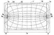
図2Aは、定着フィルム1の概略平面図である。図2Bは、端部領域1d,1fの概略断面図、図2Cは、中央領域1eの概略断面図である。
図2Aに示すように、定着フィルム1において長手方向の中央領域を1eとし、端部領域を1d,1fとする。本実施例では、中央領域1eの長手方向の長さを230mm、端部領域1d,1fの長手方向の長さをそれぞれ10mmとする。
(Characteristics of Example 1)
FIG. 2A is a schematic plan view of the fixing film 1. 2B is a schematic cross-sectional view of the end regions 1d and 1f, and FIG. 2C is a schematic cross-sectional view of the central region 1e.
As shown in FIG. 2A, in the fixing film 1, the central region in the longitudinal direction is 1e, and the end regions are 1d and 1f. In the present embodiment, the longitudinal length of the central region 1e is 230 mm, and the longitudinal lengths of the end regions 1d and 1f are 10 mm, respectively.

定着フィルム1は、膜厚50μmの基層(発熱層)1aと、中央領域1eにおいて基層1aを被覆する膜厚15μmの離型層1bとで構成されている。端部領域1d,1fは、基層1aのみで構成され、離型層1bには被覆されていない。
基層1aには、導電材を添加したポリイミド材を使用する。この基層の抵抗率は230[μΩ・m]、長手方向の抵抗は20Ω(常温25℃の時)である。この基層に電力を投入し、加熱装置の発熱源とする。尚、基層1aは、NTC特性(Negative Temperature Coefficient)を示し、定着フィルム1が200℃に達すると、前述の長手方向の抵抗は約17Ωに変動する。本実施例では、離型層1bにPFAを使用している。
The fixing film 1 includes a base layer (heat generation layer) 1a having a thickness of 50 μm and a release layer 1b having a thickness of 15 μm that covers the base layer 1a in the central region 1e. The end regions 1d and 1f are composed only of the base layer 1a and are not covered with the release layer 1b.
For the base layer 1a, a polyimide material to which a conductive material is added is used. The resistivity of this base layer is 230 [μΩ · m], and the resistance in the longitudinal direction is 20Ω (at room temperature of 25 ° C.). Electric power is applied to this base layer to provide a heat source for the heating device. The base layer 1a exhibits NTC characteristics (Negative Temperature Coefficient), and when the fixing film 1 reaches 200 ° C., the above-mentioned resistance in the longitudinal direction varies to about 17Ω. In this embodiment, PFA is used for the release layer 1b.

図3A〜3Cは、本実施例における加熱装置を示す概略図である。
図3Aには、加熱装置の平面図を示し、図3Bには、給電接点4a,4b、電位接点9a,9bが配置された状態の定着フィルム1の平面図を示し、図3Cには、図3Aに示すB−B断面の断面図を示す。
本実施例の加熱装置101では、定着フィルム1の長手方向の一端に給電接点4a、電位接点9a、電圧計21が接続され、他端に給電接点4b、電位接点9b、電圧計21が接続されている。
図3Bに示すように、定着フィルム1の端部領域1dに給電接点4a、端部領域1fに給電接点4bを接触配置させる。給電接点4a,4bはいずれも同一条件であるため、以下の説明では、給電接点4aについてのみ説明する。
3A to 3C are schematic views showing a heating device in the present embodiment.
3A shows a plan view of the heating device, FIG. 3B shows a plan view of the fixing film 1 in a state where the power supply contacts 4a and 4b and the potential contacts 9a and 9b are arranged, and FIG. Sectional drawing of the BB cross section shown to 3A is shown.
In the heating device 101 of the present embodiment, the feeding contact 4a, the potential contact 9a, and the voltmeter 21 are connected to one end of the fixing film 1 in the longitudinal direction, and the feeding contact 4b, the potential contact 9b, and the voltmeter 21 are connected to the other end. ing.
As shown in FIG. 3B, the feeding contact 4a is placed in contact with the end region 1d of the fixing film 1, and the feeding contact 4b is placed in contact with the end region 1f. Since both of the power supply contacts 4a and 4b have the same conditions, only the power supply contact 4a will be described in the following description.

本実施例において、給電接点4aは銅材であり、給電接点4aの寸法は4mm×4mm×4mmの立方体形状とした。給電接点4aは、定着フィルム1の端縁から長手方向内側に6mm〜10mmの領域内に配置する。
図3Cに示すように、給電接点4aは、定着フィルム1を挟んで定着フランジ5aのツバ部5a2に対向する位置に配置されている。給電接点バネ10は約100gfの押圧力にて、給電接点4を押圧し、給電接点4aと定着フィルム1の接触を安定させる。
給電接点4aと定着フィルム1間の接触抵抗によって電力が無駄に消費されることを極力回避するために、(1)給電接点材の抵抗率を下げる、(2)給電接点の押圧力を上げることが好ましい。
給電接点4aと摺動接触する定着フィルム1の摩耗を軽減したい場合、低い抵抗率の接点材を選択し、給電接点4aの押圧力を下げることが、接触抵抗と定着フィルム1の摩耗の両立の観点で好ましい。
In the present embodiment, the power supply contact 4a is made of a copper material, and the size of the power supply contact 4a is a cube shape of 4 mm × 4 mm × 4 mm. The power supply contact 4 a is disposed in the region of 6 mm to 10 mm in the longitudinal direction from the edge of the fixing film 1.
As shown in FIG. 3C, the power supply contact 4a is disposed at a position facing the flange portion 5a2 of the fixing flange 5a with the fixing film 1 interposed therebetween. The power supply contact spring 10 presses the power supply contact 4 with a pressing force of about 100 gf, and stabilizes the contact between the power supply contact 4 a and the fixing film 1.
In order to avoid the wasteful consumption of power due to the contact resistance between the power supply contact 4a and the fixing film 1, as much as possible (1) lowering the resistivity of the power supply contact material and (2) increasing the pressing force of the power supply contact. Is preferred.
When it is desired to reduce the wear of the fixing film 1 that is in sliding contact with the power supply contact 4a, a contact material having a low resistivity is selected and the pressing force of the power supply contact 4a is lowered, so that both the contact resistance and the wear of the fixing film 1 can be achieved. It is preferable from the viewpoint.

また、図3Bに示すように、定着フィルム1の端部領域1dに電位接点9a、端部領域1fに電位接点9bを接触配置させる。電位接点9aと9bは同一条件であるため、電位接点9aについてのみ説明し、電位接点9bについての説明を省略する。
電位接点9aは、抵抗率10μΩ・m程度のカーボン材とし、寸法は2mm×2mm×2mmの立方体形状とした。電位接点9aは、定着フィルム1の端縁から長手方向内側に6mm〜10mmの領域内に配置する。
図3Cより、定着フィルム1の周面上の周方向における給電接点4aと電位接点9aとの間の距離を“L”とする。実施例1では、L=3mmと設定する。
Further, as shown in FIG. 3B, a potential contact 9a is disposed in contact with the end region 1d of the fixing film 1 and a potential contact 9b is disposed in contact with the end region 1f. Since the potential contacts 9a and 9b have the same conditions, only the potential contact 9a will be described, and description of the potential contact 9b will be omitted.
The potential contact 9a is made of a carbon material having a resistivity of about 10 μΩ · m, and has a cubic shape of 2 mm × 2 mm × 2 mm. The potential contact 9 a is arranged in a region of 6 mm to 10 mm inward in the longitudinal direction from the edge of the fixing film 1.
3C, the distance between the power supply contact 4a and the potential contact 9a in the circumferential direction on the peripheral surface of the fixing film 1 is “L”. In Example 1, L = 3 mm is set.

また、電位接点9aは、定着フィルム1を挟んで定着フランジ5aのツバ部5a2に対向する位置に配置されている。電位接点バネ11aは約10gfの押圧力にて、電位接点9aを押圧するように配置されている。これにより、電位接点9aと定着フィルム1の接触状態を安定させることができる。
電位接点9aは給電接点4aとは異なり、ほぼ電流が流れないため、電位接点9aと定着フィルム1間の接触抵抗が増大したとしても、電力が消費されるわけではない。よって、接触抵抗低減を狙うよりも、電位接点9aによる定着フィルム1の摩耗抑制を優先して電位接点条件を決定することが好ましい。このため本実施例1においては、定着フィルム1よりも低硬度のカーボン材を電位接点9aの材料として使用している。例えば、定着フィルム1の回転に従って回転動作する円柱状の回転体を電位接点9aとして選択してもよい。
図3Aに示すように、給電接点4aと電位接点9aとの間に電圧計21を配置することで、両接点間の電位差を測定することが可能となる。
The potential contact 9a is disposed at a position facing the flange portion 5a2 of the fixing flange 5a with the fixing film 1 interposed therebetween. The potential contact spring 11a is arranged to press the potential contact 9a with a pressing force of about 10 gf. Thereby, the contact state of the potential contact 9a and the fixing film 1 can be stabilized.
Unlike the power supply contact 4a, the electric potential contact 9a hardly flows current. Therefore, even if the contact resistance between the electric potential contact 9a and the fixing film 1 increases, power is not consumed. Therefore, it is preferable to determine the potential contact condition by giving priority to the suppression of wear of the fixing film 1 by the potential contact 9a rather than aiming to reduce the contact resistance. For this reason, in Example 1, a carbon material having a hardness lower than that of the fixing film 1 is used as a material for the potential contact 9a. For example, a cylindrical rotating body that rotates according to the rotation of the fixing film 1 may be selected as the potential contact 9a.
As shown in FIG. 3A, by arranging the voltmeter 21 between the power supply contact 4a and the potential contact 9a, it is possible to measure the potential difference between the two contacts.

(作用)
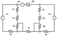
図4は、本実施例における定着フィルム1の等価回路図である。
給電接点4a,4bの抵抗をそれぞれR1,R2、電位接点9a,9bの抵抗をそれぞれR3,R4、給電接点4aと定着フィルム1間の接触抵抗をRc1、給電接点4bと定着フィルム1間の接触抵抗をRc2とする。また、給電接点4aと電位接点9a間の経路抵抗をRf1、給電接点4bと電位接点9b間の経路抵抗をRf2、給電接点4aと給電接点4b間の抵抗をRfとした。
(Function)
FIG. 4 is an equivalent circuit diagram of the fixing film 1 in this embodiment.
The resistances of the power supply contacts 4a and 4b are R1 and R2, the resistances of the potential contacts 9a and 9b are R3 and R4, the contact resistance between the power supply contact 4a and the fixing film 1, Rc1, and the contact between the power supply contact 4b and the fixing film 1, respectively. The resistance is Rc2. The path resistance between the power supply contact 4a and the potential contact 9a is Rf1, the path resistance between the power supply contact 4b and the potential contact 9b is Rf2, and the resistance between the power supply contact 4a and the power contact 4b is Rf.

給電接点4a,4bの抵抗R1,R2はいずれも0.003mΩである。一方、接触抵抗Rc1,Rc2は数百mΩを想定している。抵抗R1,R2は、接触抵抗Rc1,Rc2に比べて十分に小さい。
また、電圧計21の内部抵抗は10MΩであり、図4に示したその他の抵抗に比べ十分に大きい。電位接点9a,9bの抵抗R3,R4には交流電源20の電流は流れないため、抵抗R3,R4に電位差は生じない。
電圧測定において、抵抗R1,R2,R3,R4の電位差は測定されないため、等価回路上における抵抗R1,R2,R3,R4を除外して考えることができる。
The resistances R1, R2 of the power supply contacts 4a, 4b are both 0.003 mΩ. On the other hand, the contact resistances Rc1 and Rc2 are assumed to be several hundred mΩ. The resistors R1 and R2 are sufficiently smaller than the contact resistors Rc1 and Rc2.
The internal resistance of the voltmeter 21 is 10 MΩ, which is sufficiently larger than the other resistances shown in FIG. Since the current of the AC power supply 20 does not flow through the resistors R3 and R4 of the potential contacts 9a and 9b, no potential difference occurs between the resistors R3 and R4.
In the voltage measurement, since the potential difference between the resistors R1, R2, R3, and R4 is not measured, the resistors R1, R2, R3, and R4 on the equivalent circuit can be excluded.

次に、経路抵抗Rf1,Rf2について、図5を用いて説明する。
図5は、定着フィルム1の外周面を示す展開図である。図5において、給電接点4aと給電接点4b間に交流100Vを印加し、約5Aの電流を流した際の電流(電気力線)を実線23で示し、等電位線を点線24で示す。
給電接点4aと電位接点9a間は電気力線が疎であり、両接点間の電位差も小さい。つまり、経路抵抗Rf1の電位差が小さいことが確認できる。それゆえ、電圧測定におけるRf1を測定誤差と考えることができる。経路抵抗Rf2についても同様に考えることができる。
電圧測定おいて抵抗R1,R2,R3,R4を等価回路から除外し、さらに経路抵抗Rf1,Rf2を測定誤差として考えることができるため、図6に示す等価回路に置換えることができる。
Next, the path resistances Rf1 and Rf2 will be described with reference to FIG.
FIG. 5 is a development view showing the outer peripheral surface of the fixing film 1. In FIG. 5, a current (electric field line) when an alternating current of 100 V is applied between the power supply contact 4 a and the power supply contact 4 b and a current of about 5 A flows is indicated by a solid line 23, and an equipotential line is indicated by a dotted line 24.
The lines of electric force are sparse between the power supply contact 4a and the potential contact 9a, and the potential difference between the two contacts is also small. That is, it can be confirmed that the potential difference of the path resistance Rf1 is small. Therefore, Rf1 in voltage measurement can be considered as a measurement error. The same applies to the path resistance Rf2.
In voltage measurement, the resistors R1, R2, R3, and R4 can be excluded from the equivalent circuit, and the path resistors Rf1 and Rf2 can be considered as measurement errors, so that the equivalent circuit shown in FIG. 6 can be substituted.

この等価回路によれば、この電圧測定において接触抵抗Rc1,Rc2の電位差を等価的に測定することが可能になる。
交流電源20に直列に配置する電流計22の指示値(測定値)Iと、給電接点4aと電位接点9a間の電圧計21の指示値Vより、接触抵抗Rc1をV/Iとして算出する。接触抵抗Rc2についても同様にして算出する。
According to this equivalent circuit, the potential difference between the contact resistances Rc1 and Rc2 can be measured equivalently in this voltage measurement.
The contact resistance Rc1 is calculated as V / I from the indicated value (measured value) I of the ammeter 22 arranged in series with the AC power supply 20 and the indicated value V of the voltmeter 21 between the power supply contact 4a and the potential contact 9a. The contact resistance Rc2 is similarly calculated.

以上説明したように、定着フィルム1の基層1aの一端側に電力を供給するための給電接点4aを配置し、同一端側に電位接点9aを配置することで、給電接点4aの接触抵抗をより精度よく測定することができる。
このとき、給電接点4aと電位接点9aとの間に電圧計21を接続し、両接点間の電位差を測定することで、給電接点4aと定着フィルム1との接触抵抗を独立且つ高精度に算出することができる。
As described above, the contact point 4a for supplying power to one end side of the base layer 1a of the fixing film 1 is arranged, and the potential contact 9a is arranged on the same end side, so that the contact resistance of the feed contact point 4a is further increased. It can be measured with high accuracy.
At this time, a voltmeter 21 is connected between the power contact 4a and the potential contact 9a, and the contact resistance between the power contact 4a and the fixing film 1 is calculated independently and with high accuracy by measuring the potential difference between the two contacts. can do.

このように高精度に算出した給電接点4aの接触抵抗は、加熱装置101または画像形成装置100における様々な制御に用いることができる。
ここで、給電接点4aの接触抵抗が大きくなると、給電接点4aと定着フィルム1の間で発熱が生じ、長手方向における最大通紙可能幅より狭いサイズの複数枚の記録材Pを連続で画像形成する場合には、所謂非通紙部昇温が発生することが懸念される。非通紙部昇温は、定着ニップ部Nの長手方向において記録材Pが通過しない領域(非通紙部)の各部材の温度が徐々に上昇するという現象である。加熱装置101としては、非通紙部の温度が装置内の各部材の耐熱温度を超えないようにする必要がある。
そこで、算出された給電接点4aの接触抵抗の値が閾値以上となった場合には、連続プリントのスループット(単位時間(1分)当たりにプリントできる枚数)を低下させる制御(スループットダウン)が行われるものであるとよい。また、算出された給電接点4aの接触抵抗の値が閾値以上となった場合には、画像形成動作を一旦停止させる制御が行われるものであってもよい。また、算出された給電接点4aの接触抵抗の値が閾値以上となった場合には、加熱装置101における制御温度を、設定温度範囲のなかで小さくする制御が行われるものであってもよい。また、算出された給電接点4aの接触抵抗の値が閾値以上となった場合には、交流電源20から供給される電力量を抑える制御が行われるものであってもよい。このような制御により、非通紙部昇温を抑制することができる。
The contact resistance of the power supply contact 4a calculated with high accuracy in this way can be used for various controls in the heating apparatus 101 or the image forming apparatus 100.
Here, when the contact resistance of the power supply contact 4a increases, heat is generated between the power supply contact 4a and the fixing film 1, and a plurality of recording materials P having a size smaller than the maximum sheet passing width in the longitudinal direction are continuously formed. In this case, there is a concern that a so-called non-sheet passing portion temperature rise may occur. The temperature rise of the non-sheet passing portion is a phenomenon in which the temperature of each member gradually increases in a region where the recording material P does not pass in the longitudinal direction of the fixing nip portion N (non-sheet passing portion). As the heating apparatus 101, it is necessary that the temperature of the non-sheet passing portion does not exceed the heat resistance temperature of each member in the apparatus.
Therefore, when the calculated contact resistance value of the power supply contact 4a is equal to or greater than the threshold value, control (throughput reduction) is performed to reduce the throughput of continuous printing (number of sheets that can be printed per unit time (1 minute)). It is good that it is. In addition, when the calculated contact resistance value of the power supply contact 4a is equal to or greater than a threshold value, control for temporarily stopping the image forming operation may be performed. In addition, when the calculated value of the contact resistance of the power supply contact 4a is equal to or greater than a threshold value, control may be performed to reduce the control temperature in the heating device 101 within the set temperature range. In addition, when the calculated contact resistance value of the power supply contact 4a is equal to or greater than a threshold value, control for suppressing the amount of power supplied from the AC power supply 20 may be performed. Such control can suppress the temperature rise of the non-sheet passing portion.

また、本実施例では、一端側に給電接点4aと電位接点9aを配置し、他端側に給電接点4bと電位接点9bを配置するものであったが、これに限るものではない。一端側に配置された給電接点4aと電位接点9aを用いて、他端側の給電接点4bの接触抵抗を予測できるものであれば、他端側には、給電接点4bの接触抵抗を求めるための電位接点9b
が配置されなくてもよい。例えば定着フィルム1の層構成が、一端側と他端側で同じであれば、他端側の給電接点4bの接触抵抗は、一端側の給電接点4aの接触抵抗と同じにすることもできる。また、定着フィルム1の層構成が、一端側と他端側で異なる場合でも、一端側の給電接点4aの接触抵抗と、他端側の給電接点4bの接触抵抗との関係を予め把握しておけば、一端側の給電接点4aの接触抵抗から、他端側の給電接点4bの接触抵抗を予測できる。このような場合には、予め実験等により、一端側の給電接点4aの接触抵抗と、他端側の給電接点4bの接触抵抗との関係を求め、その関係を制御部106に記憶しておくとよい。
In the present embodiment, the power supply contact 4a and the potential contact 9a are arranged on one end side, and the power supply contact 4b and the potential contact 9b are arranged on the other end side, but this is not restrictive. If the contact resistance of the power supply contact 4b on the other end side can be predicted using the power supply contact 4a and the potential contact 9a arranged on one end side, the contact resistance of the power supply contact 4b is obtained on the other end side. Potential contact 9b
May not be arranged. For example, if the layer configuration of the fixing film 1 is the same on the one end side and the other end side, the contact resistance of the power supply contact 4b on the other end side can be the same as the contact resistance of the power supply contact 4a on the one end side. Further, even when the layer configuration of the fixing film 1 is different between the one end side and the other end side, the relationship between the contact resistance of the power supply contact 4a on one end side and the contact resistance of the power supply contact 4b on the other end side is grasped in advance. In this case, the contact resistance of the power supply contact 4b on the other end side can be predicted from the contact resistance of the power supply contact 4a on one end side. In such a case, the relationship between the contact resistance of the power supply contact 4a on one end side and the contact resistance of the power supply contact 4b on the other end side is obtained in advance through experiments or the like, and the relationship is stored in the control unit 106. Good.

また、本実施例においては、給電接点4aと電位接点9aは、定着フィルム1の外周面に接触するように配置しているが、これに限るものではない。すなわち、給電接点4aと電位接点9aを定着フィルム1の内周面に接触するように配置してもよく、このような構成においても、上述した効果と同様の効果を得ることができる。また、一端側において給電接点4aと電位接点9aが、定着フィルム1の外周面に接触するように配置し、他端側において給電接点4bと電位接点9bが、定着フィルム1の内周面に接触するように配置してもよい。
さらに、本実施例における定着フィルム1は基層1aと離型層1bの2層構成であったが、これに限るものではない。例えば、絶縁層、発熱層、離型層の順に配置される多層定着フィルムであっても、上述したように給電接点4aと電位接点9aを発熱層に接触して配置すれば、上述した効果と同様の効果を得ることができる。
In this embodiment, the power contact 4a and the potential contact 9a are arranged so as to contact the outer peripheral surface of the fixing film 1, but the present invention is not limited to this. That is, the power supply contact 4a and the potential contact 9a may be arranged so as to be in contact with the inner peripheral surface of the fixing film 1. Even in such a configuration, the same effect as described above can be obtained. Further, the power supply contact 4 a and the potential contact 9 a are arranged so as to contact the outer peripheral surface of the fixing film 1 on one end side, and the power supply contact 4 b and the potential contact 9 b contact the inner peripheral surface of the fixing film 1 on the other end side. You may arrange so that.
Furthermore, although the fixing film 1 in this embodiment has a two-layer configuration of the base layer 1a and the release layer 1b, it is not limited to this. For example, even in the case of a multilayer fixing film arranged in the order of an insulating layer, a heat generation layer, and a release layer, if the power supply contact 4a and the potential contact 9a are arranged in contact with the heat generation layer as described above, the above-described effects can be obtained. Similar effects can be obtained.

以下に、給電接点4aに対する電位接点9aの好適な位置について検討した結果について説明する。
図7は、定着フィルム1の外周面を示す展開図である。図7において、交流電源20により給電接点4aと給電接点4bとの間に電圧を印加した際の、電流(電気力線)を実線23で示し、等電位線を点線24で示す。
ここでは、電位接点9aを異なる4箇所に配置した場合について比較した。
9a1・・・給電接点4aより長手方向内側
9a2・・・長手方向において給電接点4aと同位置
9a3・・・長手方向において給電接点4aと同位置(9a2と周方向で異なる位置)
9a4・・・給電接点4aより長手方向外側(定着フィルム1の端縁側)
いずれの電位接点も給電接点4aとの距離Lを3mmとした。
Below, the result of having examined the suitable position of the electric potential contact 9a with respect to the electric power feeding contact 4a is demonstrated.
FIG. 7 is a development view showing the outer peripheral surface of the fixing film 1. In FIG. 7, when a voltage is applied between the power supply contact 4 a and the power supply contact 4 b by the AC power supply 20, a current (electric force line) is indicated by a solid line 23, and an equipotential line is indicated by a dotted line 24.
Here, a comparison was made for the case where the potential contacts 9a are arranged at four different locations.
9a1... Inward in the longitudinal direction from the power supply contact 4a. 9a2... Same position as the power supply contact 4a in the longitudinal direction 9a3... Same position as the power supply contact 4a in the longitudinal direction (a position different from 9a2 in the circumferential direction)
9a4: Longitudinal outside of the power supply contact 4a (edge side of the fixing film 1)
In any potential contact, the distance L from the power supply contact 4a was 3 mm.

図6の等価回路によれば、給電接点4aから定着フィルム1を経て電位接点9aに至るまでの経路の抵抗Rf1における電位差の大小は、電圧測定における経路抵抗Rf1の測定誤差を左右する。経路抵抗Rf1の電位差を小さくすればするほど、測定誤差の低減につながり、接触抵抗算出の精度向上にとって好ましい。
図7より、給電接点4aに電位接点9aを近づけるほど、電位差は小さくなる。よって、両接点間の距離を近接することが好ましいことがわかる。
According to the equivalent circuit of FIG. 6, the magnitude of the potential difference in the resistance Rf1 of the path from the power supply contact 4a through the fixing film 1 to the potential contact 9a affects the measurement error of the path resistance Rf1 in voltage measurement. The smaller the potential difference of the path resistance Rf1, the lower the measurement error, which is preferable for improving the accuracy of contact resistance calculation.
From FIG. 7, the closer the potential contact 9a is to the power supply contact 4a, the smaller the potential difference becomes. Therefore, it can be seen that it is preferable to make the distance between the two contacts close.

(電位接点9a1の位置)
電位接点9a1の位置は他の3つの位置と比較して、やや電位差が大きい。給電接点4aより長手方向内側に電位接点を配置する際は、極力両接点の距離を近接することが望まれる。一方で、給電接点4aより長手方向外側に配置する必要がないので、例えば定着フィルム1の長手方向の長さを伸ばす等の装置サイズ拡大の心配がない。
(電位接点9a2と電位接点9a3の位置)
長手方向において同位置且つ接点間距離が同一である電位接点9a2と電位接点9a3においては、電位差は同等であり、どちらの電位接点であっても同様の効果を発揮する。前述した電位接点9a1の位置より電位差が生じにくい接点配置である。また、電位接点9a1の時と同様に給電接点4aより長手方向外側に配置する必要がないので、例えば定
着フィルム1の長手方向の長さを伸ばす等の装置サイズ拡大の心配がない。
(電位接点9a4の位置)
電位接点9a4の位置は他の3つの電位接点の位置と比較して、最も電位差が生じにくいので、測定精度を優先する場合は定着フィルム1の長手方向において、給電接点4aの外側配置が好ましい。
(Position of potential contact 9a1)
The position of the potential contact 9a1 is slightly larger than the other three positions. When arranging the potential contact on the inner side in the longitudinal direction from the power supply contact 4a, it is desirable to make the distance between the two contacts as close as possible. On the other hand, since there is no need to dispose the power supply contact 4a on the outside in the longitudinal direction, there is no fear of expanding the apparatus size, for example, extending the length of the fixing film 1 in the longitudinal direction.
(Position of potential contact 9a2 and potential contact 9a3)
The potential contact 9a2 and the potential contact 9a3, which have the same position in the longitudinal direction and the same distance between the contacts, have the same potential difference, and the same effect is exhibited regardless of the potential contact. The contact arrangement is such that a potential difference is less likely to occur than the position of the potential contact 9a1 described above. Further, as in the case of the potential contact 9a1, it is not necessary to dispose the power contact 4a on the outer side in the longitudinal direction, so that there is no concern about the enlargement of the apparatus size such as extending the length of the fixing film 1 in the longitudinal direction.
(Position of potential contact 9a4)
Since the position of the potential contact 9a4 is most unlikely to cause a potential difference as compared with the positions of the other three potential contacts, the outer side of the power supply contact 4a is preferably arranged in the longitudinal direction of the fixing film 1 when priority is given to measurement accuracy.

以上のように、給電接点4aと電位接点9aとを近づけることで、両接点間の電位差を低減できる。したがって、両接点を極力近接させることが好ましい。
そして、両接点を可能な限り近接配置した上で、測定精度を優先する場合、給電接点4aより長手方向外側に電位接点9aを配置することが好ましい。
As described above, the potential difference between the two contacts can be reduced by bringing the power supply contact 4a and the potential contact 9a closer to each other. Therefore, it is preferable to make both contacts as close as possible.
And when placing both contacts as close as possible and giving priority to measurement accuracy, it is preferable to arrange the potential contact 9a on the outer side in the longitudinal direction from the power supply contact 4a.

ここで、定着フィルム1の内周側で粘性の高い摺動グリスなどを使用する際には、本実施例のように、2つの接点を定着フィルム1の外周側に配置することが望ましい。給電接点4aにグリスが付着することで接触抵抗の上昇を招くおそれがあるからでる。また、電位接点9aにグリスが付着することで、定着フィルム1との導通経路が途切れ、電位の測定を不可能にするおそれがある。
一方、定着フィルム1の外周面がトナーや粉塵などで汚染されやすい構成を選択する場合、2つの接点は、定着フィルム1の内周側に配置するのが望ましい。前述と同様に、2つの接点にトナーや粉塵が付着することで、接触抵抗の上昇や測定不能になるおそれがあるからである。
加熱装置101の仕様及び外乱に対応するよう、状況に応じて定着フィルム1の外周側に配置するか内周側に配置するかを選択するとよい。
Here, when using a highly viscous sliding grease or the like on the inner peripheral side of the fixing film 1, it is desirable to dispose two contacts on the outer peripheral side of the fixing film 1 as in this embodiment. This is because grease may adhere to the power supply contact 4a and increase the contact resistance. Further, when grease adheres to the potential contact 9a, the conduction path to the fixing film 1 is interrupted, which may make it impossible to measure the potential.
On the other hand, when selecting a configuration in which the outer peripheral surface of the fixing film 1 is easily contaminated with toner or dust, the two contact points are preferably arranged on the inner peripheral side of the fixing film 1. This is because, as described above, toner or dust adheres to the two contact points, which may increase the contact resistance or make measurement impossible.
In order to correspond to the specification and disturbance of the heating device 101, it is preferable to select whether to arrange on the outer peripheral side or the inner peripheral side of the fixing film 1 depending on the situation.

(実施例2)
以下に、実施例2について説明する。なお、本実施例においては、実施例1に対して異なる構成部分について述べることとし、実施例1と同様の構成部分については、その説明を省略する。
本実施例の特徴は、定着フィルム1の両端部に低抵抗層(低抵抗導電層)を配置し、その低抵抗層に給電接点及び電位接点を接触配置していることである。
図8Aは、本実施例の定着フィルム1の概略平面図である。図8Bは、端部領域1d,1fの概略断面図、図8Cは、中央領域1eの概略断面図である。
(Example 2)
Example 2 will be described below. In the present embodiment, the different components from the first embodiment will be described, and the description of the same components as those in the first embodiment will be omitted.
The feature of this embodiment is that a low resistance layer (low resistance conductive layer) is disposed at both ends of the fixing film 1, and a power supply contact and a potential contact are disposed in contact with the low resistance layer.
FIG. 8A is a schematic plan view of the fixing film 1 of the present embodiment. 8B is a schematic cross-sectional view of the end regions 1d and 1f, and FIG. 8C is a schematic cross-sectional view of the central region 1e.

本実施例の定着フィルム1は、実施例1同様、膜厚50μmの基層1aと、中央領域1eにおいて基層1aを被覆する膜厚15μmの離型層1bとを有し、さらに、端部領域1d,1fにおいて基層1aを被覆する膜厚10μmの低抵抗層1cを有する。ここで、基層1aと低抵抗層1cは電気的に接続している。基層1a、離型層1bについては実施例1と同様である。低抵抗層1cには、抵抗率0.1μΩ・mの銀ペースト材を使用する。この低抵抗層1cは、基層1aに比べて十分に抵抗率が低いため、低抵抗層1cを被覆した端部領域1d,1fの基層1aでは発熱しない。   As in Example 1, the fixing film 1 of this example has a base layer 1a having a thickness of 50 μm, a release layer 1b having a thickness of 15 μm covering the base layer 1a in the central region 1e, and an end region 1d. , 1f includes a low resistance layer 1c having a thickness of 10 μm covering the base layer 1a. Here, the base layer 1a and the low resistance layer 1c are electrically connected. The base layer 1a and the release layer 1b are the same as in Example 1. A silver paste material having a resistivity of 0.1 μΩ · m is used for the low resistance layer 1c. Since the low resistance layer 1c has a sufficiently low resistivity as compared with the base layer 1a, the base layer 1a in the end regions 1d and 1f covering the low resistance layer 1c does not generate heat.

図9A〜9Cは、定着フィルム1の一端に給電接点4a、電位接点9a、電圧計21、別の一端に給電接点4b、電位接点9b、電圧計21を接続した加熱装置の概略図である。
図9Aには、加熱装置の平面図、図9Bには、給電接点4a,4b、電位接点9a,9bが接続された状態の定着フィルム1の平面図を示し、図9Cには、図9AにおけるC−C断面の断面図を示す。
本実施例では、図9Bに示すように、定着フィルム1の端部領域1dに給電接点4a、端部領域1fに給電接点4bを接触配置させる。給電接点4a,4bは同一条件であるため、本実施例においても、給電接点4aについてのみ説明する。
本実施例では、定着フィルム1の端部領域1dにおいて、基層1aの外周面上に低抵抗
層1cを設けており、この低抵抗層1cと給電接点4aを接触させることで交流電源20から定着フィルム1に電力を供給することを特徴とする。
9A to 9C are schematic views of a heating apparatus in which the feeding contact 4a, the potential contact 9a, and the voltmeter 21 are connected to one end of the fixing film 1, and the feeding contact 4b, the potential contact 9b, and the voltmeter 21 are connected to the other end.
9A shows a plan view of the heating device, FIG. 9B shows a plan view of the fixing film 1 in a state where the power supply contacts 4a and 4b and the potential contacts 9a and 9b are connected, and FIG. 9C shows the plan view of FIG. 9A. Sectional drawing of CC cross section is shown.
In this embodiment, as shown in FIG. 9B, the feeding contact 4a is disposed in contact with the end region 1d of the fixing film 1, and the feeding contact 4b is disposed in contact with the end region 1f. Since the power supply contacts 4a and 4b have the same conditions, only the power supply contact 4a will be described in this embodiment.
In this embodiment, a low resistance layer 1c is provided on the outer peripheral surface of the base layer 1a in the end region 1d of the fixing film 1, and the low resistance layer 1c is brought into contact with the power supply contact 4a to fix from the AC power source 20. Electricity is supplied to the film 1.

また、図9Bに示すように、定着フィルム1の端部領域1dに電位接点9a、端部領域1fに電位接点9bを接触配置させる。電位接点9a,9bは同一条件であるため、本実施例においても、電位接点9aについてのみ説明する。
本実施例では、定着フィルム1の端部領域1d,1fにおいて、基層1aの外周面上に設けられた低抵抗層1cに電位接点9aを接触させ、給電接点4aと電位接点9a間の電位差を測定する。
Further, as shown in FIG. 9B, a potential contact 9a is placed in contact with the end region 1d of the fixing film 1 and a potential contact 9b is placed in contact with the end region 1f. Since the potential contacts 9a and 9b have the same conditions, only the potential contact 9a will be described in this embodiment.
In this embodiment, in the end regions 1d and 1f of the fixing film 1, the potential contact 9a is brought into contact with the low resistance layer 1c provided on the outer peripheral surface of the base layer 1a, and the potential difference between the power supply contact 4a and the potential contact 9a is determined. taking measurement.

(作用)
本実施例における定着フィルム1の等価回路は、実施例1と同様となる。よって、図4に示した等価回路を利用して以下に説明する。
実施例1と同じ理由から、電圧測定において、抵抗R1,R2,R3,R4の電位差は測定されないため、等価回路上における抵抗R1,R2,R3,R4を除外して考えることができる。
(Function)
The equivalent circuit of the fixing film 1 in this embodiment is the same as that in the first embodiment. Therefore, the following description will be made using the equivalent circuit shown in FIG.
For the same reason as in the first embodiment, in voltage measurement, the potential difference between the resistors R1, R2, R3, and R4 is not measured. Therefore, the resistors R1, R2, R3, and R4 on the equivalent circuit can be excluded.

次に、給電接点4a,4bから定着フィルム1を経て電位接点9a,9bに至るまでの経路の抵抗Rf1,Rf2について、図10を用いて説明する。
図10は、定着フィルム1の外周面を示す展開図である。図10において、給電接点4aと給電接点4b間に交流100Vを印加し、約5Aの電流を流した際の、電流(電気力線)を実線23で示し、等電位線を点線24で示す。図10に示すように、電流(電気力線)は定着フィルム1の長手方向に略平行に均一に流れ、等電位線は、定着フィルム1の長手方向に対して垂直な方向に均一である。また、給電接点4aと電位接点9a間は同電位であるため、両接点間には電流が流れない。つまり、給電接点4aと電位接点9a間には電位差が生じないので、電圧測定において、等価回路上における経路抵抗Rf1を除外して考えることができる。同様の理由より給電接点4bと電位接点9b間にも電位差が生じないので、経路抵抗Rf2を除外して考えることができる。
Next, the resistances Rf1 and Rf2 of the path from the power supply contacts 4a and 4b to the potential contacts 9a and 9b through the fixing film 1 will be described with reference to FIG.
FIG. 10 is a development view showing the outer peripheral surface of the fixing film 1. In FIG. 10, when an alternating current of 100 V is applied between the power supply contact 4 a and the power supply contact 4 b and a current of about 5 A is applied, the current (electric force line) is indicated by a solid line 23, and the equipotential line is indicated by a dotted line 24. As shown in FIG. 10, the current (electric field lines) flows uniformly in parallel with the longitudinal direction of the fixing film 1, and the equipotential lines are uniform in the direction perpendicular to the longitudinal direction of the fixing film 1. In addition, since the power contact 4a and the potential contact 9a are at the same potential, no current flows between the contacts. That is, since no potential difference is generated between the power supply contact 4a and the potential contact 9a, the voltage resistance can be considered by excluding the path resistance Rf1 on the equivalent circuit. For the same reason, there is no potential difference between the power supply contact 4b and the potential contact 9b, so that the path resistance Rf2 can be excluded.

以上のことから、電圧測定おいて抵抗R1,R2,R3,R4,Rf1,Rf2を等価回路から除外して考えることができる。このため、図4に示す等価回路を図11に示す等価回路に置換えることができる。
本実施例の電圧測定においては、図11に示す等価回路を用いて、接触抵抗Rc1,Rc2の電位差を等価的に測定することが可能になる。
From the above, it is possible to exclude the resistors R1, R2, R3, R4, Rf1, and Rf2 from the equivalent circuit in voltage measurement. Therefore, the equivalent circuit shown in FIG. 4 can be replaced with the equivalent circuit shown in FIG.
In the voltage measurement of this embodiment, the potential difference between the contact resistances Rc1 and Rc2 can be measured equivalently using the equivalent circuit shown in FIG.

以上説明したように、円筒状の定着フィルム1の基層1aの一端側に低抵抗層1cを配置し、その低抵抗層1cに電力を供給する給電接点4a、同一端側且つ低抵抗層1cに電位接点9aを接触配置させることで接触抵抗をより精度よく測定することができる。
また、給電接点4aと電位接点9aとの間に電圧計21を接続し、両接点間の電位差を測定することで、給電接点4aと定着フィルム1との接触抵抗を独立且つ高精度に算出することができる。
As described above, the low resistance layer 1c is disposed on one end side of the base layer 1a of the cylindrical fixing film 1, and the power supply contact 4a for supplying power to the low resistance layer 1c is connected to the same end side and the low resistance layer 1c. By placing the potential contact 9a in contact, the contact resistance can be measured more accurately.
Further, by connecting a voltmeter 21 between the power supply contact 4a and the potential contact 9a and measuring the potential difference between the two contacts, the contact resistance between the power supply contact 4a and the fixing film 1 is calculated independently and with high accuracy. be able to.

ここで、本実施例においては、低抵抗層1cの材質として銀ペースト材を選択しているが、これに限るものではない。例えば金、銀、銅、ニッケルメッキ等で低抵抗層1cを形成してもよいし、金属製のリングを定着フィルム1の端部に接着等してもよく、このような構成によっても上述した効果と同様の効果を得ることができる。
また、本実施例において低抵抗層1cは、基層1aの外周面上に設けられるものであったが、これに限るものではない。低抵抗層1cは、基層1aの内周面上に設けられるものであってもよく、基層1aの外周面上と内周面上にそれぞれ設けられるものであってもよい。このような構成によっても上述した効果と同様の効果を得ることができる。
また、本実施例では、定着フィルム1の端部領域1dにおいて、低抵抗層1cを設け、給電接点4aおよび電位接点9aと、低抵抗層1cとをそれぞれ接触させるものであったが、これに限るものではない。すなわち、給電接点4aおよび電位接点9aのうちいずれか一方が、低抵抗層1cと接触し、他方が基層1aと接触するように配置されるものであってもよい。
Here, in this embodiment, the silver paste material is selected as the material of the low resistance layer 1c, but the present invention is not limited to this. For example, the low resistance layer 1c may be formed by gold, silver, copper, nickel plating or the like, or a metal ring may be bonded to the end of the fixing film 1 or the like. An effect similar to the effect can be obtained.
In the present embodiment, the low resistance layer 1c is provided on the outer peripheral surface of the base layer 1a, but is not limited thereto. The low resistance layer 1c may be provided on the inner peripheral surface of the base layer 1a, or may be provided on each of the outer peripheral surface and the inner peripheral surface of the base layer 1a. Even with such a configuration, the same effect as described above can be obtained.
In this embodiment, the low resistance layer 1c is provided in the end region 1d of the fixing film 1, and the power supply contact 4a, the potential contact 9a, and the low resistance layer 1c are brought into contact with each other. It is not limited. That is, any one of the power supply contact 4a and the potential contact 9a may be arranged so as to be in contact with the low resistance layer 1c and the other in contact with the base layer 1a.

(実施例3)
以下に、実施例3について説明する。なお、本実施例においては、実施例1,2に対して異なる構成部分について述べることとし、実施例1,2と同様の構成部分については、その説明を省略する。
本実施例の特徴は、給電接点と電位接点を、それぞれの接点が定着フィルム1を挟んで対向するように、定着フィルム1の内周面と外周面にそれぞれ接触配置していることである。
(Example 3)
Example 3 will be described below. In the present embodiment, different components from those of the first and second embodiments will be described, and the description of the same components as those of the first and second embodiments will be omitted.
The feature of this embodiment is that the feeding contact and the potential contact are arranged in contact with the inner peripheral surface and the outer peripheral surface of the fixing film 1 so that the respective contacts face each other with the fixing film 1 interposed therebetween.

図12A〜12Cは、定着フィルム1の一端に給電接点4a、電位接点9a、電圧計21、別の一端に給電接点4b、電位接点9b、電圧計21を接続した加熱装置の概略図である。図12Aには、加熱装置の平面図、図12Bには、給電接点4a,4b、電位接点9a,9bが接続された状態の定着フィルム1の平面図を示し、図12Cには、図12AにおけるD−D断面の断面図を示す。
図12Bに示すように、定着フィルム1の外周面において、端部領域1dに給電接点4a、端部領域1fに給電接点4bを接触配置させる。給電接点4a,4bは同一条件であるため、本実施例においても、給電接点4aについてのみ説明する。
本実施例では図12Cに示すように、電位接点9aは、定着フランジ5aのツバ部5a2上に配置され、定着フィルム1の内周面に接触している。そして、給電接点4aは、定着フィルム1を挟んで、電位接点9aに対向配置されている。
12A to 12C are schematic views of a heating apparatus in which the feeding contact 4a, the potential contact 9a, and the voltmeter 21 are connected to one end of the fixing film 1, and the feeding contact 4b, the potential contact 9b, and the voltmeter 21 are connected to the other end. 12A shows a plan view of the heating device, FIG. 12B shows a plan view of the fixing film 1 in a state where the power supply contacts 4a and 4b and the potential contacts 9a and 9b are connected, and FIG. 12C shows the plan view of FIG. 12A. Sectional drawing of DD cross section is shown.
As shown in FIG. 12B, on the outer peripheral surface of the fixing film 1, the power supply contact 4a is disposed in contact with the end region 1d, and the power supply contact 4b is disposed in contact with the end region 1f. Since the power supply contacts 4a and 4b have the same conditions, only the power supply contact 4a will be described in this embodiment.
In this embodiment, as shown in FIG. 12C, the potential contact 9 a is disposed on the flange 5 a 2 of the fixing flange 5 a and is in contact with the inner peripheral surface of the fixing film 1. The power supply contact 4a is disposed opposite to the potential contact 9a with the fixing film 1 interposed therebetween.

図13A〜13Cは、本実施例において、端部領域1dの給電接点部の概略図である。図13Aは、定着フランジ5aと加圧バネ8を示す図、図13Bは、図13Aに電位接点9aを追加して表示した図、図13Cは、図13Bに定着フィルム1、給電接点4a、給電バネ10を追加して表示した図である。なお、図13B,13Cにおいては、説明の便宜上、電位接点9a、給電バネ10、端部領域1d、中央領域1eにハッチングを施している。
定着フィルム1の端部領域1fにおける電位接点9bに関しても、端部領域1dにおける電位接点9aと同様のため、その説明は省略する。
13A to 13C are schematic views of the power supply contact portion in the end region 1d in the present embodiment. 13A shows the fixing flange 5a and the pressure spring 8, FIG. 13B shows the potential contact 9a added to FIG. 13A, and FIG. 13C shows the fixing film 1, the power supply contact 4a, and the power supply in FIG. 13B. It is the figure which added and displayed the spring. 13B and 13C, for convenience of explanation, the potential contact 9a, the feeding spring 10, the end region 1d, and the central region 1e are hatched.
Since the potential contact 9b in the end region 1f of the fixing film 1 is the same as the potential contact 9a in the end region 1d, the description thereof is omitted.

本実施例では図13Bに示すように、電位接点9aとして5mm幅の銅箔テープを定着フランジ5aのツバ部5a2から定着フランジ5aの胴体部5a1まで連続して貼付している。実施例1や実施例2における電位接点の保持方法とは異なり、本実施例では電位接点9aは定着フランジ5aによって位置が決定される。この定着フランジ5aは、加熱装置101の不図示の金属フレームによって位置が固定されており、定着フランジ5aの位置が変動することはほぼない。よって、電位接点9aの位置に関しても変動することはほぼない。
定着フランジ5aのツバ部5a2が、図13Bに示す状態から、定着フィルム1の内周側に挿し込まれることで、図13Cに示すように、定着フランジ5aと定着フィルム1が組立てられている。
給電接点バネ10は、給電接点4a、定着フィルム1を経て電位接点9aに対して押圧力を付与している。定着フランジ5aの胴体部5a1に貼付されている電位接点9aは、電圧計21に接続されている。
In this embodiment, as shown in FIG. 13B, a copper foil tape having a width of 5 mm is continuously applied as the potential contact 9a from the flange portion 5a2 of the fixing flange 5a to the body portion 5a1 of the fixing flange 5a. Unlike the method for holding the potential contact in the first and second embodiments, in this embodiment, the position of the potential contact 9a is determined by the fixing flange 5a. The position of the fixing flange 5a is fixed by a metal frame (not shown) of the heating device 101, and the position of the fixing flange 5a hardly changes. Therefore, the position of the potential contact 9a hardly changes.
The flange portion 5a2 of the fixing flange 5a is inserted into the inner peripheral side of the fixing film 1 from the state shown in FIG. 13B, whereby the fixing flange 5a and the fixing film 1 are assembled as shown in FIG. 13C.
The power supply contact spring 10 applies a pressing force to the potential contact 9 a through the power supply contact 4 a and the fixing film 1. A potential contact 9 a attached to the body 5 a 1 of the fixing flange 5 a is connected to a voltmeter 21.

ここで、本実施例においては上述したように、給電接点4aと電位接点9aは定着フィ
ルム1を挟んで対向配置されている。このような構成においては、給電接点4aと電位接点9aのうちどちらか一方のみに接点バネ(押圧部材)を備え、もう一方は位置を固定する方が望ましい。例えば、どちらの接点にも接点バネを備えた場合、接点バネの押圧力変化、バネの伸縮、定着フィルム1の回転軌跡変動などによって、定着フィルムはどちらかの接点に近づいたり遠ざかったりするなど、定着フィルム1の位置が定まらなくなることが懸念される。定着フィルム1の位置が定まらない場合には、定着フィルム1が他の構成部品に接触するなどして、定着フィルム1がダメージを受けるリスクがある。
本実施例では、位置が固定された電位接点9aに定着フィルム1が押しつけられる構成であるため、定着フィルム1の位置が変動することはほぼない。よって、本実施例の構成により、前述のリスクを最小限に留めることができる。
Here, in the present embodiment, as described above, the power supply contact 4a and the potential contact 9a are opposed to each other with the fixing film 1 interposed therebetween. In such a configuration, it is preferable that only one of the power supply contact 4a and the potential contact 9a is provided with a contact spring (pressing member) and the other is fixed in position. For example, when both contact points are provided with contact springs, the fixing film moves closer to or away from either contact point due to changes in the pressing force of the contact springs, expansion and contraction of the springs, fluctuations in the rotation trajectory of the fixing film 1, etc. There is a concern that the position of the fixing film 1 may not be determined. If the position of the fixing film 1 is not fixed, there is a risk that the fixing film 1 may be damaged due to the fixing film 1 coming into contact with other components.
In this embodiment, since the fixing film 1 is pressed against the potential contact 9a whose position is fixed, the position of the fixing film 1 hardly varies. Therefore, the above-described risk can be minimized by the configuration of the present embodiment.

(作用)
図14は、本実施例における定着フィルムの等価回路図である。
抵抗R1,R2,R3,R4,Rc1,Rc2,Rf1,Rf2,Rfについては実施例1と同様の定義とする。
実施例1と同様の理由から、抵抗R1,R2は接触抵抗Rc1,Rc2に比べて十分に小さい。また、電位接点材の抵抗R3,R4には交流電源20の電流は流れないため、抵抗R3,R4に電位差は生じない。
電圧測定において、抵抗R1,R2,R3,R4の電位差は測定されないため、等価回路上における抵抗R1,R2,R3,R4を除外して考えることができる。
(Function)
FIG. 14 is an equivalent circuit diagram of the fixing film in this example.
The resistors R1, R2, R3, R4, Rc1, Rc2, Rf1, Rf2, and Rf have the same definitions as in the first embodiment.
For the same reason as in the first embodiment, the resistors R1 and R2 are sufficiently smaller than the contact resistors Rc1 and Rc2. In addition, since the current from the AC power supply 20 does not flow through the resistors R3 and R4 of the potential contact material, no potential difference occurs between the resistors R3 and R4.
In the voltage measurement, since the potential difference between the resistors R1, R2, R3, and R4 is not measured, the resistors R1, R2, R3, and R4 on the equivalent circuit can be excluded.

次に、経路抵抗Rf1について考える。
給電接点4aと電位接点9aとの間には、膜厚50μmの定着フィルム1の基層1aのみが介在する。基層1aの抵抗率と膜厚、両接点の寸法より、両接点間の経路抵抗Rf1はそれぞれ約0.5mΩと算出できる。よって、この経路抵抗Rf1についてもRc1に比べて十分に小さいため、図14に示す等価回路図から除外できる。経路抵抗Rf2についても同様である。
したがって、電圧測定おいて抵抗R1,R2,R3,R4,Rf,Rf2を等価回路から除外して考えることができるため、この電圧測定において接触抵抗Rc1,Rc2の電位差を等価的に測定することが可能になる。
Next, the path resistance Rf1 will be considered.
Only the base layer 1a of the fixing film 1 having a film thickness of 50 μm is interposed between the power supply contact 4a and the potential contact 9a. From the resistivity and film thickness of the base layer 1a and the dimensions of both contacts, the path resistance Rf1 between the two contacts can be calculated to be about 0.5 mΩ. Therefore, this path resistance Rf1 is also sufficiently smaller than Rc1, and can be excluded from the equivalent circuit diagram shown in FIG. The same applies to the path resistance Rf2.
Therefore, since the resistors R1, R2, R3, R4, Rf, and Rf2 can be excluded from the equivalent circuit in the voltage measurement, the potential difference between the contact resistors Rc1 and Rc2 can be measured equivalently in this voltage measurement. It becomes possible.

以上説明したように、定着フィルム1の基層1aの外周面に給電接点4a、内周面に電位接点9aを接触配置し、両接点を対向配置させることで、接触抵抗をより精度よく測定することができる。
また、給電接点4aと電位接点9aとの間に電圧計21を接続し、両接点間の電位差を測定することで、給電接点4aと定着フィルム1との接触抵抗を独立且つ高精度に算出することができる。
As described above, the contact resistance is measured more accurately by arranging the power contact 4a on the outer peripheral surface of the base layer 1a of the fixing film 1 and the potential contact 9a on the inner peripheral surface, and arranging both the contacts to face each other. Can do.
Further, by connecting a voltmeter 21 between the power supply contact 4a and the potential contact 9a and measuring the potential difference between the two contacts, the contact resistance between the power supply contact 4a and the fixing film 1 is calculated independently and with high accuracy. be able to.

ここで、実施例1では、給電接点4aと電位接点9aとの間の距離Lを3mmと設定したが、この距離Lを0.5mmにするなど縮めすぎた場合には、給電接点4aと電位接点9aが接触してしまうことが懸念される。給電接点4aと電位接点9aが接触した場合には、給電接点4aから電位接点9aを経てさらに、定着フィルム1へと流れる電流経路が発生する可能性がある。この電流経路の発生は、電圧測定によって不要な電位差を発生させるため、電圧測定の精度を低下させるおそれがある。ゆえに、給電接点4aと電位接点9aは直接接触しないように所定の距離を離して配置することが望ましい。
一方で、本実施例では、給電接点4aと電位接点9aを定着フィルム1を挟んで配置しているため、給電接点4aと電位接点9aは同一面上には位置していない。この場合、給電接点4aと電位接点9aの距離は定着フィルム1の膜厚に等しくなる。本実施例では、定着フィルム1の膜厚を50μmとしているので、両接点間の距離を50μmと非常に短く設定できることが利点となる。すなわち、給電接点4aと電位接点9aとの間に定着フ
ィルム1が介在するので、両接点間の距離を縮小したうえで、両接点が直接接触しない構成を実現することができる。
Here, in Example 1, the distance L between the power contact 4a and the potential contact 9a is set to 3 mm. However, when the distance L is reduced too much, for example, 0.5 mm, the power contact 4a and the potential There is concern about the contact 9a coming into contact. When the power supply contact 4a and the potential contact 9a come into contact with each other, there is a possibility that a current path flowing from the power supply contact 4a to the fixing film 1 through the potential contact 9a may be generated. The generation of this current path generates an unnecessary potential difference by voltage measurement, which may reduce the accuracy of voltage measurement. Therefore, it is desirable to arrange the power supply contact 4a and the potential contact 9a at a predetermined distance so as not to directly contact each other.
On the other hand, in this embodiment, since the power supply contact 4a and the potential contact 9a are arranged with the fixing film 1 interposed therebetween, the power supply contact 4a and the potential contact 9a are not located on the same plane. In this case, the distance between the power supply contact 4 a and the potential contact 9 a is equal to the film thickness of the fixing film 1. In this embodiment, since the film thickness of the fixing film 1 is 50 μm, it is advantageous that the distance between both contacts can be set to a very short value of 50 μm. That is, since the fixing film 1 is interposed between the power supply contact 4a and the potential contact 9a, it is possible to realize a configuration in which both the contacts are not in direct contact with each other while reducing the distance between the both contacts.

また、本実施例では、給電接点4aを定着フィルム1の外周側、電位接点9aを定着フィルム1の内周側に配置したが、これに限るものではない。給電接点4aを定着フィルム1の内周側、電位接点9aを定着フィルム1の外周側に配置したとしても、本実施例と同等の効果を得ることができる。
また、定着フィルム1の長手方向の端部において、基層1aの外周面若しくは内周面に、実施例2のように低抵抗層を設けてもよく、この場合、実施例2で示した理由より、本実施例と同等以上の効果を得ることができる。
以上説明した各実施例は、本発明の実施形態の例示を旨とするものであり、本発明の要旨を逸脱しない範囲内において、可能な限り組み合わせたり、種々の変更を加えたりすることが可能である。
In this embodiment, the power contact 4a is disposed on the outer peripheral side of the fixing film 1 and the potential contact 9a is disposed on the inner peripheral side of the fixing film 1. However, the present invention is not limited to this. Even if the power supply contact 4a is arranged on the inner peripheral side of the fixing film 1 and the potential contact 9a is arranged on the outer peripheral side of the fixing film 1, the same effect as in this embodiment can be obtained.
Further, a low resistance layer may be provided on the outer peripheral surface or the inner peripheral surface of the base layer 1a at the end in the longitudinal direction of the fixing film 1 as in Example 2, and in this case, for the reason shown in Example 2 An effect equivalent to or greater than that of the present embodiment can be obtained.
Each example described above is intended to exemplify the embodiment of the present invention, and can be combined or variously modified as much as possible without departing from the gist of the present invention. It is.

1…定着フィルム、1a…基層、3…加圧ローラ、4a,4b…給電接点、9a,9b…電位接点、101…加熱装置、P…記録材
DESCRIPTION OF SYMBOLS 1 ... Fixing film, 1a ... Base layer, 3 ... Pressure roller, 4a, 4b ... Feed contact, 9a, 9b ... Potential contact, 101 ... Heating device, P ... Recording material

Claims (9)

電力が供給されることで発熱する発熱層を有する可撓性スリーブを有し、
画像が形成された記録材を、前記可撓性スリーブと加圧部材との間に形成されたニップ部で挟持しながら搬送し、前記画像を加熱する像加熱動作を行う像加熱装置において、
前記可撓性スリーブの母線方向の一端側で前記発熱層に接触し、前記発熱層に電力を供給するための第1接点と、
前記一端側で前記発熱層と接触し、前記第1接点の接触抵抗を求めるための第2接点と、
を有することを特徴とする像加熱装置。
A flexible sleeve having a heat generating layer that generates heat when power is supplied;
In an image heating apparatus that performs an image heating operation for transporting the recording material on which an image is formed while being sandwiched by a nip portion formed between the flexible sleeve and a pressure member, and heating the image.
A first contact for contacting the heat generating layer at one end side in the busbar direction of the flexible sleeve and supplying electric power to the heat generating layer;
A second contact for contacting the heat generating layer on the one end side to obtain a contact resistance of the first contact;
An image heating apparatus comprising:
電力が供給されることで発熱する発熱層を有する可撓性スリーブを有し、
画像が形成された記録材を、前記可撓性スリーブと加圧部材との間に形成されたニップ部で挟持しながら搬送し、前記画像を加熱する像加熱装置において、
前記発熱層に電力を供給するための第1接点と、
前記第1接点の接触抵抗を求めるための第2接点と、
前記可撓性スリーブの母線方向の一端側で前記発熱層と電気的に接続する低抵抗導電層と、
を有し、
前記第1接点と前記第2接点とのうちいずれか一方は、前記一端側で前記低抵抗導電層に接触し、
前記第1接点と前記第2接点とのうち他方は、前記一端側で前記低抵抗導電層または前記発熱層に接触する
ことを特徴とする像加熱装置。
A flexible sleeve having a heat generating layer that generates heat when power is supplied;
In an image heating apparatus that conveys a recording material on which an image has been formed while being sandwiched by a nip formed between the flexible sleeve and a pressure member, and heats the image.
A first contact for supplying power to the heating layer;
A second contact for determining a contact resistance of the first contact;
A low-resistance conductive layer electrically connected to the heat-generating layer on one end side in the busbar direction of the flexible sleeve;
Have
Either one of the first contact and the second contact is in contact with the low-resistance conductive layer on the one end side,
The other of the first contact and the second contact is in contact with the low-resistance conductive layer or the heat generating layer on the one end side.
前記第1接点と前記第2接点とのうちいずれか一方は、前記可撓性スリーブの内周側に配置され、
前記第1接点と前記第2接点とのうち他方は、前記可撓性スリーブの外周側に配置され、
前記第1接点と前記第2接点とが、前記可撓性スリーブを挟んで対向配置されている
ことを特徴とする請求項1または2に記載の像加熱装置。
Either one of the first contact and the second contact is disposed on an inner peripheral side of the flexible sleeve,
The other of the first contact and the second contact is disposed on the outer peripheral side of the flexible sleeve,
The image heating apparatus according to claim 1, wherein the first contact and the second contact are disposed to face each other with the flexible sleeve interposed therebetween.
前記第1接点と前記第2接点とのうちいずれか一方を支持する支持部材と、
前記支持部材に支持される前記一方に向けて、前記第1接点と前記第2接点とのうち他方を押圧する押圧部材と、
を有することを特徴とする請求項3に記載の像加熱装置。
A support member that supports one of the first contact and the second contact;
A pressing member that presses the other of the first contact and the second contact toward the one supported by the support member;
The image heating apparatus according to claim 3, further comprising:
前記母線方向において、前記第2接点は前記第1接点よりも前記可撓性スリーブの端縁側に配置されている
ことを特徴とする請求項1または2に記載の像加熱装置。
3. The image heating apparatus according to claim 1, wherein the second contact point is disposed closer to an edge of the flexible sleeve than the first contact point in the bus line direction.
前記発熱層に流れる電流を測定する第1測定手段と、
前記第1接点と前記第2接点との間の電位差を測定する第2測定手段と、
前記第1測定手段による測定値と、前記第2測定手段による測定値とから、前記第1接点の接触抵抗を算出する算出手段と、
を有することを特徴とする請求項1乃至5のいずれか1項に記載の像加熱装置。
First measuring means for measuring a current flowing through the heat generating layer;
A second measuring means for measuring a potential difference between the first contact and the second contact;
A calculating means for calculating a contact resistance of the first contact from a measured value by the first measuring means and a measured value by the second measuring means;
The image heating apparatus according to claim 1, wherein the image heating apparatus includes:
前記算出手段により算出された前記第1接点の接触抵抗の値が、閾値以上の場合に、前記像加熱動作を停止する制御を行う制御手段を有する
ことを特徴とする請求項6に記載の像加熱装置。
7. The image according to claim 6, further comprising a control unit that performs control to stop the image heating operation when the value of the contact resistance of the first contact calculated by the calculation unit is equal to or greater than a threshold value. Heating device.
前記算出手段により算出された前記第1接点の接触抵抗の値が、閾値以上の場合に、連続して複数枚の記録材を加熱するときの単位時間あたりの枚数を低下させる制御を行う制御手段を有する
ことを特徴とする請求項6に記載の像加熱装置。
Control means for performing control to reduce the number of sheets per unit time when a plurality of recording materials are continuously heated when the value of the contact resistance of the first contact calculated by the calculation means is equal to or greater than a threshold value. The image heating apparatus according to claim 6, comprising:
記録材に画像を形成する画像形成手段と、
記録材に形成された画像を記録材に定着する定着手段と、
を有する画像形成装置において、
前記定着手段が請求項1乃至8のいずれか1項に記載の像加熱装置である
ことを特徴とする画像形成装置。
Image forming means for forming an image on a recording material;
Fixing means for fixing the image formed on the recording material to the recording material;
In an image forming apparatus having
The image forming apparatus according to claim 1, wherein the fixing unit is the image heating apparatus according to claim 1.
JP2017181298A 2017-09-21 2017-09-21 Image heating device and image forming apparatus Pending JP2019056819A (en)

Priority Applications (1)

Application Number Priority Date Filing Date Title
JP2017181298A JP2019056819A (en) 2017-09-21 2017-09-21 Image heating device and image forming apparatus

Applications Claiming Priority (1)

Application Number Priority Date Filing Date Title
JP2017181298A JP2019056819A (en) 2017-09-21 2017-09-21 Image heating device and image forming apparatus

Publications (1)

Publication Number Publication Date
JP2019056819A true JP2019056819A (en) 2019-04-11

Family

ID=66106538

Family Applications (1)

Application Number Title Priority Date Filing Date
JP2017181298A Pending JP2019056819A (en) 2017-09-21 2017-09-21 Image heating device and image forming apparatus

Country Status (1)

Country Link
JP (1) JP2019056819A (en)

Similar Documents

Publication Publication Date Title
JP4712788B2 (en) Fixing apparatus and image forming apparatus
US8391761B2 (en) Fixing device and image forming apparatus including fixing device
US9915897B2 (en) Fixing device
US8498547B2 (en) Fixing device, image forming apparatus, and method of connecting wires in fixing device
US8971744B2 (en) Image heating apparatus
US8224222B2 (en) Fixing device and image forming apparatus including fixing device
JP4356666B2 (en) Heating device and fixing device
JPH10221986A (en) Image forming device and heater for heating for heating/ fixing device
US20200209791A1 (en) Fixing device and image forming apparatus
US10310424B2 (en) Fixing device that alleviates a physical load on non-heat-generating regions of a heat generating layer of a fixing film
JP2010177142A (en) Heating member, fixing device, and image forming apparatus with fixing device
JP2017058415A (en) Image forming apparatus
JP2013097315A (en) Fixing device
JP6727783B2 (en) Image heating device and image forming device
JP2016145909A (en) Fixing device and heater used therefor
CN108693751B (en) Fixing apparatus and heater for fixing apparatus
JP2019056819A (en) Image heating device and image forming apparatus
US11687020B2 (en) Heating device, fixing device, and image forming apparatus
JP5535890B2 (en) Fixing apparatus and image forming apparatus having the same
JP2011145455A (en) Image heating device
JP2018072512A (en) Fixing device and image forming apparatus
US10852677B2 (en) Film used for fixing device and fixing device including the film
JP6305125B2 (en) Image heating device
JP2015114590A (en) Image forming apparatus
JP2019028188A (en) Image heating device

Legal Events

Date Code Title Description
RD02 Notification of acceptance of power of attorney

Free format text: JAPANESE INTERMEDIATE CODE: A7422

Effective date: 20181116