JP2019004030A5 - - Google Patents
Download PDFInfo
- Publication number
- JP2019004030A5 JP2019004030A5 JP2017117072A JP2017117072A JP2019004030A5 JP 2019004030 A5 JP2019004030 A5 JP 2019004030A5 JP 2017117072 A JP2017117072 A JP 2017117072A JP 2017117072 A JP2017117072 A JP 2017117072A JP 2019004030 A5 JP2019004030 A5 JP 2019004030A5
- Authority
- JP
- Japan
- Prior art keywords
- layer
- collector
- conductivity type
- drift
- cathode
- Prior art date
- Legal status (The legal status is an assumption and is not a legal conclusion. Google has not performed a legal analysis and makes no representation as to the accuracy of the status listed.)
- Pending
Links
- 239000010410 layer Substances 0.000 claims description 72
- 239000004065 semiconductor Substances 0.000 claims description 11
- 239000000969 carrier Substances 0.000 claims description 7
- 239000000758 substrate Substances 0.000 claims description 6
- 238000002347 injection Methods 0.000 claims description 3
- 239000007924 injection Substances 0.000 claims description 3
- 239000012535 impurity Substances 0.000 claims description 2
- 238000011084 recovery Methods 0.000 claims description 2
- 239000002344 surface layer Substances 0.000 claims description 2
Images


Description
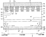
上記目的を達成するための請求項1では、IGBT素子(1a)を有するIGBT領域(1)と、FWD素子(2a)を有するFWD領域(2)とが共通の半導体基板(10)に形成されている半導体装置において、第1導電型のドリフト層(11)と、ドリフト層上に形成された第2導電型のベース層(12)と、ベース層の表層部であって、ベース層を挟んでドリフト層から離れた位置に形成され、ドリフト層よりも高不純物濃度とされた第1導電型のエミッタ領域(16)と、ドリフト層を挟んでベース層と反対側であって、IGBT領域に形成された第2導電型のコレクタ層(20)と、ドリフト層を挟んでベース層と反対側であって、FWD領域に形成され、コレクタ層と隣接する第1導電型のカソード層(21)と、ベース層と、コレクタ層およびカソード層との間に形成されたFS層(22)と、を有する半導体基板と、エミッタ領域とドリフト層との間に位置するベース層の表面に配置されたゲート絶縁膜(14)と、ゲート絶縁膜上に配置されたゲート電極(15)と、ベース層およびエミッタ領域と電気的に接続される第1電極(18)と、コレクタ層およびカソード層と電気的に接続される第2電極(23)と、を備え、FS層は、コレクタ層およびカソード層から離れて形成されており、FWD素子に順方向電流が流れている状態から当該電流を遮断してリカバリ状態となった際、FWD素子内の第1キャリアの一部がコレクタ層へと流れることにより、サージピーク電圧を小さくする量の第2キャリアが第2電極からコレクタ層を介してドリフト層に注入されるようにし、カソード層には、コレクタ層と離れた位置に、第2電極と電気的に接続される第2導電型のキャリア注入層(24)を形成する。 In order to achieve the above object, an IGBT region (1) having an IGBT element (1a) and an FWD region (2) having an FWD element (2a) are formed on a common semiconductor substrate (10). A first conductivity type drift layer (11), a second conductivity type base layer (12) formed on the drift layer, and a surface layer portion of the base layer, sandwiching the base layer The emitter region (16) of the first conductivity type formed at a position away from the drift layer and having a higher impurity concentration than the drift layer, and on the opposite side of the base layer across the drift layer and in the IGBT region The formed second conductivity type collector layer (20) and the first conductivity type cathode layer (21) formed in the FWD region on the opposite side of the base layer across the drift layer and adjacent to the collector layer And the base layer A semiconductor substrate having an FS layer (22) formed between the collector layer and the cathode layer, and a gate insulating film (14) disposed on the surface of the base layer located between the emitter region and the drift layer A gate electrode (15) disposed on the gate insulating film; a first electrode (18) electrically connected to the base layer and the emitter region; and a first electrode electrically connected to the collector layer and the cathode layer. The FS layer is formed apart from the collector layer and the cathode layer, and the current is cut off from the state in which the forward current is flowing through the FWD element to enter the recovery state. At this time, a part of the first carrier in the FWD element flows to the collector layer, so that an amount of the second carrier for reducing the surge peak voltage is injected from the second electrode to the drift layer through the collector layer. Is the way to, the cathode layer, at a position remote from the collector layer to form a second conductivity type carrier injection layer that are connected to the second electrode and the electrically (24).
Claims (4)
第1導電型のドリフト層(11)と、
前記ドリフト層上に形成された第2導電型のベース層(12)と、
前記ベース層の表層部であって、前記ベース層を挟んで前記ドリフト層から離れた位置に形成され、前記ドリフト層よりも高不純物濃度とされた第1導電型のエミッタ領域(16)と、
前記ドリフト層を挟んで前記ベース層と反対側であって、前記IGBT領域に形成された第2導電型のコレクタ層(20)と、
前記ドリフト層を挟んで前記ベース層と反対側であって、前記FWD領域に形成され、前記コレクタ層と隣接する第1導電型のカソード層(21)と、
前記ベース層と、前記コレクタ層および前記カソード層との間に形成されたフィールドストップ層(22)と、を有する前記半導体基板と、
前記エミッタ領域と前記ドリフト層との間に位置する前記ベース層の表面に配置されたゲート絶縁膜(14)と、
前記ゲート絶縁膜上に配置されたゲート電極(15)と、
前記ベース層および前記エミッタ領域と電気的に接続される第1電極(18)と、
前記コレクタ層および前記カソード層と電気的に接続される第2電極(23)と、を備え、
前記フィールドストップ層は、前記コレクタ層および前記カソード層から離れて形成されており、
前記FWD素子に順方向電流が流れている状態から当該電流を遮断してリカバリ状態となった際、前記FWD素子内の第1キャリアの一部が前記コレクタ層へと流れることにより、サージピーク電圧を小さくする量の第2キャリアが前記第2電極から前記コレクタ層を介して前記ドリフト層に注入され、
前記カソード層には、前記コレクタ層と離れた位置に、前記第2電極と電気的に接続される第2導電型のキャリア注入層(24)が形成されている半導体装置。 In a semiconductor device in which an IGBT region (1) having an IGBT element (1a) and an FWD region (2) having an FWD element (2a) are formed on a common semiconductor substrate (10),
A first conductivity type drift layer (11);
A second conductivity type base layer (12) formed on the drift layer;
A first conductivity type emitter region (16), which is a surface layer portion of the base layer, formed at a position away from the drift layer with the base layer interposed therebetween, and having a higher impurity concentration than the drift layer;
A second conductivity type collector layer (20) formed in the IGBT region on the opposite side of the base layer across the drift layer;
A cathode layer (21) of the first conductivity type formed on the FWD region on the opposite side of the drift layer and adjacent to the collector layer;
The semiconductor substrate comprising the base layer and a field stop layer (22) formed between the collector layer and the cathode layer;
A gate insulating film (14) disposed on a surface of the base layer located between the emitter region and the drift layer;
A gate electrode (15) disposed on the gate insulating film;
A first electrode (18) electrically connected to the base layer and the emitter region;
A second electrode (23) electrically connected to the collector layer and the cathode layer,
The field stop layer is formed away from the collector layer and the cathode layer;
When a forward current flows through the FWD element, the current is cut off and a recovery state is established, so that a part of the first carrier in the FWD element flows to the collector layer, thereby causing a surge peak voltage. Of the second carrier is injected from the second electrode into the drift layer through the collector layer ,
A semiconductor device in which a second conductivity type carrier injection layer (24) electrically connected to the second electrode is formed in the cathode layer at a position away from the collector layer .
Priority Applications (2)
| Application Number | Priority Date | Filing Date | Title |
|---|---|---|---|
| JP2017117072A JP2019004030A (en) | 2017-06-14 | 2017-06-14 | Semiconductor device |
| PCT/JP2018/020231 WO2018230312A1 (en) | 2017-06-14 | 2018-05-25 | Semiconductor device |
Applications Claiming Priority (1)
| Application Number | Priority Date | Filing Date | Title |
|---|---|---|---|
| JP2017117072A JP2019004030A (en) | 2017-06-14 | 2017-06-14 | Semiconductor device |
Publications (2)
| Publication Number | Publication Date |
|---|---|
| JP2019004030A JP2019004030A (en) | 2019-01-10 |
| JP2019004030A5 true JP2019004030A5 (en) | 2019-09-19 |
Family
ID=64660825
Family Applications (1)
| Application Number | Title | Priority Date | Filing Date |
|---|---|---|---|
| JP2017117072A Pending JP2019004030A (en) | 2017-06-14 | 2017-06-14 | Semiconductor device |
Country Status (2)
| Country | Link |
|---|---|
| JP (1) | JP2019004030A (en) |
| WO (1) | WO2018230312A1 (en) |
Families Citing this family (1)
| Publication number | Priority date | Publication date | Assignee | Title |
|---|---|---|---|---|
| CN113168588B (en) | 2019-01-15 | 2023-11-24 | 索尼集团公司 | Server and learning system |
Family Cites Families (10)
| Publication number | Priority date | Publication date | Assignee | Title |
|---|---|---|---|---|
| WO2007055352A1 (en) * | 2005-11-14 | 2007-05-18 | Fuji Electric Device Technology Co., Ltd. | Semiconductor device and method for manufacturing same |
| JP2012142537A (en) * | 2010-12-16 | 2012-07-26 | Mitsubishi Electric Corp | Insulated gate type bipolar transistor, and method of manufacturing the same |
| JP6011696B2 (en) * | 2011-07-27 | 2016-10-19 | トヨタ自動車株式会社 | Diode, semiconductor device and MOSFET |
| JP5737102B2 (en) * | 2011-09-19 | 2015-06-17 | 株式会社デンソー | Semiconductor device |
| JP5751125B2 (en) * | 2011-10-20 | 2015-07-22 | 株式会社デンソー | Semiconductor device |
| JP6119577B2 (en) * | 2013-11-26 | 2017-04-26 | 三菱電機株式会社 | Semiconductor device |
| JP6158123B2 (en) * | 2014-03-14 | 2017-07-05 | 株式会社東芝 | Semiconductor device |
| JP6261494B2 (en) * | 2014-12-03 | 2018-01-17 | 三菱電機株式会社 | Power semiconductor device |
| JP2015213193A (en) * | 2015-07-21 | 2015-11-26 | ルネサスエレクトロニクス株式会社 | Igbt |
| EP3154091A1 (en) * | 2015-10-07 | 2017-04-12 | ABB Technology AG | Reverse-conducting semiconductor device |
-
2017
- 2017-06-14 JP JP2017117072A patent/JP2019004030A/en active Pending
-
2018
- 2018-05-25 WO PCT/JP2018/020231 patent/WO2018230312A1/en active Application Filing
Similar Documents
| Publication | Publication Date | Title |
|---|---|---|
| JP2017208413A5 (en) | ||
| JP5967065B2 (en) | Semiconductor device | |
| US8928087B2 (en) | Semiconductor device | |
| JP2015135954A5 (en) | ||
| JP2014022708A5 (en) | ||
| JP6606007B2 (en) | Switching element | |
| JP2017212425A5 (en) | ||
| JP2019054070A5 (en) | ||
| JP2018148044A5 (en) | ||
| JP2019009308A5 (en) | ||
| US9620595B2 (en) | Semiconductor device | |
| US10304969B2 (en) | Semiconductor device | |
| JP2015144220A5 (en) | Semiconductor device | |
| JP6103038B2 (en) | Semiconductor device | |
| JP2019165180A5 (en) | ||
| JP6077309B2 (en) | Diode and semiconductor device incorporating diode | |
| JP2020088155A5 (en) | ||
| US9252212B2 (en) | Power semiconductor device | |
| JP2019004030A5 (en) | ||
| JP2014103352A (en) | Semiconductor device | |
| JP2017011319A5 (en) | ||
| JP2014187320A5 (en) | ||
| JP7029778B2 (en) | Semiconductor devices and their manufacturing methods | |
| JP2016149429A (en) | Reverse conducting IGBT | |
| JP2018186233A5 (en) |