JP2018537726A - Optical article provided in a form suitable for direct lamination, and method for manufacturing optical device - Google Patents
Optical article provided in a form suitable for direct lamination, and method for manufacturing optical device Download PDFInfo
- Publication number
- JP2018537726A JP2018537726A JP2018535241A JP2018535241A JP2018537726A JP 2018537726 A JP2018537726 A JP 2018537726A JP 2018535241 A JP2018535241 A JP 2018535241A JP 2018535241 A JP2018535241 A JP 2018535241A JP 2018537726 A JP2018537726 A JP 2018537726A
- Authority
- JP
- Japan
- Prior art keywords
- optical
- roughness
- optical article
- layer
- sensitive adhesive
- Prior art date
- Legal status (The legal status is an assumption and is not a legal conclusion. Google has not performed a legal analysis and makes no representation as to the accuracy of the status listed.)
- Granted
Links
Images

Classifications
-
- G—PHYSICS
- G02—OPTICS
- G02B—OPTICAL ELEMENTS, SYSTEMS OR APPARATUS
- G02B1/00—Optical elements characterised by the material of which they are made; Optical coatings for optical elements
- G02B1/04—Optical elements characterised by the material of which they are made; Optical coatings for optical elements made of organic materials, e.g. plastics
- G02B1/041—Lenses
-
- B—PERFORMING OPERATIONS; TRANSPORTING
- B29—WORKING OF PLASTICS; WORKING OF SUBSTANCES IN A PLASTIC STATE IN GENERAL
- B29D—PRODUCING PARTICULAR ARTICLES FROM PLASTICS OR FROM SUBSTANCES IN A PLASTIC STATE
- B29D11/00—Producing optical elements, e.g. lenses or prisms
- B29D11/00009—Production of simple or compound lenses
-
- B—PERFORMING OPERATIONS; TRANSPORTING
- B29—WORKING OF PLASTICS; WORKING OF SUBSTANCES IN A PLASTIC STATE IN GENERAL
- B29D—PRODUCING PARTICULAR ARTICLES FROM PLASTICS OR FROM SUBSTANCES IN A PLASTIC STATE
- B29D11/00—Producing optical elements, e.g. lenses or prisms
- B29D11/0073—Optical laminates
-
- B—PERFORMING OPERATIONS; TRANSPORTING
- B29—WORKING OF PLASTICS; WORKING OF SUBSTANCES IN A PLASTIC STATE IN GENERAL
- B29D—PRODUCING PARTICULAR ARTICLES FROM PLASTICS OR FROM SUBSTANCES IN A PLASTIC STATE
- B29D11/00—Producing optical elements, e.g. lenses or prisms
- B29D11/00865—Applying coatings; tinting; colouring
-
- B—PERFORMING OPERATIONS; TRANSPORTING
- B29—WORKING OF PLASTICS; WORKING OF SUBSTANCES IN A PLASTIC STATE IN GENERAL
- B29D—PRODUCING PARTICULAR ARTICLES FROM PLASTICS OR FROM SUBSTANCES IN A PLASTIC STATE
- B29D11/00—Producing optical elements, e.g. lenses or prisms
- B29D11/00951—Measuring, controlling or regulating
- B29D11/00961—Measuring, controlling or regulating using microprocessors or computers
-
- G—PHYSICS
- G02—OPTICS
- G02C—SPECTACLES; SUNGLASSES OR GOGGLES INSOFAR AS THEY HAVE THE SAME FEATURES AS SPECTACLES; CONTACT LENSES
- G02C2202/00—Generic optical aspects applicable to one or more of the subgroups of G02C7/00
- G02C2202/16—Laminated or compound lenses
Landscapes
- Engineering & Computer Science (AREA)
- Health & Medical Sciences (AREA)
- Manufacturing & Machinery (AREA)
- Ophthalmology & Optometry (AREA)
- Mechanical Engineering (AREA)
- Physics & Mathematics (AREA)
- General Physics & Mathematics (AREA)
- Optics & Photonics (AREA)
- Microelectronics & Electronic Packaging (AREA)
- Laminated Bodies (AREA)
- Lining Or Joining Of Plastics Or The Like (AREA)
- Testing Of Optical Devices Or Fibers (AREA)
- Optical Filters (AREA)
- Surface Treatment Of Optical Elements (AREA)
- Polarising Elements (AREA)
Abstract
感圧接着剤層及び熱可塑性薄膜の同時ラミネーションに適した形態で提供される光学物品であって、凸状及び凹状光学表面を含み、凸状及び/又は凹状光学表面は、感圧接着剤であって、その上に熱可塑性薄膜が配置されることを意図される、感圧接着剤を受け入れることを意図された受け入れ表面であり、前記受け入れ表面は、0.01μm以上且つ0.3μm以下の算術平均プロファイル粗度を有し、及び/又は前記受け入れ表面は、0.2°以上且つ1.2°以下のプロファイル粗度二乗平均平方根勾配を有する、光学物品。前記光学物品を使用して光学装置を製造する方法。An optical article provided in a form suitable for simultaneous lamination of a pressure sensitive adhesive layer and a thermoplastic thin film, comprising a convex and concave optical surface, wherein the convex and / or concave optical surface is a pressure sensitive adhesive. A receiving surface intended to receive a pressure sensitive adhesive on which a thermoplastic film is intended to be disposed, the receiving surface being not less than 0.01 μm and not more than 0.3 μm An optical article having an arithmetic mean profile roughness and / or wherein said receiving surface has a profile roughness root mean square slope of not less than 0.2 ° and not more than 1.2 °. A method of manufacturing an optical device using the optical article.
Description
本発明は、概して、例えばメガネレンズなどの光学物品の分野に関する。更に詳しくは、本発明は、直接的なラミネーションに適した形態で提供される光学物品に関する。本発明は、前記光学物品を使用して光学装置を製造する方法にも関する。 The present invention relates generally to the field of optical articles such as eyeglass lenses. More particularly, the present invention relates to an optical article provided in a form suitable for direct lamination. The present invention also relates to a method of manufacturing an optical device using the optical article.
光学物品は、例えば、可視光などの光の挙動及び特性を伴う。光学物品は、少なくとも1つの光学表面を含み、及び少なくとも前記光学表面との間の光のやり取りの結果として光路が得られる。光学物品は、複数の光学表面を含み得、及びこれらの光学表面との間且つ前記光学表面を分離している1つの材料(又は複数の材料)との間の光のやり取りの結果として光路が得られる。 Optical articles are associated with the behavior and characteristics of light, such as, for example, visible light. The optical article includes at least one optical surface, and an optical path is obtained as a result of at least light exchange with the optical surface. An optical article may include a plurality of optical surfaces, and the optical path as a result of the exchange of light between these optical surfaces and a material (or materials) separating the optical surfaces. can get.
光学物品の1つとして、レンズが広く使用されている。レンズは、屈折を通じて光ビームの焦点に影響を及ぼす透過性の光学物品である。メガネレンズは、単一の材料片からなるレンズである。 Lenses are widely used as one of optical articles. A lens is a transmissive optical article that affects the focus of a light beam through refraction. The spectacle lens is a lens made of a single piece of material.
光学物品の光学表面上に層を提供するニーズが存在する。前記層は、光学物品の性能を改善するように設計される。これらは、例えば、光学表面の表面品質を変更し得、光学物品の色を変更し得、光学物品を磨滅から保護し得、反射防止機能を追加し得、且つ更なる層及び又は被覆を追加するための基材であり得る。 There is a need to provide a layer on the optical surface of an optical article. The layer is designed to improve the performance of the optical article. These can, for example, change the surface quality of the optical surface, change the color of the optical article, protect the optical article from abrasion, add anti-reflective functions, and add additional layers and / or coatings It can be a substrate for
従って、少なくとも1つの層を受け入れるのに適した形態である光学物品を提供するニーズが存在する。 Accordingly, there is a need to provide an optical article that is in a form suitable for receiving at least one layer.
この目的のために、本発明の対象は、感圧接着剤層及び熱可塑性薄膜の同時ラミネーションに適した形態で提供される光学物品であって、互いに対向する凸状及び凹状光学表面を含み、凸状及び/又は凹状光学表面は、感圧接着剤であって、その上に熱可塑性薄膜が配置されることが意図される、感圧接着剤を受け入れることを意図された()受け入れ表面であり、前記受け入れ表面は、0.01μm以上且つ0.3μm以下の算術平均プロファイル粗度Raを有し、及び/又は前記受け入れ表面は、0.2°以上且つ1.2°以下のプロファイル粗度二乗平均平方根勾配Rdqを有する、光学物品である。 For this purpose, the subject of the present invention is an optical article provided in a form suitable for simultaneous lamination of a pressure sensitive adhesive layer and a thermoplastic thin film, comprising convex and concave optical surfaces facing each other, Convex and / or concave optical surfaces are pressure sensitive adhesives that are intended to accept pressure sensitive adhesives on which a thermoplastic film is intended to be disposed And the receiving surface has an arithmetic average profile roughness Ra of 0.01 μm or more and 0.3 μm or less, and / or the receiving surface has a profile roughness of 0.2 ° or more and 1.2 ° or less. An optical article having a root mean square slope Rdq.
「受け入れ表面は、0.01μm以上且つ0.3μm以下の算術平均プロファイル粗度Raを有し、及び/又は前記受け入れ表面は、0.2°以上且つ1.2°以下のプロファイル粗度二乗平均平方根勾配Rdqを有する」という条件は、以下では「選択された粗度特徴」と呼称される。一実施形態では、算術平均プロファイル粗度Raは、0.02μm以上又は更に0.03μm超である。 “The receiving surface has an arithmetic average profile roughness Ra of 0.01 μm or more and 0.3 μm or less, and / or the receiving surface has a profile roughness mean square of 0.2 ° or more and 1.2 ° or less The condition “having a square root slope Rdq” will be referred to below as “selected roughness features”. In one embodiment, the arithmetic average profile roughness Ra is greater than or equal to 0.02 μm or even greater than 0.03 μm.
一実施形態によれば、選択された粗度特徴は、受け入れ表面が0.01μm以上且つ0.3μm以下の算術平均プロファイル粗度を有するようなものである。 According to one embodiment, the selected roughness feature is such that the receiving surface has an arithmetic average profile roughness of 0.01 μm or more and 0.3 μm or less.
上記のものと組み合わせられ得る別の実施形態によれば、選択された粗度特徴は、受け入れ表面が0.2°以上且つ1.2°以下のプロファイル粗度二乗平均平方根勾配Rdqを有するようなものである。 According to another embodiment that may be combined with the above, the selected roughness feature is such that the receiving surface has a profile roughness root mean square slope Rdq of 0.2 ° to 1.2 °. Is.
本発明者らは、選択された粗度特徴が、感圧接着剤層及び熱可塑性薄膜を光学物品の受け入れ表面上に直接ラミネートした後に改善された特徴を取得するのに適することを実証した。 The inventors have demonstrated that the selected roughness characteristics are suitable for obtaining improved characteristics after laminating the pressure sensitive adhesive layer and the thermoplastic film directly onto the receiving surface of the optical article.
従って、本発明の光学物品は、例えば、感圧接着剤層が前記光学物品の受け入れ表面上に接着され、及び熱可塑性薄膜が感圧接着剤層上に配置される場合、光学装置を更に製造するために有利である。 Thus, the optical article of the present invention further produces an optical device when, for example, a pressure sensitive adhesive layer is adhered on the receiving surface of the optical article and a thermoplastic thin film is disposed on the pressure sensitive adhesive layer. It is advantageous to
本発明によれば、光学物品は、互いに対向し、且つ材料によって分離された凸状及び凹状光学表面を含む。一実施形態によれば、前記材料は透明材料である。 In accordance with the present invention, an optical article includes convex and concave optical surfaces facing each other and separated by material. According to one embodiment, the material is a transparent material.
通常の定義に従って、
・算術平均プロファイル粗度Raは、平均ラインからの粗度プロファイルの垂直方向の逸脱に基づいて表面の特徴を判定する振幅パラメータである。算術平均プロファイル粗度Raは、粗度プロファイル縦座標の絶対値の算術平均値である。
・粗度二乗平均平方根勾配Rdqは、粗度プロファイルの勾配の特性を記述する勾配パラメータである。粗度二乗平均平方根勾配Rdqは、サンプリング長内におけるプロファイルの二乗平均平方根勾配である。
According to the usual definition
Arithmetic mean profile roughness Ra is an amplitude parameter that determines surface features based on the vertical deviation of the roughness profile from the mean line. The arithmetic average profile roughness Ra is an arithmetic average value of absolute values of the roughness profile ordinate.
The roughness root mean square slope Rdq is a slope parameter that describes the slope characteristics of the roughness profile. The roughness root mean square slope Rdq is the root mean square slope of the profile within the sampling length.
すべての技術的に価値を有する実施形態に従って組み合わせることができる本発明の光学物品の異なる実施形態によれば、
− 同時にラミネートされることを意図された感圧接着剤層及び熱可塑性薄膜は、感圧接着剤層が熱可塑性薄膜上に配置される多層薄膜の形態であり、
− 受け入れ表面は、以下の式:
RSM≧min(0.64×Ra;0.58×Ra+0.007)
による、RSMと呼称されるピーク間の平均間隔を有し、ここで、「min(x;y)」は、xとyとの間の最小値の選択を指し、
− 受け入れ表面は、以下の式:RSM≧0.64×Raによる、RSMと呼称されるピーク間の平均間隔を有し、
− 受け入れ表面は、以下の式:RSM≧0.58×Ra+0.007による、RSMと呼称されるピーク間の平均間隔を有する。
According to different embodiments of the optical article of the present invention that can be combined according to all technically valuable embodiments,
The pressure sensitive adhesive layer and the thermoplastic thin film intended to be laminated at the same time are in the form of a multilayer thin film in which the pressure sensitive adhesive layer is disposed on the thermoplastic thin film;
The receiving surface has the following formula:
RSM ≧ min (0.64 × Ra; 0.58 × Ra + 0.007)
With an average spacing between peaks called RSM, where “min (x; y)” refers to the selection of the minimum value between x and y,
The receiving surface has an average spacing between peaks called RSM according to the following formula: RSM ≧ 0.64 × Ra;
The receiving surface has an average spacing between peaks, referred to as RSM, according to the following formula: RSM ≧ 0.58 × Ra + 0.007.
本発明は、選択された粗度特徴を有する光学物品、感圧接着剤層、及び熱可塑性薄膜を含む光学装置であって、同時ラミネーションにより、感圧接着剤層は、光学物品の受け入れ表面上に接着され、及び熱可塑性薄膜は、感圧接着剤層上に配置される、光学装置も対象とする。 The present invention is an optical device comprising an optical article having a selected roughness characteristic, a pressure sensitive adhesive layer, and a thermoplastic thin film, wherein by simultaneous lamination, the pressure sensitive adhesive layer is on the receiving surface of the optical article. Also contemplated are optical devices, wherein the thermoplastic film is disposed on the pressure sensitive adhesive layer.
同時にラミネートされた後、感圧接着剤層及び熱可塑性薄膜は分離することができないことを理解されたい。 It should be understood that the pressure sensitive adhesive layer and the thermoplastic film cannot be separated after being simultaneously laminated.
一実施形態によれば、感圧接着剤層の厚さは、20μm以上且つ250μm以下、例えば25μm以上且つ/又は75μm以下である。 According to one embodiment, the thickness of the pressure sensitive adhesive layer is not less than 20 μm and not more than 250 μm, for example not less than 25 μm and / or not more than 75 μm.
一実施形態によれば、熱可塑性薄膜の厚さは、30μm以上且つ500μm以下、例えば80μm以上且つ/又は200μm以下である。 According to one embodiment, the thickness of the thermoplastic thin film is not less than 30 μm and not more than 500 μm, for example not less than 80 μm and / or not more than 200 μm.
本発明は、光学装置を製造する方法であって、
・選択された粗度特徴を有する光学物品を提供するステップと、
・感圧接着剤層及び熱可塑性薄膜を提供するステップと、
・感圧接着剤層が前記受け入れ表面上に接着し、及び熱可塑性薄膜が感圧接着剤上に配置されるように、感圧接着剤層及び熱可塑性薄膜を光学物品の受け入れ表面上に直接ラミネートするステップと
を含む方法も対象とする。
The present invention is a method of manufacturing an optical device comprising:
Providing an optical article having selected roughness characteristics;
Providing a pressure sensitive adhesive layer and a thermoplastic film;
The pressure sensitive adhesive layer and the thermoplastic film are directly on the receiving surface of the optical article so that the pressure sensitive adhesive layer adheres to the receiving surface and the thermoplastic film is disposed on the pressure sensitive adhesive; Also included is a method comprising a laminating step.
すべての技術的に価値を有する実施形態に従って組み合わせられ得る本発明の製造方法の異なる実施形態によれば、
− 提供された感圧接着剤及び熱可塑性薄膜は、感圧接着剤層が熱可塑性薄膜上に配置される多層薄膜の形態であり、
− 熱可塑性薄膜は、被覆を更に含む構造化薄膜の一部分であり、前記被覆は、優先的に、感圧接着剤層と接触することを意図された熱可塑性薄膜の別の面とは反対側の熱可塑性薄膜の面上に配置され、更に場合により、被覆は、熱可塑性薄膜と感圧層との間に存在し得、この場合、前記被覆は、熱可塑性薄膜、ハードコート層、下塗層、フォトクロミック層、分極層、液晶層、エレクトロクロミック層、静電防止層、反射防止層などの干渉性積層体、ミラー若しくは反射性層又は可視スペクトルの一部の部分に反射性を有する層、着色層、1つ又は複数の波長範囲をフィルタリングする選択的フィルタ、防汚層、防曇層、抗雨層、疎水層、或いはこれらの組合せからなるリスト内で選択され、
− 前記製造方法は、感圧接着剤層及び熱可塑性薄膜が予めラミネートされている光学装置の表面上に少なくとも補助層を提供するステップを更に含み、この場合、前記少なくとも1つの補助層は、熱可塑性薄膜、ハードコート層、下塗層、フォトクロミック層、分極層、液晶層、エレクトロクロミック層、静電防止層、反射防止層などの干渉性積層体、ミラー若しくは反射性層又は可視スペクトルの一部の部分に反射性を有する層、着色層、1つ又は複数の波長範囲をフィルタリングする選択的フィルタ、防汚層、防曇層、抗雨層、疎水層、或いはこれらの組合せからなるリスト内で選択され、
− 前記製造方法では、熱可塑性薄膜は、被覆を更に含む構造化薄膜の一部分であり、及び方法は、感圧接着剤層及び熱可塑性薄膜が予めラミネートされている光学装置の表面上に少なくとも1つの補助層を提供するステップを更に含み、
− 前記製造方法では、熱可塑性薄膜又は感圧層のいずれかは、少なくとも染料、顔料、吸収剤、フォトクロミック染料の追加又は存在により、更なる光学特性を含み、
− 光学物品は、粗化ステップ及び微細化ステップの少なくとも1つと、粗化ステップ、微細化ステップ、及び粗さ消去ステップから選択される2つ以下のステップとを含む半完成光学物品の機械加工プロセスにより、受け入れ表面を提供するために半完成光学物品から予め製造され、一実施形態によれば、半完成光学物品の機械加工プロセスは、粗さ消去ステップのみを含み、一実施形態によれば、半完成光学物品の機械加工プロセスは、粗化ステップのみを含み、
− 前記製造方法は、制御ステップ及び意思決定ステップによって後続される、互いに対向する凸状及び凹状光学表面を含む供給された光学物品を提供する予備ステップを含み、この場合、
・制御ステップは、受け入れ表面となることを意図される供給された光学物品の表面の粗度を判定するステップを含み、
・意思決定ステップは、
i.前記光学表面の予め判定された粗度を、選択された粗度特徴を有する光学物品の受け入れ表面の1つと比較するサブステップと、
ii.選択された粗度特徴に対応する粗度要件が満たされる場合、供給された光学物品を製造方法の提供ステップに提供し、且つ選択された粗度特徴に対応する粗度要件が満たされない場合、供給された光学物品を補完ステップに提供するサブステップと
を含み、
− 受け入れ表面となることを意図される表面の粗度を判定するステップは、前記表面の粗度を計測するステップと、前記表面の事前の製造データに基づいて前記表面の粗度を推定するステップと、前記表面を既知の粗度の表面と比較するステップとからなるリスト内で選択される方法に従って実施され、
− 補完ステップは、供給された光学物品を拒絶するステップと、供給された光学物品を製造方法の提供ステップに提供するために、前記表面の粗度が、機械加工ステップ後、選択された粗度特徴を満たすように、受け入れ表面となることを意図される表面を更に前記機械加工するステップとのリスト内で選択され、一実施形態によれば、受け入れ表面となることを意図される表面を更に機械加工するステップは、フラッシュ研磨ステップからなる。
According to different embodiments of the production method of the present invention, which can be combined according to all technically valuable embodiments,
The provided pressure sensitive adhesive and thermoplastic film is in the form of a multilayer film in which the pressure sensitive adhesive layer is disposed on the thermoplastic film;
The thermoplastic film is part of a structured film further comprising a coating, said coating preferentially opposite the other side of the thermoplastic film intended to contact the pressure sensitive adhesive layer Further, in some cases, a coating may be present between the thermoplastic thin film and the pressure-sensitive layer, in which case the coating comprises the thermoplastic thin film, the hard coat layer, the primer layer. Layer, photochromic layer, polarization layer, liquid crystal layer, electrochromic layer, anti-reflection layer, anti-reflection layer, and other coherent laminates, mirrors or reflective layers, or layers having reflectivity in part of the visible spectrum Selected from a list consisting of a colored layer, a selective filter that filters one or more wavelength ranges, an antifouling layer, an antifogging layer, an anti-rain layer, a hydrophobic layer, or combinations thereof;
The manufacturing method further comprises providing at least an auxiliary layer on the surface of the optical device on which the pressure sensitive adhesive layer and the thermoplastic thin film have been pre-laminated, wherein the at least one auxiliary layer comprises a heat Interferometric laminates such as plastic thin films, hard coat layers, undercoat layers, photochromic layers, polarization layers, liquid crystal layers, electrochromic layers, antistatic layers, antireflection layers, mirrors or reflective layers, or parts of the visible spectrum In a list of reflective layers, colored layers, selective filters that filter one or more wavelength ranges, antifouling layers, antifogging layers, rainproof layers, hydrophobic layers, or combinations thereof Selected
-In said manufacturing method, the thermoplastic thin film is part of a structured thin film further comprising a coating, and the method comprises at least one on the surface of the optical device on which the pressure sensitive adhesive layer and the thermoplastic thin film have been pre-laminated. Further comprising providing two auxiliary layers,
-In the production method, either the thermoplastic thin film or the pressure sensitive layer comprises further optical properties, at least by the addition or presence of dyes, pigments, absorbers, photochromic dyes
The optical article is a semi-finished optical article machining process comprising at least one of a roughening step and a finening step and no more than two steps selected from a roughening step, a finening step and a roughness erasing step Pre-manufactured from a semi-finished optical article to provide a receiving surface, according to one embodiment, the machining process of the semi-finished optical article includes only a roughness elimination step, according to one embodiment The machining process of the semi-finished optical article includes only a roughening step,
The manufacturing method comprises a preliminary step of providing a supplied optical article comprising convex and concave optical surfaces facing each other, followed by a control step and a decision-making step, wherein
The controlling step comprises determining the roughness of the surface of the supplied optical article intended to be the receiving surface;
・ The decision-making step is
i. Comparing the predetermined roughness of the optical surface with one of the receiving surfaces of an optical article having a selected roughness feature;
ii. If the roughness requirement corresponding to the selected roughness feature is met, the supplied optical article is provided to the providing step of the manufacturing method, and if the roughness requirement corresponding to the selected roughness feature is not met, Providing a supplied optical article to a complementary step; and
The step of determining the roughness of the surface intended to be the receiving surface comprises measuring the roughness of the surface and estimating the roughness of the surface based on prior manufacturing data of the surface And according to a method selected in a list consisting of comparing the surface with a surface of known roughness
The complementing step comprises the steps of rejecting the supplied optical article and providing the supplied optical article to the manufacturing method providing step, wherein the roughness of the surface is selected after the machining step; In order to satisfy the characteristics, a surface intended to be a receiving surface is further selected in the list with the step of machining, and according to one embodiment, a surface intended to be a receiving surface is further selected. The machining step comprises a flash polishing step.
以下では、添付図面を参照して例について説明する。 In the following, examples will be described with reference to the accompanying drawings.
図中の要素は、簡潔性及びわかりやすさを目的として示されており、且つ必ずしも正確な縮尺で描画されていない。例えば、図中のいくつかの要素の寸法は、本発明の実施形態の理解の改善を支援するために他の要素との関係で誇張されている場合がある。 Elements in the figures are shown for simplicity and clarity and are not necessarily drawn to scale. For example, the dimensions of some elements in the figures may be exaggerated in relation to other elements to help improve understanding of embodiments of the invention.
添付の図では、同一の参照符号は同一の部分に対応する。 In the accompanying drawings, the same reference numerals correspond to the same parts.
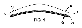
図1は、光学物品10と、感圧接着剤層20と、熱可塑性薄膜30とを含む光学装置1を示す。前記光学物品10は、互いに対向する凸状光学表面11及び凹状光学表面12を含む。一例によれば、光学装置1は、眼科メガネレンズである。
FIG. 1 shows an optical device 1 that includes an
本発明の用語法によれば、「薄膜」は、単独で使用された場合、材料の単一の層を意味する。一例によれば、薄膜は、機能的な薄膜であり、一例によれば、薄膜は、自己支持型である。 According to the terminology of the present invention, “thin film”, when used alone, means a single layer of material. According to one example, the thin film is a functional thin film, and according to one example, the thin film is self-supporting.
一例によれば、熱可塑性薄膜30は、セルローストリアセテート(TAC)薄膜である。
According to one example, the thermoplastic
一例によれば、感圧接着剤層20及び熱可塑性薄膜30は、多層薄膜として組み立てられる。本発明の枠内では、「多層薄膜」は、固有の階層化構造の一部分である感圧接着剤層及び熱可塑性薄膜を意味し、この場合、感圧接着剤層は、熱可塑性薄膜上に配置される。
According to one example, the pressure sensitive
本発明の用語法によれば、「構造化薄膜」は、階層化構造の一部分である材料の複数の薄膜又は層を意味する。一例によれば、構造化薄膜は、それ自体により自己支持されていない状態において、第1材料薄膜と、1つに接着された同一若しくは異なる特性を有する1つ若しくは複数の個々の薄膜層、又は同一若しくは異なる特性を有する更なる層とを含む階層化構造である。本発明の一実施形態によれば、熱可塑性薄膜は、被覆を更に含む構造化薄膜の一部分であり、前記被覆は、優先的に、感圧接着剤層と接触することを意図された熱可塑性薄膜の別の面とは反対側の熱可塑性薄膜の面上に配置される。 According to the terminology of the present invention, “structured thin film” means a plurality of thin films or layers of material that are part of a layered structure. According to one example, the structured thin film is not self-supported by itself, and the first material thin film and one or more individual thin film layers having the same or different properties bonded together, or It is a hierarchical structure including further layers having the same or different characteristics. According to an embodiment of the present invention, the thermoplastic film is part of a structured film further comprising a coating, said coating preferentially being in contact with the pressure sensitive adhesive layer. It is disposed on the surface of the thermoplastic film opposite the other surface of the film.
レンズなどの光学物品は、例えば、望ましい形状に成形されると共に、例えば、成型、及び/又は研削、及び/又は研磨された例えばガラス又はプラスチック材料などの材料から製造される。一実施形態によれば、前記材料は透明材料である。 Optical articles, such as lenses, are, for example, fabricated from materials such as glass or plastic materials that are molded into a desired shape and, for example, molded and / or ground and / or polished. According to one embodiment, the material is a transparent material.
一実施形態によれば、レンズなどの光学物品は、「半完成」品とも呼称されるブランクから機械加工される。レンズ、即ち、メガネレンズ用のブランクは、例えば、完成した前部表面と、着用者用の処方仕様などの光学仕様を得るために、通常、「表面処理」と呼称されるプロセスを通じた作業(表面加工とも呼称される)を依然として必要としている後部表面とを有する「厚いレンズ」であってもよい。これは、光学仕様を得るように、前部表面と後部表面との両方が作業(又は表面加工)を必要としている「厚いレンズ」であってもよい。 According to one embodiment, an optical article, such as a lens, is machined from a blank, also referred to as a “semi-finished” product. Lenses, i.e., eyeglass lens blanks, work through a process commonly referred to as "surface treatment" to obtain, for example, a finished front surface and optical specifications such as prescription specifications for the wearer ( It may also be a “thick lens” with a rear surface that still requires surface processing (also called surface processing). This may be a “thick lens” where both the front and back surfaces require work (or surface processing) to obtain optical specifications.
光学表面の表面処理は、以下の一般的に使用される機械加工ステップの1つ又はいくつかにより実施することができる。 Surface treatment of the optical surface can be performed by one or several of the following commonly used machining steps.
・その望ましい厚さ及び曲率半径を光学物品に付与するために、ダイヤモンド砥石又はブレードによって光学物品の材料をミリングするステップからなる「粗化」。粗化後、光学表面は、そのほとんどが最終的な形状を得ているが、依然として粗く半透明な表面を有し、粗化は、以下の方法の少なくとも1つを使用して実行することができる。
○その望ましい厚さ及び曲率半径を光学物品に付与するために、砥石車(通常、接合されたダイヤアモンドの微細粒子から製造されている)によって光学物品の材料を研削するステップからなる「研削」。
○その望ましい厚さ及び曲率半径を光学物品に付与するために、回転駆動された切削ツールによって光学物品の材料を除去するステップからなる「ミリング」。
“Roughening” consisting of milling the material of the optical article with a diamond wheel or blade in order to impart the desired thickness and radius of curvature to the optical article. After roughening, the optical surface mostly has the final shape, but still has a rough and translucent surface, and the roughening can be performed using at least one of the following methods: it can.
“Grinding” consisting of grinding the material of the optical article with a grinding wheel (usually made from fine particles of bonded diamond diamond) to impart to the optical article its desired thickness and radius of curvature .
O "Milling" consisting of removing the material of the optical article with a rotationally driven cutting tool in order to impart its desired thickness and radius of curvature to the optical article.
・その曲率半径を変更することなく光学表面の粒を微細化するステップからなる、「スムージング」又は「微細切削」とも呼称される「微細化」。これは、十分な表面特性、即ち、ミクロンレベル未満の表面下損傷や小さい欠陥のうねりを有するレンズに対してその望ましい厚さ及び曲率半径を付与するように、過剰な材料を除去するステップを含む。一実施形態によれば、堅固に保持された光学物品は、研磨パッド又はディスクが装着されたツールと接触されており、ツールの曲率半径は、求められるレンズのものと同一である。光学物品及びツールは、潤滑液により作動し且つ冷却される。別の実施形態によれば、粗化ステップよりも微細なペースを伴う、欧州特許出願公開第2724815A1号明細書に示されているものなどの旋盤の動作では、表面をミリングするために単結晶ダイヤモンドブレードを使用することができる。数分間にわたって継続する微細化動作の終了時点において、光学物品は、表面の形状が光学物品について判定された光学補正をもたらすものにほぼ等しくなるように、必要とされる正確な厚さ及び曲率を有するものの、表面は、依然として完全に滑らか且つ透明な状態ではない。プロセスに応じて、微細化ステップは、以下の1つ又は複数のサブステップを含むことができる。 “Refining”, also referred to as “smoothing” or “microcutting”, comprising the steps of refining the grains of the optical surface without changing its radius of curvature. This includes removing excess material to provide sufficient surface properties, i.e., the desired thickness and radius of curvature for lenses with sub-micron level subsurface damage and small defect undulations. . According to one embodiment, the rigidly held optical article is in contact with a tool fitted with a polishing pad or disk, and the radius of curvature of the tool is the same as that of the required lens. Optical articles and tools are actuated and cooled by a lubricating liquid. According to another embodiment, the operation of a lathe, such as that shown in EP 2724815 A1, with a finer pace than the roughening step, a single crystal diamond to mill the surface A blade can be used. At the end of the micronization operation that lasts for several minutes, the optical article has the exact thickness and curvature required so that the surface shape is approximately equal to that resulting in the optical correction determined for the optical article. However, the surface is still not completely smooth and transparent. Depending on the process, the miniaturization step can include one or more of the following sub-steps.
・「研磨」とも呼称される粗さ消去ステップは、透明性を光学物品に付与するために使用される仕上げ動作である。この動作は、粗化及び仕上げステップに起因する痕跡を除去し、これにより、ダイヤモンドブレードによって形成された溝のスムージングを可能にする。これは、表面下損傷を除去するために全体表面上で数マイクロメートルの材料を除去するステップを含み、且つ残っている微細切削のうねり及び粗さをフィルタリングする。この段階は、表面及び研磨環境(ミクロンレベルの砥粒を含むスラリ)内の表面に対してそれ自体を準拠させるように適合されたソフトな研磨ツール間で相対運動を適用するステップを含み。従って、これは、多くの場合、ソフトな研磨ディスクと、非常に微細な粒を有する研磨液とを使用し、且つ従って、多くの場合に「ソフト研磨ステップ」と呼称される。ソフト研磨ステップでは、研磨された表面の曲率の変更は不可能である。換言すれば、これは、光学物品の表面の光学機能を定義する波長における表面の形状に対して影響を及ぼすことができない。 The roughness elimination step, also called “polishing”, is a finishing operation used to impart transparency to the optical article. This action removes traces due to the roughening and finishing steps, thereby enabling the smoothing of the grooves formed by the diamond blade. This includes removing a few micrometers of material on the entire surface to remove subsurface damage and filtering the remaining fine cutting waviness and roughness. This stage includes applying relative motion between the soft polishing tool adapted to conform itself to the surface and the surface in the polishing environment (a slurry containing micron level abrasive grains). Thus, this often uses a soft abrasive disc and a polishing fluid having very fine grains and is therefore often referred to as a “soft polish step”. In the soft polishing step, it is impossible to change the curvature of the polished surface. In other words, this cannot affect the shape of the surface at a wavelength that defines the optical function of the surface of the optical article.
現時点の光学表面は、多くの場合、上述の3つの機械加工ステップを連続的に実施することによって製造される。但し、他の製造方法が実施されてもよい。 Current optical surfaces are often manufactured by sequentially performing the three machining steps described above. However, other manufacturing methods may be implemented.
図1では、凹状光学表面12に、前記表面に接触する感圧接着剤層20と、感圧接着剤層上に配置された熱可塑性薄膜30とが提供される。本発明の枠内では、光学表面12は「受け入れ表面」と呼称されており、その理由は、これが、熱可塑性薄膜がその上に配置されることを意図された感圧接着剤を受け入れることを意図されるからである。感圧接着剤層20及び熱可塑性薄膜30は、受け入れ表面12上にラミネートされる。
In FIG. 1, a concave
ラミネーションは、1つに接合された複数の層を含み部分を製造する周知の技法である。従って、これは、表面上でこれらの層を形成するように、前記層を前記表面上に転送し且つ糊付けするステップを含み。ラミネーションは、複数の層を1つに圧縮及び圧延することによって得ることができる。ラミネーションステップでは、圧力が層上に印加される。国際公開第2006/105999号パンフレットは、薄膜を、本発明を実施するのに適し得る眼科レンズ上にラミネートするための装置を開示している。一例によれば、層上における圧力は、1バール以上であり、例えば、圧力は2バール〜3バールであり、一例によれば、圧力は30秒〜2分の期間にわたって層上に印加される。 Lamination is a well-known technique for manufacturing a part that includes multiple layers joined together. Thus, this involves transferring and gluing the layers onto the surface to form these layers on the surface. Lamination can be obtained by compressing and rolling a plurality of layers into one. In the lamination step, pressure is applied over the layer. WO 2006/105999 discloses an apparatus for laminating a thin film onto an ophthalmic lens that may be suitable for practicing the present invention. According to one example, the pressure on the layer is 1 bar or more, for example, the pressure is 2 to 3 bar, and according to one example, the pressure is applied on the layer over a period of 30 seconds to 2 minutes. .
「PSA」とも呼称される感圧接着剤は、光学物品の光屈折特性を保持しつつ、薄膜を光学物品の表面上に配置するために光学装置の分野で既知である。このタイプの接着剤材料に関与する接着のメカニズムは、化学的な接合を伴わず、PSA材料の特定の粘弾性特性を活用することに留意されたい。それぞれのPSA処方に固有のこれらの特性は、接着の境界面におけるファンデルワールス静電相互作用の確立を可能にする。これは、圧力の印加により、PSAが固体材料との接触状態に配置された場合に生成されるものである。 Pressure sensitive adhesives, also referred to as “PSA”, are known in the field of optical devices to place a thin film on the surface of an optical article while retaining the photorefractive properties of the optical article. It should be noted that the adhesion mechanism involved with this type of adhesive material does not involve chemical bonding and exploits the specific viscoelastic properties of the PSA material. These properties unique to each PSA formulation allow the establishment of van der Waals electrostatic interactions at the interface of the bond. This is generated when the PSA is placed in contact with the solid material by the application of pressure.
いくつかの感圧接着剤材料を使用することができる。有利には、使用される感圧接着剤材料は、ポリアクリレートベース、スチレンに基づいたコポリマー、及び天然ゴムを含む混合物を含む群から選択される。更に詳しくは、ポリアクリレートやポリメタクリレートに基づいた一般的な組成を有するPSA、エチレンビニルアセテート、エチレンエチルアクリレート、エチレンエチルメタクリレートなどに基づいたエチレン系コポリマー、シリコーン、ポリウレタン、ブタジエンスチレン、ポリブタジエン、ポリイソプレン、ポリプロピレン、ポリイソブチレンを含む、合成ゴム及びエラストマのベースを有するPSA、亜硝酸塩又はアクリロニトリルを含みポリマーに基づいたPSA、ポリクロロプレンに基づいたPSA、ポリスチレン、ポリエチレン、ポリプロピレン、ポリイソプレン、ポリブタジエンを含みブロックコポリマーに基づいたPSA、ポリビニルピロリドン及びビニルピロリドンコポリマーに基づいたPSAのみならず、(連続又は不連続相の)上述のものの組成物及び混合物のみならず、上述のものを使用して得られたブロックコポリマーを非限定的な例として挙げることができる。これらのPSAは、その処方において、特に粘着付与剤、可塑剤、接合剤、酸化防止剤、安定剤、顔料、着色料、分散剤、及び拡散剤から選択される1つ又は複数の添加剤を含むこともできる。本発明の一実施形態によれば、アクリルに基づいたPSAが好ましい。 Several pressure sensitive adhesive materials can be used. Advantageously, the pressure sensitive adhesive material used is selected from the group comprising polyacrylate based, styrene based copolymers, and mixtures comprising natural rubber. More specifically, PSA having a general composition based on polyacrylate and polymethacrylate, ethylene-based copolymer based on ethylene vinyl acetate, ethylene ethyl acrylate, ethylene ethyl methacrylate, silicone, polyurethane, butadiene styrene, polybutadiene, polyisoprene PSA with synthetic rubber and elastomer base, including polypropylene, polyisobutylene, PSA based on polymer including nitrite or acrylonitrile, PSA based on polychloroprene, polystyrene, polyethylene, polypropylene, polyisoprene, polybutadiene block PSA based on copolymers, polyvinylpyrrolidone and PSA based on vinylpyrrolidone copolymers as well as (continuous or Of the discontinuous phase) not only compositions and mixtures of the above-mentioned ones, the block copolymer obtained using those described above may be mentioned as non-limiting examples. These PSAs contain one or more additives selected from among tackifiers, plasticizers, binders, antioxidants, stabilizers, pigments, colorants, dispersants, and diffusing agents in their formulations. It can also be included. According to one embodiment of the invention, acrylic-based PSA is preferred.
「熱軟化プラスチック」とも呼称されるサーモプラスチックは、本発明の枠内では、特定の温度超で成型可能となると共に冷却された場合に固化するプラスチック材料(ポリマー)である。ポリマーチェーンは、分子間力を通じて関連付けられており、分子間力は、温度の増大に伴って急速に弱化し、その結果、粘性液体をもたらす。従って、サーモプラスチックは、加熱によって再成形することができる。ポリ(メチルメタクリレート)(PMMA)、アクリロニトリルブタジエンスチレン(ABS)、ポリアミド、ポリ乳酸(ポリラクチド)、ポリベンゾイミダゾール(PBI)、ポリカーボネート(PC)、ポリエーテルスルホン(PES)、ポリエーテルエーテルケトン(PEEK)、ポリエーテルイミド(PEI)、ポリエチレン(PE)、ポリフェニレンオキシド(PPO)、ポチフェニレンスルフィド(PPS)、ポリプロピレン(PP)、ポリスチレン(PS)、ポリビニルクロライド(PVC)、ポリテトラフルオロエチレン(PTFE)、セルローストリアセテート(TAC)、セルロースアセテートブチレート(CAB)、ポリ(エチレンテレフタレート)(PET)、ポリウレタン(PU/TPU)、シクロ−オレフィンコポリマー(COC)、及びポリイミドをサーモプラスチックの非限定的な例として挙げることができる。本発明の熱可塑性薄膜は、優先的に、ポリカーボネート(PC)、ポリ(メチルメタクリレート)(PMMA)、ポリエチレン(PE)、セルローストリアセテート(TAC)、ポリ(エチレンテレフタレート)(PET)、ポリウレタン(PU/TPU)、及びシクロ−オレフィンコポリマー(COC)のリスト内で選択される。 Thermoplastics, also called “thermosoftening plastics”, are plastic materials (polymers) that, within the framework of the present invention, can be molded above a certain temperature and solidify when cooled. Polymer chains are related through intermolecular forces, which rapidly weaken with increasing temperature, resulting in a viscous liquid. Thus, the thermoplastic can be reshaped by heating. Poly (methyl methacrylate) (PMMA), acrylonitrile butadiene styrene (ABS), polyamide, polylactic acid (polylactide), polybenzimidazole (PBI), polycarbonate (PC), polyethersulfone (PES), polyetheretherketone (PEEK) , Polyetherimide (PEI), polyethylene (PE), polyphenylene oxide (PPO), pothiphenylene sulfide (PPS), polypropylene (PP), polystyrene (PS), polyvinyl chloride (PVC), polytetrafluoroethylene (PTFE), Cellulose triacetate (TAC), cellulose acetate butyrate (CAB), poly (ethylene terephthalate) (PET), polyurethane (PU / TPU), cyclo-olefin Polymer (COC), and polyimide may be mentioned as non-limiting examples of thermoplastic. The thermoplastic thin film of the present invention is preferentially made of polycarbonate (PC), poly (methyl methacrylate) (PMMA), polyethylene (PE), cellulose triacetate (TAC), poly (ethylene terephthalate) (PET), polyurethane (PU / TPU) and cyclo-olefin copolymers (COC).
感圧接着剤層及び熱可塑性薄膜は、別個に又は多層薄膜の形態で提供することができる。 The pressure sensitive adhesive layer and the thermoplastic film can be provided separately or in the form of a multilayer film.
熱可塑性薄膜は、被覆を更に含む構造化薄膜の一部分であってもよく、前記被覆は、感圧接着剤層上に配置された熱可塑性薄膜の別の面の反対側の熱可塑性薄膜の面上に配置されている。 The thermoplastic thin film may be part of a structured thin film further comprising a coating, the coating being a surface of the thermoplastic thin film opposite to another surface of the thermoplastic thin film disposed on the pressure sensitive adhesive layer. Is placed on top.
熱可塑性薄膜は、薄く、即ち、1mm未満であり、且つ一般には500μmよりも薄く、更に好ましくは300μmよりも薄い。熱可塑性薄膜は、本発明の場合、平らな薄膜であってもよく、又はドームとも呼称され得る疑似球形キャップを形成するように湾曲した部分を含むこともできる。更に、熱可塑性薄膜は、自己支持型となるように十分な剛性を有することもできる。 The thermoplastic thin film is thin, i.e. less than 1 mm, and generally less than 500 [mu] m, more preferably less than 300 [mu] m. The thermoplastic thin film may be a flat thin film in the case of the present invention or may include a curved portion to form a pseudo-spherical cap that may also be referred to as a dome. Furthermore, the thermoplastic thin film can have sufficient rigidity so as to be self-supporting.
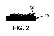
図2は、粗化後の光学表面の詳細図を示す。前記表面は、多数の不規則性12を含み、且つ従って大きい粗度を有する。
FIG. 2 shows a detailed view of the optical surface after roughening. The surface contains a large number of
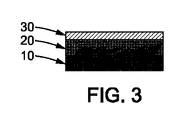
図3は、本発明による光学装置を製造する方法が使用された場合の、感圧接着剤層20及び熱可塑性薄膜30がその上にラミネートされている光学物品10の光学表面の詳細図を示す。感圧接着剤材料が表面の不規則性の周りで流動することができ、且つほとんど空洞を伴うことなく、更にはまったく空洞を伴うことなく連続的な媒体を提供し得ることを観察することができる。本発明者らは、光学装置がこのような構成を提示する場合、良好な光学特性が得られることを実証した。
FIG. 3 shows a detailed view of the optical surface of the
前記構成を得ることができる条件を判定するために、本発明者らは、複数の実験を実行した。 In order to determine the conditions under which the configuration can be obtained, the present inventors performed a plurality of experiments.
前記実験は、メガネレンズを使用して実行された。 The experiment was performed using a spectacle lens.
メガネレンズの透明性は、このようなレンズの適切な品質指数である。 The transparency of an eyeglass lens is a suitable quality index for such a lens.
光学コンポーネントは、そのコンポーネントを通じた画像の観察が、大きいコントラストの損失を伴うことなく知覚される場合に透明と見なされる。換言すれば、画像と画像の観察者との間の透明な光学コンポーネントの介在が画像の品質を大幅に低減しない。この透明という用語の定義は、本発明の意味では、本説明でそのように見なされているすべての物体に対して適用可能である。特定の場合、この定義は、光学物品が約1未満のヘイズ(haze)を有する場合に満たされたものと見なされる。 An optical component is considered transparent if image viewing through the component is perceived without significant contrast loss. In other words, the intervention of a transparent optical component between the image and the viewer of the image does not significantly reduce the image quality. This definition of the term transparent is applicable in the sense of the present invention to all objects so considered in this description. In certain cases, this definition is considered to be met when the optical article has a haze of less than about 1.
更に、ヘイズの値とは無関係に、光学装置は十分な光学品質を有する必要がある。 Furthermore, the optical device needs to have sufficient optical quality regardless of the haze value.
サンプルの光学品質の特徴を判定するために1つの方法を使用した。前記方法は、透過法であり、且つサンプルの光学品質は、訓練を受けた観察者により所定のプロトコルに従って計測される。 One method was used to determine the optical quality characteristics of the samples. The method is a transmission method and the optical quality of the sample is measured according to a predetermined protocol by a trained observer.
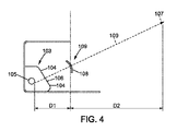
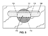
図4及び図5は、第1光学品質装置と、透明なサンプルの光学品質を判定するためのこの装置の使用法とを示す。前記装置は、不透明な壁104を有すると共に細長い光源105を含むボックス103を含む。前壁は、光源に対して平行に配置された細長いスリット106を含む。光源は、スリットに対向すると共に方向100に沿って観察している観察者107によって観察されないように、スリットからシフトされている。例えば、レンズ108などの計測対象のサンプルは、スリット106に対向するように、且つその光軸が方向100に対して平行になるように観察ゾーン109内に配置される。光源とサンプルとの間の距離D1は200mmである。サンプルと観察者の眼との間の距離D2は500mmである。周辺光は、60〜130ルクスでチューニングされる。主に光源105に起因する観察ゾーン109内の光は、600〜1200ルクスでチューニングされる。訓練を受けた観察者は、それぞれの眼ごとに10/10の視力を有するように選択される。観察者の観察位置では、観察者は、図5に従ってレンズを観察する。観察者は、例えば、レンズ108の表面の約3分の1である検査ゾーン110を観察することができる。検査ゾーン110は、レンズ108を通じて観察される光源105のエッジ111により、且つレンズ108を通じて観察されるスリット106のエッジ112により境界が画定される。レンズは、そのすべての表面が検査ゾーン110内で連続的に出現するように平行移動される。訓練を受けた観察者は、判定された期間にレンズ表面を観察し、且つ自身が、例えば、表面の異質性や引っ掻き傷などの光学的な欠陥を観察することができた場合に通知する。
4 and 5 show a first optical quality device and how to use this device to determine the optical quality of a transparent sample. The apparatus includes a
訓練を受けた観察者は、まず、昼光でサンプルを観察し、且つ次いで第1光学品質装置を使用し、且つ最後に第2光学品質装置を使用する。観察者は、1つ又は複数の光学的な欠陥が観察された場合、自身の観察を停止する。 A trained observer first observes the sample in daylight, then uses the first optical quality device, and finally uses the second optical quality device. The observer stops his / her observation when one or more optical defects are observed.
以下のプロトコルに従って、マークが付与される。
・5秒以下の期間に光学品質装置によってサンプルを観察した後、1つ(又はいくつか)の光学的欠陥が観察された場合、マーク=2である。欠陥の例は、歪円、ヘイズ円、引っ掻き傷である。
・5秒超且つ20秒以下である期間に品質装置によってサンプルを観察した後、1つ(又はいくつか)の光学的欠陥が観察された場合、マーク=1である。欠陥の例は、歪円、ヘイズ円、引っ掻き傷である。
・光学品質装置によってサンプルを観察した後、光学的欠陥が観察されない場合、マーク=0である。
マーク=1という結果は、受け入れ可能な結果として見なされ、マーク=0という結果は、良好な結果として見なされる。マーク=0とマーク=1との両方を有する結果を有するサンプルは、満足できる光学的品質を有するものとして見なされる。
Marks are assigned according to the following protocol.
• Mark = 1 if one (or several) optical defects are observed after observing the sample with the quality device in a period that is greater than 5 seconds and less than 20 seconds. Examples of defects are strain circles, haze circles, and scratches.
If the optical defect is not observed after observing the sample with an optical quality device, then mark = 0.
A result of mark = 1 is considered an acceptable result, and a result of mark = 0 is considered a good result. Samples with results that have both mark = 0 and mark = 1 are considered to have satisfactory optical quality.
受け入れ表面上で複数の粗度を得るように、異なる基材材料の137個のレンズサンプルを調製し、次いで0.00D〜−2.00Dで変化する光強度の137個のレンズ光学装置を提供するように、感圧接着剤層及び熱可塑性薄膜を前記受け入れ表面上にラミネートした。結果的に得られたレンズ光学装置の光学品質を上述のプロトコルに従って計測した。 Prepare 137 lens samples of different substrate materials to obtain multiple roughness on the receiving surface, then provide 137 lens optics with light intensity varying from 0.00D to -2.00D As such, a pressure sensitive adhesive layer and a thermoplastic thin film were laminated onto the receiving surface. The optical quality of the resulting lens optical device was measured according to the protocol described above.
これらの実施形態では、感圧接着剤層は、その商品名が3M(商標)Optically Clear Adhesive 8146−Xである感圧薄膜接着剤の一部分として提供され、感圧薄膜接着剤は、感圧接着剤層と、剥離可能な保護熱可塑性薄膜とを含み、感圧接着剤層は、保護熱可塑性薄膜上に存在するアクリルポリマーであり、感圧接着剤層が光学装置の受け入れ表面上に配置され、且つ保護熱可塑性薄膜が除去される。次いで、光学装置の熱可塑性薄膜が感圧接着剤上に適用される。光学装置の熱可塑性薄膜は、SZ80という品名でFuji Companyによって市販されているセルローストリアセテート(TAC)薄膜である。 In these embodiments, the pressure sensitive adhesive layer is provided as part of a pressure sensitive thin film adhesive whose trade name is 3M ™ Optically Clear Adhesive 8146-X, wherein the pressure sensitive thin film adhesive is a pressure sensitive adhesive. A pressure sensitive adhesive layer is an acrylic polymer present on the protective thermoplastic thin film, and the pressure sensitive adhesive layer is disposed on the receiving surface of the optical device. And the protective thermoplastic film is removed. The thermoplastic thin film of the optical device is then applied over the pressure sensitive adhesive. The thermoplastic thin film of the optical device is a cellulose triacetate (TAC) thin film marketed by Fuji Company under the name SZ80.
受け入れ表面の粗度は、Taylor Hobson Companyによって市販されているForm TalySurf(FTS)スタイラス装置によって計測した。スタイラスは、2μmのダイヤモンドポイントを有し、一定の圧力を伴って、1mm/sの速度においてこのスタイラスを受け入れ表面上で移動させる。計測誤差は、+/−2nmであるものと推定される。 The roughness of the receiving surface was measured with a Form TailSurf (FTS) stylus apparatus marketed by Taylor Hobson Company. The stylus has a diamond point of 2 μm and moves the stylus on the receiving surface at a speed of 1 mm / s with a constant pressure. The measurement error is estimated to be +/− 2 nm.
データの分析は、使用される薄膜が同一のものに留まる場合、光学品質に大きい影響を及ぼす唯一のパラメータが受け入れ表面の粗度であることを明らかにした。粗度がレンズサンプル間で類似している場合、レンズ材料の屈折率の変動は、光学品質に対して大きい影響を及ぼさない。 Analysis of the data revealed that if the thin film used remains the same, the only parameter that has a large effect on optical quality is the roughness of the receiving surface. If the roughness is similar between lens samples, the variation in the refractive index of the lens material does not have a significant effect on the optical quality.
感圧接着剤層及び熱可塑性薄膜の同時ラミネーションは、本発明の教示に従って実施された場合にサンプルの良好な品質を得るのに適することが実証された。 Simultaneous lamination of the pressure sensitive adhesive layer and the thermoplastic film has been demonstrated to be suitable for obtaining good sample quality when performed in accordance with the teachings of the present invention.
感圧接着剤層の厚さが20μm以上且つ250μm以下である場合、且つ更に好ましくは25μm以上且つ/又は75μm以下である場合に優れた結果が得られることが実証された。 It has been demonstrated that excellent results are obtained when the thickness of the pressure sensitive adhesive layer is 20 μm or more and 250 μm or less, and more preferably 25 μm or more and / or 75 μm or less.
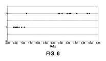
図6は、サンプルの計測されたプロファイル粗度二乗平均平方根勾配Rdqに応じたレンズ光学製品の計測された光学品質の変動を示す。(縦軸における)計測された光学品質は、上述のマーク番号付けに従って示されている。受け入れ表面が1.2°以下のプロファイル粗度二乗平均平方根勾配Rdqを有する場合、受け入れ可能な結果(マーク=1)が得られ、且つRdqが1.2°超である場合、結果が受け入れ不能である(マーク=2)ことを明瞭に理解することができる。 FIG. 6 shows the measured optical quality variation of the lens optical product as a function of the measured profile roughness root mean square slope R dq of the sample. The measured optical quality (in the vertical axis) is shown according to the mark numbering described above. If the receiving surface has a profile roughness root mean square slope R dq of 1.2 ° or less, obtained acceptable results (mark = 1), and when R dq is 1.2 ° greater, the result is It can be clearly understood that it is unacceptable (mark = 2).
従って、本発明者らは、感圧接着剤層及び熱可塑性薄膜がその上に直接ラミネートされる、前記特徴に応じた受け入れ表面を有する光学物品を含む光学装置を製造する場合に、優れた光学品質を実現することができる粗度特徴の範囲を選択した。 Accordingly, the inventors have found that when producing an optical device comprising an optical article having a receiving surface according to the above characteristics, a pressure sensitive adhesive layer and a thermoplastic thin film are directly laminated thereon. The range of roughness features that can realize the quality was selected.
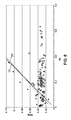
図7及び図8は、上述のように製造された光学装置の計測された光学品質に対する受け入れ表面の粗度特徴の影響を示す。これらの図のグラフでは、算術平均プロファイル粗度Raが横座標に示され、且つRSMと呼称されるピーク間の平均間隔が縦座標に示されている。 7 and 8 illustrate the effect of the roughness characteristics of the receiving surface on the measured optical quality of the optical device manufactured as described above. In the graphs of these figures, the arithmetic mean profile roughness Ra is shown on the abscissa, and the average spacing between peaks called RSM is shown on the ordinate.
実験データは、図7及び図8の(算術平均プロファイル粗度及びピーク間の平均間隔の)軸に従ってプロットされており、且つ図7と図8との間で変化しているのは情報の提示のみである。 The experimental data is plotted according to the axes of FIG. 7 and FIG. 8 (arithmetic mean profile roughness and average interval between peaks), and it is the presentation of information that varies between FIG. 7 and FIG. Only.
図7では、データは、3つの別個の標識を使用して示されており、この場合、
・エッジ上の黒色正方形は、良好な計測光学品質(マーク=0)を有するサンプルを示し、
・円形は、受け入れ可能な計測光学品質(マーク=1)を有するサンプルを示し、
・灰色の三角形は、受け入れ不能な計測光学品質(マーク=2)を有するサンプルを示す。
In FIG. 7, the data is shown using three separate indicators, where
The black square on the edge indicates a sample with good measurement optical quality (mark = 0)
• A circle indicates a sample with acceptable measurement optical quality (mark = 1)
• Gray triangles indicate samples with unacceptable metrology optical quality (mark = 2).
本発明者らは、算術平均プロファイル粗度とピーク間の平均間隔との間において、満足できる光学品質の取得を許容する受け入れ表面の粗度特徴の選択を許容する関係が存在することを発見した。 The inventors have discovered that there is a relationship between the arithmetic average profile roughness and the average spacing between peaks that allows the selection of roughness features on the receiving surface that allow obtaining satisfactory optical quality. .
以下の式
RSM≧min(0.64×Ra;0.58×Ra+0.007)
の要件が満たされるサンプルは、満足できる光学品質を有するサンプルであることが実証された。
The following formula RSM ≧ min (0.64 × Ra; 0.58 × Ra + 0.007)
It has been demonstrated that samples satisfying this requirement are samples with satisfactory optical quality.
図7では、
・直線の点線D1は、以下の式:
RSM=0.58×Ra+0.007
に対応し、
・直線の実線D2は、以下の式:
RSM=0.64×Ra
に対応する。
In FIG.
The straight dotted line D1 is the following formula:
RSM = 0.58 × Ra + 0.007
Corresponding to
-The solid line D2 is the following formula:
RSM = 0.64 × Ra
Corresponding to
図8にはいくつかのデータがプロットされ、且つ同一のラインD1及びD2が報告されており、このデータは、5つの別個の標識を使用して示されており、この場合、
・正方形は、光学物品が1.67の屈折率を有するサンプルを示し、
・明るい三角形は、光学物品が1.59の屈折率を有するサンプルを示し、
・星形は、光学物品が1.53の屈折率を有するサンプルを示し、
・灰色の円形は、光学物品が1.56の屈折率を有するサンプルを示し、
・黒色の三角形は、光学物品が1.49の屈折率を有するサンプルを示す。
In FIG. 8, several data are plotted and the same lines D1 and D2 are reported, and this data is shown using five separate labels, where:
The squares indicate samples where the optical article has a refractive index of 1.67;
A bright triangle indicates a sample in which the optical article has a refractive index of 1.59;
The star shape indicates a sample in which the optical article has a refractive index of 1.53;
The gray circle indicates a sample in which the optical article has a refractive index of 1.56;
The black triangle indicates a sample where the optical article has a refractive index of 1.49.
これらのデータは、光学物品の特性が、算術平均プロファイル粗度とピーク間の平均間隔との間において、満足できる光学品質の取得を許容する受け入れ表面の粗度特性の選択を許容する関係を判定する際に役割を果たしていないことを明瞭に実証している。 These data determine the relationship in which the properties of the optical article allow the selection of the roughness characteristics of the receiving surface that allow satisfactory optical quality acquisition between the arithmetic average profile roughness and the average spacing between peaks. It clearly demonstrates that it does not play a role.
本発明の選択された粗度特徴により、本発明者らは、驚くべきことに、光学装置が、凸状及び/又は凹状の受け入れ表面と、受け入れ表面上に直接ラミネートされた感圧接着剤層及び熱可塑性薄膜とを含む光学物品を含む場合、良好な、更には優れた光学品質を有する光学装置を取得することが可能であり、この場合、前記受け入れ表面の粗度は、通常の研磨された受け入れ表面の粗度を大幅に上回っており、この場合、Rdq<0.2°又はRa<0.1μmであることを実証した。 Due to the selected roughness characteristics of the present invention, the inventors have surprisingly found that the optical device has a convex and / or concave receiving surface and a pressure sensitive adhesive layer laminated directly onto the receiving surface. And an optical article comprising a thermoplastic thin film, it is possible to obtain an optical device with good and even good optical quality, in which case the roughness of the receiving surface is normal polished. The roughness of the receiving surface was significantly higher, in which case it was demonstrated that Rdq <0.2 ° or Ra <0.1 μm.
従って、その受け入れ表面が、粗化ステップ、微細化ステップ、及び研磨ステップの2つ以下によって表面処理されている光学物品を使用することができる。 Thus, an optical article can be used whose receiving surface has been surface treated by no more than two of a roughening step, a finening step, and a polishing step.
その受け入れ表面が粗化ステップのみによって表面処理されている光学物品を使用することもできる。 It is also possible to use optical articles whose receiving surfaces are surface treated only by a roughening step.
従って、受け入れ表面を表面処理する際に機械加工ステップを節約するために、且つ本発明による光学装置の良好な、更には優れた光学品質を依然として得るために、本発明による光学物品を使用することができる。 Therefore, to use the optical article according to the invention in order to save machining steps when surface-treating the receiving surface and still obtain good and even better optical quality of the optical device according to the invention Can do.
従って、本発明の光学装置を製造する方法は、非常に高度な費用効率を有することができる。 Thus, the method of manufacturing the optical device of the present invention can be very cost effective.
前記方法は、上述のように多数のサブステップを伴って実施することができる。 The method can be implemented with a number of sub-steps as described above.
それらのうち、制御ステップ及び意思決定ステップによって後続される、互いに対向する凸状及び凹状の光学表面を含む供給された光学物品を提供する予備ステップを実施することが可能であり、この場合、
・制御ステップは、受け入れ表面となることを意図される供給された光学物品の表面の粗度を判定するステップを含み、
・意思決定ステップは、
i.前記光学表面の予め判定された粗度を、選択された粗度特徴を有する光学物品の受け入れ表面の1つと比較するサブステップと、
ii.選択された粗度特徴に対応する粗度要件が満たされる場合、供給された光学物品を製造方法の提供ステップに提供し、且つ選択された粗度特徴に対応する粗度要件が満たされない場合、供給された光学物品を補完ステップに提供するサブステップと
を含む。
Among them, it is possible to carry out a preliminary step of providing a supplied optical article comprising convex and concave optical surfaces facing each other, followed by a control step and a decision-making step, where
The controlling step comprises determining the roughness of the surface of the supplied optical article intended to be the receiving surface;
・ The decision-making step is
i. Comparing the predetermined roughness of the optical surface with one of the receiving surfaces of an optical article having a selected roughness feature;
ii. If the roughness requirement corresponding to the selected roughness feature is met, the supplied optical article is provided to the providing step of the manufacturing method, and if the roughness requirement corresponding to the selected roughness feature is not met, Providing the supplied optical article to the complementary step.
受け入れ表面となることを意図される表面の粗度を判定するステップは、例えば、前記表面の粗度を計測するステップと、前記表面の事前の製造データに基づいて前記表面の粗度を推定するステップと、前記表面を既知の粗度の表面と比較するステップとからなるリスト内で選択される方法に従って実施することができる。 The step of determining the roughness of the surface intended to be the receiving surface includes, for example, measuring the roughness of the surface and estimating the roughness of the surface based on prior manufacturing data of the surface. It can be performed according to a method selected in a list consisting of a step and comparing the surface with a surface of known roughness.
補完ステップは、上述の微細化又は研磨ステップに類似したステップであってもよい。 The complementing step may be a step similar to the above-described miniaturization or polishing step.
Claims (15)
RSM≧min(0.64×Ra;0.58×Ra+0.007)
による、RSMと呼称されるピーク間の平均間隔を有し、
例えば、RSM≧0.64×Raであり、又は
例えば、RSM≧0.58×Ra+0.007である、請求項1又は2に記載の光学物品。 The receiving surface has the following formula:
RSM ≧ min (0.64 × R a ; 0.58 × R a +0.007)
With an average spacing between peaks called RSM,
The optical article according to claim 1, wherein, for example, RSM ≧ 0.64 × R a or, for example, RSM ≧ 0.58 × R a +0.007.
・請求項1〜3のいずれか一項に記載の光学物品を提供するステップと、
・感圧接着剤層及び熱可塑性薄膜を提供するステップと、
・前記感圧接着剤が前記受け入れ表面上に接着し、及び前記熱可塑性薄膜が前記感圧接着剤上に配置されるように、前記感圧接着剤層及び前記熱可塑性薄膜を前記光学物品の受け入れ表面上に直接ラミネートするステップと
を含む方法。 A method of manufacturing an optical device comprising:
Providing the optical article according to any one of claims 1 to 3;
Providing a pressure sensitive adhesive layer and a thermoplastic film;
The pressure sensitive adhesive layer and the thermoplastic thin film are bonded to the optical article such that the pressure sensitive adhesive adheres to the receiving surface and the thermoplastic thin film is disposed on the pressure sensitive adhesive; Laminating directly on the receiving surface.
・前記制御ステップは、受け入れ表面となることを意図される前記供給された光学物品の表面の粗度を判定するステップを含み、
・前記意思決定ステップは、
i.前記光学表面の前記予め判定された粗度を、請求項1〜3のいずれか一項に記載の光学物品の受け入れ表面の1つと比較するサブステップと、
ii.請求項1〜3のいずれか一項に記載の粗度要件が満たされる場合、前記供給された光学物品を請求項6に記載の製造方法の前記提供ステップに提供し、且つ請求項1〜3のいずれか一項に記載の粗度要件が満たされない場合、前記供給された光学物品を補完ステップに提供するサブステップと
を含む、請求項6〜12のいずれか一項に記載の製造方法。 Providing a provisioned optical article comprising convex and concave optical surfaces facing each other, followed by a control step and a decision-making step,
The controlling step comprises determining the roughness of the surface of the supplied optical article intended to be a receiving surface;
The decision making step is
i. Comparing the pre-determined roughness of the optical surface with one of the receiving surfaces of the optical article according to any one of claims 1 to 3;
ii. When the roughness requirement according to any one of claims 1 to 3 is satisfied, the supplied optical article is provided to the providing step of the manufacturing method according to claim 6, and claims 1 to 3 are provided. The manufacturing method according to any one of claims 6 to 12, further comprising a sub-step of providing the supplied optical article to a supplementing step when the roughness requirement according to any one of the above is not satisfied.
Applications Claiming Priority (3)
| Application Number | Priority Date | Filing Date | Title |
|---|---|---|---|
| EP15306531.3A EP3150364B1 (en) | 2015-09-29 | 2015-09-29 | Method for manufacturing an optical device |
| EP15306531.3 | 2015-09-29 | ||
| PCT/EP2016/072956 WO2017055265A1 (en) | 2015-09-29 | 2016-09-27 | Optical article provided in a form suitable for direct lamination; method for manufacturing an optical device |
Publications (2)
| Publication Number | Publication Date |
|---|---|
| JP2018537726A true JP2018537726A (en) | 2018-12-20 |
| JP6943863B2 JP6943863B2 (en) | 2021-10-06 |
Family
ID=54251465
Family Applications (1)
| Application Number | Title | Priority Date | Filing Date |
|---|---|---|---|
| JP2018535241A Active JP6943863B2 (en) | 2015-09-29 | 2016-09-27 | A method of manufacturing optical articles and optics provided in a form suitable for direct lamination. |
Country Status (7)
| Country | Link |
|---|---|
| US (2) | US11099299B2 (en) |
| EP (2) | EP3150364B1 (en) |
| JP (1) | JP6943863B2 (en) |
| KR (1) | KR102530249B1 (en) |
| CN (1) | CN108025517B (en) |
| BR (1) | BR112018006123B1 (en) |
| WO (1) | WO2017055265A1 (en) |
Families Citing this family (3)
| Publication number | Priority date | Publication date | Assignee | Title |
|---|---|---|---|---|
| EP3587093A1 (en) * | 2018-06-28 | 2020-01-01 | Essilor International | Device and method for forming a functional film intended to be laminated on an optical article |
| EP3763517A1 (en) * | 2019-07-09 | 2021-01-13 | Essilor International | Method for manufacturing a photochromic optical article |
| US12429714B2 (en) | 2019-11-26 | 2025-09-30 | Oakley, Inc. | High transmittance eyewear with chroma enhancement |
Citations (10)
| Publication number | Priority date | Publication date | Assignee | Title |
|---|---|---|---|---|
| JPS603601A (en) * | 1983-06-22 | 1985-01-10 | Olympus Optical Co Ltd | Joined optical element |
| JPS62196613A (en) * | 1986-02-25 | 1987-08-31 | Hitachi Ltd | aspherical lens |
| JPH035702A (en) * | 1989-06-01 | 1991-01-11 | Canon Inc | Cemented lens or the like and its manufacture |
| US20030137634A1 (en) * | 2000-01-24 | 2003-07-24 | Dungar Christopher Mark | Method and kit for making ophthalmic lenses |
| JP2007226241A (en) * | 2006-02-23 | 2007-09-06 | Essilor Internatl (Co Generale D'optique) | Method for producing polarizing optical element |
| JP2008040497A (en) * | 2006-08-07 | 2008-02-21 | Stephen M Dillon | Uniform diffuse omnidirectional reflective lens |
| JP2010101918A (en) * | 2008-09-26 | 2010-05-06 | Toshiba Corp | Spectacles |
| JP2010536060A (en) * | 2007-08-08 | 2010-11-25 | エシロール アテルナジオナール カンパニー ジェネラーレ デ オプティック | Method of providing a coated or uncoated film on a lens substrate |
| JP2012008524A (en) * | 2010-02-26 | 2012-01-12 | Canon Inc | Optical member, polyimide, and method for manufacturing the same |
| JP2014048242A (en) * | 2012-09-03 | 2014-03-17 | Hoya Corp | Ophthalmic lens manufacturing method and ophthalmic lens evaluation method |
Family Cites Families (8)
| Publication number | Priority date | Publication date | Assignee | Title |
|---|---|---|---|---|
| JP3334911B2 (en) * | 1992-07-31 | 2002-10-15 | キヤノン株式会社 | Pattern formation method |
| KR100301948B1 (en) * | 1999-05-11 | 2001-09-22 | 윤덕용 | Apparatus and method of polishing aspherical surface lens |
| FR2883984B1 (en) | 2005-04-04 | 2007-06-22 | Essilor Int | APPARATUS FOR CONFORMING PLANAR FILM TO AN OPTICAL LENS, METHODS OF FUNCTIONALIZING AN OPTICAL LENS USING THE SAME, AND LENS OBTAINED THEREBY |
| FR2897693B1 (en) * | 2006-02-23 | 2008-11-21 | Essilor Int | POLARIZING OPTICAL ELEMENT COMPRISING A POLARIZER FILM AND METHOD OF FARBINATING SUCH A ELEMENT |
| DE102006060141A1 (en) * | 2006-12-18 | 2008-06-26 | Docter Optics Gmbh | Headlight lens for a motor vehicle headlight |
| KR20100020906A (en) * | 2008-08-13 | 2010-02-23 | 소니 가부시끼가이샤 | Optical film and manufacturing method therefor, antiglare film, optical layer-attached polarizer, and display apparatus |
| FR2979713B1 (en) * | 2011-09-06 | 2013-09-20 | Bnl Eurolens | POLARISANT TINTED OPTICAL ELEMENT AND METHOD FOR MANUFACTURING THE SAME |
| PT2724815E (en) | 2012-10-29 | 2014-08-28 | Essilor Int | Method for machining a surface of an optical lens |
-
2015
- 2015-09-29 EP EP15306531.3A patent/EP3150364B1/en active Active
-
2016
- 2016-09-27 EP EP16775174.2A patent/EP3356127B1/en active Active
- 2016-09-27 US US15/764,424 patent/US11099299B2/en active Active
- 2016-09-27 WO PCT/EP2016/072956 patent/WO2017055265A1/en not_active Ceased
- 2016-09-27 KR KR1020187011800A patent/KR102530249B1/en active Active
- 2016-09-27 CN CN201680056447.8A patent/CN108025517B/en active Active
- 2016-09-27 BR BR112018006123-9A patent/BR112018006123B1/en active IP Right Grant
- 2016-09-27 JP JP2018535241A patent/JP6943863B2/en active Active
-
2021
- 2021-06-30 US US17/363,210 patent/US20210325568A1/en not_active Abandoned
Patent Citations (10)
| Publication number | Priority date | Publication date | Assignee | Title |
|---|---|---|---|---|
| JPS603601A (en) * | 1983-06-22 | 1985-01-10 | Olympus Optical Co Ltd | Joined optical element |
| JPS62196613A (en) * | 1986-02-25 | 1987-08-31 | Hitachi Ltd | aspherical lens |
| JPH035702A (en) * | 1989-06-01 | 1991-01-11 | Canon Inc | Cemented lens or the like and its manufacture |
| US20030137634A1 (en) * | 2000-01-24 | 2003-07-24 | Dungar Christopher Mark | Method and kit for making ophthalmic lenses |
| JP2007226241A (en) * | 2006-02-23 | 2007-09-06 | Essilor Internatl (Co Generale D'optique) | Method for producing polarizing optical element |
| JP2008040497A (en) * | 2006-08-07 | 2008-02-21 | Stephen M Dillon | Uniform diffuse omnidirectional reflective lens |
| JP2010536060A (en) * | 2007-08-08 | 2010-11-25 | エシロール アテルナジオナール カンパニー ジェネラーレ デ オプティック | Method of providing a coated or uncoated film on a lens substrate |
| JP2010101918A (en) * | 2008-09-26 | 2010-05-06 | Toshiba Corp | Spectacles |
| JP2012008524A (en) * | 2010-02-26 | 2012-01-12 | Canon Inc | Optical member, polyimide, and method for manufacturing the same |
| JP2014048242A (en) * | 2012-09-03 | 2014-03-17 | Hoya Corp | Ophthalmic lens manufacturing method and ophthalmic lens evaluation method |
Also Published As
| Publication number | Publication date |
|---|---|
| EP3356127A1 (en) | 2018-08-08 |
| BR112018006123B1 (en) | 2022-04-05 |
| EP3150364B1 (en) | 2018-11-14 |
| EP3150364A1 (en) | 2017-04-05 |
| KR102530249B1 (en) | 2023-05-09 |
| KR20180061277A (en) | 2018-06-07 |
| US20180284325A1 (en) | 2018-10-04 |
| WO2017055265A1 (en) | 2017-04-06 |
| BR112018006123A2 (en) | 2018-10-23 |
| CN108025517B (en) | 2020-11-24 |
| US11099299B2 (en) | 2021-08-24 |
| JP6943863B2 (en) | 2021-10-06 |
| US20210325568A1 (en) | 2021-10-21 |
| CN108025517A (en) | 2018-05-11 |
| EP3356127B1 (en) | 2020-05-06 |
Similar Documents
| Publication | Publication Date | Title |
|---|---|---|
| US20210325568A1 (en) | Optical article provided in a form suitable for direct lamination; method for manufacturing an optical device | |
| US9304330B2 (en) | Experiential optical device | |
| CN207752263U (en) | Laminated Mirror Lenses and Eyewear | |
| US20150331259A1 (en) | Film Laminated Ophthalmic Lenses with Improved Wheel Edging Performance | |
| US20190324289A1 (en) | Spectacle lens comprising at least one ultrathin lens and process for production thereof | |
| CN109130260A (en) | Manufacture the method and polarization optics product of polarization optics product | |
| CN102985220A (en) | Method for trimming an ophthalmic eyeglass lens comprising a coating film | |
| JP2016509250A (en) | Edgeable ophthalmic lens comprising a hydrophobic bilayer and a temporary metal fluoride layer | |
| JP5511287B2 (en) | Manufacturing method of plastic lens | |
| JP6691920B2 (en) | Optical element | |
| JP2019518230A (en) | Functionalized laminated optics with improved edging resistance | |
| US10274656B2 (en) | Optical device with a functionalised coating and method for such optical device | |
| US11106057B2 (en) | Temporary polar patches | |
| WO2023110887A1 (en) | Method for thermoforming a film by thermal shrinkage and lamination thereof on an optical article | |
| CN120091909A (en) | Release liner for protecting optical sheets | |
| JP2023031185A (en) | Seal for spectacle lens | |
| JP2012215640A (en) | Spectacle lens manufacturing method | |
| GB2494936A (en) | Lens engraved with image logo or text |
Legal Events
| Date | Code | Title | Description |
|---|---|---|---|
| A621 | Written request for application examination |
Free format text: JAPANESE INTERMEDIATE CODE: A621 Effective date: 20190927 |
|
| A977 | Report on retrieval |
Free format text: JAPANESE INTERMEDIATE CODE: A971007 Effective date: 20200722 |
|
| A131 | Notification of reasons for refusal |
Free format text: JAPANESE INTERMEDIATE CODE: A131 Effective date: 20200811 |
|
| A521 | Request for written amendment filed |
Free format text: JAPANESE INTERMEDIATE CODE: A523 Effective date: 20201106 |
|
| A131 | Notification of reasons for refusal |
Free format text: JAPANESE INTERMEDIATE CODE: A131 Effective date: 20210419 |
|
| A521 | Request for written amendment filed |
Free format text: JAPANESE INTERMEDIATE CODE: A523 Effective date: 20210716 |
|
| TRDD | Decision of grant or rejection written | ||
| A01 | Written decision to grant a patent or to grant a registration (utility model) |
Free format text: JAPANESE INTERMEDIATE CODE: A01 Effective date: 20210816 |
|
| A61 | First payment of annual fees (during grant procedure) |
Free format text: JAPANESE INTERMEDIATE CODE: A61 Effective date: 20210909 |
|
| R150 | Certificate of patent or registration of utility model |
Ref document number: 6943863 Country of ref document: JP Free format text: JAPANESE INTERMEDIATE CODE: R150 |
|
| R250 | Receipt of annual fees |
Free format text: JAPANESE INTERMEDIATE CODE: R250 |
|
| R250 | Receipt of annual fees |
Free format text: JAPANESE INTERMEDIATE CODE: R250 |