JP2018530098A - Refresh timer synchronization between memory controller and memory - Google Patents
Refresh timer synchronization between memory controller and memory Download PDFInfo
- Publication number
- JP2018530098A JP2018530098A JP2018516132A JP2018516132A JP2018530098A JP 2018530098 A JP2018530098 A JP 2018530098A JP 2018516132 A JP2018516132 A JP 2018516132A JP 2018516132 A JP2018516132 A JP 2018516132A JP 2018530098 A JP2018530098 A JP 2018530098A
- Authority
- JP
- Japan
- Prior art keywords
- refresh
- dram
- memory controller
- self
- mode
- Prior art date
- Legal status (The legal status is an assumption and is not a legal conclusion. Google has not performed a legal analysis and makes no representation as to the accuracy of the status listed.)
- Pending
Links
Images


Classifications
-
- G—PHYSICS
- G11—INFORMATION STORAGE
- G11C—STATIC STORES
- G11C11/00—Digital stores characterised by the use of particular electric or magnetic storage elements; Storage elements therefor
- G11C11/21—Digital stores characterised by the use of particular electric or magnetic storage elements; Storage elements therefor using electric elements
- G11C11/34—Digital stores characterised by the use of particular electric or magnetic storage elements; Storage elements therefor using electric elements using semiconductor devices
- G11C11/40—Digital stores characterised by the use of particular electric or magnetic storage elements; Storage elements therefor using electric elements using semiconductor devices using transistors
- G11C11/401—Digital stores characterised by the use of particular electric or magnetic storage elements; Storage elements therefor using electric elements using semiconductor devices using transistors forming cells needing refreshing or charge regeneration, i.e. dynamic cells
- G11C11/406—Management or control of the refreshing or charge-regeneration cycles
- G11C11/40615—Internal triggering or timing of refresh, e.g. hidden refresh, self refresh, pseudo-SRAMs
-
- G—PHYSICS
- G06—COMPUTING; CALCULATING OR COUNTING
- G06F—ELECTRIC DIGITAL DATA PROCESSING
- G06F13/00—Interconnection of, or transfer of information or other signals between, memories, input/output devices or central processing units
- G06F13/14—Handling requests for interconnection or transfer
- G06F13/16—Handling requests for interconnection or transfer for access to memory bus
- G06F13/1605—Handling requests for interconnection or transfer for access to memory bus based on arbitration
- G06F13/161—Handling requests for interconnection or transfer for access to memory bus based on arbitration with latency improvement
- G06F13/1636—Handling requests for interconnection or transfer for access to memory bus based on arbitration with latency improvement using refresh
-
- G—PHYSICS
- G11—INFORMATION STORAGE
- G11C—STATIC STORES
- G11C11/00—Digital stores characterised by the use of particular electric or magnetic storage elements; Storage elements therefor
- G11C11/21—Digital stores characterised by the use of particular electric or magnetic storage elements; Storage elements therefor using electric elements
- G11C11/34—Digital stores characterised by the use of particular electric or magnetic storage elements; Storage elements therefor using electric elements using semiconductor devices
- G11C11/40—Digital stores characterised by the use of particular electric or magnetic storage elements; Storage elements therefor using electric elements using semiconductor devices using transistors
- G11C11/401—Digital stores characterised by the use of particular electric or magnetic storage elements; Storage elements therefor using electric elements using semiconductor devices using transistors forming cells needing refreshing or charge regeneration, i.e. dynamic cells
- G11C11/406—Management or control of the refreshing or charge-regeneration cycles
- G11C11/40611—External triggering or timing of internal or partially internal refresh operations, e.g. auto-refresh or CAS-before-RAS triggered refresh
-
- G—PHYSICS
- G11—INFORMATION STORAGE
- G11C—STATIC STORES
- G11C11/00—Digital stores characterised by the use of particular electric or magnetic storage elements; Storage elements therefor
- G11C11/21—Digital stores characterised by the use of particular electric or magnetic storage elements; Storage elements therefor using electric elements
- G11C11/34—Digital stores characterised by the use of particular electric or magnetic storage elements; Storage elements therefor using electric elements using semiconductor devices
- G11C11/40—Digital stores characterised by the use of particular electric or magnetic storage elements; Storage elements therefor using electric elements using semiconductor devices using transistors
- G11C11/401—Digital stores characterised by the use of particular electric or magnetic storage elements; Storage elements therefor using electric elements using semiconductor devices using transistors forming cells needing refreshing or charge regeneration, i.e. dynamic cells
- G11C11/406—Management or control of the refreshing or charge-regeneration cycles
- G11C11/40626—Temperature related aspects of refresh operations
-
- G—PHYSICS
- G11—INFORMATION STORAGE
- G11C—STATIC STORES
- G11C11/00—Digital stores characterised by the use of particular electric or magnetic storage elements; Storage elements therefor
- G11C11/21—Digital stores characterised by the use of particular electric or magnetic storage elements; Storage elements therefor using electric elements
- G11C11/34—Digital stores characterised by the use of particular electric or magnetic storage elements; Storage elements therefor using electric elements using semiconductor devices
- G11C11/40—Digital stores characterised by the use of particular electric or magnetic storage elements; Storage elements therefor using electric elements using semiconductor devices using transistors
- G11C11/401—Digital stores characterised by the use of particular electric or magnetic storage elements; Storage elements therefor using electric elements using semiconductor devices using transistors forming cells needing refreshing or charge regeneration, i.e. dynamic cells
- G11C11/4063—Auxiliary circuits, e.g. for addressing, decoding, driving, writing, sensing or timing
- G11C11/407—Auxiliary circuits, e.g. for addressing, decoding, driving, writing, sensing or timing for memory cells of the field-effect type
- G11C11/4076—Timing circuits
-
- G—PHYSICS
- G11—INFORMATION STORAGE
- G11C—STATIC STORES
- G11C11/00—Digital stores characterised by the use of particular electric or magnetic storage elements; Storage elements therefor
- G11C11/21—Digital stores characterised by the use of particular electric or magnetic storage elements; Storage elements therefor using electric elements
- G11C11/34—Digital stores characterised by the use of particular electric or magnetic storage elements; Storage elements therefor using electric elements using semiconductor devices
- G11C11/40—Digital stores characterised by the use of particular electric or magnetic storage elements; Storage elements therefor using electric elements using semiconductor devices using transistors
- G11C11/401—Digital stores characterised by the use of particular electric or magnetic storage elements; Storage elements therefor using electric elements using semiconductor devices using transistors forming cells needing refreshing or charge regeneration, i.e. dynamic cells
- G11C11/4063—Auxiliary circuits, e.g. for addressing, decoding, driving, writing, sensing or timing
- G11C11/407—Auxiliary circuits, e.g. for addressing, decoding, driving, writing, sensing or timing for memory cells of the field-effect type
- G11C11/408—Address circuits
- G11C11/4087—Address decoders, e.g. bit - or word line decoders; Multiple line decoders
-
- G—PHYSICS
- G11—INFORMATION STORAGE
- G11C—STATIC STORES
- G11C2211/00—Indexing scheme relating to digital stores characterized by the use of particular electric or magnetic storage elements; Storage elements therefor
- G11C2211/401—Indexing scheme relating to cells needing refreshing or charge regeneration, i.e. dynamic cells
- G11C2211/406—Refreshing of dynamic cells
- G11C2211/4067—Refresh in standby or low power modes
Landscapes
- Engineering & Computer Science (AREA)
- Microelectronics & Electronic Packaging (AREA)
- Computer Hardware Design (AREA)
- Theoretical Computer Science (AREA)
- Physics & Mathematics (AREA)
- General Engineering & Computer Science (AREA)
- General Physics & Mathematics (AREA)
- Dram (AREA)
Abstract
メモリコントローラは、DRAMがそのリフレッシュサイクルをセルフトリガするセルフリフレッシュ動作モードに移行する前に、最新のメモリコントローラによってトリガされたリフレッシュサイクルが発生した時の表示をDRAMに通信するように構成される。The memory controller is configured to communicate to the DRAM a display when a refresh cycle triggered by the latest memory controller occurs before the DRAM enters a self-refresh mode of operation that self-triggers its refresh cycle.
Description
関連出願の相互参照
本出願は、2015年10月1日に出願された米国仮出願第62/236,008号の利益を主張する、2016年8月24日に出願された米国特許出願第15/246,371号の優先権を主張するものであり、参照により本明細書に含まれる。
CROSS REFERENCE TO RELATED APPLICATIONS Claim of priority and are hereby incorporated by reference.
本出願は、メモリに関し、より詳細には、メモリコントローラと対応するメモリとの間のリフレッシュタイマ同期に関する。 This application relates to memory, and more particularly to refresh timer synchronization between a memory controller and a corresponding memory.
ダイナミックランダムアクセスメモリ(DRAM)は、各メモリセルがアクセストランジスタおよびコンデンサだけを必要とするため、比較的安価である。対照的に、スタティックランダムアクセスメモリ(SRAM)は、メモリセル当たり少なくとも6つのトランジスタを必要とし、したがってより高価である。したがって、スマートフォンのような多くの電子デバイスにおける大容量記憶装置にとって最適なメモリは、DRAMである。DRAMはかなり安価であるが、各メモリセルに使用される比較的小さいコンデンサは経時的に電荷を漏えいするので、その内容を定期的にリフレッシュする必要がある。DRAMのリフレッシュサイクルにおいては、メモリセルのコンデンサが適切に再充電され得るように、メモリセルの内容が読み出される。DRAMがそのリフレッシュスケジュールに従って定期的にリフレッシュすることは重要であり、そうしないとそのメモリ内容を失う可能性がある。 Dynamic random access memory (DRAM) is relatively inexpensive because each memory cell requires only an access transistor and a capacitor. In contrast, static random access memory (SRAM) requires at least six transistors per memory cell and is therefore more expensive. Therefore, the most suitable memory for mass storage devices in many electronic devices such as smartphones is DRAM. DRAM is fairly inexpensive, but the relatively small capacitors used in each memory cell will leak charge over time, so the contents need to be refreshed regularly. In the DRAM refresh cycle, the contents of the memory cells are read so that the capacitors of the memory cells can be properly recharged. It is important that the DRAM refresh periodically according to its refresh schedule, otherwise the memory contents may be lost.
必要なリフレッシュ間隔に従うリフレッシュ動作の実施は、ホストプロセッサと対応するDRAMとの間のインターフェースとして動作するメモリコントローラによって実行され得る。従来のデスクトップおよび関連するアプリケーションにおいては、メモリコントローラは、通常、DRAM集積回路を受け入れるメモリスロットに関連付けられる別個の集積回路に含まれる。そのようなスタンドアロンメモリコントローラは、ホストプロセッサとは独立して、通常の動作中は電力を供給されたままであり得る。しかし、スマートフォンなどの最新のモバイルデバイスアプリケーションにおいては、メモリコントローラはホストプロセッサとシステムオンチップ(SoC)に統合されている。消費者は彼らのデバイスを絶えず再充電したくはないので、SoCによる消費電力の削減はスマートフォン設計における主な目標である。したがって、モバイルデバイスSoCが、メモリコントローラが完全にまたは部分的のいずれかにパワーダウンされるスリープモードを実装することは従来通りである。しかし、SoC用の関連付けられるDRAM集積回路は、そのメモリ内容を保持し得るように、スリープモード中は電源を入れたままでなければならない。したがって、モバイルデバイスおよび関連デバイスにおけるDRAMのリフレッシュスケジューリングは、アクティブ動作モードの間はメモリコントローラによって制御され、アイドル動作モードまたはスリープ動作モードの間はDRAM自体によって制御される。2つのタイプのリフレッシュスケジューリング管理を区別するために、メモリコントローラによって管理されるリフレッシュスケジューリングは、動作の「リフレッシュモード」として示され得、DRAMによって制御されるリフレッシュスケジューリングは、動作の「セルフリフレッシュモード」として示され得る。 Implementation of the refresh operation according to the required refresh interval may be performed by a memory controller that acts as an interface between the host processor and the corresponding DRAM. In conventional desktop and related applications, the memory controller is typically included in a separate integrated circuit associated with a memory slot that accepts a DRAM integrated circuit. Such a stand-alone memory controller may remain powered during normal operation, independent of the host processor. However, in modern mobile device applications such as smartphones, the memory controller is integrated into the host processor and system on chip (SoC). Because consumers do not want to recharge their devices constantly, reducing power consumption with SoC is a major goal in smartphone design. Thus, it is conventional for the mobile device SoC to implement a sleep mode in which the memory controller is powered down either completely or partially. However, the associated DRAM integrated circuit for the SoC must remain powered during sleep mode so that its memory contents can be retained. Accordingly, DRAM refresh scheduling in mobile devices and associated devices is controlled by the memory controller during the active mode of operation and by the DRAM itself during the idle mode or sleep mode of operation. To distinguish between the two types of refresh scheduling management, the refresh scheduling managed by the memory controller may be denoted as the “refresh mode” of operation, and the refresh scheduling controlled by DRAM is the “self-refresh mode” of operation. Can be shown as
モバイルデバイスにおけるこのリフレッシュスケジューリングのこのスプリット制御により、SoCはスリープモードに入ることによって電力を節約することが可能になるが、それはリフレッシュサイクルの不要なトリガと関連付けられる。たとえば、リフレッシュ動作モードの間、リフレッシュスケジュールのタイミングはメモリコントローラによって管理されているので、DRAMはリフレッシュスケジュールのタイミングを追跡しない。したがって、DRAMは、セルフリフレッシュ動作モードの再開時にリフレッシュ動作をトリガする。しかし、メモリコントローラは、セルフリフレッシュモードへの移行時にDRAMによるリフレッシュ動作の自動トリガが不要となるように、セルフリフレッシュ動作モードへのハンドオフの前にリフレッシュ動作をトリガしたばかりである場合がある。同様に、メモリコントローラは、リフレッシュ動作モードの再開時およびセルフリフレッシュモードの終了時にリフレッシュ動作をトリガする。DRAMにおける最後のリフレッシュサイクルのタイミングに応じて、リフレッシュモードへの移行時にメモリコントローラによるリフレッシュ動作の自動トリガも不要であり得る。これらの不要なリフレッシュサイクルが、電力を不必要に消費する。さらに、リフレッシュサイクルが完了するまで、リードアクセスおよびライトアクセスのためにDRAMを使用できないため、メモリレイテンシが増加する。消費電力を最小限に抑えるためにスリープモードにより頻繁に入るように設計された最新のSoCにおいて、レイテンシと消費電力の増加というこの問題が深刻化している。 This split control of this refresh scheduling in the mobile device allows the SoC to save power by entering sleep mode, which is associated with an unnecessary trigger for the refresh cycle. For example, during the refresh mode of operation, the refresh schedule timing is managed by the memory controller, so the DRAM does not track the refresh schedule timing. Therefore, the DRAM triggers a refresh operation when the self-refresh operation mode is resumed. However, the memory controller may have just triggered the refresh operation before handing off to the self-refresh operation mode so that automatic triggering of the refresh operation by the DRAM is not required when shifting to the self-refresh mode. Similarly, the memory controller triggers a refresh operation when the refresh operation mode is resumed and when the self-refresh mode ends. Depending on the timing of the last refresh cycle in the DRAM, automatic triggering of the refresh operation by the memory controller may be unnecessary when the mode is changed to the refresh mode. These unnecessary refresh cycles consume power unnecessarily. Further, since the DRAM cannot be used for read access and write access until the refresh cycle is completed, the memory latency increases. In modern SoCs designed to enter more frequently in sleep mode to minimize power consumption, this problem of increased latency and power consumption is exacerbated.
したがって、メモリコントローラとメモリ自体との両方がリフレッシュスケジューリングを制御し得る、システムにおける改善されたリフレッシュスケジューリングが当分野において必要とされている。 Therefore, there is a need in the art for improved refresh scheduling in a system where both the memory controller and the memory itself can control refresh scheduling.
改善されたリフレッシュスケジューリングを提供するために、スリープ動作モードに入る前に、最新のメモリコントローラによってトリガされたリフレッシュサイクルがメモリコントローラによってトリガされた時を対応するDRAMに通知するように構成されるメモリコントローラが提供される。この情報が与えられると、DRAMは、それに応じて、メモリコントローラがスリープ動作モード中にセルフリフレッシュサイクルをスケジューリングし得る。このようにして、DRAMは、最新のメモリコントローラによってトリガされたリフレッシュサイクルをトリガすることからリフレッシュ間隔が満了するまで、セルフリフレッシュサイクルをトリガすることが防止される。 Memory configured to notify the corresponding DRAM when a refresh cycle triggered by the latest memory controller is triggered by the memory controller before entering sleep mode of operation to provide improved refresh scheduling A controller is provided. Given this information, the DRAM may accordingly schedule a self-refresh cycle while the memory controller is in sleep mode of operation. In this way, the DRAM is prevented from triggering a self-refresh cycle until the refresh interval expires from triggering a refresh cycle triggered by the latest memory controller.
同様に、DRAMは、メモリコントローラがスリープ動作モードからアクティブ動作モードに移行すると、最新のセルフリフレッシュサイクルがDRAMによってトリガされた時をメモリコントローラに通知するように構成される。次いで、メモリコントローラは、それに応じてアクティブ動作モード中に、後続のメモリコントローラによってトリガされたリフレッシュサイクルをスケジューリングし得る。したがって、メモリコントローラは、最新のセルフリフレッシュサイクルのトリガからのセルフリフレッシュ間隔の満了まで、リフレッシュサイクルをトリガすることが防止される。 Similarly, the DRAM is configured to notify the memory controller when the latest self-refresh cycle is triggered by the DRAM when the memory controller transitions from the sleep operation mode to the active operation mode. The memory controller may then schedule a refresh cycle triggered by a subsequent memory controller accordingly during the active mode of operation. Thus, the memory controller is prevented from triggering a refresh cycle until the self-refresh interval expires from the most recent self-refresh cycle trigger.
最後のリフレッシュサイクルがトリガされた時に関するDRAM情報を提供することに加えて、メモリコントローラはまた、DRAMの温度に関する情報をDRAMに提供し得る。次いで、DRAMは、温度測定に応答してメモリコントローラからDRAMに送信されるリフレッシュサイクルの残りの部分を減らすことができる。 In addition to providing DRAM information about when the last refresh cycle was triggered, the memory controller may also provide information about the temperature of the DRAM to the DRAM. The DRAM can then reduce the remaining portion of the refresh cycle sent from the memory controller to the DRAM in response to the temperature measurement.
本開示の実施形態およびそれらの利点は、以下の詳細な説明を参照することによって最もよく理解される。同様の参照番号が、図のうちの1つまたは複数に示される同様の要素を識別するために使用されることを理解されたい。 Embodiments of the present disclosure and their advantages are best understood by referring to the detailed description that follows. It should be understood that like reference numerals are used to identify like elements shown in one or more of the figures.
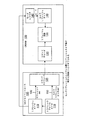
次に図面を参照すると、セルフリフレッシュ動作モードに入っている間のSoCメモリコントローラ(MC)100およびDRAM集積回路105が図1に示されており、DRAM105がそのリフレッシュサイクルを管理する間にMC100がスリープ動作モードに入る。一実施形態では、MC100は、最後のアクセス(読出し動作または書込み動作)がDRAM105上で実行されてからのアイドル期間を計時するトラフィックアイドルタイマ110を含む。アイドル期間がアイドルしきい値を超えない場合、MC100は、DRAM105内のリフレッシュサイクルのスケジューリングをMC100が制御するリフレッシュ動作モードで動作し続ける。そうするために、MC100は、DRAM105の最後のメモリコントローラによってトリガされたリフレッシュサイクルからの遅延を計時するリフレッシュタイマ115を含む。遅延がDRAM105のリフレッシュ間隔に等しい場合、リフレッシュタイマ115はリフレッシュコマンド(cmd)120をコマンドスケジューラ125にアサートする。それに応答して、コマンドスケジューラ125は、リフレッシュサイクルを実行するためにリフレッシュ回路135をトリガするようにDRAM105内のコマンドデコーダ130に命令する。このようにして、リフレッシュタイマ115は、リフレッシュ動作モード中にリフレッシュ間隔によって決定されるレートでDRAM105内のリフレッシュサイクルを定期的にトリガする。
Referring now to the drawings, the SoC memory controller (MC) 100 and DRAM integrated
トラフィックアイドルタイマ110のタイムアウトが、アクティビティの不足のためにアイドルしきい値を超えたことを示す場合、トラフィックアイドルタイマ110は、セルフリフレッシュコマンド(cmd)150をコマンドスケジューラ125にアサートし得る。次に、コマンドスケジューラ125は、DRAM105にセルフリフレッシュ動作モードに入るように命令するよう、コマンドデコーダ130に命令する。トラフィックアイドルタイマ110がセルフリフレッシュコマンド150をアサートすると同時に、トラフィックアイドルタイマ110はまた、最後のメモリコントローラによってトリガされたリフレッシュサイクルが発生した時をDRAM105に知らせるためにDRAM105内のモードレジスタ140に書き込むために、リフレッシュタイマ115をトリガする。この通信は、リフレッシュタイマ115が、最後の(最新の)メモリコントローラによってトリガされたリフレッシュサイクル以降に満了した時間、または現在のリフレッシュ間隔内の残りの時間をモードレジスタ140に書き込むことによって実行され得る。あるいは、リフレッシュタイマ115は、最新のメモリコントローラによってトリガされたリフレッシュサイクル以降の現在のリフレッシュ間隔の残りの部分(もしあれば)をデジタル化し得る。たとえば、リフレッシュタイマ115は、現在のリフレッシュ間隔の残りの部分の1/8の増分において見積もることができるように、3ビットデジタル化を使用し得る。あるいは、リフレッシュタイマ115は、4ビットデジタル化(1/16の増分)あるいはより低次またはより高次のデジタル化を使用し得る。以下の議論では、比較的少数のビットしか必要とせず、したがって帯域幅効率が良いので、リフレッシュタイマ115が、現在のリフレッシュ間隔のデジタル化された残りの部分をモードレジスタ140に書き込むという一般性を失うことなしに仮定する。
If the
次いで、DRAM105は、現在のリフレッシュ間隔のデジタル化された推定される残りの部分をモードレジスタ140からセルフリフレッシュタイマ145にロードすることによって、セルフリフレッシュ動作モードに入ることができる。たとえば、リフレッシュタイマ115が現在のリフレッシュ間隔の1/8が残っていることを示していた場合、セルフリフレッシュタイマ145は、DRAMリフレッシュ回路135内の最初のDRAMによってトリガされたセルフリフレッシュサイクルをトリガする前にリフレッシュ間隔のちょうど1/8までカウントダウンし得る。この最初のセルフリフレッシュサイクルをトリガした後、セルフリフレッシュタイマ145は、後続のセルフリフレッシュサイクルのトリガのために完全なリフレッシュ間隔からカウントダウンする。次いで、DRAM105は、SoCメモリコントローラ100が通常動作を再開し、スリープモードを終了するまで、そのセルフリフレッシュサイクルを管理する。
The
リフレッシュタイマ115はまた、リフレッシュ間隔のための現在の温度乗数(temperature multiplier)をDRAM105に通知し得る。DRAMメモリセル内のコンデンサからの漏れは、温度とともに増加する。したがって、メモリコントローラによってトリガされたリフレッシュサイクル内であろうと、DRAMによって制御されるセルフリフレッシュサイクル内であろうと、温度が上昇するにつれてリフレッシュ間隔を減少させることが有利であり得る。現在のリフレッシュ間隔の残りの部分と同様に、リフレッシュ間隔のこの減少もまた、ある数のビットを使用してデジタル化され、デジタル化された温度乗数によって表され得る。たとえば、温度乗数が3ビット数にデジタル化されていると仮定する。室温では、リフレッシュ間隔の減少が示されないので、デジタル化された温度乗数は1に等しくてもよい。温度が上昇するにつれて、デジタル化された温度乗数は徐々に1から減少する。したがって、リフレッシュタイマ115は、リフレッシュサイクルの残りの部分のメモリコントローラ100によるモードレジスタ140への書込みと同様に、デジタル化された温度乗数をモードレジスタ140またはDRAM105内の別のレジスタ(図示せず)に書き込むこともできる。
The
通常(アクティブ)動作を再開するためにスリープモードを終了するSoCメモリコントローラ100に応答して、セルフリフレッシュ動作モードからリフレッシュ動作モードへの移行において、セルフリフレッシュタイマ145は、図2に示されるように、現在のリフレッシュ間隔のデジタル化された残りの部分(もしあれば)をモードレジスタ140(または、別の適切なレジスタ)に書き込むことができる。次いで、リフレッシュタイマ115は、リフレッシュモードへの移行時に最初のリフレッシュサイクルのリフレッシュ間隔の残りの部分からカウントダウンするように、モードレジスタ140の内容を読み取ることができる。リフレッシュタイマ115が、モードレジスタ140からの読出しを通じて通知されたままの部分に応じた最初のリフレッシュサイクルをトリガした後、リフレッシュタイマ115は、任意の後続のメモリコントローラによってトリガされたリフレッシュサイクルのリフレッシュ間隔全体を使用して、セルフリフレッシュ動作モードへの別の移行までカウントダウンする。セルフリフレッシュタイマ145はまた、現在のデジタル温度乗数を、モードレジスタ140または別の類似のレジスタに書き込むことができる点に留意されたい。次いで、リフレッシュタイマ115は、モードレジスタ140からの残りのリフレッシュ間隔部分とともにこの乗数を使用する。たとえば、モードレジスタ140が、最後のDRAMによってトリガされたリフレッシュサイクルがリフレッシュ間隔の1/2前に行われたことを示すと仮定する。DRAM105が、上昇したDRAM温度のために温度乗数が1/2であることを示す場合、リフレッシュタイマ115は、デフォルト(室温)リフレッシュ間隔の1/2からではなく、上昇した温度からの減少のためにデフォルトリフレッシュ間隔の1/4からカウントダウンする。
In response to the
図3Aは、図1に関して説明したような、リフレッシュ動作モードからセルフリフレッシュ動作モードへのフローチャートである。本方法は、メモリコントローラがDRAMの現在のリフレッシュサイクル内の残りの部分を依然として有する間に、メモリコントローラがアクティブ動作モードからスリープ動作モードに移行する動作300を含む。図2のメモリコントローラ100のアクティブ動作モードからスリープ動作モードへの移行は、動作300の一例である。本方法はさらに、メモリコントローラから、スリープ動作モードに移行する前に、現在のリフレッシュサイクル内の残りの部分をDRAMに通信する動作305を含む。現在のリフレッシュサイクルの残りの部分を識別する、リフレッシュタイマ115によるモードレジスタ140への書込みは、動作305の一例である。最後に、本方法は、現在のリフレッシュサイクル内の残りの部分のDRAMにおけるカウントダウンに応答して、DRAM内のセルフリフレッシュサイクルをトリガする動作310を含む。セルフリフレッシュタイマ145におけるカウントダウンと、リフレッシュ回路135によるセルフリフレッシュサイクルの後続のトリガは、動作310の一例である。
FIG. 3A is a flowchart from the refresh operation mode to the self-refresh operation mode as described with reference to FIG. The method includes an
図3Bは、リフレッシュ動作モードからセルフリフレッシュ動作モードに入るための方法を示すフローチャートである。本方法は、メモリコントローラをスリープ動作モードからアクティブ動作モードに移行する動作315を含む。図2のメモリコントローラ100のスリープ動作モードからアクティブ動作モードへの移行は、動作315の一例である。本方法はまた、ダイナミックランダムアクセスメモリ(DRAM)から、DRAMの最新のDRAMによってトリガされたセルフリフレッシュ以降のセルフリフレッシュ間隔の残りの部分の表示をメモリコントローラにおいて受信する動作320を含む。リフレッシュタイマ115によるモードレジスタ140の読出しは、動作320の一例である。さらに、本方法は、メモリコントローラにおいて、セルフリフレッシュ間隔の残りの部分をカウントダウンする動作325を含む。モードレジスタ140から取り出されたセルフリフレッシュ間隔のリフレッシュタイマ115による残りの部分のカウントダウンは、動作325の一例である。最後に、本方法は、セルフリフレッシュ間隔の残りの部分のカウントダウンに応答して、メモリコントローラからDRAM内のリフレッシュサイクルをトリガする動作330を含む。DRAM105内のリフレッシュサイクルのコマンドスケジューラ125によるトリガは、動作330の一例である。
FIG. 3B is a flowchart illustrating a method for entering the self-refresh operation mode from the refresh operation mode. The method includes an
メモリコントローラ100は、図4に示されるように、デバイス400内のシステムオンチップ(SoC)405内に組み込まれ得る。デバイス400は、セルラーフォン、スマートフォン、携帯情報端末、タブレットコンピュータ、ラップトップコンピュータ、デジタルカメラ、ハンドヘルドゲーミングデバイス、または他の適切なデバイスを含んでもよい。SoC405内のメモリコントローラ100は、システムバス415を介してDRAM105と通信する。SoCはまた、システムバス415を介してセンサなどの周辺デバイス410と通信する。ディスプレイコントローラ425も、システムバス415に結合する。今度は、ディスプレイコントローラ425は、ディスプレイ435を駆動するビデオプロセッサ430に結合する。SoC405はまた、DRAM105の温度を監視するために、DRAM105内またはその近傍に温度センサ440を含み得る。
The
本開示に関連して説明される方法またはアルゴリズムのステップは、ハードウェアにおいて、プロセッサによって実行されるソフトウェアモジュールにおいて、またはその2つの組合せにおいて直接的に実施され得る。ソフトウェアにおいて実装される場合、機能は、1つまたは複数の命令あるいはコンピュータ可読媒体上のコードに格納され得る。例示的なコンピュータ可読媒体は、プロセッサがコンピュータ可読媒体から情報を読み出し、コンピュータ可読媒体に情報を書き込むことができるように、プロセッサに結合される。あるいは、コンピュータ可読媒体は、プロセッサと一体であってもよい。 The method or algorithm steps described in connection with this disclosure may be implemented directly in hardware, in software modules executed by a processor, or in a combination of the two. If implemented in software, the functions may be stored in one or more instructions or code on a computer-readable medium. An exemplary computer readable medium is coupled to the processor such that the processor can read information from, and write information to, the computer readable medium. In the alternative, the computer readable medium may be integral to the processor.
当業者であれば理解するように、当面の特定の用途に応じて、本開示の範囲から逸脱することなしに、本開示のデバイスの材料、装置、構成、および使用方法に多くの修正、置換、および変形が行われ得る。これに照らして、本明細書において図示および説明されている特定の実施形態はそのいくつかの例としてのものにすぎないため、本開示の範囲はそれらの特定の実施形態の範囲に限定されるべきではなく、むしろ、下記に添付されている特許請求の範囲およびそれらの機能的な均等物の範囲と完全に同等であるべきである。 As will be appreciated by those skilled in the art, many modifications and substitutions may be made to the materials, apparatus, configurations and methods of use of the devices of the present disclosure without departing from the scope of the present disclosure, depending on the particular application at hand. , And variations can be made. In light of this, the specific embodiments illustrated and described herein are merely some examples thereof, and the scope of the present disclosure is limited to the scope of those specific embodiments. Rather, it should be fully equivalent to the scope of the claims appended hereto and their functional equivalents.
100 SoCメモリコントローラ(MC)
105 DRAM集積回路
110 トラフィックアイドルタイマ
115 リフレッシュタイマ
120 リフレッシュコマンド(cmd)
125 コマンドスケジューラ
130 コマンドデコーダ
135 リフレッシュ回路
140 モードレジスタ
145 セルフリフレッシュタイマ
150 セルフリフレッシュコマンド(cmd)
300 動作
305 動作
310 動作
315 動作
320 動作
325 動作
330 動作
400 デバイス
405 システムオンチップ(SoC)
410 周辺デバイス
415 システムバス
425 ディスプレイコントローラ
430 ビデオプロセッサ
435 ディスプレイ
440 温度センサ
100 SoC memory controller (MC)
105 DRAM integrated circuit
110 Traffic idle timer
115 Refresh timer
120 Refresh command (cmd)
125 Command scheduler
130 Command decoder
135 Refresh circuit
140 Mode register
145 Self-refresh timer
150 Self-refresh command (cmd)
300 operation
305 operation
310 Operation
315 operation
320 operation
325 operation
330 Operation
400 devices
405 System on chip (SoC)
410 Peripheral devices
415 system bus
425 display controller
430 video processor
435 display
440 temperature sensor
Claims (20)
DRAMの最新のDRAMによってトリガされたセルフリフレッシュ以降のセルフリフレッシュ間隔の残りの部分の表示を前記メモリコントローラにおいて受信するステップと、
前記メモリコントローラにおいて、前記セルフリフレッシュ間隔の前記残りの部分をカウントダウンするステップと、
前記セルフリフレッシュ間隔の前記残りの部分の前記カウントダウンに応答して、前記メモリコントローラから前記DRAM内の最初のリフレッシュサイクルをトリガするステップと
を含む、方法。 A method of transitioning a memory controller from a sleep operation mode to an active operation mode,
Receiving an indication at the memory controller of a remaining portion of a self-refresh interval after a self-refresh triggered by the latest DRAM of the DRAM; and
Counting down the remaining portion of the self-refresh interval in the memory controller;
Triggering a first refresh cycle in the DRAM from the memory controller in response to the countdown of the remaining portion of the self-refresh interval.
前記アイドル期間を計時する前記ステップがしきい値を超えたことに応答して、前記メモリコントローラを前記アクティブ動作モードから前記スリープ動作モードに戻すステップと
をさらに含む、請求項1に記載の方法。 Timing the idle period of the memory controller;
2. The method of claim 1, further comprising returning the memory controller from the active mode of operation to the sleep mode of operation in response to the step of timing the idle period exceeding a threshold value.
前記リフレッシュタイマによる前記セルフリフレッシュ間隔の前記部分の前記カウントダウンに応答して、前記DRAM内の最初のメモリコントローラによってトリガされたリフレッシュサイクルをトリガするように構成されたコマンドスケジューラと
を備える、メモリコントローラ。 A refresh timer configured to count down a portion of the self-refresh interval in response to an indication from the dynamic random access memory (DRAM) when the latest self-refresh cycle triggered by the DRAM occurs;
And a command scheduler configured to trigger a refresh cycle triggered by the first memory controller in the DRAM in response to the countdown of the portion of the self-refresh interval by the refresh timer.
メモリコントローラからの表示に応答して、前記メモリコントローラによってトリガされた最新のリフレッシュサイクルが発生した時に、スリープ動作モードに移行するセルフリフレッシュ間隔の残りの部分をカウントダウンするように構成されたセルフリフレッシュタイマと、
前記セルフリフレッシュタイマが前記セルフリフレッシュ間隔の前記残りの部分をカウントダウンすることに応答して前記DRAMをリフレッシュするように構成されたリフレッシュ回路と
を備える、ダイナミックランダムアクセスメモリ(DRAM)。 Dynamic random access memory (DRAM)
A self-refresh timer configured to count down the remaining portion of the self-refresh interval that transitions to a sleep operating mode when the latest refresh cycle triggered by the memory controller occurs in response to an indication from the memory controller When,
A dynamic random access memory (DRAM) comprising: a refresh circuit configured to refresh the DRAM in response to the self-refresh timer counting down the remaining portion of the self-refresh interval.
前記スリープ動作モードへの前記移行の前に、前記メモリコントローラから前記現在のリフレッシュサイクル内の残りの前記部分を前記DRAMに通信するステップと、
前記現在のリフレッシュサイクル内の残りの前記部分の前記DRAMにおけるカウントダウンに応答して、前記DRAM内のセルフリフレッシュサイクルをトリガするステップと
を含む、方法。 Transitioning the memory controller from an active operating mode to a sleep operating mode while the memory controller still has the rest of the DRAM's current refresh cycle;
Communicating the remaining portion of the current refresh cycle from the memory controller to the DRAM prior to the transition to the sleep mode of operation;
Triggering a self-refresh cycle in the DRAM in response to a countdown in the DRAM of the remaining portion of the current refresh cycle.
前記メモリコントローラにおいて、前記メモリコントローラが前記アクティブ動作モードに戻る前に、最後のセルフリフレッシュサイクルがトリガされた時の表示を前記DRAMから読み出すステップと
をさらに含む、請求項17に記載の方法。 Returning the memory controller from the sleep operation mode to the active operation mode;
18. The method of claim 17, further comprising: reading from the DRAM when the last self-refresh cycle is triggered before the memory controller returns to the active mode of operation at the memory controller.
Applications Claiming Priority (5)
| Application Number | Priority Date | Filing Date | Title |
|---|---|---|---|
| US201562236008P | 2015-10-01 | 2015-10-01 | |
| US62/236,008 | 2015-10-01 | ||
| US15/246,371 | 2016-08-24 | ||
| US15/246,371 US9875785B2 (en) | 2015-10-01 | 2016-08-24 | Refresh timer synchronization between memory controller and memory |
| PCT/US2016/048771 WO2017058417A1 (en) | 2015-10-01 | 2016-08-25 | Refresh timer synchronization between memory controller and memory |
Publications (2)
| Publication Number | Publication Date |
|---|---|
| JP2018530098A true JP2018530098A (en) | 2018-10-11 |
| JP2018530098A5 JP2018530098A5 (en) | 2019-09-19 |
Family
ID=56852438
Family Applications (1)
| Application Number | Title | Priority Date | Filing Date |
|---|---|---|---|
| JP2018516132A Pending JP2018530098A (en) | 2015-10-01 | 2016-08-25 | Refresh timer synchronization between memory controller and memory |
Country Status (7)
| Country | Link |
|---|---|
| US (1) | US9875785B2 (en) |
| EP (1) | EP3357065B1 (en) |
| JP (1) | JP2018530098A (en) |
| KR (1) | KR102593418B1 (en) |
| CN (1) | CN108140406B (en) |
| BR (1) | BR112018006477B1 (en) |
| WO (1) | WO2017058417A1 (en) |
Families Citing this family (10)
| Publication number | Priority date | Publication date | Assignee | Title |
|---|---|---|---|---|
| US20180061484A1 (en) * | 2016-08-29 | 2018-03-01 | Apple Inc. | Systems and Methods for Memory Refresh Timing |
| US20190074051A1 (en) * | 2017-09-07 | 2019-03-07 | Mediatek Inc. | Memory system and refresh control method thereof |
| US10489316B1 (en) | 2018-06-04 | 2019-11-26 | Micron Technology, Inc. | Methods for performing multiple memory operations in response to a single command and memory devices and systems employing the same |
| KR102578002B1 (en) | 2018-07-03 | 2023-09-14 | 에스케이하이닉스 주식회사 | Memory system and operating method thereof |
| US10685722B1 (en) * | 2019-01-24 | 2020-06-16 | Western Digital Technologies, Inc. | Method and system for improving performance of a storage device using asynchronous independent plane read functionality |
| US11250902B2 (en) * | 2019-09-26 | 2022-02-15 | Intel Corporation | Method and apparatus to reduce power consumption for refresh of memory devices on a memory module |
| KR20220003837A (en) * | 2020-07-02 | 2022-01-11 | 에스케이하이닉스 주식회사 | Storage device and operating method thereof |
| KR20220031793A (en) | 2020-09-03 | 2022-03-14 | 삼성전자주식회사 | Memory device, memory system having the same, controller for controlling the same, and operating methed thereof |
| KR20220091162A (en) | 2020-12-23 | 2022-06-30 | 삼성전자주식회사 | Memory device and method for refreshing operation irrelevant to refresh rate multipliers for temperatatures |
| TWI740773B (en) * | 2021-01-27 | 2021-09-21 | 華邦電子股份有限公司 | Semiconductor memory device |
Family Cites Families (30)
| Publication number | Priority date | Publication date | Assignee | Title |
|---|---|---|---|---|
| JPH07182857A (en) * | 1993-12-24 | 1995-07-21 | Toshiba Corp | Microcomputer system |
| JPH09213071A (en) * | 1996-02-02 | 1997-08-15 | Hitachi Ltd | Semiconductor memory |
| US5808952A (en) * | 1996-10-28 | 1998-09-15 | Silicon Magic Corporation | Adaptive auto refresh |
| US6212599B1 (en) * | 1997-11-26 | 2001-04-03 | Intel Corporation | Method and apparatus for a memory control system including a secondary controller for DRAM refresh during sleep mode |
| US6118719A (en) * | 1998-05-20 | 2000-09-12 | International Business Machines Corporation | Self-initiated self-refresh mode for memory modules |
| CN1184644C (en) * | 2001-03-16 | 2005-01-12 | 矽统科技股份有限公司 | Memory updating system |
| US6693837B2 (en) * | 2002-04-23 | 2004-02-17 | Micron Technology, Inc. | System and method for quick self-refresh exit with transitional refresh |
| JP4246971B2 (en) * | 2002-07-15 | 2009-04-02 | 富士通マイクロエレクトロニクス株式会社 | Semiconductor memory |
| KR100529033B1 (en) * | 2003-05-23 | 2005-11-17 | 주식회사 하이닉스반도체 | Synchronous semiconductor memory device |
| US7236416B2 (en) * | 2004-05-21 | 2007-06-26 | Qualcomm Incorporated | Method and system for controlling refresh in volatile memories |
| US7088633B2 (en) | 2004-05-27 | 2006-08-08 | Qualcomm Incorporated | Method and system for providing seamless self-refresh for directed bank refresh in volatile memories |
| US7206244B2 (en) * | 2004-12-01 | 2007-04-17 | Freescale Semiconductor, Inc. | Temperature based DRAM refresh |
| KR100655076B1 (en) * | 2005-01-20 | 2006-12-08 | 삼성전자주식회사 | Method for outputting internal temperature data in semiconductor memory device and internal temperature data circuit therefor |
| US9384818B2 (en) | 2005-04-21 | 2016-07-05 | Violin Memory | Memory power management |
| JP4516483B2 (en) * | 2005-06-07 | 2010-08-04 | 富士通セミコンダクター株式会社 | Semiconductor memory device and information processing system |
| US7313047B2 (en) * | 2006-02-23 | 2007-12-25 | Hynix Semiconductor Inc. | Dynamic semiconductor memory with improved refresh mechanism |
| CN101000798B (en) * | 2007-01-12 | 2010-05-19 | 威盛电子股份有限公司 | Memory updating method and memory updating system |
| US8392650B2 (en) * | 2010-04-01 | 2013-03-05 | Intel Corporation | Fast exit from self-refresh state of a memory device |
| US9053812B2 (en) * | 2010-09-24 | 2015-06-09 | Intel Corporation | Fast exit from DRAM self-refresh |
| US9292426B2 (en) * | 2010-09-24 | 2016-03-22 | Intel Corporation | Fast exit from DRAM self-refresh |
| US10157657B2 (en) * | 2012-08-28 | 2018-12-18 | Rambus Inc. | Selective refresh with software components |
| KR20140076735A (en) * | 2012-12-13 | 2014-06-23 | 삼성전자주식회사 | Volatile memory devices and memory systems |
| US9704557B2 (en) * | 2013-09-25 | 2017-07-11 | Qualcomm Incorporated | Method and apparatus for storing retention time profile information based on retention time and temperature |
| US9001608B1 (en) * | 2013-12-06 | 2015-04-07 | Intel Corporation | Coordinating power mode switching and refresh operations in a memory device |
| KR20160122586A (en) * | 2015-04-14 | 2016-10-24 | 에스케이하이닉스 주식회사 | Semiconductor device and semiconductor system using the same |
| KR102326018B1 (en) * | 2015-08-24 | 2021-11-12 | 삼성전자주식회사 | Memory system |
| KR102354987B1 (en) * | 2015-10-22 | 2022-01-24 | 삼성전자주식회사 | Refresh method for controlling self refresh cycle with temperature |
| KR102393426B1 (en) * | 2015-11-10 | 2022-05-04 | 에스케이하이닉스 주식회사 | Semiconductor device |
| US9721640B2 (en) * | 2015-12-09 | 2017-08-01 | Intel Corporation | Performance of additional refresh operations during self-refresh mode |
| KR102419535B1 (en) * | 2016-03-18 | 2022-07-13 | 에스케이하이닉스 주식회사 | Memory device |
-
2016
- 2016-08-24 US US15/246,371 patent/US9875785B2/en active Active
- 2016-08-25 BR BR112018006477-7A patent/BR112018006477B1/en active IP Right Grant
- 2016-08-25 WO PCT/US2016/048771 patent/WO2017058417A1/en active Application Filing
- 2016-08-25 CN CN201680058030.5A patent/CN108140406B/en active Active
- 2016-08-25 EP EP16759956.2A patent/EP3357065B1/en active Active
- 2016-08-25 KR KR1020187012415A patent/KR102593418B1/en active IP Right Grant
- 2016-08-25 JP JP2018516132A patent/JP2018530098A/en active Pending
Also Published As
| Publication number | Publication date |
|---|---|
| BR112018006477A2 (en) | 2018-10-09 |
| CN108140406A (en) | 2018-06-08 |
| BR112018006477B1 (en) | 2023-03-14 |
| US9875785B2 (en) | 2018-01-23 |
| EP3357065B1 (en) | 2019-06-26 |
| CN108140406B (en) | 2022-03-22 |
| US20170098470A1 (en) | 2017-04-06 |
| KR20180063230A (en) | 2018-06-11 |
| WO2017058417A1 (en) | 2017-04-06 |
| KR102593418B1 (en) | 2023-10-23 |
| EP3357065A1 (en) | 2018-08-08 |
Similar Documents
| Publication | Publication Date | Title |
|---|---|---|
| JP2018530098A (en) | Refresh timer synchronization between memory controller and memory | |
| CN108196809B (en) | Memory power savings in idle display situations | |
| US9984737B2 (en) | Reduction of power consumption in memory devices during refresh modes | |
| US20140129757A1 (en) | System and method for dynamic memory power management | |
| US10175995B1 (en) | Device hibernation control | |
| US20200348746A1 (en) | Power-Conserving Cache Memory Usage | |
| EP3172635B1 (en) | Ultra low power architecture to support always on path to memory | |
| JP2017529600A (en) | Power management for memory access in system on chip | |
| JP2006018797A (en) | Method for reducing standby electricity of integrated circuit device, method for operating memory array with cache of integrated circuit, and integrated circuit device | |
| US10345885B2 (en) | Power control of a memory device through a sideband channel of a memory bus | |
| US11520498B2 (en) | Memory management to improve power performance | |
| KR102653415B1 (en) | Memory controller and memory system including the same | |
| US9547361B2 (en) | Methods and apparatuses for memory power reduction | |
| JP6054203B2 (en) | Information processing apparatus, device control method, and program | |
| US10268486B1 (en) | Expedited resume process from hibernation | |
| US10430096B2 (en) | Hybrid storage device, computer, control device, and power consumption reduction method | |
| CN105824760B (en) | Storage device and power control method thereof | |
| US10872651B2 (en) | Volatile memory device and self-refresh method by enabling a voltage boost signal | |
| TWI637387B (en) | Non-volatile memory device and self-refresh method thereof | |
| KR20220040822A (en) | Low power system-on-chip and operation method thereof |
Legal Events
| Date | Code | Title | Description |
|---|---|---|---|
| A521 | Request for written amendment filed |
Free format text: JAPANESE INTERMEDIATE CODE: A523 Effective date: 20190805 |
|
| A621 | Written request for application examination |
Free format text: JAPANESE INTERMEDIATE CODE: A621 Effective date: 20190805 |
|
| A977 | Report on retrieval |
Free format text: JAPANESE INTERMEDIATE CODE: A971007 Effective date: 20200709 |
|
| A131 | Notification of reasons for refusal |
Free format text: JAPANESE INTERMEDIATE CODE: A131 Effective date: 20200824 |
|
| A02 | Decision of refusal |
Free format text: JAPANESE INTERMEDIATE CODE: A02 Effective date: 20210405 |