JP2018521612A - Method and apparatus for mitigating phase shift fields - Google Patents
Method and apparatus for mitigating phase shift fields Download PDFInfo
- Publication number
- JP2018521612A JP2018521612A JP2017557085A JP2017557085A JP2018521612A JP 2018521612 A JP2018521612 A JP 2018521612A JP 2017557085 A JP2017557085 A JP 2017557085A JP 2017557085 A JP2017557085 A JP 2017557085A JP 2018521612 A JP2018521612 A JP 2018521612A
- Authority
- JP
- Japan
- Prior art keywords
- magnetic field
- coil
- phase
- power transmission
- wireless power
- Prior art date
- Legal status (The legal status is an assumption and is not a legal conclusion. Google has not performed a legal analysis and makes no representation as to the accuracy of the status listed.)
- Pending
Links
- 238000000034 method Methods 0.000 title claims abstract description 69
- 230000000116 mitigating effect Effects 0.000 title description 29
- 230000010363 phase shift Effects 0.000 title description 28
- 230000005540 biological transmission Effects 0.000 claims description 217
- 239000002184 metal Substances 0.000 claims description 34
- 229910052751 metal Inorganic materials 0.000 claims description 34
- 229910000859 α-Fe Inorganic materials 0.000 claims description 17
- 230000004044 response Effects 0.000 claims description 15
- 238000012546 transfer Methods 0.000 description 31
- 230000000694 effects Effects 0.000 description 28
- 238000001514 detection method Methods 0.000 description 25
- 238000010586 diagram Methods 0.000 description 25
- 239000003990 capacitor Substances 0.000 description 18
- 230000008901 benefit Effects 0.000 description 12
- 230000001965 increasing effect Effects 0.000 description 12
- 230000000670 limiting effect Effects 0.000 description 11
- 230000008859 change Effects 0.000 description 10
- 238000010168 coupling process Methods 0.000 description 8
- 238000006243 chemical reaction Methods 0.000 description 7
- 230000008878 coupling Effects 0.000 description 7
- 238000005859 coupling reaction Methods 0.000 description 7
- 238000013461 design Methods 0.000 description 7
- 230000002829 reductive effect Effects 0.000 description 7
- 230000002441 reversible effect Effects 0.000 description 7
- 230000006698 induction Effects 0.000 description 5
- 238000011084 recovery Methods 0.000 description 5
- 230000005672 electromagnetic field Effects 0.000 description 4
- 230000006870 function Effects 0.000 description 4
- 230000009471 action Effects 0.000 description 3
- 238000004364 calculation method Methods 0.000 description 3
- 238000004891 communication Methods 0.000 description 3
- 238000005516 engineering process Methods 0.000 description 3
- 230000001939 inductive effect Effects 0.000 description 3
- 230000009467 reduction Effects 0.000 description 3
- 230000011664 signaling Effects 0.000 description 3
- 230000005684 electric field Effects 0.000 description 2
- 239000000463 material Substances 0.000 description 2
- 230000004048 modification Effects 0.000 description 2
- 238000012986 modification Methods 0.000 description 2
- 230000003287 optical effect Effects 0.000 description 2
- 230000003044 adaptive effect Effects 0.000 description 1
- 238000007792 addition Methods 0.000 description 1
- 238000003491 array Methods 0.000 description 1
- 230000002238 attenuated effect Effects 0.000 description 1
- 230000001413 cellular effect Effects 0.000 description 1
- 239000004020 conductor Substances 0.000 description 1
- 230000004907 flux Effects 0.000 description 1
- 238000002847 impedance measurement Methods 0.000 description 1
- 239000006249 magnetic particle Substances 0.000 description 1
- 150000002739 metals Chemical class 0.000 description 1
- 230000010355 oscillation Effects 0.000 description 1
- 230000036961 partial effect Effects 0.000 description 1
- 239000002245 particle Substances 0.000 description 1
- 230000002093 peripheral effect Effects 0.000 description 1
- 238000012545 processing Methods 0.000 description 1
- 230000005855 radiation Effects 0.000 description 1
Images


Classifications
-
- H—ELECTRICITY
- H02—GENERATION; CONVERSION OR DISTRIBUTION OF ELECTRIC POWER
- H02J—CIRCUIT ARRANGEMENTS OR SYSTEMS FOR SUPPLYING OR DISTRIBUTING ELECTRIC POWER; SYSTEMS FOR STORING ELECTRIC ENERGY
- H02J50/00—Circuit arrangements or systems for wireless supply or distribution of electric power
- H02J50/10—Circuit arrangements or systems for wireless supply or distribution of electric power using inductive coupling
- H02J50/12—Circuit arrangements or systems for wireless supply or distribution of electric power using inductive coupling of the resonant type
-
- H—ELECTRICITY
- H01—ELECTRIC ELEMENTS
- H01F—MAGNETS; INDUCTANCES; TRANSFORMERS; SELECTION OF MATERIALS FOR THEIR MAGNETIC PROPERTIES
- H01F27/00—Details of transformers or inductances, in general
- H01F27/34—Special means for preventing or reducing unwanted electric or magnetic effects, e.g. no-load losses, reactive currents, harmonics, oscillations, leakage fields
- H01F27/36—Electric or magnetic shields or screens
- H01F27/363—Electric or magnetic shields or screens made of electrically conductive material
-
- H—ELECTRICITY
- H01—ELECTRIC ELEMENTS
- H01F—MAGNETS; INDUCTANCES; TRANSFORMERS; SELECTION OF MATERIALS FOR THEIR MAGNETIC PROPERTIES
- H01F27/00—Details of transformers or inductances, in general
- H01F27/34—Special means for preventing or reducing unwanted electric or magnetic effects, e.g. no-load losses, reactive currents, harmonics, oscillations, leakage fields
- H01F27/36—Electric or magnetic shields or screens
- H01F27/366—Electric or magnetic shields or screens made of ferromagnetic material
-
- H—ELECTRICITY
- H01—ELECTRIC ELEMENTS
- H01F—MAGNETS; INDUCTANCES; TRANSFORMERS; SELECTION OF MATERIALS FOR THEIR MAGNETIC PROPERTIES
- H01F38/00—Adaptations of transformers or inductances for specific applications or functions
- H01F38/14—Inductive couplings
-
- H—ELECTRICITY
- H02—GENERATION; CONVERSION OR DISTRIBUTION OF ELECTRIC POWER
- H02J—CIRCUIT ARRANGEMENTS OR SYSTEMS FOR SUPPLYING OR DISTRIBUTING ELECTRIC POWER; SYSTEMS FOR STORING ELECTRIC ENERGY
- H02J50/00—Circuit arrangements or systems for wireless supply or distribution of electric power
- H02J50/20—Circuit arrangements or systems for wireless supply or distribution of electric power using microwaves or radio frequency waves
-
- H—ELECTRICITY
- H02—GENERATION; CONVERSION OR DISTRIBUTION OF ELECTRIC POWER
- H02J—CIRCUIT ARRANGEMENTS OR SYSTEMS FOR SUPPLYING OR DISTRIBUTING ELECTRIC POWER; SYSTEMS FOR STORING ELECTRIC ENERGY
- H02J50/00—Circuit arrangements or systems for wireless supply or distribution of electric power
- H02J50/70—Circuit arrangements or systems for wireless supply or distribution of electric power involving the reduction of electric, magnetic or electromagnetic leakage fields
-
- H—ELECTRICITY
- H02—GENERATION; CONVERSION OR DISTRIBUTION OF ELECTRIC POWER
- H02J—CIRCUIT ARRANGEMENTS OR SYSTEMS FOR SUPPLYING OR DISTRIBUTING ELECTRIC POWER; SYSTEMS FOR STORING ELECTRIC ENERGY
- H02J50/00—Circuit arrangements or systems for wireless supply or distribution of electric power
- H02J50/80—Circuit arrangements or systems for wireless supply or distribution of electric power involving the exchange of data, concerning supply or distribution of electric power, between transmitting devices and receiving devices
-
- H—ELECTRICITY
- H02—GENERATION; CONVERSION OR DISTRIBUTION OF ELECTRIC POWER
- H02J—CIRCUIT ARRANGEMENTS OR SYSTEMS FOR SUPPLYING OR DISTRIBUTING ELECTRIC POWER; SYSTEMS FOR STORING ELECTRIC ENERGY
- H02J50/00—Circuit arrangements or systems for wireless supply or distribution of electric power
- H02J50/90—Circuit arrangements or systems for wireless supply or distribution of electric power involving detection or optimisation of position, e.g. alignment
-
- H—ELECTRICITY
- H02—GENERATION; CONVERSION OR DISTRIBUTION OF ELECTRIC POWER
- H02J—CIRCUIT ARRANGEMENTS OR SYSTEMS FOR SUPPLYING OR DISTRIBUTING ELECTRIC POWER; SYSTEMS FOR STORING ELECTRIC ENERGY
- H02J7/00—Circuit arrangements for charging or depolarising batteries or for supplying loads from batteries
- H02J7/00032—Circuit arrangements for charging or depolarising batteries or for supplying loads from batteries characterised by data exchange
- H02J7/00034—Charger exchanging data with an electronic device, i.e. telephone, whose internal battery is under charge
-
- H04B5/26—
-
- H04B5/266—
-
- H04B5/79—
-
- H—ELECTRICITY
- H01—ELECTRIC ELEMENTS
- H01F—MAGNETS; INDUCTANCES; TRANSFORMERS; SELECTION OF MATERIALS FOR THEIR MAGNETIC PROPERTIES
- H01F27/00—Details of transformers or inductances, in general
- H01F27/34—Special means for preventing or reducing unwanted electric or magnetic effects, e.g. no-load losses, reactive currents, harmonics, oscillations, leakage fields
- H01F27/36—Electric or magnetic shields or screens
Abstract
本発明は、ワイヤレス電力を供給するための方法および装置について説明する。開示する方法および装置は、少なくとも1つのループを有する第1のコイルであって、少なくとも1つのループが、少なくとも1つのループの境界の内側に内側領域を形成し、少なくとも1つのループの境界の外側に外側領域を形成し、第1のコイルが、ワイヤレス電力デバイスを充電するかまたはワイヤレス電力デバイスに電力を供給するための第1の交番磁界を生成するように構成され、第1の交番磁界が、第1の位相を有する第1の磁界成分を内側領域内に有し、第1の交番磁界がさらに、第2の位相を有する第2の磁界成分を外側領域内に有し、第2の位相が第1の位相とは異なる第1のコイルからなる。いくつかの態様では、この方法および装置は、一部を外側領域内に含む第2のコイルであって、第2の磁界成分を小さくするように構成された第2のコイルをさらに備える。The present invention describes a method and apparatus for supplying wireless power. The disclosed method and apparatus is a first coil having at least one loop, the at least one loop forming an inner region inside the boundary of the at least one loop, and outside the boundary of the at least one loop The first coil is configured to generate a first alternating magnetic field for charging or supplying power to the wireless power device, wherein the first alternating magnetic field is A first magnetic field component having a first phase in the inner region, a first alternating magnetic field further having a second magnetic field component having a second phase in the outer region, and a second The first coil is different in phase from the first phase. In some aspects, the method and apparatus further comprises a second coil that includes a portion in the outer region, the second coil configured to reduce the second magnetic field component.
Description
説明する技術は、一般に、ワイヤレス電力に関する。より詳細には、本開示は、送電コイルの周囲におけるフィールドの位相ずれ作用を軽減することを含むワイヤレス電力伝達に関係するデバイス、システム、および方向を対象とする。 The described techniques generally relate to wireless power. More particularly, the present disclosure is directed to devices, systems, and directions related to wireless power transfer including mitigating field out-of-phase effects around a power transmission coil.
充電式バッテリーによって電力を供給される電子デバイスの数および種類が増大している。そのようなデバイスには、モバイルフォン、電気車両、ポータブル音楽プレーヤ、ラップトップコンピュータ、タブレットコンピュータ、コンピュータ周辺デバイス、通信デバイス(たとえば、Bluetooth(登録商標)デバイス)、デジタルカメラ、補聴器などが含まれる。バッテリー技術は向上してきたが、バッテリー電源式電子デバイスは、より多くの電力量をますます必要とし消費しているので、頻繁に再充電する必要がある。充電式デバイスは、多くの場合に、電源に物理的に接続されるケーブルまたは他の同様のコネクタを必要とする有線接続によって充電される。ケーブルおよび同様のコネクタは、不便で扱いにくいことがあり、他の欠点を有する場合もある。充電式電子デバイスを充電するのに使用されることになる電力を自由空間において伝達することができるワイヤレス充電システムは、有線式の充電ソリューションの欠点の一部を克服する可能性がある。したがって、充電式電子デバイスを充電するための電力を効率的かつ安全に伝達するワイヤレス充電システムおよびワイヤレス充電方法が望ましい。 An increasing number and types of electronic devices are powered by rechargeable batteries. Such devices include mobile phones, electric vehicles, portable music players, laptop computers, tablet computers, computer peripheral devices, communication devices (eg, Bluetooth® devices), digital cameras, hearing aids, and the like. While battery technology has improved, battery-powered electronic devices are increasingly consuming and consuming more power and need to be recharged frequently. Rechargeable devices are often charged by a wired connection that requires a cable or other similar connector that is physically connected to a power source. Cables and similar connectors may be inconvenient and cumbersome and may have other drawbacks. A wireless charging system that can transmit power in free space to be used to charge a rechargeable electronic device can overcome some of the shortcomings of wired charging solutions. Accordingly, a wireless charging system and wireless charging method that efficiently and safely transfers power for charging a rechargeable electronic device is desirable.
本発明のシステム、方法、およびデバイスはそれぞれ、いくつかの態様を有し、どの態様も単独で本発明の望ましい属性を担うわけではない。次に、以下の特許請求の範囲によって表現されるような本発明の範囲を限定することなく、いくつかの特徴について簡単に説明する。この説明を考察した後、また特に「発明を実施するための形態」と題するセクションを読んだ後、本発明の様々な実施形態の特徴が、ワイヤレス電力システムにおける電力およびインピーダンスの測定の改善を含む利点をどのようにもたらすのかが理解されよう。 Each of the systems, methods, and devices of the present invention has several aspects, and none of the aspects alone carry the desirable attributes of the present invention. Several features will now be described briefly without limiting the scope of the invention as expressed by the following claims. After considering this description, and particularly after reading the section entitled “Mode for Carrying Out the Invention”, features of various embodiments of the present invention include improved power and impedance measurements in wireless power systems. You will understand how it brings benefits.
本開示の一態様は、ワイヤレス電力を供給するための装置を含む。この装置は、ワイヤレス電力デバイスを充電するためのフィールドを生成するように構成された送電コイルを備える。この装置は、送電コイルの周囲の少なくとも一部を囲み、送電コイルの周囲におけるフィールドの位相ずれ(out-of-phase)作用を軽減させるように構成された補償コイルをさらに備える。いくつかの態様では、フィールドは磁界であり、位相ずれ作用は逆位相フィールドである。 One aspect of the present disclosure includes an apparatus for supplying wireless power. The apparatus comprises a power transmission coil configured to generate a field for charging a wireless power device. The apparatus further includes a compensation coil that surrounds at least a portion of the periphery of the power transmission coil and is configured to reduce field out-of-phase effects around the power transmission coil. In some aspects, the field is a magnetic field and the phase shift effect is an anti-phase field.
開示する別の態様は、ワイヤレス電力を供給するための方法である。この方法は、ワイヤレス電力デバイスを充電するためのフィールドを送電コイルによって生成するステップを含む。この方法は、送電コイルの周囲におけるフィールドの位相ずれ作用を補償コイルによって低減させるステップであって、補償コイルが送電コイルの周囲の少なくとも一部を囲む、ステップをさらに含む。いくつかの態様では、フィールドは磁界であり、位相ずれ作用は逆位相フィールドである。いくつかの態様では、非一時コンピュータ可読媒体は、実行されたときに、上述の方法を実行する命令を含んでもよい。 Another aspect disclosed is a method for supplying wireless power. The method includes generating a field for charging a wireless power device with a power transmission coil. The method further includes the step of reducing the out-of-phase effect of the field around the power transmission coil with the compensation coil, the compensation coil surrounding at least a portion of the circumference of the power transmission coil. In some aspects, the field is a magnetic field and the phase shift effect is an anti-phase field. In some aspects, the non-transitory computer readable medium may include instructions that, when executed, perform the methods described above.
開示する別の態様は、ワイヤレス電力を供給するためのデバイスである。このデバイスは、ワイヤレス電力デバイスを充電するためのフィールドを生成するための手段を含む。このデバイスは、生成するための手段の周囲におけるフィールドの位相ずれ作用を低減させるための手段であって、生成するための手段の周囲の少なくとも一部を囲む手段をさらに備える。いくつかの態様では、このフィールドは磁界であり、位相ずれ作用は逆位相フィールドである。いくつかの態様では、生成するための手段は、送電コイルを備えてもよい。いくつかの態様では、低減させるための手段は、補償コイルを備えてもよい。 Another aspect disclosed is a device for supplying wireless power. The device includes means for generating a field for charging the wireless power device. The device further comprises means for reducing the out-of-phase effect of the field around the means for generating and surrounding at least a portion of the periphery of the means for generating. In some aspects, this field is a magnetic field and the phase shift effect is an anti-phase field. In some aspects, the means for generating may comprise a power transmission coil. In some aspects, the means for reducing may comprise a compensation coil.
本開示の別の態様は、電力をワイヤレスに伝達するための装置を含む。この装置は、少なくとも1つのループを有する第1のコイルであって、少なくとも1つのループが、少なくとも1つのループの境界の内側に内側領域を形成し、少なくとも1つのループの境界の外側に外側領域を形成し、第1のコイルが、ワイヤレス電力デバイスを充電するかまたはワイヤレス電力デバイスに電力を供給するための第1の交番磁界を生成するように構成され、第1の交番磁界が、第1の位相を有する第1の磁界成分を内側領域内に有し、第1の交番磁界がさらに、第2の位相を有する第2の磁界成分を外側領域内に有し、第2の位相が第1の位相とは異なる第1のコイルを備える。この装置は、一部を外側領域内に含む第2のコイルであって、第2の磁界成分を小さくするように構成された第2のコイルをさらに備える。 Another aspect of the present disclosure includes an apparatus for wirelessly transferring power. The device is a first coil having at least one loop, wherein the at least one loop forms an inner region inside the boundary of the at least one loop and an outer region outside the boundary of the at least one loop. And the first coil is configured to generate a first alternating magnetic field for charging or supplying power to the wireless power device, wherein the first alternating magnetic field is the first A first magnetic field component having the following phase in the inner region, the first alternating magnetic field further having a second magnetic field component having the second phase in the outer region, and the second phase having the second phase A first coil different from the phase of 1 is provided. The apparatus further includes a second coil that is partially included in the outer region and configured to reduce the second magnetic field component.
開示する別の態様は、電力をワイヤレスに転送するための方法である。この方法は、ワイヤレス電力デバイスを充電するかまたはワイヤレス電力デバイスに電力を供給するための第1の交番磁界を第1のコイルによって生成するステップであって、第1のコイルが、少なくとも1つのループを有し、少なくとも1つのループが、少なくとも1つのループの境界の内側に内側領域を形成し、少なくとも1つのループの境界の外側に外側領域を形成し、第1の交番磁界が、第1の位相を有する第1の磁界成分を内側領域内に有し、第1の交番磁界がさらに、第2の位相を有する第2の磁界成分を外側領域内に有し、第2の位相が第1の位相とは異なる、ステップを含む。この方法は、第2のコイルによって第2の磁界成分を小さくするステップであって、第2のコイルが、一部を外側領域内に含む、ステップを含む。いくつかの態様では、非一時コンピュータ可読媒体は、実行されたときに、上述の方法を実行する命令を含んでもよい。 Another aspect disclosed is a method for wirelessly transferring power. The method includes generating a first alternating magnetic field by a first coil for charging a wireless power device or supplying power to the wireless power device, the first coil having at least one loop The at least one loop forms an inner region inside the boundary of the at least one loop, forms an outer region outside the boundary of the at least one loop, and the first alternating magnetic field is the first A first magnetic field component having a phase in the inner region, a first alternating magnetic field further having a second magnetic field component having a second phase in the outer region, and the second phase being the first The step is different from the above phase. The method includes reducing the second magnetic field component by a second coil, the second coil including a portion in the outer region. In some aspects, the non-transitory computer readable medium may include instructions that, when executed, perform the methods described above.
本開示の別の態様は、電力をワイヤレスに伝達するための装置を含む。この装置は、ワイヤレス電力デバイスを充電するかまたはワイヤレス電力デバイスに電力を供給するための第1の交番磁界を生成するための第1の手段であって、内側領域と外側領域とを有し、第1の交番磁界が、第1の位相を有する第1の磁界成分を内側領域内に有し、第1の交番磁界がさらに、第2の位相を有する第2の磁界成分を外側領域内に有し、第2の位相が第1の位相とは異なる第1の手段を備える。この装置は、第2の磁界成分を小さくするための手段をさらに備える。 Another aspect of the present disclosure includes an apparatus for wirelessly transferring power. The apparatus is a first means for generating a first alternating magnetic field for charging a wireless power device or supplying power to the wireless power device, having an inner region and an outer region; The first alternating magnetic field has a first magnetic field component having a first phase in the inner region, and the first alternating magnetic field further has a second magnetic field component having a second phase in the outer region. And a first means having a second phase different from the first phase. The apparatus further includes means for reducing the second magnetic field component.
本開示の別の態様は、ワイヤレス電力を供給するための装置を含む。この装置は、少なくとも1つのループを有する送電コイルであって、少なくとも1つのループが、少なくとも1つのループの境界の内側に内側領域を形成し、少なくとも1つのループの境界の外側に外側領域を形成し、送電コイルが、ワイヤレス電力デバイスを充電するかまたはワイヤレス電力デバイスに電力を供給するための第1の交番磁界を生成するように構成され、第1の交番磁界が、第1の位相を有する第1の磁界成分を内側領域内に有し、第1の交番磁界がさらに、第2の位相を有する第2の磁界成分を外側領域内に有し、第2の位相が第1の位相とは異なる送電コイルを備える。この装置は、送電コイルの周囲の少なくとも一部を囲む金属部分またはフェライト部分であって、ワイヤレス電力デバイスを第2の磁界成分から遮蔽するように構成された金属部分またはフェライト部分をさらに備える。 Another aspect of the present disclosure includes an apparatus for supplying wireless power. This device is a power transmission coil having at least one loop, wherein at least one loop forms an inner region inside the boundary of at least one loop and forms an outer region outside the boundary of at least one loop And the power transmission coil is configured to generate a first alternating magnetic field for charging the wireless power device or supplying power to the wireless power device, the first alternating magnetic field having a first phase The first magnetic field component has an inner region, the first alternating magnetic field further has a second magnetic field component having a second phase in the outer region, and the second phase is the first phase. Has different power transmission coils. The apparatus further comprises a metal or ferrite portion surrounding at least a portion of the periphery of the power transmission coil, the metal or ferrite portion configured to shield the wireless power device from the second magnetic field component.
開示する別の態様は、ワイヤレス電力を供給するための方法である。この方法は、ワイヤレス電力デバイスを充電するかまたはワイヤレス電力デバイスに電力を供給するための第1の交番磁界を送電コイルによって生成するステップであって、送電コイルが、少なくとも1つのループを有し、少なくとも1つのループが、少なくとも1つのループの境界の内側に内側領域を形成し、少なくとも1つのループの境界の外側に外側領域を形成し、第1の交番磁界が、第1の位相を有する第1の磁界成分を内側領域内に有し、第1の交番磁界がさらに、第2の位相を有する第2の磁界成分を外側領域内に有し、第2の磁気位相が第1の磁気位相とは異なる、ステップを含む。この方法は、金属部分またはフェライト部分によって、ワイヤレス電力デバイスを第2の磁界成分から遮蔽するステップであって、金属部分またはフェライト部分が、送電コイルの周囲の少なくとも一部を囲む、ステップをさらに含む。いくつかの態様では、非一時コンピュータ可読媒体は、実行されたときに、上述の方法を実行する命令を含んでもよい。 Another aspect disclosed is a method for supplying wireless power. The method includes generating a first alternating magnetic field by a power transmission coil for charging or powering the wireless power device, the power transmission coil having at least one loop; The at least one loop forms an inner region inside the boundary of the at least one loop, forms an outer region outside the boundary of the at least one loop, and the first alternating magnetic field has a first phase having a first phase. 1 magnetic field component in the inner region, the first alternating magnetic field further has a second magnetic field component having the second phase in the outer region, and the second magnetic phase is the first magnetic phase. Different steps. The method further includes shielding the wireless power device from the second magnetic field component by a metal portion or a ferrite portion, the metal portion or the ferrite portion surrounding at least a portion of the periphery of the power transmission coil. . In some aspects, the non-transitory computer readable medium may include instructions that, when executed, perform the methods described above.
本開示の別の態様は、電力をワイヤレスに伝達するための装置を含む。この装置は、ワイヤレス電力デバイスを充電するかまたはワイヤレス電力デバイスに電力を供給するための第1の交番磁界を生成するための第1の手段であって、内側領域と外側領域とを有し、第1の交番磁界が、第1の位相を有する第1の磁界成分を内側領域内に有し、第1の交番磁界がさらに、第2の位相を有する第2の磁界成分を外側領域内に有し、第2の位相が第1の位相とは異なる第1の手段を備える。この装置は、ワイヤレス電力レシーバデバイスを第2の磁界成分から遮蔽するための手段をさらに備える。 Another aspect of the present disclosure includes an apparatus for wirelessly transferring power. The apparatus is a first means for generating a first alternating magnetic field for charging a wireless power device or supplying power to the wireless power device, having an inner region and an outer region; The first alternating magnetic field has a first magnetic field component having a first phase in the inner region, and the first alternating magnetic field further has a second magnetic field component having a second phase in the outer region. And a first means having a second phase different from the first phase. The apparatus further comprises means for shielding the wireless power receiver device from the second magnetic field component.
さらに別の態様は、ワイヤレス電力を供給するための装置を含む。この装置は、少なくとも1つのループを有する第1のコイルを備え、少なくとも1つのループが、少なくとも1つのループの境界の内側に内側領域を形成し、少なくとも1つのループの境界の外側に外側領域を形成し、第1のコイルが、ワイヤレス電力デバイスを充電するかまたはワイヤレス電力デバイスに電力を供給するための第1の交番磁界を生成するように構成され、第1の交番磁界が、第1の位相を有する第1の磁界成分を内側領域内に有し、第1の交番磁界がさらに、第2の位相を有する第2の磁界成分を外側領域内に有し、第2の磁気位相が第1の磁気位相とは異なる第1のコイルを備える。この装置は、送電コイルの外側に位置し、第2の磁界成分を小さくするように構成された複数のコイルをさらに備える。 Yet another aspect includes an apparatus for providing wireless power. The apparatus comprises a first coil having at least one loop, the at least one loop forming an inner region inside the boundary of the at least one loop and an outer region outside the boundary of the at least one loop. The first coil is configured to generate a first alternating magnetic field for charging or supplying power to the wireless power device, wherein the first alternating magnetic field is the first A first magnetic field component having a phase in the inner region, a first alternating magnetic field further having a second magnetic field component having a second phase in the outer region, and the second magnetic phase in the first region. A first coil different from the magnetic phase of 1 is provided. The apparatus further includes a plurality of coils positioned outside the power transmission coil and configured to reduce the second magnetic field component.
開示する別の態様は、ワイヤレス電力を供給するための方法である。この方法は、ワイヤレス電力デバイスを充電するかまたはワイヤレス電力デバイスに電力を供給するための第1の交番磁界を送電コイルによって生成するステップであって、送電コイルが、少なくとも1つのループを有し、少なくとも1つのループが、少なくとも1つのループの境界の内側に内側領域を形成し、少なくとも1つのループの境界の外側に外側領域を形成し、第1の交番磁界が、第1の位相を有する第1の磁界成分を内側領域内に有し、第1の交番磁界がさらに、第2の位相を有する第2の磁界成分を外側領域内に有し、第2の磁気位相が第1の磁気位相とは異なる、ステップを含む。この方法は、送電コイルの外側に位置する複数のコイルによって第2の磁界成分を小さくするステップをさらに含む。いくつかの態様では、非一時コンピュータ可読媒体は、実行されたときに、上述の方法を実行する命令を含んでもよい。 Another aspect disclosed is a method for supplying wireless power. The method includes generating a first alternating magnetic field by a power transmission coil for charging or powering the wireless power device, the power transmission coil having at least one loop; The at least one loop forms an inner region inside the boundary of the at least one loop, forms an outer region outside the boundary of the at least one loop, and the first alternating magnetic field has a first phase having a first phase. 1 magnetic field component in the inner region, the first alternating magnetic field further has a second magnetic field component having the second phase in the outer region, and the second magnetic phase is the first magnetic phase. Different steps. The method further includes the step of reducing the second magnetic field component by a plurality of coils positioned outside the power transmission coil. In some aspects, the non-transitory computer readable medium may include instructions that, when executed, perform the methods described above.
開示する別の態様は、ワイヤレス電力を供給するための装置である。この装置は、ワイヤレス電力デバイスを充電するかまたはワイヤレス電力デバイスに電力を供給するための第1の交番磁界を生成するための第1の手段であって、内側領域と外側領域とを有し、第1の交番磁界が、第1の位相を有する第1の磁界成分を内側領域内に有し、第1の交番磁界がさらに、第2の位相を有する第2の磁界成分を外側領域内に有し、第2の位相が第1の位相とは異なる第1の手段を備える第1の手段を備える。この装置は、第2の磁界成分を小さくするための複数の手段であって、外側領域内に位置する手段をさらに備える。 Another aspect disclosed is an apparatus for supplying wireless power. The apparatus is a first means for generating a first alternating magnetic field for charging a wireless power device or supplying power to the wireless power device, having an inner region and an outer region; The first alternating magnetic field has a first magnetic field component having a first phase in the inner region, and the first alternating magnetic field further has a second magnetic field component having a second phase in the outer region. And first means comprising first means having a second phase different from the first phase. The apparatus further includes a plurality of means for reducing the second magnetic field component and located in the outer region.
本明細書で説明する主題の1つまたは複数の実施形態の詳細が、添付の図面および以下の説明に記載される。他の特徴、態様、および利点は、説明、図面、および特許請求の範囲から明らかになるであろう。以下の図面の相対的な寸法は、縮尺通りに描かれていない場合がある点に留意されたい。 The details of one or more embodiments of the subject matter described in this specification are set forth in the accompanying drawings and the description below. Other features, aspects, and advantages will be apparent from the description, drawings, and claims. It should be noted that the relative dimensions of the following drawings may not be drawn to scale.
次に、上述の態様、ならびに、本技術の他の特徴、態様、および利点について、添付の図面を参照しながら様々な実施形態に関して説明する。ただし、図示の実施形態は、例にすぎず、限定的であることは意図されていない。図面全体にわたって、文脈が別段に規定しない限り、同様の記号は通常、同様の構成要素を識別する。以下の図面の相対的な寸法は、縮尺通りに描かれていない場合がある点に留意されたい。 The above aspects, as well as other features, aspects, and advantages of the present technology, will now be described with respect to various embodiments with reference to the accompanying drawings. However, the illustrated embodiment is merely an example and is not intended to be limiting. Throughout the drawings, similar symbols typically identify similar components, unless context dictates otherwise. It should be noted that the relative dimensions of the following drawings may not be drawn to scale.
ワイヤレス電力伝達は、物理的な電気導体を使用することなく、電界、磁界、電磁界などに関連する、もしくは任意の形態のエネルギーをトランスミッタからレシーバに伝達する(たとえば、電力は、自由空間を通して伝達されることがある)ことを指す場合がある。電力伝達を実現するために、ワイヤレスフィールド(たとえば、磁界または電磁界)内に出力された電力は、「受電アンテナ」によって受電され、取り込まれ、または結合される場合がある。 Wireless power transfer involves the transfer of energy from a transmitter to a receiver (e.g., power is transmitted through free space), without using a physical electrical conductor, related to electric fields, magnetic fields, electromagnetic fields, etc. May point to). To achieve power transfer, power output in a wireless field (eg, a magnetic field or an electromagnetic field) may be received, captured, or combined by a “power receiving antenna”.
本明細書で使用する用語は、特定の実装形態について説明することのみを目的とするものであり、本開示を限定することは意図されない。特定の数の特許請求要素が意図されている場合、そのような意図は特許請求の範囲に明示的に記載されることになり、そのような記載がなければ、そのような意図は存在しないことが、当業者によって理解されよう。たとえば、本明細書で使用する単数形「a」、「an」、および「the」は、文脈がはっきりと別段に指示しない限り、複数形も含むことが意図される。本明細書で使用する「および/または」という用語は、関連する列挙された項目のうちの1つまたは複数のあらゆる組合せを含む。さらに、「備える(comprises)」、「備えている(comprising)」、「含む(includes)」、および「含んでいる(including)」という用語は、本明細書で使用されるとき、述べられた特徴、整数、ステップ、動作、要素、および/または構成要素の存在を明示するが、1つまたは複数の他の特徴、整数、ステップ、動作、要素、構成要素、および/またはそれらのグループの存在または追加を排除しないことが理解されよう。「のうちの少なくとも1つ」などの表現は、要素の列挙の後に続くとき、要素の列挙全体を修飾するものであり、列挙の個々の要素を修飾するのではない。 The terminology used herein is for the purpose of describing particular implementations only and is not intended to be limiting of the disclosure. Where a specific number of claim elements are intended, such intent will be expressly stated in the claims, and without such description there is no such intent. Will be understood by those skilled in the art. For example, as used herein, the singular forms “a”, “an”, and “the” are intended to include the plural forms as well, unless the context clearly indicates otherwise. As used herein, the term “and / or” includes any combination of one or more of the associated listed items. In addition, the terms “comprises”, “comprising”, “includes”, and “including” are stated as used herein. Clarify the presence of a feature, integer, step, action, element, and / or component, but the presence of one or more other features, integers, steps, actions, elements, components, and / or groups thereof Or it will be understood that it does not exclude additions. An expression such as “at least one of”, when following an enumeration of elements, modifies the entire enumeration of the elements, not the individual elements of the enumeration.
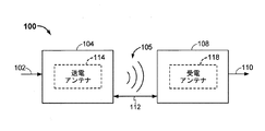
図1は、1つの例示的な実装形態によるワイヤレス電力伝達システム100の機能ブロック図である。エネルギー伝達を実行するためのワイヤレスフィールド(たとえば、磁界または電磁界)105を生成するために、入力電力102が、電源(この図に示さず)から送電器104に供給される。レシーバ108は、ワイヤレスフィールド105に結合し、出力電力110に結合されたデバイス(この図に示さず)によって蓄積または消費される出力電力110を生成する。トランスミッタ104とレシーバ108の両方は、距離112だけ引き離されている。
FIG. 1 is a functional block diagram of a wireless
レシーバ108は、トランスミッタ104によって生成されたワイヤレスフィールド105内に位置するときに電力をワイヤレスに受電してもよい。トランスミッタ104は、ワイヤレスフィールド105によってエネルギーをレシーバ108に送電するための送電アンテナまたは送電コイル114を含む。レシーバ108は、ワイヤレスフィールド105によってトランスミッタ104から送電されたエネルギーを受電するかまたは取り込むための受電アンテナまたは受電コイル118を含む。ワイヤレスフィールド105は、トランスミッタ104によって出力されたエネルギーが受電器108によって取り込まれる場合がある領域に相当する。いくつかの実装形態では、ワイヤレスフィールド105は、トランスミッタ104の「近接フィールド」に相当してもよい。近接フィールドは、最小限の電力を送電コイル114から離れる方向に放射する送電コイル114の中の電流および電荷から生じる強い反応フィールドが存在する領域に相当してもよい。近接フィールドは、送電コイル114の約1波長(または、波長の数分の一)内に存在する領域に相当してもよい。
The
例示的な一実装形態では、ワイヤレスフィールド105は磁界であってもよく、トランスミッタ104およびレシーバ108は電力を誘導的に伝達するように構成される。トランスミッタ104およびレシーバ108は、さらに相互共振関係に従って構成されてもよい。レシーバ108の共振周波数とトランスミッタ104の共振周波数が実質的に同じであるか、または極めて近いとき、トランスミッタ104とレシーバ108との間の送電損失が低減される。共振誘導結合技法により、効率の改善、および様々な距離にわたる、様々な誘導コイル構成を用いた電力伝達が可能になる場合がある。トランスミッタ104は、相互共振関係に従って構成されるとき、一実装形態では、送電コイル114の共振周波数に対応する周波数を有する時変磁界を出力する。レシーバ108がワイヤレスフィールド105内にあるとき、時変磁界は、受電コイル118の中に電流を誘導する場合がある。受電コイル118が送電コイル114の周波数において共振するように構成されているとき、エネルギーがより効率的に伝達される場合がある。受電コイル118の中で誘導される交流(AC)は、負荷(図示せず)を充電するかまたは負荷に電力を供給するために供給される場合がある直流(DC)を生成するように上述のように整流されてもよい。
In one exemplary implementation, the
図2は、例示的な一実装形態による、ワイヤレス電力伝達システム200の機能ブロック図である。システム200は、トランスミッタ204とレシーバ208とを含む。トランスミッタ204は、発振器222と、ドライバ回路224と、フィルタ/整合回路226とを含む送電回路206を含む。発振器222は、周波数制御信号223に応答して調節される所望の周波数において信号を発生させるように構成されてもよい。発振器222は、発振器信号をドライバ回路224に供給する。ドライバ回路224は、入力電圧信号(VD)225に基づいて、たとえば、送電アンテナ214の共振周波数において送電アンテナ214を駆動するように構成される。ドライバ回路224は、発振器222から方形波を受けるとともに正弦波または方形波を出力するように構成されたスイッチング増幅器であってもよい。
FIG. 2 is a functional block diagram of a wireless
フィルタおよび整合回路226は、高調波または他の不要な周波数をフィルタ除去し、トランスミッタ204のインピーダンスを送電アンテナ214のインピーダンスに整合させる。送電アンテナ214を駆動する結果として、送電アンテナ214は、ワイヤレスフィールド205を生成して、たとえば、バッテリー236を充電するのに十分なレベルで電力をワイヤレス出力してもよい。
Filter and matching
レシーバ208は、整合回路232と整流器回路234とを含む受電回路210を含む。整合回路232は、受電回路210のインピーダンスを受電アンテナ218に整合させてもよい。整流器回路234は、交流(AC)電力入力から直流(DC)電力出力を発生させてバッテリー236を充電してもよい。レシーバ208およびトランスミッタ204は、さらに、別個の通信チャネル219(たとえば、Bluetooth(登録商標)、Zigbee、セルラーなど)上で通信してもよい。レシーバ208およびトランスミッタ204は、代替的には、ワイヤレスフィールド205の特性を使用して帯域内シグナリングによって通信してもよい。
The
図3は、例示的な実装形態による、図2の送電回路206または受電回路210の一部分の概略図である。図3に示すように、送電回路または受電回路350は、アンテナ352を含む。アンテナ352はまた、「ループ」アンテナ352と呼ばれることがあり、または「ループ」アンテナ352として構成されることがある。アンテナ352はまた、「磁気」アンテナもしくは誘導コイルと本明細書で呼ばれることがあり、または「磁気」アンテナもしくは誘導コイルとして構成されることがある。「アンテナ」という用語は、一般に、別の「アンテナ」に結合するためのエネルギーをワイヤレスに出力するかまたは受電する構成要素を指す。アンテナ352は、電力をワイヤレスに出力するかまたは受電するように構成されるタイプのコイルまたはインダクタと呼ばれることもある。本明細書で使用するアンテナ352は、電力をワイヤレスに出力しならびに/あるいは受電するように構成されているタイプの「電力伝達構成要素」の一例である。アンテナ352は、空芯、またはフェライトコアなどの物理的コアを含んでもよい(この図に示さず)。
FIG. 3 is a schematic diagram of a portion of the
アンテナ352は、共振周波数において共振するように構成された共振回路の一部分を形成してもよい。ループアンテナまたは磁気アンテナ352の共振周波数は、インダクタンスおよびキャパシタンスに基づく。インダクタンスは、単にアンテナ352によって生成されるインダクタンスであってもよいが、所望の共振周波数における共振構造を生成するためにキャパシタが追加されてもよい。非制限的な例として、キャパシタ354およびキャパシタ356が送電回路または受電回路350に追加されて、所望の動作周波数において共振する共振回路を形成する。したがって、より大きい直径のアンテナの場合、共振を持続させるのに必要なキャパシタンスのサイズは、ループの直径またはインダクタンスが増大するにつれて小さくなる場合がある。他の構成要素を使用して形成される他の共振回路も考えられる。
別の非制限的な例として、キャパシタ(図示せず)は、回路350の2つの端子間に並列に配置されてもよい。送電アンテナの場合、アンテナ352の共振周波数に実質的に相当する周波数を有する信号358は、アンテナ352への入力であってもよい。
As another non-limiting example, a capacitor (not shown) may be placed in parallel between the two terminals of
図4は、本発明の例示的な実装形態による、誘導性電力伝達システムにおいて使用される場合がある送電器400の簡略機能ブロック図である。トランスミッタ400は、送電回路402と、送電回路402に動作可能に結合された送電アンテナ404とを含む。いくつかの実装形態では、送電アンテナ404は、図2を参照して上記で説明した送電アンテナ214として構成される。いくつかの実装形態では、送電アンテナ404は、コイル(たとえば、誘導コイル)であり、またはコイル(たとえば、誘導コイル)と呼ばれることがある。いくつかの実装形態では、送電アンテナ404は、パッド、テーブル、マット、ランプ、または他の静止した構成などのより大きい構造に関連する。いくつかの実装形態では、送電アンテナ404は、充電領域内に電磁界または磁界を生成するように構成される。例示的な一実装形態では、送電アンテナ404は、受電器デバイスを充電するか、または受電器デバイスに電力供給するのに十分な電力レベルで、充電領域内の受電器デバイスに電力を送電するように構成される。
FIG. 4 is a simplified functional block diagram of a
送電回路402は、いくつかの電源(図示せず)を通じて電力を受電してもよい。送電回路402は、送電アンテナ404を駆動するように構成された様々な構成要素を含んでもよい。いくつかの例示的な実装形態では、送電回路402は、本明細書で説明するレシーバデバイスの存在および構成に基づいて、ワイヤレス電力の送電を調節するように構成されてもよい。したがって、送電回路402は、ワイヤレス電力を効率的かつ安全に供給してもよい。
The
送電回路402は、コントローラ415を含む。いくつかの実装形態では、コントローラ415はマイクロコントローラまたはプロセッサであってもよい。他の実装形態では、コントローラ415は特定用途向け集積回路(ASIC)として実装されてもよい。コントローラ415は、直接的または間接的に、送電回路402の各構成要素に動作可能に接続されてもよい。コントローラ415は、送電回路402の構成要素の各々から情報を受信し、受信した情報に基づいて計算を実行するようにさらに構成されてもよい。コントローラ415は、その構成要素の動作を調整する場合がある、構成要素の各々のための制御信号を生成するように構成されてもよい。したがって、コントローラ415は、コントローラ415によって実行された計算の結果に基づいて、電力伝達を調節するように構成されてもよい。
The
送電回路402は、コントローラ415に動作可能に接続されたメモリ420をさらに含む。メモリ420は、ランダムアクセスメモリ(RAM)、電気消去可能プログラマブル読取り専用メモリ(EEPROM)、フラッシュメモリ、または不揮発性RAMを備えてもよい。メモリ420は、コントローラ415によって実行される読取り動作および書込み動作で使用するためのデータを、一時的または永続的に記憶するように構成されてもよい。たとえば、メモリ420は、コントローラ415の計算の結果として生成されたデータを記憶するように構成されてもよい。したがって、メモリ420は、コントローラ415が経時的なデータの変化に基づいて送電回路402を調整することを可能にする。
The
送電回路402は、コントローラ415に動作可能に接続された発振器412をさらに含む。いくつかの実装形態では、発振器412は、図2を参照して上記で説明した発振器222として構成される。発振器412は、ワイヤレス電力伝達の動作周波数において発振信号を生成するように構成されてもよい。いくつかの実装形態では、送電回路402は、6.78MHzのISM周波数帯域において動作するように構成される。コントローラ415は、送電段階(または、デューティサイクル)中に発振器412を選択的に使用可能にするように構成されてもよい。コントローラ415は、発振器412の周波数または位相を調節するようにさらに構成されてもよく、それによって、特にある周波数から別の周波数に遷移するときに帯域外放射が低減する場合がある。上記で説明したように、送電回路402は、ある量の充電電力を信号によって送電アンテナ404に供給するように構成されてもよく、それによって、送電アンテナ404の周りにエネルギー(たとえば、磁束)が生成される場合がある。
The
送電回路402は、コントローラ415および発振器412に動作可能に接続されたドライバ回路414をさらに含む。ドライバ回路414は、図2を参照しながら上記で説明したようなドライバ回路224として構成されてもよい。ドライバ回路414は、上記で説明したように、発振器412から受信された信号を駆動するように構成されてもよい。
送電回路402は、送電アンテナ404に動作可能に接続された低域フィルタ(LPF)416をさらに含む。低域フィルタ416は、図2を参照して上記で説明したような整合回路418のフィルタ部分として構成されてもよい。いくつかの例示的な実装形態では、低域フィルタ416は、ドライバ回路414によって生成された、電流としてのアナログ信号および電圧としてのアナログ信号を受信するとともにフィルタ処理するように構成されてもよい。いくつかの実装形態では、低域フィルタ416はアナログ信号の位相を変更してもよい。低域フィルタ416は、電流と電圧の両方について同量の位相変化を生じさせ、それらの変化を打ち消す場合がある。いくつかの実装形態では、コントローラ415は、低域フィルタ416によって生じさせられた位相変化を補償するように構成されてもよい。低域フィルタ416は、自己ジャミングを防止する場合があるレベルまで高調波放射を低減させるように構成されてもよい。例示的な他の実装形態は、他の周波数を通過させながら特定の周波数を減衰させるノッチフィルタなどの異なるフィルタトポロジーを含んでもよい。
The
送電回路402は、低域フィルタ416および送電アンテナ404に動作可能に接続された固定インピーダンス整合回路418をさらに含んでもよい。整合回路418は、図2を参照しながら上記で説明したようなフィルタおよび整合回路226の整合部分として構成されてもよい。整合回路418は、送電回路402のインピーダンスを送電アンテナ404に整合させるように構成されてもよい。例示的な他の実装形態は、送電アンテナ404への測定された出力電力やドライバ回路414のDC電流などの測定可能な送電メトリックに基づいて変更される場合がある適応インピーダンス整合を含んでもよい。
The
トランスミッタ400がトランスミッタ400またはトランスミッタ400の充電フィールド内に存在するその他の物体に関連付けることができるレシーバデバイスの所在および状態に関する情報を収集および追跡することが必要になる場合がある。したがって、送電回路402は、(本明細書ではプロセッサとも呼ばれる)コントローラ415に接続された存在検出器480、密閉型検出器460、またはこれらの組合せを含んでもよい。コントローラ415は、存在検出器480および密閉型検出器460からの存在信号に応答して、ドライバ回路414によって供給される電力量を調整してもよい。
It may be necessary for the
非限定的な例として、存在検出器480は、トランスミッタ400のカバレージエリアに挿入された充電されるべきデバイスの最初の存在を感知するために利用される運動検出器であってもよい。検出後、トランスミッタ400はオンにされてもよく、所定の方法でレシーバデバイス上のスイッチをトグルするために、デバイスによって受電された無線周波数(RF)電力が使用されてもよく、それにより、トランスミッタ400の駆動点インピーダンスへの変化が生じる。
As a non-limiting example,
別の非制限的な例として、存在検出器480は、たとえば、トランスミッタ400に関連するコイルの上方に(図11a〜図11eを参照して以下において説明する)金属プレートが存在することを検出することによって、大型の受電ユニットを検出することができる検出器であってもよい。いくつかの例示的な実施形態では、受電ユニットにおいて見える誘導電圧の範囲を限定することが望ましい場合がある。場合によっては、受電ユニットから見える広範囲の誘導電圧またはトランスミッタ400とレシーバの過結合が、送電アンテナ404の近くに存在するかあるいは送電アンテナ404の縁部のすぐ外側に存在する位相ずれフィールドによって生じる場合がある。したがって、いくつかの態様では、存在検出器480は、単独であるいは他の構成要素と連携して、大型の金属製物体が存在すると判定してもよい。検出時に、存在検出器480は、コントローラ415が、送電アンテナ404の出力、または送電アンテナ404(図示せず)の内部に配置された追加の送電アンテナの出力、または上述の関連するコイルおよび後述の関連するコイルの出力を調整することができるようにコントローラ415に信号または指示を与えてもよい。
As another non-limiting example,
非限定的な例として、密閉型検出器460(本明細書で密閉型区画検出器または密閉型空間検出器と呼ばれることもある)は、いつ筐体が閉状態または開状態にあるのかを判定するための感知スイッチなどのデバイスであってもよい。密閉された状態にある筐体の中にトランスミッタがあるとき、トランスミッタの電力レベルを高めることができる。 As a non-limiting example, an enclosed detector 460 (sometimes referred to herein as an enclosed compartment detector or an enclosed spatial detector) determines when the enclosure is closed or open. It may be a device such as a sensing switch. When the transmitter is in a sealed enclosure, the transmitter power level can be increased.
送電回路402は、ディスクリートデバイス、ディスクリート回路、および/または構成要素の一体型アセンブリをさらに備えてもよい。
The
図5は、本発明の一実装形態によるレシーバ500のブロック図である。レシーバ500は、受電回路502と、受電アンテナ504と、負荷550とを含む。レシーバ回路502は、受電された充電電力を負荷550に供給するための負荷550に電気的に結合される。レシーバ500は負荷550の外部にあるものとして示されるが、負荷550と一体化されてもよいことに留意されたい。受電アンテナ504は、受電回路502に動作可能に接続される。受電アンテナ504は、図2/図3を参照して上記で説明したような受電アンテナ218として構成されてもよい。いくつかの実装形態では、受電アンテナ504は、上記で説明したように、送電アンテナ404の共振周波数と類似の周波数において共振するか、または指定された周波数の範囲内で共振するように同調されてもよい。受電アンテナ504は、送電アンテナ404と類似の寸法を有してもよく、または負荷550の寸法に基づいて異なるサイズを有してもよい。受電アンテナ504は、上記で説明したように、送電アンテナ404(図4)によって生成された磁界に結合し、ある量の受けたエネルギーを受電回路502に供給して負荷550に電力を供給するか、または負荷550を充電するように構成されてもよい。
FIG. 5 is a block diagram of a
受電回路502は、受電アンテナ504および負荷550に動作可能に結合される。受電回路は、図2を参照して上記で説明したような受電回路210として構成されてもよい。受電回路502によって受電アンテナに与えられるインピーダンスは、受電アンテナ504のインピーダンスを(たとえば、整合回路512によって)整合させるように構成されてもよく、それによって効率が高まる場合がある。受電回路502は、受電アンテナ504から受けたエネルギーに基づいて電力を生成するように構成されてもよい。受電回路502は、生成した電力を負荷550に供給するように構成されてもよい。いくつかの実装形態では、レシーバ500は、トランスミッタ400から受けた電力の量を示す信号を、トランスミッタ400に送信するように構成されてもよい。
Power receiving circuit 502 is operably coupled to
受電回路502は、レシーバ500の処理を調整するように構成されたプロセッサシグナリングコントローラ516を含む。
The power receiving circuit 502 includes a
受電回路502は、受けたエネルギー源を、負荷550によって使用される充電電力に変換するための電力変換回路506を含む。電力変換回路506は、DC-DC変換器510に結合されたAC-DC変換器508を含む。AC-DC変換器508は、受電アンテナ504からのACをDCに整流し、DC-DC変換器510は、整流されたエネルギー信号を負荷550に適合するエネルギーポテンシャル(たとえば、電圧)に変換する。部分整流器および完全整流器、レギュレータ、ブリッジ、ダブラ、ならびにリニア変換器およびスイッチング変換器を含む、様々なAC-DC変換器が企図される。
The power receiving circuit 502 includes a
受電回路502は、受電アンテナ504を電力変換回路506に接続するように構成されたスイッチング回路512、または代替的に受電アンテナ504から電力変換回路506を切断するためのスイッチング回路512をさらに含んでもよい。電力変換回路506から受電アンテナ504を切断することにより、充電可能デバイス550の充電を中断するだけでなく、図4のトランスミッタ400から「見える」ような「負荷」も変更する。
The power receiving circuit 502 may further include a
上記で説明したワイヤレス電力回路、詳細には、受電回路502は、様々なポータブル電子デバイスの中に組み込まれることを意図される。いくつかのポータブルデバイスは、金属を含む様々な材料で作られたハウジングまたは他の部分を有することがある。 The wireless power circuit described above, and in particular the power receiving circuit 502, is intended to be incorporated into various portable electronic devices. Some portable devices may have a housing or other portion made of a variety of materials including metals.
図6は、図4の送電回路400において使用することができる送電回路600の一部分の概略図である。送電回路600は、図4のドライバ回路414に関して上記で説明したように、ドライバ回路624を含むことができる。上記で説明したように、ドライバ回路624は、方形波を受信するとともに送電回路650に供給されるべき正弦波を出力するように構成することができるスイッチング増幅器であってもよい。場合によっては、ドライバ回路624は、増幅器回路と呼ばれることがある。ドライバ回路624はE級増幅器として示されるが、任意の適切なドライバ回路624が本発明の実施形態に従って使用されてもよい。ドライバ回路624は、図4に示すような発振器412からの入力信号602によって駆動することができる。ドライバ回路624には、送電回路650を通じて供給することができる最大電力を制御するように構成された駆動電圧VDを供給することもできる。高調波を除去または低減するために、送電回路600は、フィルタ回路626を含むことができる。いくつかの実施形態では、フィルタ回路626は、3極(キャパシタ634、インダクタ632、およびキャパシタ636)の低域フィルタ回路626であってもよい。
FIG. 6 is a schematic diagram of a portion of a
フィルタ回路626によって出力された信号は、コイル614を備える送電回路650に供給することができる。送電回路650は、ドライバ回路624によって供給されるフィルタ処理済み信号の周波数で共振することができるキャパシタンス620およびインダクタンスを有する直列共振回路を含むことができる。様々な実施形態では、コイルまたは追加のキャパシタ構成要素が、インダクタンスまたはキャパシタンスを生成することができる。送電回路650の負荷は、可変抵抗器622によって表すことができる。負荷は、送電回路650から電力を受電するように位置決めされたワイヤレス電力受電器500の関数であってもよい。
The signal output by the
たとえば、図4に関して上記で説明したように、トランスミッタ400は、近くの物体の存在、距離、向き、および/またはロケーションを検出することができる存在検出器480を含むことができる。様々な他の実施形態では、存在検出器480は、たとえば、レシーバ500上、または他の場所などの別のロケーションに位置することができる。コントローラ415は、第1の位置において大きな金属シートが検出されたときに送電電力または送電フィールドパターンを変更することができる。様々な実施形態では、ワイヤレス電力伝送システム100は、本明細書において説明する実施形態に従ってワイヤレス電力伝送の特性を調整することができる。たとえば、ワイヤレス電力伝送システム100は、磁界の位相ずれ部分の作用を軽減するように送電電力を調整することができる。いくつかの態様では、この軽減は、位相ずれ部分の特性を変更することによって行われても、位相ずれ部分の少なくとも一部から受電ユニットを遮蔽することによって行われても、送電共振器の特定の領域の電力を増大させることによって行われても、あるいはそれらの組合せによって行われてもよい。
For example, as described above with respect to FIG. 4, the
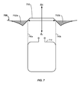
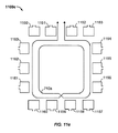
図7は、例示的な実施形態による、送電コイル710として示されたワイヤレス送電コイルの内部および周囲の様々な部分における磁界700の理論的プロットである。上述の実施形態のうちのいくつかによれば、送電コイル710は、磁界700などの、ワイヤレス電力デバイスを充電するためのフィールドを生成するように構成されてもよい。図示のように、生成された磁界700(本明細書では「Hフィールド」と呼ぶこともある)は直線部分750を含んでもよく、磁界700の強度または大きさは実質的に一様であり正である。しかし、送電コイル710の境界または周囲により近い位置では、磁界700の大きさが変動し、下向きに傾斜し始める。磁界700は、送電コイル710の縁部の実質的に上方では、ゼロ交差点740aおよび740bによって示されるように、「ゼロ交差」と呼ばれることがある。この点において、あるいは送電コイル710の周囲のすぐ外側では、磁界700はその位相を反転させる。磁界700は、その位相を反転させた後、直線部分750によって示された磁界700の位相に対して180度「ずれた」Hフィールド成分を含んでもよい。この位相ずれ成分は、逆回復領域または逆位相フィールドと呼ばれることがあり、斜線部752aおよび752bによって示されている。言い換えれば、線形領域750内の磁界成分の位相は、領域752aおよび752b内の磁界成分の位相とは異なる。
FIG. 7 is a theoretical plot of a
この位相ずれ成分は、大型の受電ユニット(PRU)、すなわち、金属裏当てを有する大型RPUに対する望ましくない影響を有する場合がある。いくつかの態様では、これらの「大型」デバイスは、タブレットサイズの形状因子を有し、たとえば、30〜60ワット範囲におけるワイヤレス電力伝達が可能なように構成されたPRUを備えてもよい。場合によっては、小型のデバイス(たとえば、全体を領域750内に配置できるほど小さいデバイス)がこの位相ずれ成分にさらなれないことがあり、あるいは場合によってはこの位相ずれ成分の影響を受けないことがある。位相ずれ成分の影響については、さらに図8を参照して説明する。 This phase shift component may have an undesirable effect on a large power receiving unit (PRU), i.e. a large RPU with a metal backing. In some aspects, these “large” devices have a tablet-sized form factor and may comprise a PRU configured to allow wireless power transfer in the 30-60 watt range, for example. In some cases, small devices (e.g., devices that are small enough to be placed entirely within region 750) may not be exposed to this phase shift component, or in some cases may not be affected by this phase shift component. is there. The influence of the phase shift component will be further described with reference to FIG.
図8は、例示的な実施形態による、図7のワイヤレス送電コイルの上方に配置されたワイヤレス電力レシーバ720を示す。図示のように、ワイヤレス電力レシーバ720は、金属裏当て735と、受電アンテナ725を備えるレシーバ回路730とを備える。レシーバ回路730は、レシーバ回路502と同様であってもよく、受電アンテナ725は、図5に関して上記において説明した受電アンテナ504と同様であってもよい。図示のように、ワイヤレス電力レシーバ720は、ワイヤレス電力レシーバ720の一部が一様なHフィールド内に(すなわち、直線部分750の上方に)あり、ワイヤレス電力レシーバ720の一部がHフィールドの位相ずれ部分(すなわち、部分752a)内にある位置に配置される。
FIG. 8 shows a
ワイヤレス電力レシーバ720がこの位置に配置されると、位相ずれ部分は金属裏当て735内に逆渦電流を誘起し、それによって、ワイヤレス電力レシーバ720における誘導電圧を著しく上昇させることができる。この場合、位相ずれ領域にさらされた金属中に生じる渦電流は受電アンテナ725において対向フィールド成分を生成し、それによって、PRUにおいて見える誘導電圧が上昇する。誘導電圧のこの上昇を送電コイル710と受電アンテナ725の「過結合」と呼ぶ場合がある。このことは、この過結合に起因してPRUの構成要素を損傷するほど高い電圧応力がPRU上に生じすることがあるので望ましくない場合がある。したがって、この場合、回路設計が困難になるかまたはコストがかかることがある。この作用は、金属裏当て735が磁界700の位相ずれ部分にさらされない位置にワイヤレス電力レシーバ720が配置されたときに結合が著しく低下することがあるので、望ましくない場合もある。この顕著な低下は、最低誘導電圧と最高誘導電圧との間の範囲が広いことを意味する場合がある。この広い範囲は、回路設計を困難にするかまたはコストを高くする場合があり、あるいはいくつかの動作制約に従わない場合がある。
When the
場合によっては、同相領域にさらされた金属中に生じた渦電流は、受電アンテナ725において対向フィールド成分を生成し、それによって、PRUにおいて見える誘導電圧が低下する。このことは、レシーバにおける電圧の低下、したがって、「結合不足」作用と呼ぶ場合がある電力結合の低下を生じさせることがあるので望ましくない場合がある。これらの作用も、回路設計を困難にするかまたはコストを高くする場合があり、レシーバをトランスミッタの中央に配置することによって悪化する場合がある。その理由は、このように配置すると、金属裏当ての最大面積が同相フィールドにさらされるからである。この場合、同相フィールドによって生じる渦電流が最大になり、レシーバにおいて電圧のずっと顕著な低下が生じることがある。
In some cases, eddy currents generated in the metal exposed to the in-phase region generate an opposing field component at the receiving
この作用を軽減するために、渦電流が低減するかまたはなくなるように金属裏当て735に不連続部を付加することができる。しかし、このことは、PRU製造業者にとって望ましくないかまたはコストがかかる場合があり、あるいは消費者にとって望ましくない場合がある。別の解決策として、位相ずれ部分にさらされる金属が少なくなるようにPRUデバイスにフェライトを付加することができる。しかし、この解決策もPRU製造業者にとって望ましくないかまたはコストがかかる場合がある。
To alleviate this effect, discontinuities can be added to the
本明細書において説明するいくつかの実施形態の態様によれば、位相ずれ部分の強度または作用を軽減させるかまたはなくすために送電コイル710に別個の構造を付加するかまたは送電コイル710の十分近くに別個の構造が配置されてもよい。これらの別個の構造については図9〜図11に関して以下において説明する。
According to aspects of some embodiments described herein, a separate structure is added to the
図9は、例示的な実施形態による、図7の送電コイル710を備える例示的なワイヤレス送電システム900の概略図である。図示のように、ワイヤレス送電システムは、「補償」コイル910によって少なくとも部分的に囲まれた送電コイル710を備える。補償コイル910は、送電コイル710の周囲の少なくとも一部を囲んでもよく、送電コイル710の周囲におけるフィールドの位相ずれ作用を軽減させるように構成されてもよい。様々な実施形態では、補償コイル910は、送電コイル710を全体的または部分的に囲む単ループコイルワイヤまたは多巻きコイルであってもよい。
FIG. 9 is a schematic diagram of an example wireless
いくつかの態様では、送電コイル710は、ループの境界の内側の内側領域と、ループの境界の外側の外側領域とを有する少なくとも1つのループを有してもよい。様々な態様では、送電コイル710は、図8のワイヤレス電力レシーバ720などのレシーバデバイスを充電するかまたはレシーバデバイスに電力を供給するための交番磁界を生成するように構成されてもよい。交番磁界は、第1の位相を有する第1の磁界成分を内側領域内に含み、第1の位相とは異なる第2の位相を有する第2の磁界成分を外側領域内に含む。一態様では、ワイヤレス送電システム900は、外側領域内にある部分を有する少なくとも1つの補償コイル910を備える。少なくとも1つの補償コイル910は、送電コイル710によって生成された第2の磁界成分を小さくするように構成されてもよい。
In some aspects, the
図示のように、補償コイル910は、補償コイル910を同調キャパシタ920に電気的に接続するコネクタ925と930を含む。いくつかの態様では、同調キャパシタ920は、補償コイル910と同調キャパシタ920とを備え、共振周波数において共振するように構成された共振回路を形成するのに使用されてもよい。共振周波数は、実質的に送電コイル710の動作周波数(たとえば、一実施形態では6.78MHz)であってもよく、あるいは動作周波数に実質的に近い他の何らかの周波数であってもよい。
As shown,
いくつかの態様では、同調キャパシタ920は存在しなくてもよく、コネクタ925および930は、補償コイル910を駆動回路(図示せず)に接続するかまたは電気的に接続してもよい。この態様によれば、駆動回路は、一次コイル駆動信号から導出される信号を用いて補償コイル910を動作可能に駆動するように構成されてもよい。この信号は、一次コイル内の電流と実質的に同様の電流を含んでもよく、あるいはこの信号を減衰させてもよい。いくつかの実装形態では、この信号は共振周波数に相当してもよい。共振周波数は、実質的に6.78MHzであってもよく、あるいは6.78MHzに近い何らかの他の周波数であってもよい。いくつかの態様では、共振周波数の変動においてある程度の公差が許容される場合がある。
In some aspects, the
一実施形態では、補償コイル910は、図4のコントローラ415などのコントローラに電気的に結合されてもよい。この実施形態によれば、コントローラは、図8のワイヤレス電力レシーバ720の受電アンテナ725などの、ワイヤレス電力デバイスの受電コイルにおける電圧を示す情報を判定するように構成されてもよい。いくつかの態様では、補償コイル910は、上述の駆動回路に電気的に結合されてもよく、この駆動回路は、コントローラまたは図4の存在検出器480などの他の何らかの検出器によって判定された情報に基づいて補償コイル910を駆動するための周波数信号を生成するように構成されてもよい。いくつかの態様では、コントローラ415は、電力レシーバ720のタイプ、送電コイル710に対する電力レシーバ720の位置、送電コイル710または補償コイル910の整流電圧、ワイヤレス電力レシーバ720の送電コイル710または受電アンテナ725に存在するインピーダンス、あるいは他の何らかの検知または判定された情報などの、他の変数に基づいて駆動信号を生成するように構成されてもよい。
In one embodiment,
補償コイル910は、送電コイル710の近くに位置してもよく、あるいは送電コイル710から遠く離れていてもよい。いくつかの態様では、補償コイル910は、z平面において送電コイル710からずれている。たとえば、送電コイル710は、第1のx-y平面を画定してもよく、補償コイル910は、第2のx-y平面において第1のx-y平面からずれていてもよい。
The
一実施形態では、補償コイル910は、補償コイル910内を流れる電流に応答して第2のフィールドを生成するように構成されてもよい。補償コイル910内を流れる電流は、電力トランスミッタコイル710によって生成されたフィールドに応答して生成されてもよい。補償コイル910内に電流を流して第2のフィールドを生成する場合がある電圧が、送電コイル710によって生成された交番磁界に基づいて誘起されてもよい。第2のフィールドは、送電コイル710に存在するかまたは送電コイル710の周囲の近くに存在する、送電コイル710によって生成されるフィールドの位相ずれ成分を低減させる(たとえば、部分的に打ち消す)ように構成されるかまたは他の方法によって使用されてもよい。位相ずれ部分を低減させることは、磁界の位相ずれ成分を小さくすることを含んでもよい。いくつかの態様では、送電コイル710によって生成されるフィールドおよび補償フィールドによって生成される第2のフィールドは磁界である。位相ずれ作用を低減させることの利点の1つの非限定的な例は、少なくとも部分的に位相ずれ領域内に位置する電力レシーバ720などのPRUにおける誘導電圧が低下し、それによってPRUに対応する電圧応力が弱くなり、PRUから見える誘導電圧の全範囲が狭くなり、PRU設計のコストが簡略化されるかまたは削減されることである。別の考えられる利益は、電力レシーバ720などのPRUにおける誘導電圧が上昇することであり、それによって、PRUに結合される電力を増大させることができる。これらの利点によって、より大型のPRUをワイヤレス電力エコシステムに導入することができる。
In one embodiment, the
図10は、例示的な実施形態による、図7の送電コイル710を備える例示的なワイヤレス送電システム1000の概略図である。図示のように、ワイヤレス送電システム1000は、遮蔽部分1010によって少なくとも部分的に囲まれた送電コイル710を備える。上述のように、送電コイル710は、図8のワイヤレス電力レシーバ720などのワイヤレス電力デバイスを充電するためのフィールドを生成するように構成されてもよい。遮蔽部分1010は、送電コイル710の周囲の少なくとも一部を囲んでもよく、送電コイル710の周囲におけるフィールドの位相ずれ作用を軽減させるように構成されてもよい。いくつかの態様では、遮蔽部分1010は、送電コイルの各部と重なり合ってもよく、送電コイル710によって形成された内側部分内に存在してもまたはその内側部分の上方に存在してもよい。様々な実施形態では、送電コイル710は、単ループコイルワイヤまたはアンテナであってもよい。いくつかの態様では、遮蔽部分1010は金属またはフェライト材料を含む。様々な態様では、フィールドは磁界を含む。
10 is a schematic diagram of an exemplary wireless
送電コイル710の周囲におけるフィールドの位相ずれ作用を低減させることは、いくつかの態様では、図8のワイヤレス電力レシーバ720などのワイヤレス電力デバイスを送電コイル710の周囲におけるフィールドの位相ずれ作用から遮蔽することを含んでもよい。いくつかの態様では、ワイヤレス電力デバイスをフィールドの位相ずれ作用から遮蔽することは、送電コイル710の周囲における位相ずれ磁界を小さくすることを含んでもよい。
Reducing field out-of-phase effects around the
一実施形態では、遮蔽部分1010は、送電コイル710の周囲を囲む連続するループの1つまたは複数の部分を含む金属部分またはフェライト部分を備え、この1つまたは複数の部分は、スペースまたはスリットによって分離される。他の実施態様では、遮蔽部分1010は、送電コイルの周囲を囲む連続するループを形成する金属部分またはフェライト部分を備える。
In one embodiment, the shielding
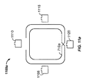
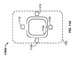
図11aは、例示的な実施形態による、送電コイル710aを備える例示的な検出システムまたは軽減システム1100aの概略図を示す。図示のように、検出システムまたは軽減システム1100aは、送電コイル710aと、送電コイル710aの外側に位置する複数のコイル1105、1110、1115、および1120とを備える。図示のように、複数のコイル1105〜1120の各々は、送電コイル710aよりもサイズが小さい。しかし、他の実施形態では、複数のコイル1105〜1120の各々は、サイズが送電コイル710a以上である。送電コイル710aは、図7の送電コイル710に類似していてもよい。様々な態様では、送電コイル710aは、ワイヤレス電力デバイスを充電するための一次フィールドを生成するように構成される。いくつかの態様では、複数のコイル1105〜1120は、送電コイル710aの周囲における一次フィールドの位相ずれ作用を低減させるように構成される。
FIG. 11a shows a schematic diagram of an exemplary detection or
一態様では、一次フィールドの位相ずれ作用を低減させることは、複数のコイル1105〜1120によって二次フィールドを生成することを含む。一実施形態では、一次フィールドの位相ずれ作用を低減させることは、(たとえば、二次フィールドを生成することによって)複数のコイル1105〜1120のうちの少なくとも1つによってPRUなどのデバイスの存在を検出したことに応答して行われてもよい。この実施形態では、デバイスの存在を検出することは、図4の存在検出器480などの構成要素から情報を収集することを含んでもよい。様々な態様では、一次フィールドと二次フィールドの各々は磁界を含む。一実施形態では、この二次フィールドは一次フィールドと同相であってもよい。一態様では、二次フィールドは一次フィールドと大きさが異なる(たとえば、より低いかまたはより高い)。フィールドが小さくなるにつれて位相ずれ成分に対向する/位相ずれ部分を打ち消す傾向がある。
In one aspect, reducing the phase shift effect of the primary field includes generating a secondary field with the plurality of coils 1105-1120. In one embodiment, reducing the phase shift effect of the primary field detects the presence of a device such as a PRU by at least one of the plurality of coils 1105-1120 (e.g., by generating a secondary field). It may be done in response to that. In this embodiment, detecting the presence of the device may include collecting information from components such as
ユーザは、PRUなどのワイヤレスデバイスを充電する際、中央に位置する送電コイル710aを備える充電パッドなどの電力トランスミッタユニット(PTU)の中心部(たとえば、概して送電コイル710aの中心の周りの領域に相当してもよい中心部)内にワイヤレスデバイスを配置する傾向がある場合がある。しかし、上述のようなより大型のPRUは、中央に配置されると適切に機能しない場合がある。たとえば、上記の説明と同様に、受電アンテナを有するPRUを送電コイルの中央に配置することは、PTUによって生成される磁界の位相ずれ部分内にPRUの一部(たとえば、PRUの本体またはPRU内の金属裏当て)を配置することを含む場合がある。位相ずれ部分内に配置されるPRUの部分は著しく大きくなる場合があり、それによって本明細書において説明する問題が深刻化することがある。
When a user charges a wireless device such as a PRU, the center of a power transmitter unit (PTU) such as a charging pad with a centrally located
一実施形態によれば、検出システムまたは軽減システム1100aは、図4のコントローラ415などのコントローラを備えてもよい。コントローラ415は、複数のコイル1105〜1120のうちの少なくとも1つの上方にデバイスが存在することを検出するように構成されてもよい。一実施形態では、デバイスが存在することの検出には、図4の存在検出器480を利用してもよい。いくつかの態様では、検出されるデバイスは、大型の金属プレートまたは裏当てを有するPRUであってもよい。これらの態様によれば、一次フィールドの位相ずれ作用を低減させることは、デバイスの存在を検出することに基づいて送電コイル710aの中央領域における一次フィールドを大きくすることを含んでもよい。送電コイルの中央領域における一次フィールドを大きくする方法は、様々な異なる方法において実施されてもよく、たとえば、送電コイル710aの内側領域内に位置する1つまたは複数の追加の送電コイルを備えてもよい。一次フィールドを大きくする方法は、追加または代替として、送電コイル710aにおける電流を増大させることを含んでもよい。非限定的な一例では、この場合、ユーザがPRUをPTUの中央に配置し、PRUのより効率的な結合を実現することが可能になる場合がある。
According to one embodiment, the detection or
図11bは、例示的な実施形態による、送電コイル710bを備える例示的な検出システムまたは軽減システム1100bの概略図を示す。図示のように、検出システムまたは軽減システム1100bは、送電コイル710bと、送電コイル710bの外側に位置する複数のコイル1125、1130、および1135とを備える。送電コイル710bは、図7の送電コイル710または図11aの送電コイル710aに類似していてもよい。しかし、図示のように、送電コイル710bは、方形形状または矩形形状ではなく、円形形状のループコイルアンテナを備える。したがって、一実施形態では、検出システムまたは軽減システム1100bは、4つのコイルではなく、送電コイル710bの周りに概ね等しい間隔を置いて配置された3つのコイル1125〜1135を含む。しかし、当業者には、設計制約およびエンドユーザの要求などの他の要求に応じて、検出システムまたは軽減システム1100aにおいて必要なコイルが3つだけである場合があることが諒解されよう。当業者には、コイルの任意の数またはそのサイズが、これらの制約および要求に基づいて異なってもよいことが了解されよう。さらに、当業者には、本明細書において開示した様々な実施形態が、図11aについて上記で議論したものなどのように、ほとんどまたはまったく修正なしに他の送電コイル形状に同様に適用されてもよいことを了解されたい。
FIG. 11b shows a schematic diagram of an exemplary detection or
図11cは、例示的な実施形態による、受電ユニット720とともに使用される別の例示的な検出システムまたは軽減システム1100cの概略図を示す。図7および図11aに関する上記の説明と同様に、ユーザは、ワイヤレス電力レシーバ720を送電コイル710aの中央からずらして配置してもよい。したがって、一実施形態では、検出システムまたは軽減システム1100cは、複数のコイル1105〜1120の各々のインピーダンスの変化を検出するように構成される場合がある図4のコントローラ415などのコントローラを備えてもよい。この検出は、複数のコイル1105〜1120のうちの少なくとも1つの上方にデバイスが存在することを検出するために利用されてもよい。いくつかの態様では、検出されるデバイスは、大型の金属プレートまたは裏当てを有するワイヤレス電力レシーバ720であってもよい。この実施形態によれば、一次フィールドの位相ずれ作用を低減させることは、インピーダンスの変化が検出される複数のコイル1105〜1120の少なくとも一部によって二次フィールドを生成することを含むことができる。たとえば、二次フィールドは、インピーダンスの変化が検出された個々の複数のコイル1105〜1120の各々においてのみ生成されてもよい。他の実施形態では、複数のコイル1105〜1120は常に二次フィールドを生成してもよく、いくつかの態様では、検出システムまたは軽減システム1100cはコントローラを備えなくてもよい。他の実施形態では、コントローラ(存在する場合)は、重なり合いを検出したコイルの数が限られており、金属裏当てに対する逆位相結合を補償する必要性が低くなったことを示す場合には、送電コイルの中央領域内の一次フィールドを大きくしなくてもよい。さらに、生成された二次フィールドは、ワイヤレス電力レシーバ720にワイヤレス電力の少なくとも一部を供給するのに使用されてもよい。
FIG. 11c shows a schematic diagram of another exemplary detection or
図11dは、例示的な実施形態による、受電ユニットとともに使用される別の例示的な検出システムまたは軽減システム1100dの概略図を示す。図示のように、検出システムまたは軽減システム1100dは、中央に位置するワイヤレス電力レシーバ720を備える。したがって、図11cの検出システムまたは軽減システム1100cと同様に、図示の複数のコイル1105〜1120のうちのすべての4つのコイルがコントローラによってアクティブ化されてもよい。一態様では、複数のコイル1105〜1120は、送電コイル710aの周囲における位相ずれフィールドの作用を低減させ、さらにワイヤレス電力レシーバ720用のワイヤレス電力充電フィールドを生成する二次フィールドを生成してもよい。他の実施形態では、コントローラ(存在する場合)は、顕著な数のコイルが重なり合いを検出し、金属裏当てに対する逆位相結合を補償する必要性が高くなったことを示す場合には、送電コイルの中央領域内の一次フィールドを大きくしてもよい。
FIG. 11d shows a schematic diagram of another example detection or mitigation system 1100d used with a power receiving unit, according to an example embodiment. As shown, the detection or mitigation system 1100d comprises a centrally located
図11eは、例示的な実施形態による、送電コイルを備える例示的な検出システムまたは軽減システム1100eの概略図を示す。図示のように、検出システムまたは軽減システム1100eは、送電コイル710aと、送電コイル710aの外側に位置する複数のコイル1150〜1163とを備える。図示のように、複数のコイル1150〜1163は送電コイル710aを実質的に囲む。当業者には、設計制約およびエンドユーザの要求などの他の要求に応じて、上記よりも少ないコイルまたは上記よりも多くのコイルが検出システムまたは軽減システム1100eにおいて使用されてもよいことが諒解されよう。非限定的な例として、コイルに送電コイル710aの周囲を囲ませる1つの利点は、送電コイル710aの位相ずれ部分を低減させることに加えて、PRUに利用可能な電力充電フィールドが拡張されてもよいことである。
FIG. 11e shows a schematic diagram of an example detection or
図12は、例示的な実施形態による、ワイヤレス電力を供給する例示的な方法1200のフローチャートである。本明細書では、図1〜図2に関して上記で説明したワイヤレス電力伝送システム100、図4に関して上記で説明したトランスミッタ400、および図9に関して上記で説明したワイヤレス送電システム900を参照しながら方法1200について説明するが、いくつかの実施形態では、方法1200は、本明細書で説明する別のデバイス、または任意の他の適切なデバイスによって実施されてもよい。いくつかの実施形態では、方法1200のブロックは、たとえば、コントローラ415(図4参照)などのプロセッサまたはコントローラによって実行されてもよい。本明細書では方法1200について特定の順序に従って説明するが、様々な実施形態では、本明細書のブロックを異なる順序で実施するかまたは省略することができ、さらなるブロックが追加されてもよい。
FIG. 12 is a flowchart of an
ブロック1205において、送電コイル(送電コイル710、710a、または710bなど)は、ワイヤレス電力デバイスを充電するためのフィールドを生成する。ブロック1210において、補償コイル(補償コイル910など)が、送電コイルの周囲におけるフィールドの位相ずれ作用を補償コイルによって低減させる。補償コイルは、送電コイルの周囲の少なくとも一部を囲む。いくつかの態様では、補償コイルは単ループのワイヤを備える。いくつかの態様では、送電コイルは、第1のx-y平面を画定し、補償コイルは、第2のx-y平面において第1のx-y平面からずれる。いくつかの態様では、フィールドは磁界を含み、位相ずれ作用は逆位相(または逆回復)フィールドである。
In
一実施形態の一態様では、補償コイルは、補償コイル内を流れる電流に応答して第2のフィールドを生成することができ、この電界は、送電コイルによって生成されたフィールドに応答して生成され、第2のフィールドは、送電コイルの周囲におけるフィールドの位相ずれ作用を低減させるように設定される。 In one aspect of an embodiment, the compensation coil can generate a second field in response to current flowing in the compensation coil, and the electric field is generated in response to the field generated by the power transmission coil. The second field is set so as to reduce the phase shift effect of the field around the power transmission coil.
いくつかの態様では、補償コイルは、共振周波数において共振してもよい。様々な態様において、このことは、同調キャパシタを補償コイルに電気的に結合して共振回路を形成することによって、部分的に実現されてもよい。いくつかの態様では、共振周波数は実質的に6.78MHzである。追加または代替として、駆動回路が、信号を用いて共振周波数において補償コイルを動作可能に駆動してもよい。いくつかの態様において、このことは、補償コイルを駆動回路に電気的に結合することによって、部分的に実現されてもよい。いくつかの態様では、共振周波数は実質的に6.78MHzである。様々な実施形態では、方法1200は、ワイヤレス電力デバイスの受電コイルにおける電圧を示す情報を判定することを含んでもよい。これらの実施形態によれば、駆動回路は、判定された情報に基づいて共振周波数を生成してもよい。
In some aspects, the compensation coil may resonate at the resonant frequency. In various aspects, this may be achieved in part by electrically coupling the tuning capacitor to the compensation coil to form a resonant circuit. In some embodiments, the resonant frequency is substantially 6.78 MHz. Additionally or alternatively, a drive circuit may operably drive the compensation coil at the resonant frequency using the signal. In some aspects, this may be achieved in part by electrically coupling the compensation coil to the drive circuit. In some embodiments, the resonant frequency is substantially 6.78 MHz. In various embodiments, the
図13は、例示的な実施形態による、ワイヤレス電力を供給する例示的な方法1300のフローチャートである。本明細書では、図1〜図2に関して上記で説明したワイヤレス電力伝送システム100、図4に関して上記で説明したトランスミッタ400、および図9に関して上記で説明したワイヤレス送電システム900を参照しながら方法1300について説明するが、いくつかの実施形態では、方法1300は、本明細書で説明する別のデバイス、または任意の他の適切なデバイスによって実施されてもよい。いくつかの実施形態では、方法1300のブロックは、たとえば、コントローラ415(図4参照)などのプロセッサまたはコントローラによって実行されてもよい。本明細書では方法1300について特定の順序に従って説明するが、様々な実施形態では、本明細書のブロックを異なる順序で実施するかまたは省略することができ、さらなるブロックを追加してもよい。
FIG. 13 is a flowchart of an
ブロック1305において、第1のコイル(送電コイル710、710a、または710bなど)を利用してワイヤレス電力デバイスを充電するかまたはワイヤレス電力デバイスに電力を供給するための第1の交番磁界を生成する。第1のコイルは、少なくとも1つのループを有し、少なくとも1つのループが、少なくとも1つのループの境界の内側に内側領域を形成し、少なくとも1つのループの境界の外側に外側領域を形成し、第1の交番磁界は、第1の位相を有する第1の磁界成分を内側領域内に有し、第1の交番磁界はさらに、第2の位相を有する第2の磁界成分を外側領域内に有し、第2の磁気位相が第1の磁気位相とは異なる、ステップを含む。
At
ブロック1310において、第2のコイル(補償コイル910など)を利用して第2の磁界成分を小さくする。第2のコイルは、一部を外側領域内に含む。一実施形態では、第2の磁界成分を小さくすることは、信号を用いて駆動回路によって第2のコイルを動作可能に駆動することを含む。関係する実施形態では、駆動回路は、信号を用いて共振周波数において第2のコイルを動作可能に駆動してもよい。一実施形態の一態様では、ワイヤレス電力デバイスの受電コイルにおける電圧を示す情報が判定されてもよい。判定された情報に基づいて、駆動回路によって第2のコイルを動作可能に駆動するための信号が生成されてもよい。いくつかの態様では、第2のコイルは単ループのワイヤを備える。いくつかの態様では、第1のコイルは、第1のx-y平面を画定し、第2のコイルは、第2のx-y平面において第1のx-y平面からずれる。様々な態様では、第2の磁界成分は逆位相(または逆回復)フィールドを含む。
In
一実施形態の一態様では、第1のコイルを備える第1の共振回路が、共振周波数において共振してもよく、第2のコイルを備える第2の共振回路が、実質的に第1の共振回路の共振周波数において共振してもよい。いくつかの態様では、共振周波数は実質的に6.78MHzである。 In one aspect of an embodiment, a first resonant circuit comprising a first coil may resonate at a resonant frequency, and a second resonant circuit comprising a second coil is substantially the first resonant You may resonate at the resonant frequency of the circuit. In some embodiments, the resonant frequency is substantially 6.78 MHz.
いくつかの態様では、第2のコイルは、第2の位相を有する第2の磁界成分を小さくするために第2の位相を有する第2の磁界成分に対向する第2の磁界を生成することができる。様々な態様では、第2の交番磁界は、第2のコイル内を流れる電流に応答して生成され、電流は、第2のコイル内で誘起された電圧に応答して流れ、電圧は、第1の交番磁界に基づいて誘起される。 In some aspects, the second coil generates a second magnetic field opposite the second magnetic field component having the second phase to reduce the second magnetic field component having the second phase. Can do. In various aspects, the second alternating magnetic field is generated in response to a current flowing in the second coil, the current flows in response to an induced voltage in the second coil, and the voltage is Induced based on an alternating magnetic field of 1.
一実施形態の一態様では、この方法は、外側領域に位置する複数のコイルによって第2の磁界成分を小さくすることを含んでもよい。一実施形態では、複数のコイルは第2のコイルを備える。一実施形態では、この方法は、ワイヤレス電力デバイスと複数のコイルの少なくとも一部の結合に基づいてワイヤレス電力デバイスの位置を判定することを含む。この実施形態によれば、第2の磁界成分を小さくするように、判定された位置に部分的に基づいて、複数のコイルのうちの1つまたは複数が選択的にアクティブ化されてもよい。 In one aspect of an embodiment, the method may include reducing the second magnetic field component by a plurality of coils located in the outer region. In one embodiment, the plurality of coils comprises a second coil. In one embodiment, the method includes determining a position of the wireless power device based on a combination of at least a portion of the wireless power device and the plurality of coils. According to this embodiment, one or more of the plurality of coils may be selectively activated based in part on the determined position so as to reduce the second magnetic field component.
図14は、例示的な実施形態による、ワイヤレス電力を供給する例示的な方法1400のフローチャートである。本明細書では、図1〜図2に関して上記で説明したワイヤレス電力伝送システム100、図4に関して上記で説明したトランスミッタ400、および図10に関して上記で説明したワイヤレス送電システム1000を参照しながら方法1400について説明するが、いくつかの実施形態では、方法1400は、本明細書で説明する別のデバイス、または任意の他の適切なデバイスによって実施されてもよい。いくつかの実施形態では、方法1400のブロックは、たとえば、コントローラ415(図4参照)などのプロセッサまたはコントローラによって実行されてもよい。本明細書では方法1400について特定の順序に従って説明するが、様々な実施形態では、本明細書のブロックを異なる順序で実施するかまたは省略することができ、さらなるブロックが追加されてもよい。
FIG. 14 is a flowchart of an
ブロック1405において、送電コイル(送電コイル710、710a、または710bなど)がワイヤレス電力デバイスを充電するかまたはワイヤレス電力デバイスに電力を供給するための第1の交番磁界を生成する。送電コイルは、少なくとも1つのループを有し、少なくとも1つのループが、少なくとも1つのループの境界の内側に内側領域を形成し、少なくとも1つのループの境界の外側に外側領域を形成し、第1の交番磁界は、第1の位相を有する第1の磁界成分を内側領域内に有し、第1の交番磁界はさらに、第2の位相を有する第2の磁界成分を外側領域内に有し、第2の磁気位相は第1の磁気位相とは異なる。ブロック1410において、金属部分またはフェライト部分(遮蔽部分1010など)がワイヤレス電力デバイスを第2の磁界成分から遮蔽する。金属部分またはフェライト部分は、送電コイルの周囲の少なくとも一部を囲む。いくつかの態様では、金属部分またはフェライト部分は、送電コイルの周囲を囲む連続するループの1つまたは複数の部分を備え、この1つまたは複数の部分は、スペースによって分離される。他の態様では、金属部分またはフェライト部分は、送電コイルの周囲を囲む連続するループを形成する。
At
様々な態様では、第2の磁界成分は逆位相(または逆回復)フィールドを含む。いくつかの態様では、ワイヤレス電力レシーバデバイスを第2の磁界成分から遮蔽することは、第2の磁界成分を小さくすることを含む。 In various aspects, the second magnetic field component includes an antiphase (or reverse recovery) field. In some aspects, shielding the wireless power receiver device from the second magnetic field component includes reducing the second magnetic field component.
図15は、例示的な実施形態による、ワイヤレス電力を供給する例示的な方法1500のフローチャートである。本明細書では、図1および図2に関して上記で説明したワイヤレス電力伝送システム100、図4に関して上記で説明したトランスミッタ400、および図11a〜図11eに関して上記で説明したワイヤレス送電システム1100a〜1100eを参照しながら方法1500について説明するが、いくつかの実施形態では、方法1500は、本明細書で説明する別のデバイス、または任意の他の適切なデバイスによって実施されてもよい。いくつかの実施形態では、方法1500のブロックは、たとえば、コントローラ415または存在検出器480(図4参照)などのプロセッサ、コントローラ、または検出器によって実行されてもよい。本明細書では方法1500について特定の順序に従って説明するが、様々な実施形態では、本明細書のブロックを異なる順序で実施するかまたは省略することができ、さらなるブロックが追加されてもよい。
FIG. 15 is a flowchart of an
ブロック1505において、送電コイル(送電コイル710、710a、または710bなど)がワイヤレス電力デバイスを充電するかまたはワイヤレス電力デバイスに電力を供給するための第1の交番磁界を生成する。送電コイルは、少なくとも1つのループを有し、少なくとも1つのループが、少なくとも1つのループの境界の内側に内側領域を形成し、少なくとも1つのループの境界の外側に外側領域を形成し、第1の交番磁界は、第1の位相を有する第1の磁界成分を内側領域内に有し、第1の交番磁界はさらに、第2の位相を有する第2の磁界成分を外側領域内に有し、第2の磁気位相は第1の磁気位相とは異なる。ブロック1510において、送電コイルの外側に位置する複数のコイル(コイル910など)は、第2の磁界成分を小さくする。いくつかの態様では、第2の磁界成分を小さくすることは、複数のコイルによって第2の交番磁界を生成することを含む。いくつかの態様では、第2の交番磁界は第1の交番磁界と同相である。いくつかの態様では、第2の交番磁界は第1の交番磁界よりも小さい。いくつかの態様では、複数のコイルの各々は、送電コイルよりもサイズが小さい。いくつかの態様では、複数のコイルは、送電コイルの周囲を実質的に囲む。様々な態様では、第2の磁界成分は逆位相(または逆回復)フィールドを含む。
At block 1505, a power transmission coil (such as
一実施形態の一態様では、方法1500は、複数のコイルのうちの少なくとも1つの上方にデバイスが存在することを検出することを含んでもよく、第2の磁界成分を小さくすることは、デバイスの存在の検出に基づいて(たとえば、送電コイルの中央領域において)第1の磁界成分を大きくすることを含んでもよい。追加または代替として、いくつかの態様では、方法1500は、複数のコイルの各々のインピーダンスの変化を検出することを含んでもよく、第2の磁界成分を小さくすることは、インピーダンスの変化が検出された複数のコイルの少なくとも一部によって第2の交番磁界を生成することを含んでもよい。
In one aspect of an embodiment, the
上記で説明した方法の様々な動作は、様々なハードウェアおよび/またはソフトウェア構成要素、回路、ならびに/あるいはモジュールなどの、動作を実行することが可能な任意の適切な手段によって実行されてもよい。概して、図に示される任意の動作は、動作を実行することが可能な対応する機能的手段によって実行されてもよい。たとえば、様々な態様において、ワイヤレス電力デバイスを充電するためのフィールド(たとえば、一次フィールド)を生成するための手段には、本明細書において説明するように、送電アンテナ404または送電コイル710、710a、または710bのうちのいずれか、あるいはそれらの機能的等価物などの送電コイルを含めてもよい。様々な態様において、(たとえば、ワイヤレス電力デバイスを充電するためのフィールドの)位相ずれ作用を低減させる手段には、本明細書において説明するように、補償コイル910、遮蔽部分1010、または複数のコイル1105〜1120、1125〜1135、もしくは1150〜1163のうちのいずれか、あるいはそれらの機能的等価物を含めてもよい。様々な実施形態において、第2のフィールドを生成するための手段には、補償コイル910または複数のコイル1105〜1120、1125〜1135、もしくは1150〜1163のうちのいずれか、あるいはそれらの機能的等価物を含めることができる。一実施形態において、共振するための手段には、同調キャパシタ920、同調キャパシタ920と補償コイル910とを備える共振回路、駆動回路414、ドライバ回路414と補償コイル910とを備える共振回路、またはそれらの機能的等価物を含めてもよい。
Various operations of the methods described above may be performed by any suitable means capable of performing the operations, such as various hardware and / or software components, circuits, and / or modules. . In general, any operations shown in the figures may be performed by corresponding functional means capable of performing the operations. For example, in various aspects, means for generating a field (e.g., primary field) for charging a wireless power device include a
いくつかの態様において、動作可能に駆動するための手段には、ドライバ回路414、ドライバ回路414と補償コイル910とを備える共振回路、またはそれらの機能的等価物を含めてもよい。一態様において、電圧を示す情報を判定するための手段には、コントローラ415、存在検出器480、密閉型検出器460、送電アンテナ404、それらの機能的等価物、またはそれらの何らかの組合せを含めてもよい。一実施形態において、判定された情報に基づいて共振周波数を生成するための手段には、コントローラ415、補償コイル910、同調キャパシタ920、送電アンテナ404、送電コイル710、710a、もしくは710b、またはそれらの機能的等価物、あるいはそれらの何らかの組合せを含めてもよい。いくつかの態様において、デバイスが存在することを検出するための手段には、コントローラ415、存在検出器480、密閉型検出器460、送電アンテナ404、それらの機能的等価物、またはそれらの組合せを含めてもよい。一実施形態において、一次フィールドを大きくするための手段には、送電アンテナ404、送電コイル710、710a、もしくは710b、送電コイル710、710a、もしくは710bのうちの1つの充電領域内(たとえば、送電コイルの内側部分内)に配置された追加のコイル(たとえば、送電コイル)、またはそれらの機能的等価物、あるいはそれらの何らかの組合せを含めてもよい。いくつかの態様において、インピーダンスの変化を検出するための手段には、コントローラ415、存在検出器480、密閉型検出器460、送電アンテナ404、それらの機能的等価物、またはそれらの組合せを含めてもよい。様々な実施形態において、第2のフィールドを生成するための手段には、コントローラ415、複数のコイル1105〜1120、1125〜1135、または1150〜1163のうちのいずれか、それらの機能的等価物、あるいはそれらの何らかの組合せを含めてもよい。
In some aspects, means for operably driving may include
様々な異なる技術および技法のうちのいずれかを使用して、情報および信号を表すことができる。たとえば、上記の説明全体にわたって参照することができるデータ、命令、コマンド、情報、信号、ビット、シンボル、およびチップは、電圧、電流、電磁波、磁場もしくは磁性粒子、光場もしくは光学粒子、またはそれらの任意の組合せによって表すことができる。 Information and signals can be represented using any of a variety of different technologies and techniques. For example, data, commands, commands, information, signals, bits, symbols, and chips that can be referred to throughout the above description are voltages, currents, electromagnetic waves, magnetic fields or magnetic particles, light fields or optical particles, or their It can be represented by any combination.
本明細書で開示する実施形態に関して説明した様々な例示的な論理ブロック、モジュール、回路、およびアルゴリズムステップは、電子ハードウェア、コンピュータソフトウェア、またはその両方の組合せとして実装することができる。ハードウェアおよびソフトウェアのこの互換性を明確に示すために、様々な例示的な構成要素、ブロック、モジュール、回路、およびステップについて、概してそれらの機能に関して上記で説明した。そのような機能がハードウェアとして実装されるか、またはソフトウェアとして実装されるかは、特定の用途および全体的なシステムに課される設計制約によって決まる。説明した機能は特定の適用例ごとに様々な方法で実装することができるが、そのような実装決定は、本発明の実施形態の範囲からの逸脱を引き起こすものと解釈されるべきではない。 The various exemplary logic blocks, modules, circuits, and algorithm steps described with respect to the embodiments disclosed herein can be implemented as electronic hardware, computer software, or a combination of both. To clearly illustrate this interchangeability of hardware and software, various illustrative components, blocks, modules, circuits, and steps have been described above generally in terms of their functionality. Whether such functionality is implemented as hardware or software depends upon the particular application and design constraints imposed on the overall system. Although the described functionality can be implemented in a variety of ways for a particular application, such implementation decisions should not be construed as causing deviations from the scope of embodiments of the invention.
本明細書で開示する実施形態に関して説明した様々な例示的なブロック、モジュール、および回路は、汎用プロセッサ、デジタル信号プロセッサ(DSP)、特定用途向け集積回路(ASIC)、フィールドプログラマブルゲートアレイ(FPGA)もしくは他のプログラマブル論理デバイス、個別ゲートもしくはトランジスタ論理、個別ハードウェア構成要素、または本明細書で説明した機能を実行するように設計されたそれらの任意の組合せによって実装または実行することができる。汎用プロセッサはマイクロプロセッサであってもよいが、代替として、プロセッサは、任意の従来のプロセッサ、コントローラ、マイクロコントローラ、またはステートマシンであってもよい。プロセッサはまた、コンピューティングデバイスの組合せ、たとえば、DSPとマイクロプロセッサとの組合せ、複数のマイクロプロセッサ、DSPコアと連携する1つもしくは複数のマイクロプロセッサ、または任意の他のそのような構成として実装することができる。 Various exemplary blocks, modules, and circuits described with respect to the embodiments disclosed herein include general purpose processors, digital signal processors (DSPs), application specific integrated circuits (ASICs), field programmable gate arrays (FPGAs). Or it may be implemented or performed by other programmable logic devices, individual gate or transistor logic, individual hardware components, or any combination thereof designed to perform the functions described herein. A general purpose processor may be a microprocessor, but in the alternative, the processor may be any conventional processor, controller, microcontroller, or state machine. The processor is also implemented as a combination of computing devices, eg, a DSP and microprocessor combination, a plurality of microprocessors, one or more microprocessors associated with a DSP core, or any other such configuration. be able to.
本明細書で開示する実施形態に関して説明した方法またはアルゴリズムおよび機能のステップは、直接ハードウェアとして具現化されてもよく、プロセッサによって実行されるソフトウェアモジュールとして具現化されてもよく、あるいはその2つの組合せとして具現化されてもよい。ソフトウェアとして実装される場合、機能は、1つまたは複数の命令またはコードとして有形の非一時的コンピュータ可読媒体上に記憶するか、あるいは有形の非一時的コンピュータ可読媒体によって送信することができる。ソフトウェアモジュールは、ランダムアクセスメモリ(RAM)、フラッシュメモリ、読取り専用メモリ(ROM)、電気的プログラマブルROM(EPROM)、電気的消去可能プログラマブルROM(EEPROM)、レジスタ、ハードディスク、リムーバブルディスク、CD ROM、または、当技術分野で知られている任意の他の形態の記憶媒体の中に存在することができる。記憶媒体は、プロセッサが記憶媒体から情報を読み取り、かつ記憶媒体に情報を書き込むことができるように、プロセッサに結合される。代替として、記憶媒体はプロセッサと一体であってもよい。本明細書で使用するディスク(disk)およびディスク(disc)は、コンパクトディスク(CD)、レーザーディスク(登録商標)、光ディスク、デジタル多用途ディスク(DVD)、フロッピーディスクおよびブルーレイディスクを含み、ディスク(disk)は通常、データを磁気的に再生し、ディスク(disc)は、レーザーを用いてデータを光学的に再生する。上記の組合せも、コンピュータ可読媒体の範囲内に同じく含まれるものとする。プロセッサおよび記憶媒体は、ASICの中に存在することができる。 The method or algorithm and functional steps described with respect to the embodiments disclosed herein may be implemented directly as hardware, may be implemented as software modules executed by a processor, or two of them. It may be embodied as a combination. If implemented as software, the functions may be stored as one or more instructions or code on a tangible non-transitory computer readable medium or transmitted by a tangible non-transitory computer readable medium. Software modules can be random access memory (RAM), flash memory, read only memory (ROM), electrically programmable ROM (EPROM), electrically erasable programmable ROM (EEPROM), registers, hard disk, removable disk, CD ROM, or It can reside in any other form of storage medium known in the art. A storage medium is coupled to the processor such that the processor can read information from, and write information to, the storage medium. In the alternative, the storage medium may be integral to the processor. Discs and discs used in this specification include compact discs (CD), laser discs (registered trademark), optical discs, digital versatile discs (DVDs), floppy discs, and Blu-ray discs. The disk normally reproduces data magnetically, and the disc optically reproduces data using a laser. Combinations of the above should also be included within the scope of computer-readable media. The processor and the storage medium can reside in an ASIC.
本明細書では、本開示を要約するために、本発明のいくつかの態様、利点、および新規の特徴について説明した。すべてのそのような利点が、本発明の任意の特定の実施形態に従って実現することができるとは限らないことを理解されたい。したがって、本発明は、本明細書で教示または示唆することができる他の利点を必ずしも実現することなく、本明細書で教示されるような1つの利点または利点のグループを実現または最適化するように具現化または実行することができる。 In this specification, several aspects, advantages, and novel features of the present invention have been described in order to summarize the present disclosure. It should be understood that not all such advantages can be realized in accordance with any particular embodiment of the invention. Accordingly, the present invention is intended to realize or optimize one advantage or group of advantages as taught herein without necessarily realizing the other advantages that may be taught or suggested herein. Can be embodied or implemented.
上記で説明した実施形態の様々な修正が容易に明らかになり、本明細書で定義される一般原理は、本発明の趣旨または範囲を逸脱することなく他の実施形態に適用することができる。したがって、本発明は、本明細書に示される実施形態に限定されることを意図しておらず、本明細書に開示する原理および新規の特徴と一致する最も広い範囲を与えられるものとする。 Various modifications to the embodiments described above will be readily apparent and the general principles defined herein may be applied to other embodiments without departing from the spirit or scope of the invention. Accordingly, the present invention is not intended to be limited to the embodiments shown herein but is to be accorded the widest scope consistent with the principles and novel features disclosed herein.
100 ワイヤレス電力伝達システム
104 トランスミッタ
105 ワイヤレスフィールド
108 レシーバ
110 出力電力
112 距離
114 送電コイル
118 受電コイル
200 ワイヤレス電力伝達システム
204 トランスミッタ
205 ワイヤレスフィールド
206 送電回路
208 レシーバ
210 受電回路
214 送電アンテナ
218 受電アンテナ
219 通信チャネル
222 発振器
223 周波数制御信号
224 ドライバ回路
226 整合回路
232 整合回路
234 整流器回路
236 バッテリー
350 受電回路
352 ループアンテナ
354 キャパシタ
356 キャパシタ
358 信号
400 トランスミッタ
402 送電回路
404 送電アンテナ
412 発振器
414 ドライバ回路
415 コントローラ
416 低域フィルタ
418 整合回路
420 メモリ
460 密閉型検出器
480 存在検出器
500 レシーバ
502 受電回路
504 受電アンテナ
506 電力変換回路
516 プロセッサシグナリングコントローラ
550 負荷
600 送電回路
602 入力信号
614 コイル
620 キャパシタンス
622 入力信号
624 ドライバ回路
626 フィルタ回路
650 送電回路
700 磁界
710 送電コイル
710a 送電コイル
710b 送電コイル
720 ワイヤレス電力レシーバ
725 受電アンテナ
735 金属裏当て
750 直線部分
752a 領域
900 ワイヤレス送電システム
910 補償コイル
920 同調キャパシタ
1000 ワイヤレス送電システム
1100a 軽減システム
1100b 軽減システム
1100c 軽減システム
1100d 軽減システム
1100e 軽減システム
1105 コイル
100 wireless power transfer system
104 transmitter
105 Wireless field
108 receiver
110 Output power
112 distance
114 Power transmission coil
118 Power receiving coil
200 wireless power transfer system
204 Transmitter
205 wireless field
206 Power transmission circuit
208 receiver
210 Power receiving circuit
214 Power transmission antenna
218 Power receiving antenna
219 communication channel
222 Oscillator
223 Frequency control signal
224 Driver circuit
226 Matching circuit
232 matching circuit
234 Rectifier circuit
236 battery
350 Power receiving circuit
352 loop antenna
354 capacitors
356 capacitors
358 signals
400 transmitter
402 Power transmission circuit
404 power transmission antenna
412 oscillator
414 Driver circuit
415 controller
416 low pass filter
418 matching circuit
420 memory
460 Sealed detector
480 Presence detector
500 receivers
502 Power receiving circuit
504 Power receiving antenna
506 Power conversion circuit
516 processor signaling controller
550 load
600 Power transmission circuit
602 Input signal
614 coil
620 capacitance
622 input signal
624 Driver circuit
626 Filter circuit
650 power transmission circuit
700 magnetic field
710 power transmission coil
710a power transmission coil
710b power transmission coil
720 wireless power receiver
725 Power receiving antenna
735 metal backing
750 straight section
752a region
900 wireless power transmission system
910 Compensation coil
920 Tuning capacitor
1000 wireless power transmission system
1100a mitigation system
1100b mitigation system
1100c mitigation system
1100d mitigation system
1100e mitigation system
1105 coil
Claims (30)
少なくとも1つのループを有する第1のコイルであって、前記少なくとも1つのループが、前記少なくとも1つのループの境界の内側に内側領域を形成し、前記少なくとも1つのループの境界の外側に外側領域を形成し、前記第1のコイルが、ワイヤレス電力デバイスを充電するかまたはワイヤレス電力デバイスに電力を供給するための第1の交番磁界を生成するように構成され、前記第1の交番磁界が、第1の位相を有する第1の磁界成分を前記内側領域内に有し、前記第1の交番磁界がさらに、第2の位相を有する第2の磁界成分を前記外側領域内に有し、前記第2の位相が前記第1の位相とは異なる第1のコイルと、
一部を前記外側領域内に含み、前記第2の磁界成分を小さくするように構成された第2のコイルとを備える、装置。 An apparatus for providing wireless power,
A first coil having at least one loop, wherein the at least one loop forms an inner region inside a boundary of the at least one loop, and an outer region outside the boundary of the at least one loop. Forming and configured to generate a first alternating magnetic field for charging or supplying power to the wireless power device, wherein the first alternating magnetic field is A first magnetic field component having a phase of 1 in the inner region; the first alternating magnetic field further having a second magnetic field component having a second phase in the outer region; A first coil having a phase of 2 different from the first phase;
A second coil comprising a portion in the outer region and configured to reduce the second magnetic field component.
前記第2のコイルを備え、実質的に前記第1の共振回路の前記共振周波数において共振するように構成された第2の共振回路とをさらに備える、請求項1に記載の装置。 A first resonant circuit comprising the first coil and configured to resonate at a resonant frequency;
2. The apparatus of claim 1, further comprising a second resonant circuit comprising the second coil and configured to resonate substantially at the resonant frequency of the first resonant circuit.
前記ワイヤレス電力デバイスと前記複数のコイルの少なくとも一部の結合に基づいて前記ワイヤレス電力デバイスの位置を判定し、
前記第2の磁界成分を小さくするように、前記判定された位置に部分的に基づいて、前記複数のコイルのうちの1つまたは複数を選択的にアクティブ化するように構成されたコントローラをさらに備える、請求項10に記載の装置。 A controller,
Determining a position of the wireless power device based on a combination of at least a portion of the wireless power device and the plurality of coils;
A controller configured to selectively activate one or more of the plurality of coils based in part on the determined position to reduce the second magnetic field component; The apparatus of claim 10, comprising:
ワイヤレス電力デバイスを充電するかまたは前記ワイヤレス電力デバイスに電力を供給するための第1の交番磁界を第1のコイルによって生成するステップであって、前記第1のコイルが、少なくとも1つのループを有し、前記少なくとも1つのループが、前記少なくとも1つのループの境界の内側に内側領域を形成し、前記少なくとも1つのループの前記境界の外側に外側領域を形成し、前記第1の交番磁界が、第1の位相を有する第1の磁界成分を前記内側領域内に有し、前記第1の交番磁界がさらに、第2の位相を有する第2の磁界成分を前記外側領域内に有し、前記第2の位相が前記第1の位相とは異なる、ステップと、
第2のコイルによって前記第2の磁界成分を小さくするステップであって、前記第2のコイルが、一部を前記外側領域内に含む、ステップとを含む、方法。 A method for supplying wireless power, comprising:
Generating a first alternating magnetic field by a first coil for charging a wireless power device or supplying power to the wireless power device, the first coil having at least one loop; The at least one loop forms an inner region inside the boundary of the at least one loop, forms an outer region outside the boundary of the at least one loop, and the first alternating magnetic field includes: A first magnetic field component having a first phase in the inner region, the first alternating magnetic field further having a second magnetic field component having a second phase in the outer region; A second phase is different from the first phase, steps;
Reducing the second magnetic field component by a second coil, wherein the second coil includes a portion in the outer region.
前記第2のコイルによって、前記第2の磁界成分に対向する第2の交番磁界を生成するステップを含む、請求項13に記載の方法。 The step of reducing the second magnetic field component includes:
14. The method of claim 13, comprising generating a second alternating magnetic field opposite to the second magnetic field component by the second coil.
前記第2のコイルを備える第2の共振回路を前記第2の共振回路によって、実質的に前記第1の共振回路の前記共振周波数において共振させるステップとをさらに含む、請求項13に記載の方法。 Resonating a first resonant circuit comprising the first coil at a resonant frequency by the first resonant circuit;
The method of claim 13, further comprising: causing a second resonant circuit comprising the second coil to resonate at the resonant frequency of the first resonant circuit with the second resonant circuit. .
前記判定された情報に基づいて、前記第2のコイルを前記駆動回路によって動作可能に駆動するための信号を生成するステップとをさらに含む、請求項19に記載の方法。 Determining information indicating a voltage at a receiving coil of the wireless power device;
20. The method of claim 19, further comprising: generating a signal for operably driving the second coil by the drive circuit based on the determined information.
ワイヤレス電力デバイスを充電するかまたはワイヤレス電力デバイスに電力を供給するための第1の交番磁界を生成するための第1の手段であって、内側領域と外側領域とを有し、前記第1の交番磁界が、第1の位相を有する第1の磁界成分を前記内側領域内に有し、第1の交番磁界がさらに、第2の位相を有する第2の磁界成分を前記外側領域内に有し、前記第2の位相が前記第1の位相とは異なる第1の手段と、
前記第2の磁界成分を小さくするための手段とを備える、装置。 A device for supplying wireless power,
A first means for generating a first alternating magnetic field for charging a wireless power device or supplying power to the wireless power device, the first means having an inner region and an outer region, the first region The alternating magnetic field has a first magnetic field component having a first phase in the inner region, and the first alternating magnetic field further has a second magnetic field component having a second phase in the outer region. And first means in which the second phase is different from the first phase;
Means for reducing the second magnetic field component.
前記第2の磁界成分に対向する第2の交番磁界を生成するための第2の手段を備える、請求項23に記載の装置。 The means for reducing the second magnetic field component is:
24. The apparatus of claim 23, comprising second means for generating a second alternating magnetic field that opposes the second magnetic field component.
実質的に前記第1の共振手段の前記共振周波数において共振するための第2の手段であって、前記小さくするための手段を備える第2の手段とをさらに備える、請求項23に記載の装置。 A first resonance means for resonating at a resonance frequency, the first resonance means comprising the first generation means;
24. The apparatus of claim 23, further comprising second means for resonating substantially at the resonant frequency of the first resonant means, the second means comprising the means for reducing. .
少なくとも1つのループを有する送電コイルであって、前記少なくとも1つのループが、前記少なくとも1つのループの境界の内側に内側領域を形成し、前記少なくとも1つのループの境界の外側に外側領域を形成し、前記送電コイルが、ワイヤレス電力デバイスを充電するかまたは前記ワイヤレス電力デバイスに電力を供給するための第1の交番磁界を生成するように構成され、前記第1の交番磁界が、第1の位相を有する第1の磁界成分を前記内側領域内に有し、前記第1の交番磁界がさらに、第2の位相を有する第2の磁界成分を前記外側領域内に有し、前記第2の位相が前記第1の位相とは異なる、送電コイルと、
前記送電コイルの周囲の少なくとも一部を囲む金属部分またはフェライト部分であって、前記ワイヤレス電力デバイスを前記第2の磁界成分から遮蔽するように構成された金属部分またはフェライト部分と備える、装置。 A device for supplying wireless power,
A power transmission coil having at least one loop, wherein the at least one loop forms an inner region inside the boundary of the at least one loop and forms an outer region outside the boundary of the at least one loop. The power transmission coil is configured to generate a first alternating magnetic field for charging or supplying power to the wireless power device, wherein the first alternating magnetic field is a first phase. A first magnetic field component having in the inner region, the first alternating magnetic field further having a second magnetic field component having a second phase in the outer region, and the second phase. Is different from the first phase, the power transmission coil,
An apparatus comprising: a metal portion or a ferrite portion surrounding at least a portion of a periphery of the power transmission coil, the metal portion or a ferrite portion configured to shield the wireless power device from the second magnetic field component.
Applications Claiming Priority (5)
| Application Number | Priority Date | Filing Date | Title |
|---|---|---|---|
| US201562156793P | 2015-05-04 | 2015-05-04 | |
| US62/156,793 | 2015-05-04 | ||
| US14/975,524 | 2015-12-18 | ||
| US14/975,524 US10033226B2 (en) | 2015-05-04 | 2015-12-18 | Methods and apparatus for out of phase field mitigation |
| PCT/US2016/026037 WO2016178769A1 (en) | 2015-05-04 | 2016-04-05 | Methods and apparatus for out of phase field mitigation |
Publications (2)
| Publication Number | Publication Date |
|---|---|
| JP2018521612A true JP2018521612A (en) | 2018-08-02 |
| JP2018521612A5 JP2018521612A5 (en) | 2019-04-25 |
Family
ID=55802469
Family Applications (1)
| Application Number | Title | Priority Date | Filing Date |
|---|---|---|---|
| JP2017557085A Pending JP2018521612A (en) | 2015-05-04 | 2016-04-05 | Method and apparatus for mitigating phase shift fields |
Country Status (5)
| Country | Link |
|---|---|
| US (1) | US10033226B2 (en) |
| EP (1) | EP3292635B1 (en) |
| JP (1) | JP2018521612A (en) |
| CN (1) | CN107534321B (en) |
| WO (1) | WO2016178769A1 (en) |
Families Citing this family (10)
| Publication number | Priority date | Publication date | Assignee | Title |
|---|---|---|---|---|
| US10224753B2 (en) | 2015-05-27 | 2019-03-05 | Qualcomm Incorporated | Wireless power transfer using a field altering circuit |
| US10516304B2 (en) | 2015-12-22 | 2019-12-24 | Intel Corporation | Wireless charging coil placement for reduced field exposure |
| US10411492B2 (en) * | 2015-12-23 | 2019-09-10 | Intel Corporation | Wireless power transmitter shield with capacitors |
| US10566850B2 (en) * | 2016-06-10 | 2020-02-18 | Witricity Corporation | Apparatus and methods for reducing magnetic field emissions between wireless power transmitters |
| US10982975B2 (en) | 2016-11-02 | 2021-04-20 | KSR IP Holdings, LLC | Duty cycle for inductive position sensors |
| EP3535547A4 (en) * | 2016-11-02 | 2020-06-10 | KSR IP Holdings LLC | Duty cycle modulation for inductive position sensors |
| DE102018103854A1 (en) * | 2018-02-21 | 2019-08-22 | Dr. Ing. H.C. F. Porsche Aktiengesellschaft | loader |
| US11482921B2 (en) * | 2019-05-03 | 2022-10-25 | Witricity Corporation | Active harmonics cancellation |
| EP4115493A4 (en) * | 2020-03-06 | 2024-04-24 | Solace Power Inc | Wireless power transfer transmitter, system and method of wirelessly transferring power |
| CN117337530A (en) * | 2021-07-02 | 2024-01-02 | Abb瑞士股份有限公司 | Coreless planar coil and power transformer |
Citations (9)
| Publication number | Priority date | Publication date | Assignee | Title |
|---|---|---|---|---|
| JP2010283777A (en) * | 2009-06-08 | 2010-12-16 | Toshiba Corp | Complex antenna, and communication device employing the same |
| US20120139356A1 (en) * | 2010-11-04 | 2012-06-07 | Hanrim Postech Co., Ltd. | Device and method for controlling wireless power signal in wireless power transmission device |
| JP2013208012A (en) * | 2012-03-29 | 2013-10-07 | Equos Research Co Ltd | Antenna coil unit and magnetic field resonance power supply system |
| US20140125275A1 (en) * | 2012-11-05 | 2014-05-08 | Qualcomm Incorporated | Systems and methods for forward link communication in wireless power systems |
| US20140246916A1 (en) * | 2013-03-01 | 2014-09-04 | Qualcomm Incorporated | Active and adaptive field cancellation for wireless power systems |
| JP2014197930A (en) * | 2013-03-29 | 2014-10-16 | 株式会社エクォス・リサーチ | Power transmission system |
| JP2014197932A (en) * | 2013-03-29 | 2014-10-16 | 株式会社エクォス・リサーチ | Power transmission system |
| JP2014197931A (en) * | 2013-03-29 | 2014-10-16 | 株式会社エクォス・リサーチ | Power transmission system |
| US20150115727A1 (en) * | 2013-10-31 | 2015-04-30 | Qualcomm Incorporated | Systems, apparatus, and method for a dual mode wireless power receiver |
Family Cites Families (4)
| Publication number | Priority date | Publication date | Assignee | Title |
|---|---|---|---|---|
| US9094057B2 (en) | 2010-08-25 | 2015-07-28 | Qualcomm Incorporated | Parasitic circuit for device protection |
| US9093215B2 (en) | 2012-05-07 | 2015-07-28 | Qualcomm Incorporated | Push-pull driver for generating a signal for wireless power transfer |
| US9697951B2 (en) * | 2012-08-29 | 2017-07-04 | General Electric Company | Contactless power transfer system |
| KR102144360B1 (en) | 2012-12-05 | 2020-08-13 | 삼성전자주식회사 | Smart nfc antenna matching network system and user device including the same |
-
2015
- 2015-12-18 US US14/975,524 patent/US10033226B2/en active Active
-
2016
- 2016-04-05 CN CN201680025966.8A patent/CN107534321B/en active Active
- 2016-04-05 JP JP2017557085A patent/JP2018521612A/en active Pending
- 2016-04-05 EP EP16717745.0A patent/EP3292635B1/en active Active
- 2016-04-05 WO PCT/US2016/026037 patent/WO2016178769A1/en active Application Filing
Patent Citations (12)
| Publication number | Priority date | Publication date | Assignee | Title |
|---|---|---|---|---|
| JP2010283777A (en) * | 2009-06-08 | 2010-12-16 | Toshiba Corp | Complex antenna, and communication device employing the same |
| US20120274521A1 (en) * | 2009-06-08 | 2012-11-01 | Kabushiki Kaisha Toshiba | Complex antenna and communication device |
| US20120139356A1 (en) * | 2010-11-04 | 2012-06-07 | Hanrim Postech Co., Ltd. | Device and method for controlling wireless power signal in wireless power transmission device |
| JP2013208012A (en) * | 2012-03-29 | 2013-10-07 | Equos Research Co Ltd | Antenna coil unit and magnetic field resonance power supply system |
| US20140125275A1 (en) * | 2012-11-05 | 2014-05-08 | Qualcomm Incorporated | Systems and methods for forward link communication in wireless power systems |
| US20140246916A1 (en) * | 2013-03-01 | 2014-09-04 | Qualcomm Incorporated | Active and adaptive field cancellation for wireless power systems |
| JP2016514447A (en) * | 2013-03-01 | 2016-05-19 | クアルコム,インコーポレイテッド | Active and adaptive field cancellation for wireless power systems |
| JP2014197930A (en) * | 2013-03-29 | 2014-10-16 | 株式会社エクォス・リサーチ | Power transmission system |
| JP2014197932A (en) * | 2013-03-29 | 2014-10-16 | 株式会社エクォス・リサーチ | Power transmission system |
| JP2014197931A (en) * | 2013-03-29 | 2014-10-16 | 株式会社エクォス・リサーチ | Power transmission system |
| US20150115727A1 (en) * | 2013-10-31 | 2015-04-30 | Qualcomm Incorporated | Systems, apparatus, and method for a dual mode wireless power receiver |
| JP2017501665A (en) * | 2013-10-31 | 2017-01-12 | クアルコム,インコーポレイテッド | System, apparatus, and method for dual-mode wireless power receiver |
Also Published As
| Publication number | Publication date |
|---|---|
| EP3292635A1 (en) | 2018-03-14 |
| CN107534321A (en) | 2018-01-02 |
| WO2016178769A1 (en) | 2016-11-10 |
| CN107534321B (en) | 2020-09-15 |
| US10033226B2 (en) | 2018-07-24 |
| US20160329748A1 (en) | 2016-11-10 |
| EP3292635B1 (en) | 2021-08-25 |
Similar Documents
| Publication | Publication Date | Title |
|---|---|---|
| JP2018521612A (en) | Method and apparatus for mitigating phase shift fields | |
| EP3189579B1 (en) | Systems and methods for adjusting magnetic field distribution using ferromagnetic material | |
| JP5921689B2 (en) | Apparatus, method, and computer readable medium for receiving wireless power using a plurality of power receiving coils | |
| EP2973939B1 (en) | Systems and methods for extending the power capability of a wireless charger | |
| JP6560247B2 (en) | System, apparatus, and method for configuration of a wireless power receiver coil | |
| KR102101528B1 (en) | Wireless power system with capacitive proximity sensing | |
| JP6401275B2 (en) | Wireless power orthogonal polarization antenna array | |
| EP2962378B1 (en) | Active and adaptive field cancellation for wireless power systems | |
| US10224753B2 (en) | Wireless power transfer using a field altering circuit | |
| JP2017524324A (en) | Wireless power transfer through metal objects | |
| WO2012109610A1 (en) | Systems and methods for calibration of a wireless power transmitter | |
| US20170063098A1 (en) | Inductive and capacitive wireless power transfer |
Legal Events
| Date | Code | Title | Description |
|---|---|---|---|
| A521 | Request for written amendment filed |
Free format text: JAPANESE INTERMEDIATE CODE: A523 Effective date: 20190313 |
|
| A621 | Written request for application examination |
Free format text: JAPANESE INTERMEDIATE CODE: A621 Effective date: 20190313 |
|
| A131 | Notification of reasons for refusal |
Free format text: JAPANESE INTERMEDIATE CODE: A131 Effective date: 20200525 |
|
| A521 | Request for written amendment filed |
Free format text: JAPANESE INTERMEDIATE CODE: A523 Effective date: 20200701 |
|
| A131 | Notification of reasons for refusal |
Free format text: JAPANESE INTERMEDIATE CODE: A131 Effective date: 20201214 |
|
| A02 | Decision of refusal |
Free format text: JAPANESE INTERMEDIATE CODE: A02 Effective date: 20210802 |