JP2018501767A - Power converter - Google Patents
Power converter Download PDFInfo
- Publication number
- JP2018501767A JP2018501767A JP2017535898A JP2017535898A JP2018501767A JP 2018501767 A JP2018501767 A JP 2018501767A JP 2017535898 A JP2017535898 A JP 2017535898A JP 2017535898 A JP2017535898 A JP 2017535898A JP 2018501767 A JP2018501767 A JP 2018501767A
- Authority
- JP
- Japan
- Prior art keywords
- conversion ratio
- scc
- voltage
- power
- power conversion
- Prior art date
- Legal status (The legal status is an assumption and is not a legal conclusion. Google has not performed a legal analysis and makes no representation as to the accuracy of the status listed.)
- Pending
Links
Images


Classifications
-
- H—ELECTRICITY
- H02—GENERATION; CONVERSION OR DISTRIBUTION OF ELECTRIC POWER
- H02M—APPARATUS FOR CONVERSION BETWEEN AC AND AC, BETWEEN AC AND DC, OR BETWEEN DC AND DC, AND FOR USE WITH MAINS OR SIMILAR POWER SUPPLY SYSTEMS; CONVERSION OF DC OR AC INPUT POWER INTO SURGE OUTPUT POWER; CONTROL OR REGULATION THEREOF
- H02M3/00—Conversion of dc power input into dc power output
- H02M3/02—Conversion of dc power input into dc power output without intermediate conversion into ac
- H02M3/04—Conversion of dc power input into dc power output without intermediate conversion into ac by static converters
- H02M3/06—Conversion of dc power input into dc power output without intermediate conversion into ac by static converters using resistors or capacitors, e.g. potential divider
- H02M3/07—Conversion of dc power input into dc power output without intermediate conversion into ac by static converters using resistors or capacitors, e.g. potential divider using capacitors charged and discharged alternately by semiconductor devices with control electrode, e.g. charge pumps
-
- H—ELECTRICITY
- H02—GENERATION; CONVERSION OR DISTRIBUTION OF ELECTRIC POWER
- H02M—APPARATUS FOR CONVERSION BETWEEN AC AND AC, BETWEEN AC AND DC, OR BETWEEN DC AND DC, AND FOR USE WITH MAINS OR SIMILAR POWER SUPPLY SYSTEMS; CONVERSION OF DC OR AC INPUT POWER INTO SURGE OUTPUT POWER; CONTROL OR REGULATION THEREOF
- H02M1/00—Details of apparatus for conversion
- H02M1/08—Circuits specially adapted for the generation of control voltages for semiconductor devices incorporated in static converters
- H02M1/088—Circuits specially adapted for the generation of control voltages for semiconductor devices incorporated in static converters for the simultaneous control of series or parallel connected semiconductor devices
-
- H—ELECTRICITY
- H05—ELECTRIC TECHNIQUES NOT OTHERWISE PROVIDED FOR
- H05B—ELECTRIC HEATING; ELECTRIC LIGHT SOURCES NOT OTHERWISE PROVIDED FOR; CIRCUIT ARRANGEMENTS FOR ELECTRIC LIGHT SOURCES, IN GENERAL
- H05B45/00—Circuit arrangements for operating light-emitting diodes [LED]
- H05B45/30—Driver circuits
- H05B45/37—Converter circuits
- H05B45/3725—Switched mode power supply [SMPS]
-
- H—ELECTRICITY
- H02—GENERATION; CONVERSION OR DISTRIBUTION OF ELECTRIC POWER
- H02M—APPARATUS FOR CONVERSION BETWEEN AC AND AC, BETWEEN AC AND DC, OR BETWEEN DC AND DC, AND FOR USE WITH MAINS OR SIMILAR POWER SUPPLY SYSTEMS; CONVERSION OF DC OR AC INPUT POWER INTO SURGE OUTPUT POWER; CONTROL OR REGULATION THEREOF
- H02M1/00—Details of apparatus for conversion
- H02M1/0048—Circuits or arrangements for reducing losses
-
- Y—GENERAL TAGGING OF NEW TECHNOLOGICAL DEVELOPMENTS; GENERAL TAGGING OF CROSS-SECTIONAL TECHNOLOGIES SPANNING OVER SEVERAL SECTIONS OF THE IPC; TECHNICAL SUBJECTS COVERED BY FORMER USPC CROSS-REFERENCE ART COLLECTIONS [XRACs] AND DIGESTS
- Y02—TECHNOLOGIES OR APPLICATIONS FOR MITIGATION OR ADAPTATION AGAINST CLIMATE CHANGE
- Y02B—CLIMATE CHANGE MITIGATION TECHNOLOGIES RELATED TO BUILDINGS, e.g. HOUSING, HOUSE APPLIANCES OR RELATED END-USER APPLICATIONS
- Y02B70/00—Technologies for an efficient end-user side electric power management and consumption
- Y02B70/10—Technologies improving the efficiency by using switched-mode power supplies [SMPS], i.e. efficient power electronics conversion e.g. power factor correction or reduction of losses in power supplies or efficient standby modes
Abstract
負荷にPWM信号を供給するための電力変換装置であって、前記電力変換装置は、前記負荷に接続されるように構成された出力を少なくとも有する誘導フィルタを備え、さらに、入力電圧を受け取り、複数の出力信号を供給するよう構成された電力変換モジュールであって、前記複数の出力信号のうちの1つが前記フィルタに供給される、電力変換モジュールと、前記電力変換モジュールに結合された変換比制御段と、前記入力電圧及び目標基準電圧に基づき、要求される変換比を決定し、前記要求される変換比に基づき、前記変換比制御段を第1の動作モード又は第2の動作モードで動作するよう制御するコントローラとを含み、前記第1の動作モードにおいて、前記電力変換モジュールは第1の変換比に従って前記出力信号を供給し、前記第2の動作モードにおいて、前記電力変換モジュールは第2の変換比に従って前記出力信号を供給する。A power converter for supplying a PWM signal to a load, the power converter comprising an inductive filter having at least an output configured to be connected to the load, further receiving an input voltage, a plurality of A power conversion module configured to supply a plurality of output signals, wherein one of the plurality of output signals is supplied to the filter, and a conversion ratio control coupled to the power conversion module And a required conversion ratio is determined based on the input voltage and the target reference voltage, and the conversion ratio control stage is operated in the first operation mode or the second operation mode based on the required conversion ratio. And in the first operating mode, the power conversion module supplies the output signal according to a first conversion ratio, and In the second mode of operation, the power converter module supplies the output signal in accordance with a second conversion ratio.
Description
本発明は、組み込み電力変換器の分野に関する。本発明は、特に、発光ダイオード(LED)光源用の駆動回路に適用することができる。より具体的には、本発明は、小型で効率的な電力変換装置に関する。 The present invention relates to the field of embedded power converters. The present invention is particularly applicable to drive circuits for light emitting diode (LED) light sources. More specifically, the present invention relates to a small and efficient power converter.
SMPS(Switched Mode Power Supplies)を使用する等、電力変換モジュールの高度な統合を要する用途は、コンデンサ及びスイッチの使用のみによって高効率のDC/DC電圧変換を提供可能なSCC(Switched Capacitor Converters)等の電力変換器に依拠することができる。 Applications that require a high degree of integration of power conversion modules, such as using SMPS (Switched Mode Power Supplies), include SCC (Switched Capacitor Converters) that can provide high-efficiency DC / DC voltage conversion only by using capacitors and switches. Reliable power converters.
特に、SSL(Solid State Lighting)業界では、小型でコンパクトなLED用電力管理ユニットの需要が増加している。LEDは、可能な限り効率的に、定電流の形態で電力供給が行われることを要する。理想的には、LED自体のサイズに匹敵するサイズのLEDドライバは、新たな照明コンセプトを実現可能にする重要なブレークスルーである。このようなソリューションは、寿命、サイズ、及び熱放散の要件に適合するために、高度な信頼性及び効率性を有するシステムを必要とする。 In particular, in the SSL (Solid State Lighting) industry, the demand for small and compact LED power management units is increasing. The LED needs to be powered in the form of a constant current as efficiently as possible. Ideally, an LED driver with a size comparable to the size of the LED itself is an important breakthrough that allows new lighting concepts to be realized. Such a solution requires a highly reliable and efficient system to meet lifetime, size, and heat dissipation requirements.
LEDドライバは、SMPSに基づき得る。SMPSはSCCを含み得るが、SCCは、高度な集積化を可能にし、高い電力変換率を達成する一方、複数の離散変換率をもたらすという欠点を有し、このため、SCCは出力電力の微調整が必要な用途に適していない。 The LED driver may be based on SMPS. Although SMPS can include SCC, SCC has the disadvantage of enabling high integration and achieving high power conversion rates while providing multiple discrete conversion rates, so SCC has a small output power. Not suitable for applications that require adjustment.
また、SMPSは、少なくとも1つのインダクタ及び少なくとも1つのスイッチを含む従来の誘導コンバータを備えてもよい。誘導コンバータは、出力電力の微調整を可能にし、任意の変換率を効率的に提供することができるが、小型の構造に容易に統合できないという欠点を有する。 The SMPS may also comprise a conventional inductive converter including at least one inductor and at least one switch. Inductive converters allow fine tuning of the output power and can efficiently provide arbitrary conversion rates, but have the disadvantage that they cannot be easily integrated into a compact structure.
H−SCC(Hybrid Switched Capacitor Converters)は、SCCの内部ノードで入手可能なパルス幅変調電圧を使用し、変換範囲を拡大し、SCCの効率を高めるために、少なくとも1つのフィルタインダクタと組み合わせられる。 H-SCC (Hybrid Switched Capacitor Converters) uses a pulse width modulation voltage available at the internal node of the SCC and is combined with at least one filter inductor to increase the conversion range and increase the efficiency of the SCC.
しかし、発明者は、H−SCCを使用すると、極端なデューティサイクルで動作させた場合に効率が大きく低下し、変換器の変換範囲が制限されることを観察した。 However, the inventors have observed that the use of H-SCC greatly reduces the efficiency when operating at extreme duty cycles and limits the conversion range of the converter.
後述する本発明の実施形態は、広範なVin/Vo比ダイナミックレンジにわたって高性能動作(高変換効率及び滑らかな出力電流(低リップル))を可能にするという利点を有する。 The embodiments of the present invention described below have the advantage of enabling high performance operation (high conversion efficiency and smooth output current (low ripple)) over a wide Vin / Vo ratio dynamic range.
本発明の一側面によれば、負荷にパルス幅変調(PWM)信号を供給するための電力変換装置であって、前記電力変換装置は、前記負荷に接続されるように構成された出力を少なくとも有する誘導出力フィルタを備え、さらに、DC入力電圧(Vin)を受け取り、出力電圧を供給するよう構成された変換比制御段と、前記出力電圧を受け取り、複数の出力信号(PWM1、・・・、PWMn)を供給するよう構成された電力変換モジュールであって、前記複数の出力信号のうちの1つが前記出力フィルタに供給される、電力変換モジュールと、前記DC入力電圧(Vin)及び目標基準電圧(Vset)に基づき、要求される変換比(m)を決定し、決定された前記要求される変換比に基づき、前記変換比制御段を第1の動作モード及び第2の動作モードのうちの1つで動作するよう制御するコントローラとを含み、前記変換比制御段が前記第1の動作モードで動作する場合、前記電力変換モジュールは第1の変換比(M1)に従って前記複数の出力信号を供給し、前記変換比制御段が前記第2の動作モードで動作する場合、前記電力変換モジュールは第2の変換比(M2)に従って前記複数の出力信号を供給する、電力変換装置が提供される。 According to one aspect of the present invention, a power converter for supplying a pulse width modulation (PWM) signal to a load, the power converter having at least an output configured to be connected to the load A conversion ratio control stage configured to receive a DC input voltage (Vin) and supply an output voltage, and to receive the output voltage, and to receive a plurality of output signals (PWM1,... A power conversion module configured to supply PWMn), wherein one of the plurality of output signals is supplied to the output filter, the DC input voltage (Vin) and the target reference voltage (Vset) is used to determine a required conversion ratio (m), and based on the determined required conversion ratio, the conversion ratio control stage is set to the first operation mode and the first operation mode. A controller that controls to operate in one of the operation modes, and wherein the conversion ratio control stage operates in the first operation mode, the power conversion module is in accordance with the first conversion ratio (M1). When the plurality of output signals are supplied and the conversion ratio control stage operates in the second operation mode, the power conversion module supplies the plurality of output signals according to a second conversion ratio (M2). A conversion device is provided.
例示的な実施形態では、前記電力変換装置は、前記DC入力電圧を供給する電圧源に接続される入力を備え、前記変換比制御段は、前記入力と前記電圧源との間に接続される。他の例示的な実施形態では、前記変換比制御段は、前記電力変換モジュール内に組み込まれる。 In an exemplary embodiment, the power converter comprises an input connected to a voltage source that supplies the DC input voltage, and the conversion ratio control stage is connected between the input and the voltage source. . In another exemplary embodiment, the conversion ratio control stage is incorporated in the power conversion module.
前記変換比制御段は複数のスイッチを備え、前記コントローラは、前記変換比制御段のスイッチ構成を制御することによって、前記変換比制御段の動作モードを制御し得る。 The conversion ratio control stage includes a plurality of switches, and the controller can control an operation mode of the conversion ratio control stage by controlling a switch configuration of the conversion ratio control stage.
前記コントローラは、さらに、前記電力変換モジュールの動作領域を決定するために、前記要求される変換比を複数の変換比閾値と比較するよう構成されてもよい。 The controller may be further configured to compare the required conversion ratio with a plurality of conversion ratio thresholds to determine an operating region of the power conversion module.
前記コントローラは、決定された前記動作領域に基づき、前記第1の動作モード及び前記第2の動作モードのうちの1つで動作するよう前記変換比制御段を制御するよう構成されてもよい。 The controller may be configured to control the conversion ratio control stage to operate in one of the first operation mode and the second operation mode based on the determined operation region.
前記コントローラは複数の比較器を含み、各比較器は、前記要求される変換比を前記複数の変換比閾値のうちの1つと比較するよう構成され得る。 The controller may include a plurality of comparators, and each comparator may be configured to compare the required conversion ratio with one of the plurality of conversion ratio thresholds.
前記コントローラは、前記目標基準電圧(Vset)を前記DC入力電圧(Vin)で割ることによって、前記要求される変換比を計算するよう構成された分圧器段を備え得る。 The controller may comprise a voltage divider stage configured to calculate the required conversion ratio by dividing the target reference voltage (Vset) by the DC input voltage (Vin).
前記電力変換装置は、選択モジュールをさらに備え、前記電力変換モジュールは、前記選択モジュールを介して前記出力フィルタに結合され、前記コントローラはさらに、前記選択モジュールを制御して、決定された前記要求される変換比に基づき、前記複数の出力信号(PWM1、・・・、PWMn)のうちの1つの出力信号を選択するよう構成され得る。あるいは、前記電力変換装置は、前記出力フィルタへの前記複数の出力信号のうちの1つの出力信号の配線をさらに備えていてもよい。 The power conversion device further comprises a selection module, the power conversion module is coupled to the output filter via the selection module, and the controller further controls the selection module to determine the requested Based on the conversion ratio, one output signal among the plurality of output signals (PWM1,..., PWMn) may be selected. Alternatively, the power conversion device may further include wiring of one output signal among the plurality of output signals to the output filter.
一実施形態では、前記第1の変換比は1/nであり(nは2以上の整数値)、前記第2の変換比は1/(n−0.5)である。他の実施形態では、前記第1の変換比は1/nであり(nは2以上の整数値)、前記第2の変換比は1/(n−1)である。 In one embodiment, the first conversion ratio is 1 / n (n is an integer value of 2 or more), and the second conversion ratio is 1 / (n−0.5). In another embodiment, the first conversion ratio is 1 / n (n is an integer value of 2 or more), and the second conversion ratio is 1 / (n−1).
例示的な実施形態では、前記複数の出力信号は、入力電圧(Vin)レベルの分数であるレベル振幅を有し、各出力信号は、フローティングであり、決定された最低分数レベル振幅から決定された最高分数レベル振幅にわたる複数のステップに分割されるバイアス成分を有する。 In an exemplary embodiment, the plurality of output signals have a level amplitude that is a fraction of the input voltage (Vin) level, each output signal being floating and determined from the determined minimum fractional level amplitude. It has a bias component that is divided into steps over the highest fractional level amplitude.
前記電力変換モジュールは、前記コントローラによって制御される複数のスイッチを含むSCC(Switched Capacitor Converter)を備えることができる。 The power conversion module may include an SCC (Switched Capacitor Converter) including a plurality of switches controlled by the controller.
前記電力変換モジュールは、第1のスイッチのセットと第2のスイッチのセットとを備えるディクソン・ラダー・トポロジーに基づき得る。 The power conversion module may be based on a Dixon ladder topology comprising a first set of switches and a second set of switches.
例示的な実施形態では、前記複数の出力信号(PWM1、・・・、PWMn)は、前記電力変換モジュールの各内部ノード(N1、・・・、N4、SN1)における電圧(vx1、・・・、vxn)によって形成される。 In an exemplary embodiment, the plurality of output signals (PWM1,..., PWMn) are voltage (vx1,...) At each internal node (N1,..., N4, SN1) of the power conversion module. , Vxn).
本発明の一側面によれば、少なくとも1つの光源と、前記少なくとも1つの光源にパルス幅変調(PWM)信号を供給するための電力変換装置とを含む照明モジュールであって、前記電力変換装置は、前記少なくとも1つの光源に接続されるように構成された出力を少なくとも有する誘導出力フィルタと、前記出力電圧を受け取り、複数の出力信号(PWM1、・・・、PWMn)を供給するよう構成された電力変換モジュールであって、前記複数の出力信号のうちの1つが前記出力フィルタに供給される、電力変換モジュールと、前記電力変換モジュールに結合された変換比制御段と、前記DC入力電圧(Vin)及び目標基準電圧(Vset)に基づき、要求される変換比(m)を決定し、決定された前記要求される変換比に基づき、前記変換比制御段を第1の動作モード及び第2の動作モードのうちの1つで動作するよう制御するコントローラとを含み、前記変換比制御段が前記第1の動作モードで動作する場合、前記電力変換モジュールは第1の変換比(M1)に従って前記複数の出力信号を供給し、前記変換比制御段が前記第2の動作モードで動作する場合、前記電力変換モジュールは第2の変換比(M2)に従って前記複数の出力信号を供給する、照明モジュールが提供される。 According to one aspect of the present invention, an illumination module includes at least one light source and a power conversion device for supplying a pulse width modulation (PWM) signal to the at least one light source, the power conversion device comprising: An inductive output filter having at least an output configured to be connected to the at least one light source; and configured to receive the output voltage and provide a plurality of output signals (PWM1,..., PWMn). A power conversion module, wherein one of the plurality of output signals is supplied to the output filter, a conversion ratio control stage coupled to the power conversion module, and the DC input voltage (Vin) ) And the target reference voltage (Vset), a required conversion ratio (m) is determined, and based on the determined required conversion ratio, A controller for controlling the conversion ratio control stage to operate in one of a first operation mode and a second operation mode, wherein the conversion ratio control stage operates in the first operation mode, When the power conversion module supplies the plurality of output signals according to a first conversion ratio (M1) and the conversion ratio control stage operates in the second operation mode, the power conversion module detects the second conversion ratio ( An illumination module is provided that provides the plurality of output signals according to M2).
上記及び他の側面は、以下に記載される実施形態から明らかになるであろう。本開示の範囲は、この概要によって限定されるものではなく、また、記載される欠点のいずれか又は全てを必ず解決する実装形態にも限定されない。 These and other aspects will become apparent from the embodiments described below. The scope of the present disclosure is not limited by this summary, nor is it limited to implementations that necessarily solve any or all of the disadvantages described.
本開示をより良く理解し、実施形態がどのように実施され得るかを示すために、以下の添付図面を参照する。 For a better understanding of the present disclosure and to show how embodiments may be implemented, reference is made to the following accompanying drawings.
LEDドライバ電力変換器の基本的要件は、例えば入力又は出力電圧、変換比、効率等の様々な電気的仕様をカバーすることができる複数のモードで動作可能なことである。 The basic requirement of an LED driver power converter is that it can operate in multiple modes that can cover various electrical specifications such as input or output voltage, conversion ratio, efficiency, etc.
SCCは、入力電圧をステップアップ又はステップダウンすることによって、調整された出力電圧を生成し得る。 The SCC may generate a regulated output voltage by stepping up or down the input voltage.
SCCの効率ηは、スイッチ抵抗に依存しない電圧伝達比の関数として表すことができる。
![]()
![]()
マルチモード電力変換器は、望ましくない動作条件によって分離された複数の所望の動作条件を有し得る。特に、マルチモード電力変換器は、負荷によって要求される電圧が範囲Vo1又は範囲Vo2のいずれかにある場合に、変換器の少なくとも1つの出力に結合された少なくとも1つの負荷に所望の態様で電力を供給可能であり、ここで、
Va>Vo1>Vb
Vc>Vo2>Vd
Vc>Vbである。
したがって、負荷が要求する電圧が範囲Vo3にあり、
Vb<Vo3<Vc
の場合、変換器は全く動作しないか、又は非常に限られた性能でしか動作しないおそれがある。
A multimode power converter may have multiple desired operating conditions separated by undesirable operating conditions. In particular, the multi-mode power converter is desirable for at least one load coupled to at least one output of the converter when the voltage required by the load is in either the range V o1 or the range V o2. Power can be supplied at, where
V a > V o1 > V b
V c > V o2 > V d
V c > V b .
Therefore, the voltage required by the load is in the range V o3 ,
V b <V o3 <V c
In this case, the converter may not work at all or may only work with very limited performance.
これらの電圧「ギャップ」は、SCCの効率を急激に低下させ、ゼロにさえ低下させ得る。 These voltage “gaps” can drastically reduce the efficiency of the SCC and even reduce it to zero.
図1は、10:1分圧器として動作する場合のH−SCC(Hybrid Switched Capacitor Converter)の効率対変換比の曲線102を示す(すなわち、10個の変換比範囲を提供可能な10個の動作領域が割り当てられており、これは、電力変換器を電圧範囲が広い用途に適用することを可能にする)。各動作領域において、変換比はデューティサイクルに比例するので、所望の変換比を達成するための一般的な方法は、例えばパルス幅変調(PWM)を使用してデューティサイクルを調整することである。
FIG. 1 shows the efficiency-to-
H−SCCを使用する場合、SCC段(ステージ)によって提供される異なる電圧範囲間の境界において、変換比は制限される。境界領域では、SCC段は、典型的には10%未満又は90%超の極端なデューティサイクルで動作する。これにより、SCC段の等価出力インピーダンスが大幅に増加し、変換器の効率が急激に低下するので、これらの境界では電力変換器は非常に限られた性能しか発揮することができない。これらの効率「ギャップ」又は「ノッチ」は図1に示され、本発明の実施形態によって対処される。 When using H-SCC, the conversion ratio is limited at the boundary between the different voltage ranges provided by the SCC stage. In the boundary region, the SCC stage operates with extreme duty cycles typically less than 10% or greater than 90%. This significantly increases the equivalent output impedance of the SCC stage and drastically reduces the efficiency of the converter, so that the power converter can only exhibit very limited performance at these boundaries. These efficiency “gaps” or “notches” are illustrated in FIG. 1 and are addressed by embodiments of the present invention.
図1は、10:1分圧器として動作する場合のH−SCC(Hybrid Switched Capacitor Converter)に関する効率「ギャップ」を示すが、 当業者は、H−SCC(Hybrid Switched Capacitor Converter)が異なる変換比を提供する場合にもこれらの効率「ギャップ」が観察されることを理解するであろう。例えば、H−SCC(Hybrid Switched Capacitor Converter)が5:1分圧器として動作する場合(すなわち、5個の変換比範囲を提供可能な5個の動作領域が割り当てられている)、異なる電圧範囲間の境界において、上述の変換器の効率低下が観察される。 Although FIG. 1 shows the efficiency “gap” for H-SCC (Hybrid Switched Capacitor Converter) when operating as a 10: 1 voltage divider, those skilled in the art will know that H-SCC (Hybrid Switched Capacitor Converter) has different conversion ratios It will be appreciated that these efficiency “gaps” are also observed when provided. For example, when an H-SCC (Hybrid Switched Capacitor Converter) operates as a 5: 1 voltage divider (ie, five operating regions capable of providing five conversion ratio ranges are allocated), between different voltage ranges At the boundary, a reduction in the efficiency of the converter described above is observed.
本開示の実施形態は、H−SCCの変換比を制御するよう構成された変換比制御段の制御によって、上述の効率「ギャップ」に対処することに関する。 Embodiments of the present disclosure relate to addressing the efficiency “gap” described above by control of a conversion ratio control stage configured to control the conversion ratio of H-SCC.
実施形態では、変換比制御段はH−SCCに結合され、特に、変換比制御段はH−SCCのSCC段に結合される。 In an embodiment, the conversion ratio control stage is coupled to the H-SCC, and in particular, the conversion ratio control stage is coupled to the SCC stage of the H-SCC.
変換比制御段204は、様々な態様でH−SCC206に結合され得る。変換比制御段204は、図2aに示されるように主電力段(H−SCC)の前の電力線入力に配置されてもよいし、図2bに示されるように主電力段内に組み込まれてもよい。
Conversion
まず、図2aに示される構成に関して実施形態を説明する。 First, an embodiment will be described with respect to the configuration shown in FIG.
図2aに示される構成に係る電力変換装置200を示す図2cを参照する。電力変換装置200は、以下Vinと表される直流電圧を供給する電圧源202に接続するための入力、及び例えば抵抗性負荷又は発光装置であり得る負荷214を有する。発光装置は1つ以上の光源、例えば単一のLED又はLEDのセット、例えばLED列を含み得る。本明細書ではLED光源を参照しているが、電力変換装置200は任意の適切な光源を駆動し、例えば有機発光ダイオード(OLED)又はレーザダイオード等を駆動してもよい。
Reference is made to FIG. 2c showing a
電力変換装置200は、変換比制御段204、H−SCC206、及びコントローラ216を備える。
The
H−SCC206は、PWM電圧を供給する複数の出力PWM1、PWM2、・・・PWMnを有するSCC段208を備える(電力変換モジュールとも呼ぶ)。本発明によれば、選択モジュールのような適切な選択手段によって複数の出力PWM1、PWM2、・・・PWMnのうちの1つが選択され、例えば出力フィルタ212を介して出力に接続され得る。例えば、複数の出力PWM1、PWM2、・・・PWMnは、マルチプレクサ210((選択モジュールとも呼ぶ)の対応する複数の入力に接続され得る。以下でさらに詳細に説明するように、マルチプレクサ210は、上記複数の入力から1つのPWM電圧PWMxを出力に送り得る。したがって、マルチプレクサ210は、n:1マルチプレクサであり得る。H−SCC206は、以下に説明する図示の例示的な実施形態のように、必ずしもマルチプレクサを備える必要はないことを理解されたい。選択モジュールは、例えば、出力PWM1、PWM2、・・・PWMnのうちの1つを出力フィルタ212を介して出力に適切に配線することによって形成することができる。
The H-
マルチプレクサ210の出力は、出力フィルタ212に接続されている。出力フィルタ212は、特に、少なくとも1つのキャパシタ又は1つのインダクタを含み得る。
The output of the
コントローラ216は、電源202によって供給される検出された電圧を表す入力信号、H−SCC206の直流出力電圧(以下、vdcと表す)、及び/又は検出された負荷電圧、負荷電流、若しくは負荷電力、例えば負荷電圧(以下、voと表す)を表す信号に基づきSCC段208及びマルチプレクサ210を制御することによって制御ループを可能にする。
The
コントローラ216は、電源202によって供給される電圧を第1の入力220として受け取る。また、コントローラ216は、H−SCC206の直流出力電圧を第2の入力228として受け取る。
The
コントローラ216の第1の出力222は、アナログ制御によってSCC段208のデューティサイクルを制御することによってSCC段208の制御を可能にする。
The
コントローラ216の第2の出力224は、マルチプレクサ210のマルチプレクサチャネルの制御を可能にする。
The
図2cに示すように、変換比制御段204は、H−SCCの前の電力線入力に配置される。以下に説明する実施形態では、変換比制御段204は、ハーフポイントSCC204を使用して実装される。コントローラ216の第3の出力226は、以下に詳述されるハーフポイントSCC204の制御を可能にする。
As shown in FIG. 2c, the conversion
ここで、本発明の例示的実施形態において、ハーフポイントSCC204及びH−SCC206をより詳細に示す電気図を示す図3を参照する。
Reference is now made to FIG. 3, which shows an electrical diagram showing the half-
ハーフポイントSCC204は、4つのスイッチSx1、Sx2、Sx3、及びSx4、並びに単一のキャパシタChpを備える。ハーフポイントSCC204は、4つのスイッチ構成のうちの1つに従って制御することができる。本明細書において、変換比制御段204のスイッチ構成とは、変換比制御段のスイッチの開閉シーケンスを指す。例えば、ハーフポイントSCC204のスイッチ構成は、スイッチSx1〜Sx4の開閉シーケンスを指すために使用される。
The
第1のスイッチ構成では、第1の時間フェーズΦ1の間はスイッチSx1、Sx2、Sx3、及びSx4の全てがオフにされ、第2の時間フェーズΦ2の間はスイッチSx1及びSx3がオンにされ、スイッチSx2及びSx4はオフにされる。すなわち、第2の時間フェーズΦ2の間、電圧VinがH−SCC206の第1の中央ノードN1に供給される。
In the first switch configuration, all of the switches Sx1, Sx2, Sx3, and Sx4 are turned off during the first time phase Φ1, and the switches Sx1 and Sx3 are turned on during the second time phase Φ2. Switches Sx2 and Sx4 are turned off. That is, during the second
第2のスイッチ構成では、第1の時間フェーズΦ1の間はスイッチSx1、Sx2、Sx3、及びSx4の全てがオフにされ、第2の時間フェーズΦ2の間はスイッチSx2及びSx4がオンにされ、スイッチSx1及びSx3はオフにされる。すなわち、第2の時間フェーズΦ2の間、電圧VinがH−SCC206の第1の中央ノードN1に供給される。
In the second switch configuration, all of the switches Sx1, Sx2, Sx3, and Sx4 are turned off during the first time phase Φ1, and the switches Sx2 and Sx4 are turned on during the second time phase Φ2. Switches Sx1 and Sx3 are turned off. That is, during the second
第3のスイッチ構成では、第1の時間フェーズΦ1の間はスイッチSx1及びSx4がオンにされる一方、スイッチSx2及びSx3がオフにされ、第2の時間フェーズΦ2の間はスイッチSx1及びSx4がオフにされる一方、スイッチSx2及びSx3がオンにされる。 In the third switch configuration, the switches Sx1 and Sx4 are turned on during the first time phase Φ1, while the switches Sx2 and Sx3 are turned off, and the switches Sx1 and Sx4 are turned on during the second time phase Φ2. While turned off, switches Sx2 and Sx3 are turned on.
第4のスイッチ構成では、第1の時間フェーズΦ1の間はスイッチSx1及びSx4がオフにされる一方、スイッチSx2及びSx3がオンにされ、第2の時間フェーズΦ2の間はスイッチSx1及びSx4がオンにされる一方、スイッチSx2及びSx3がオフにされる。 In the fourth switch configuration, the switches Sx1 and Sx4 are turned off during the first time phase Φ1, while the switches Sx2 and Sx3 are turned on and the switches Sx1 and Sx4 are turned on during the second time phase Φ2. While turned on, switches Sx2 and Sx3 are turned off.
SCC段208は、上述のように、入力直流電圧Vinの分数であるレベル振幅を有する複数のPWM出力信号を供給するように構成されている。この例示的実施形態では、PWM出力信号は、入力直流電圧Vinの分数である振幅を有する方形波電圧である。各方形波電圧はフローティングでバイアス成分を有し、非限定的な図示の例示的実施形態では、バイアス成分は最低分数振幅から最高分数振幅にかけて複数のステップに等分される。マルチプレクサ210は任意の電圧を選択し、マルチプレクサ210の出力を介して出力することができる。マルチプレクサ210の出力は出力フィルタ212に接続されているため、負荷214に連続電圧を供給することができる。
As described above, the
図3に示す非限定的な例示的実施形態では、H−SCC206は、複数のスイッチ及び複数のコンデンサを含むSCC段によって形成される。例えば、SCC段208は、いわゆるディクソンラダー変換器を含む。他のSCCトポロジー、例えば標準的なラダー、フィボナッチ、又は直列−並列等のトポロジーを使用することもできる。
In the non-limiting exemplary embodiment shown in FIG. 3, the H-
より具体的には、図示の例示的実施形態は、5つのコンデンサC1〜C5及び単極単投の8つのスイッチS1〜S8に基づくディクソンラダートポロジーを使用する。より具体的には、SCC段208は2つのフライングラダー、すなわち、直列に配置された4つのコンデンサC3及びC5を含む第1のフライングラダーと、直列に配置された2つのコンデンサC2及びC4を含む第2のフライングラダーを含む。
More specifically, the illustrated exemplary embodiment uses a Dixon ladder topology based on five capacitors C1-C5 and eight single-pole single-throw switches S1-S8. More specifically, the
SCC段208は、6つの中央ノードN1〜N6をさらに含む。第1の中央ノードN1は、ハーフポイントSCC204の電圧出力を受け取る。第1のスイッチS1は、第1の中央ノードN1を第2の中央ノードN2に選択的に接続する。第2のスイッチS2は、第2の中央ノードN2を第3の中央ノードN3に選択的に接続する。第3のスイッチS3は、第3の中央ノードN3を第4の中央ノードN4に選択的に接続する。第4のスイッチS4は、第4の中央ノードN4を第5の中央ノードN5に選択的に接続する。第1のコンデンサC1は、第5の中央ノードN5と第6の中央ノードN6との間に配置され、第6の中央ノードN6は基準電圧、例えばグランドに接続される。
コンデンサC3及びC5を含む第1のフライングラダーは、第1の中央ノードN1と第1のセカンダリノードSN1との間に配置される。第5のスイッチS5は、第1のセカンダリノードSN1を第6の中央ノードN6に選択的に接続し、第6のスイッチS6は、第1のセカンダリノードSN1を第5の中央ノードN5に選択的に接続する。 The first flyer grader including the capacitors C3 and C5 is arranged between the first central node N1 and the first secondary node SN1. The fifth switch S5 selectively connects the first secondary node SN1 to the sixth central node N6, and the sixth switch S6 selectively selects the first secondary node SN1 to the fifth central node N5. Connect to.
コンデンサC2及びC4を含む第2のフライングラダーは、第2の中央ノードN2と第2のセカンダリノードSN2との間に配置される。第7のスイッチS7は、第2のセカンダリノードSN2を第5の中央ノードN5に選択的に接続し、第8のスイッチS8は、第2のセカンダリノードSN2を第6の中央ノードN6に選択的に接続する。 The second flyer grader including the capacitors C2 and C4 is disposed between the second central node N2 and the second secondary node SN2. The seventh switch S7 selectively connects the second secondary node SN2 to the fifth central node N5, and the eighth switch S8 selectively selects the second secondary node SN2 to the sixth central node N6. Connect to.
2つのフライングラダーは、スイッチS1〜S8の適切な開閉シーケンスにより、反対の位相を有する。例えば、第1の時間フェーズΦ1の間、全ての奇数番号のスイッチS1、S3、・・・、S7は所与の状態、例えばオンにされ、後続する第2の時相フェーズΦ2の間、全ての偶数番号のスイッチS2、S4、・・・、S8は反対の状態、例えばオフにされ、全スイッチの状態が反転されてもよい。コントローラ216は、上述したように、第1の時間フェーズΦ1及び第2の時間フェーズΦ2においてスイッチS1〜S8を制御する(すなわち、SCC段208のスイッチ構成を制御する)ためのPWM信号を生成するよう構成される。
The two flyer graders have opposite phases due to the proper opening and closing sequence of the switches S1 to S8. For example, during the first time phase Φ1, all odd numbered switches S1, S3,..., S7 are all turned on in a given state, for example during the subsequent second time phase phase Φ2. The even-numbered switches S2, S4,..., S8 may be in the opposite state, eg, turned off, and the state of all the switches may be inverted. As described above, the
複数の中央ノードN1〜N4から供給された信号は、SCC段208の同数の出力を形成し、図示の実施形態では図3において電圧vx1〜vx4と表されている、H−SCC206を形成するSCCの複数の内部ノードは、マルチプレクサ210の同数の入力に接続される。したがって、この例示的な実施形態では、マルチプレクサ210は、4つの入力のうちの1つを出力vxに選択的に接続することを可能にする4つのスイッチ、及び、出力フィルタ212に印可される電圧レベルの一層改良された規定又はダイナミッスのために第1のセカンダリノードSN1に接続された追加スイッチを含む。マルチプレクサ210の構造は、負荷動作に関する要件に応じて、スイッチの数を減らすことによって簡略化することができる。
The signals supplied from the plurality of central nodes N1-N4 form the same number of outputs of the
上記したように、マルチプレクサ212は、選択モジュールの実装の一例である。H−SCC206のより簡単なアーキテクチャは、電力変換モジュールの複数の出力PWM1、PWM2、・・・PWMnの中から選択された出力の適切な配線を提供することによって実現することができ、これは、一部の用途に係る負荷の動作要件を満たし得る。そのような場合、選択モジュールは、上記適切な配線によって形成される。そのような実施形態は、特に、例えば製造工程における簡単な追加の配線ステップによって、所与の負荷に適合させることができるコスト効率が良くコンパクトなアーキテクチャを依然として提供するという利点をもたらす。
As described above, the
さらに、図3に示す例示的な実施形態では、上記ではvdcと表されるSCC段208のDC出力電圧は第1のコンデンサC1の両端の電圧、すなわち、第5の中央ノードN5と第6の中央ノードN6との間の電圧である。
Further, in the exemplary embodiment shown in FIG. 3, the DC output voltage of the
図3に示す例示的な実施形態のように、出力フィルタ212は、フィルタインダクタンスLo及びフィルタキャパシタCoを含み得る。フィルタインダクタンスLoは、マルチプレクサ210の出力と負荷214との間に、フィルタキャパシタCoに対して並列に接続される。
As in the exemplary embodiment shown in FIG. 3, the
したがって、本発明の更なる利点は、マルチプレクサ210の出力における電圧vx信号のリップルが大きく低下することであり、これは、バルクに関してフィルタインダクタンスLoの要件を緩和することを可能にし、例えばLEDモジュールによって形成される負荷214自体のサイズと同様のサイズを有する小さなパッケージに容易にインダクタンスLoを組み込むことができる。通常、インダクタンス値は電圧リップルに正比例する。したがって、電圧リップルが係数Nだけ減少すると、インダクタの大きさは同じ係数Nだけ減少し得る。
Thus, a further advantage of the present invention is that the ripple of the voltage vx signal at the output of the
このような小さなリップルは、電磁放射を減少させ、もって電磁干渉(EMI)を改善するという利点ももたらす。さらに、電力変換装置に含まれる複数のスイッチにおける電圧ストレス及び電流ストレスを大きく低減し、電力変換装置の寿命を著しく改善するという利点も提供される。 Such small ripple also has the advantage of reducing electromagnetic radiation and thus improving electromagnetic interference (EMI). Furthermore, the advantage of significantly reducing the voltage stress and current stress in the plurality of switches included in the power converter and significantly improving the life of the power converter is also provided.
本開示の実施形態によれば、H−電力変換装置200の動作は、ハーフポイントSCC204のスイッチ構成に依存して制御される。
According to the embodiment of the present disclosure, the operation of the H-
すなわち、電力変換装置200の変換比は、以下の表1に示すように、ハーフポイントSCC204のスイッチ構成を制御することによって構成することができる。

表1に示されるように、ハーフポイントSCC204が第1の動作モードで動作する場合(上述の第1又は第2のスイッチ構成のいずれかに従って、すなわちオフにされる)、電力変換装置200は、5:1分圧器、すなわち、5分割分圧器(第1の変換比M1(1/5)を有する)として動作する。ハーフポイントSCC204が第2の動作モードで動作する場合(上述の第3又は第4のスイッチ構成のいずれかに従って、すなわちオンにされる)、電力変換装置200の変換比は0.5だけ低減され、この場合、電力変換装置200は4.5:1分圧器、すなわち、4.5分割分圧器(第2の変換比M2(1/4.5)を有する)として動作する。
As shown in Table 1, when the half-
ハーフ・ポイントSCC204が第3又は第4のスイッチ構成に従って構成される場合、キャパシタChpがSCCトポロジに含まれる。一方のフェーズの間、キャパシタChpは入力電源Vinと中央ノードN1との間に接続され、他方のフェーズの間、キャパシタChpはVinと中央ノードN1との間に逆極性で接続される。当業者には明らかなように、これにより、電力変換装置200はその変換比を半ステップだけ変化させる。
If the
5:1分圧器として動作する場合、SCC段208の出力電圧は以下の通りである。
4.5:1分圧器として動作する場合、SCC段208の出力電圧は以下の通りである。
コントローラ216は、負荷電圧又は出力電流を制御するために、出力電圧Vo、及び電圧源202によって供給される入力電圧Vinに応じて、ある変換比mを提供するように構成され、ここで、m=Vo/Vinである。コントローラ216は、(i)コントローラ216の第1の出力を使用して(制御スイッチS1〜S8を制御する)PWM信号のデューティサイクルを制御することによって、(ii)コントローラ216の第2の出力を使用してマルチプレクサ210のマルチプレクサチャネルを制御することによって、及び(iii)コントローラ216の第3の出力を使用してハーフポイントSCC204を制御することによって、ある変換比mを達成することができる。
図4は、本発明の例示的な実施形態におけるコントローラ216を示す図である。
FIG. 4 is a diagram illustrating the
コントローラ216によって実施される制御方式は、2つの制御ループを含む。
The control scheme implemented by the
第1の制御ループは、H−SCC206のデューティサイクルを制御するために使用され、出力におけるタイトな調整を可能にする。出力(この場合、出力電圧Vout)は、検出電圧Vsenseを出力するゲインH(s)を有するセンサ402を用いて検出される。比較器404は、検出電圧Vsenseを目標基準電圧Vsetと比較する。比較器404は、VsenseとVsetとの間の差である誤差信号を出力する。誤差信号は補償器406に供給され、その後、PWM変調器408によって変調され、相補的なPWM信号のペアが生成される。マルチプレクサ409は、第1の時間フェーズΦ1において、H−SCC206の奇数番号のスイッチにPWM信号のうちの1つを選択的に供給する(第2の時間フェーズΦ2においては、このPWM信号の逆がH−SCC206の偶数番号のスイッチに供給される)。
The first control loop is used to control the duty cycle of the H-
コントローラ216から出力される信号222は、H−SCC206のフェーズφ1(奇数スイッチ)に対応し、位相φ2は、常に、クロック信号の重なりを避けるためにデッドタイムを有する補完的信号であることを理解されたい。φ2の生成は図4には示されていないが、H−SCC206内に組み込まれていることが理解されよう(さもなければ回路は動作しない)。
It is understood that the
PWM変調器408は、コントローラ216から、2つの信号
![]()
![]()
![]()
![]()
![]()
![]()
![]()
![]()
![]()
![]()
![]()
![]()
H−SCC206で選択された内部ノードに応じて、プラントは異なる挙動を有し、閉ループ調整を可能にするためには正しいPWM信号が供給されなければならない。
Depending on the internal node selected in H-
奇数スイッチングノード(vx1及びvx3)は逆挙動を有し、デューティサイクルが増加するにつれて平均ノード電圧が低下する。よって、これらのノードのうちの1つが選択される場合、H−SCCプラントは逆PWM信号
![]()
![]()
偶数スイッチングノード(vx2及びvx4)は正挙動を有し、デューティサイクルが増加するにつれて平均ノード電圧が増加する。よって、これらのノードのうちの1つが選択される場合、H−SCCプラントは正PWM信号
![]()
![]()
図5は、第1の制御ループがコントローラ216によってどのように実施され得るかを表す図を示す。
FIG. 5 shows a diagram representing how the first control loop can be implemented by the
図5に示されるように、LED列等の負荷214を流れる電流は、センス抵抗Rsenseの両端のセンス電圧Vsenseを測定することによって検出することができる。増幅回路504を使用して、電流設定値電圧Vsetからセンス電圧Vsenseが減算され得る。
As shown in FIG. 5, the current flowing through the
比例積分(PI)コントローラが、増幅回路504及び積分回路506によって、例えばオペアンプ(OA)に基づき形成され得る。PIコントローラは、2つの測定電圧VsenseとVsetとの間の誤差を最小化することを可能にする。PIコントローラの応答は、OAに接続された受動部品、図示の例示的な実施形態では抵抗器及びコンデンサの特性を変更することによって調整することができる。
A proportional-integral (PI) controller can be formed by the
PIコントローラの出力電圧Vdutyは、電力変換器のデューティサイクル動作に対応する大きさを有する。SCC段208のスイッチを駆動するための信号は、比較回路508(PWM変調器)によって、PIコントローラの出力電圧Vdutyと鋸歯状波電圧Vsawとを比較し、2つの相補的PWM信号
![]()
![]()
![]()
![]()
補償器506は、増幅器回路504と共にPIコントローラを形成する積分回路の形態で示されている。しかし、補償器は、当業者に知られている制御システムを提供するために、図5に示されていないさらなる回路を含み得る。例えば、補償器は、PIDコントローラを形成するために微分回路を追加的に備えることができる。
図4に戻って、コントローラ216によって使用される第2の制御ループを参照する。
Returning to FIG. 4, reference is made to the second control loop used by the
第2の制御ループは、ハーフポイントSCC204及びマルチプレクサ210のチャネルを調整して、H−SCC206を正しい最も効率的な動作領域で動作させる。第2の制御ループは、電圧供給源202によって供給される入力電圧Vin、及び目標基準電圧Vsetを入力として受け取る分圧器段410を含む。分圧器段410は、目標基準電圧Vsetを入力電圧Vinで割ることによって、要求される変換比mを計算する(m=Vset/Vin)。
The second control loop adjusts the half-
計算された要求される変換比mは、複数の比較器412a〜412nを用いて複数の変換比閾値mth1〜mthxと比較される。この比較は、H−SCC206の動作領域を提供し、フェーズφ1において奇数スイッチに供給されるPWM信号、マルチプレクサ210のチャネル、及びハーフポイントSCC204は、この動作領域に従って制御される。操作領域との用語は、本明細書では変換比の範囲を指すために使用される。
The calculated required conversion ratio m is compared with a plurality of conversion ratio thresholds m th1 to m thx using a plurality of
すなわち、H−SCC206の動作領域に基づき、フェーズφ1において奇数スイッチに供給されるPWM信号、マルチプレクサ210のチャネル、及びハーフポイントSCC204の動作モードが選択される。この情報は、組み合わせ論理614で作成されたルックアップテーブルに含めることができる。
That is, based on the operation region of the H-
組合わせ論理614は、フェーズφ1において奇数スイッチに供給されるPWM信号を制御する出力230を供給する論理段416、マルチプレクサ210のチャネルを制御する出力224を供給する論理段418、及び、ハーフポイントSCC204の動作モードを制御する出力226を供給する論理段420を含む。すなわち、H−SCC206の動作領域に応じて、コントローラ216は、H−SCC206を5:1分圧器として動作するよう制御するためにハーフポイントSCC204を第1の動作モード(すなわち、上記第1又は第2のスイッチ構成のいずれかに従って)で動作するよう制御し、又はH−SCC206を4.5:1分圧器として動作するよう制御するためにハーフポイントSCC204を第2の動作モード(すなわち、上記第3又は第4のスイッチ構成のいずれかに従って)で動作するよう制御する。
The combinational logic 614 includes a
閾値mth1〜mthxの値は、当業者が利用可能な任意のモデルデータを使用して、又はH−SCC206のシミュレーションに基づいて(例えば、電力変換装置200の効率対変換比曲線に基づいて)取得することができる。比較器は、不安定性を防ぐためにヒステリシス(すなわち、シュミットトリガ)を含んでもよく、また、分圧器段410から出力される要求される変換比mを示す信号をフィルタリングするためにいくつかのフィルタリングが追加されてもよい。
The values of the thresholds m th1 to m thx are determined using any model data available to those skilled in the art or based on a simulation of the H-SCC 206 (eg, based on the efficiency versus conversion ratio curve of the
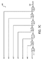
図6には、組合わせ論理414のための真理値表600が示されている。
In FIG. 6, a truth table 600 for
H−SCC206が5:1分圧器として動作するために、H−SCC段206が動作し得る複数の動作領域を定める7つの変換比閾値限界(mth1〜mth7で示される)のうちの1つによって構成される7つの比較器412が使用される。
In order for H-
7つの比較器412は、それぞれ、組合わせ論理614への入力として受信される出力信号(m1〜m7)を供給する。論理段416、418、及び420は、それぞれ、上記信号(m1〜m7)を入力として受信する。 Each of the seven comparators 412 provides an output signal (m1-m7) that is received as an input to the combinational logic 614. Each of the logic stages 416, 418, and 420 receives the signals (m1 to m7) as inputs.
組合わせ論理614の真理値表600の第1の行は、計算された要求される変換比mが変換比閾値限界mth1よりも小さい場合、比較器412aの出力がハイ(m1=1)であることを示し、よって、H−SCC段206は第1の動作領域で動作し、組合わせ論理414は、フェーズφ1において奇数スイッチに
![]()
![]()
組合わせ論理614の真理値表600の第2の行は、計算された要求される変換比mが変換比閾値限界mth1と変換比閾値限界mth2との間の場合、比較器412bの出力がハイ(m2=1)であることを示し、よって、H−SCC段206は第2の動作領域で動作し、組合わせ論理414は、フェーズφ1において奇数スイッチに
![]()
![]()
上記の説明から、真理値表600から、H−SCC段206が第3〜第7の動作領域で動作しているときに、組み合わせ論理614が動作のためにどのように構成されるかは明らかであろう。
From the above description, it is clear from truth table 600 how combinational logic 614 is configured for operation when H-
論理段418の出力ch2、ch1、及びch0 224に応じて、複数のマルチプレクサチャネルのうちの1つが選択される。具体的には、ch2=0、ch1=0、ch0=0の場合にマルチプレクサ210の第1のチャネル(CH1)が選択され、ch2=0、ch1=0、ch0=1の場合にマルチプレクサ210の第2のチャネル(CH2)が選択され、ch2=0、ch1=1、ch0=0の場合にマルチプレクサ210の第3のチャネル(CH3)が選択され、ch2=0、ch1=1、ch0=1の場合にマルチプレクサ210の第4のチャネル(CH4)が選択され、ch2=1、ch1=0、ch0=0の場合にマルチプレクサ210の第5のチャネル(CH5)が選択される。
Depending on the outputs ch2, ch1, and ch0 224 of
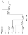
論理段416の例が図7aに示されている。論理段416は、7つの比較器412から出力される信号m1〜m7を入力として受け取る。真理値表600に従うために、複数の論理ゲートの配列が論理段416内に設けられている。例示的な論理段416が図7aに示されているが、実施形態は、真理値表600に従う論理ゲートの他の構成に及ぶ。
An example of
論理段418の例が図7bに示されている。論理段418は、7つの比較器412から出力される信号m1〜m7を入力として受け取る。真理値表600に従うために、複数の論理ゲートの配列が論理段418内に設けられている。例示的な論理段418が図7bに示されているが、実施形態は、真理値表600に従う論理ゲートの他の構成に及ぶ。
An example of
論理段420の例が図7cに示されている。論理段420は、7つの比較器412から出力される信号m1〜m7を入力として受け取る。真理値表600に従うために、複数の論理ゲートの配列が論理段420内に設けられている。例示的な論理段420が図7bに示されているが、実施形態は、真理値表600に従う論理ゲートの他の構成に及ぶ。
An example of
H−SCC段206が動作領域OZ0、OZ2、OZ4、及びOZ6で動作しているとき、コントローラ216はH−SCC段206を5:1分圧器(第1の変換比M1)として動作するように制御する。H−SCC段206が動作領域OZ1、OZ3、OZ5、及びOZ7で動作しているとき、コントローラ216はH−SCC段206を4.5:1分圧器(第2の変換比M2)として動作するように制御する。
When the H-
図8は、上記実施形態に従って動作する電力変換装置200の効率対変換比曲線を示す。
FIG. 8 shows an efficiency versus conversion ratio curve of the
図8に示されるように、複数の特定の変換比閾値限界によって規定される図8の複数の動作領域のうちの1つ(HP=オフとして記される)においてH−SCC206が動作している場合、コントローラ216は、電力変換装置200を5:1分圧器(変換比M1)として動作するよう制御するためにハーフポイント段204を第1の動作モードで動作するよう制御する。さらに、複数の特定の変換比閾値限界によって規定される図8の複数の動作領域のうちの1つ(HP=オンとして記される)においてH−SCC206が動作している場合、コントローラ216は、電力変換装置200を4.5:1分圧器(変換比M2)として動作するよう制御するためにハーフポイント段204を第2の動作モードで動作するよう制御する。
As shown in FIG. 8, the H-
図8に示すように、第1の変換比M1及び第2の変換比M2を供給するように動作するH−SCC206のこの切り替えは、要求される変換比mが増加するにつれて継続する。
As shown in FIG. 8, this switching of the H-
図8の曲線から理解されるように、上記実施形態に従って動作する電力変換装置200は、効率性能を一層改善することを可能にし、変換範囲全体から効率低下がほぼ除去される。
As can be understood from the curve of FIG. 8, the
図8は、要求される変換比mが各変換比閾値範囲の間にある場合の組合わせ論理614の出力を示す。例えば、要求される変換比mが変換比閾値mth1とmth2との間にある場合、H−SCC206は動作領域OZ1で動作し、したがって、マルチプレクサ409は、フェーズφ1において奇数スイッチに
![]()
![]()
異なる出力電流Ioを表す各曲線について、効率ノッチは常に同じ変換比に位置することが分かる。 It can be seen that for each curve representing a different output current Io , the efficiency notch is always located at the same conversion ratio.
図9は、変化される目標基準電圧Vsetに依存する、5:1分圧器及び4.5:1分圧器として動作するよう構成されたH−SCC段206のシミュレーション結果を示す。
FIG. 9 shows the simulation results of the H-
図9に示すように、目標基準電圧Vsetが第1の電圧レベルに設定される場合、H−SCC段206は動作領域OZ2で動作し、ある時間の経過後、出力電圧は目標基準電圧Vsetに落ち着く。目標基準電圧Vsetが第2の電圧レベルに変更される場合、H−SCC段206は動作領域OZ7で動作し、ある時間の経過後、出力電圧は目標基準電圧Vsetに落ち着く。目標基準電圧Vsetが第3の電圧レベルに変更される場合、H−SCC段206は動作領域OZ5で動作し、ある時間の経過後、出力電圧は目標基準電圧Vsetに落ち着く。
As shown in FIG. 9, when the target reference voltage V set is set to the first voltage level, the H-
上記では、H−SCC段206の変換比を0.5だけシフトするためにハーフポイントSCC204を使用して実装される変換比制御段204に関して実施形態を説明した。本発明の実施形態は、このような変換比制御段に限定されない。H−SCC段206の変換比の交換は、デューティサイクルに対する効率曲線の変化を達成するという利点を有する。変換比制御段204の他の実装形態でも同様の効果を達成することができる。
Above, embodiments have been described with respect to a conversion
図10は、第1のスイッチSx1及び第2のスイッチSx2を含むフルポイントSCC204を示す。スイッチSx1の入力端子は電圧源202に接続され、スイッチSx1の出力端子は中央ノードN1に接続される。スイッチSx2の入力端子は電圧源202に接続され、スイッチSx2の出力端子は中央ノードN2に接続される。
FIG. 10 shows a
フルポイントSCC204は、2つのスイッチ構成のうちの1つに従って制御することができる。
The
第1のスイッチ構成では、第1の時間フェーズΦ1の間はスイッチSx1及びSx2がオフにされ、第2の時間フェーズΦ2の間はスイッチSx1がオンにされ、スイッチSx2がオフにされ、スイッチSx2及びSx4はオフにされる。すなわち、第2の時間フェーズΦ2の間、電圧VinがH−SCC206の第1の中央ノードN1に供給される。
In the first switch configuration, the switches Sx1 and Sx2 are turned off during the first time phase Φ1, the switch Sx1 is turned on, the switch Sx2 is turned off, and the switch Sx2 during the second time phase Φ2. And Sx4 are turned off. That is, during the second
第2のスイッチ構成では、第1の時間フェーズΦ1の間はスイッチSx1がオフにされ、スイッチSx2がオンにされる一方、第2の時間フェーズΦ2の間はスイッチSx1及びSx2がオフにされる。すなわち、第1の時間フェーズΦ1の間、電圧VinがH−SCC206の第2の中央ノードN2に供給される。
In the second switch configuration, switch Sx1 is turned off and switch Sx2 is turned on during the first time phase Φ1, while switches Sx1 and Sx2 are turned off during the second time phase Φ2. . That is, during the first time phase Φ1, the voltage Vin is supplied to the second central node N2 of the H-
すなわち、電力変換装置200の変換比は、以下の表2に示すように、フルポイントSCC204のスイッチ構成を制御することによって構成することができる。
表2に示されるように、フルポイントSCC204が第1の動作モードで動作する場合(上述の第1のスイッチ構成に従って)、電力変換装置200は、5:1分圧器、すなわち、5分割分圧器(第1の変換比M1(1/5)を有する)として動作する。フルポイントSCC204が第2の動作モードで動作する場合(上述の第2のスイッチ構成に従って)、電力変換装置200の変換比は1だけ低減され、この場合、電力変換装置200は4:1分圧器、すなわち、4。5分割分圧器(第2の変換比M2(1/4)を有する)として動作する。
As shown in Table 2, when full-
4:1分圧器として動作する場合、SCC段208の出力電圧は以下の通りである。
図11は、5:1分圧器として動作する場合の電力変換装置200の効率対変換比曲線1102を示し、4:1分圧器として動作する場合の電力変換装置200の効率対変換比曲線1104を示す。
FIG. 11 shows the efficiency versus
H−SCC段206がM1として記される動作領域のうちの1つで動作しているとき、コントローラ216はH−SCC段206を5:1分圧器(第1の変換比M1)として動作するように制御する。H−SCC段206がM2として記される動作領域のうちの1つで動作しているとき、コントローラ216はH−SCC段206を4.5:1分圧器(第2の変換比M2)として動作するように制御する。これにより、効率ノッチを克服することが可能となり、効率性能が改善される。
When the H-
H−SCC段206の前の電力線入力に変換比制御段204を配置する上述の実施形態では、変換比制御段204の動作モードは切り替えられ、H−SCC段の変換比はシフトされる一方、SCC段208のスイッチング構成は一定のままである。
In the above embodiment where the conversion
上述したように、H−SCC段206の前の電力線入力に配置する代わりに、変換比制御段204を(図2bに示すように)H−SCC206段内に組み込むこともできる。
As mentioned above, instead of being placed at the power line input in front of the H-
これらの代替的実施形態では、変換比制御段204の動作モード及びSCC段208のスイッチング構成の両方を切り替えて、H−SCC段206の変換比がシフトされる。
In these alternative embodiments, the conversion ratio of the H-
図12は、変換比制御段204がH−SCC段206内に統合された構成例を示す。特に、図12は、変換比制御段204とH−SCC段206のSCC段208との結合を示す。
FIG. 12 shows a configuration example in which the conversion
図12において、SCC段208は、スイッチM1、M2、M3、M5、M6、M8、及びM9を含む3:2分圧器である。
In FIG. 12,
SCC段208の第1のスイッチ構成では、第1の時間フェーズΦ1の間、スイッチM1、M3、M6、及びM8はオンにされる一方、スイッチM2、M5、及びM9はオフにされ、後続する第2の時間フェーズΦ2の間、全てのスイッチM1〜M3、M5、M6、M8、及びM9の状態が反転される。コントローラ216は、上述のように、第1の時間フェーズΦ1及び第2の時間フェーズΦ2においてスイッチ(M1、M2、M3、M5、M6、M8、及びM9)を制御するPWM信号を生成するように構成される。
In the first switch configuration of
図12に示す例では、変換比制御段204は、スイッチM4及びM7を備える。第1の動作モードで動作するとき、変換比制御段204のスイッチM4及びM7は、第1の時間フェーズΦ1及び第2の時間フェーズΦ2の両方においてオフにされる。変換比制御段204が第1の動作モードで動作するように制御され、SCC段208が上記第1のスイッチ構成に従って制御される場合、SCC段208は3:2分圧器として動作する。
In the example shown in FIG. 12, the conversion
3:2分圧器として動作する場合、SCC段208の出力電圧は以下の通りである。
3:2分圧器の出力変換比範囲を拡張するために、コントローラ216は、変換比制御段204の動作モードを第2の動作モードに切り替え、SCC段208のスイッチ構成を変更するように動作可能である。
To extend the output conversion ratio range of the 3: 2 voltage divider, the
SCC段208の第2のスイッチ構成では、第1の時間フェーズΦ1の間、(3:2分圧器動作と同様に)スイッチM1、M3、M6、及びM8はオンにされる一方、スイッチM2、M4、M7、及びM9はオフにされ、後続する第2の時間フェーズΦ2の間、全てのスイッチの状態が反転される。スイッチM5は、第1の時間フェーズΦ1及び第2の時間フェーズΦ2の両方の間オフにされる。コントローラ216は、上述のように、第1の時間フェーズΦ1及び第2の時間フェーズΦ2においてスイッチ(M1〜M4及びM6〜M9)を制御するPWM信号を生成するように構成される。
In the second switch configuration of
第2の動作モードで動作するとき、変換比制御段204のスイッチM4及びM7は、第1の時間フェーズΦ1の間はオフにされ、第2の時間フェーズΦ2の間はオンにされる。変換比制御段204が第2の動作モードで動作するように制御され、SCC段208が上記第2のスイッチ構成に従って制御される場合、SCC段208は2:1分圧器として動作する。
When operating in the second mode of operation, the switches M4 and M7 of the conversion
2:1分圧器として動作する場合、SCC段208の出力電圧は以下の通りである。
図13には、SCC段208が3:2分圧器及び2:1分圧器の両方として動作するよう制御される場合のスイッチM1〜M9の状態が示されている。
FIG. 13 shows the state of switches M1-M9 when
図12に示す構成例では、H−SCC段206の出力フィルタ212がノードVx4に接続される場合、このノードは2つの変換比を提供する出力電圧を供給する。SCC段208が2:1分圧器として構成される場合、ノードVx4は、変換比Vo/Vin=(2−D)/2を提供する(ここで、DはSCC段208のスイッチに供給されるPWM信号のデューティサイクル)。SCC段208が3:2分圧器として構成される場合、ノードVx4は、変換比Vo/Vin=(3−D)/3を提供する。
In the example configuration shown in FIG. 12, when the
本発明の実施形態は、H−SCC段206の変換比を、本明細書が与える実施例に記載される量とは異なる量シフトさせる変換比制御段204の実装形態に及ぶ。
Embodiments of the present invention extend to implementations of conversion
実施形態では、H−SCC段206の変換比の変化は、効率ノッチを克服することを可能にする効率曲線のシフトをもたらす。変換比のシフト量とインダクタに加えられるリップルとの間にはトレードオフが存在する。変換比が減少(シフト)されると、インダクタにおける電圧リップルが増加し、より大きいインダクタが要求されるため、システム全体のボリュームが損なわれる。したがって、変換比シフトが大きければ大きいほど、インダクタにおける電圧リップルの増加が大きくなり、より大きいインダクタが要求される。
In an embodiment, the change in the conversion ratio of the H-
図示の実施形態のように、スイッチS1〜S8及びM1〜M9の全ては双方向であり、回路のスイッチング周波数に適合する適切な技術で実装され得る。例えば、スイッチは、シリコン基板上のMOSFET(Metal Oxide Semiconductor Field Effect Transistors)、又は窒化ガリウム基板上のHEMT(High Electron Mobility Transistors)によって形成され得る。 As in the illustrated embodiment, all of the switches S1-S8 and M1-M9 are bi-directional and can be implemented with a suitable technique that matches the switching frequency of the circuit. For example, the switch can be formed by a MOSFET (Metal Oxide Field Effect Transistors) on a silicon substrate, or a HEMT (High Electron Mobility Transistors) on a gallium nitride substrate.
上述の実施形態に含まれる全ての要素は、例えばPSoC(Power System on a Chip)又はPSiP(Power System in a Package)としての集積を可能にするのに十分に小さいサイズに設計され得る。図示の例示的な実施形態では、全てのキャパシタについて、キャパシタンスは100nFに設定することができる。また、より良い性能を達成するためにキャパシタンス値をさらに最適化することができる。フィルタインダクタLoのインダクタンス値は200nHに設定することができ、これは、5x5mmの表面を有するLEDサブマウントに印刷することを可能にする。例えば、LEDパッケージは、少なくとも1つのLEDと、各実施形態で説明したような電力変換装置を含むドライバとを含むように設計することができる。 All elements included in the above-described embodiments can be designed to be small enough to allow integration, for example as PSOC (Power System on a Chip) or PSiP (Power System in a Package). In the illustrated exemplary embodiment, the capacitance can be set to 100 nF for all capacitors. Also, the capacitance value can be further optimized to achieve better performance. The inductance value of the filter inductor Lo can be set to 200 nH, which makes it possible to print on an LED submount with a 5 × 5 mm surface. For example, the LED package can be designed to include at least one LED and a driver that includes a power converter as described in each embodiment.
キャパシタは、FRAM(登録商標)(Ferroelectric Random Access Memory)又はeDRAM(embedded Dynamic Random Access Memory)に適用される技術と同様の技術を用いて実装されてもよい。このような技術によって達成されるより高い誘電率は、集積SCCをより小さくかつ安価にすることを可能にする。 The capacitor may be mounted using a technique similar to that applied to FRAM (registered trademark) (Ferroelectric Random Access Memory) or eDRAM (Embedded Dynamic Random Access Memory). The higher dielectric constant achieved by such techniques allows the integrated SCC to be smaller and cheaper.
本発明は、図面及び上記において詳細に図示及び記載されているが、かかる図示及び記載は説明的又は例示的であり、非限定的であると考えられるべきであることは当業者には明らかであろう。本発明は開示の実施形態に限定されず、むしろ、添付の特許請求の範囲に規定される本発明の保護範囲内で複数の変形及び変更が可能である。 While the invention has been illustrated and described in detail in the drawings and foregoing, it will be clear to those skilled in the art that such illustration and description are to be considered illustrative or exemplary and not restrictive. I will. The invention is not limited to the disclosed embodiments, but rather may be varied and modified within the protection scope of the invention as defined in the appended claims.
例えば、上記実施形態は、特定のトポロジーのSCCによって形成される電力変換モジュールに関するものであるが、他のタイプの電力変換器が使用されてもよい。 For example, although the above embodiment relates to a power conversion module formed by SCC of a specific topology, other types of power converters may be used.
本明細書では、負荷が光源である用途が主に説明されているが、本発明は、例えば物理的又は生理的パラメータを検出するためのインプラント可能又は装着可能なセンサ等の集積デバイス、又は集積エネルギー・ハーベスト・ユニット等、集積電力管理ユニットを必要とする多数のシステムにも適用され得る。 Although the present application primarily describes applications where the load is a light source, the present invention is not limited to an integrated device, such as an implantable or wearable sensor for detecting physical or physiological parameters, or integration. It can also be applied to many systems that require an integrated power management unit, such as an energy harvesting unit.
コントローラ216は、アナログ回路を使用して実装されるように図示されているが、他の実施形態では、コントローラ216の機能は、1つ又は複数の記憶媒体を含むメモリに格納され、1つ又は複数の処理装置を含むプロセッサ上で実行されるよう構成されたコード(ソフトウェア)に実装され得る。コードは、メモリから取り出されてプロセッサ上で実行されると、上述の実施形態に則する動作を実行するように構成されている。
Although the
開示の実施形態の他の変形例が、図面、開示、及び添付の特許請求の範囲から、クレームされる発明に係る当業者によって理解及び実施され得る。特許請求の範囲において、「含む(comprising)」という用語は他の要素又はステップを排除するものではなく、不定冠詞「a」又は「an」は複数を除外しない。複数の手段が互いに異なる従属請求項に記載されているからといって、これらの手段の組み合わせが好適に使用することができないとは限らない。特許請求の範囲内のいかなる参照符号も、その範囲を限定するものと解釈されるべきではない。 Other variations of the disclosed embodiments can be understood and implemented by those skilled in the art of the claimed invention from the drawings, disclosure, and appended claims. In the claims, the term “comprising” does not exclude other elements or steps, and the indefinite article “a” or “an” does not exclude a plurality. Just because a plurality of means are recited in different dependent claims does not necessarily mean that a combination of these means cannot be suitably used. Any reference signs in the claims should not be construed as limiting the scope.
Claims (15)
DC入力電圧によって供給され、複数の出力信号を供給する電力変換モジュールであって、前記誘導出力フィルタは前記複数の出力信号のうちの1つを受信する、電力変換モジュールと、
前記電力変換モジュールに結合された変換比制御段と、
前記DC入力電圧及び目標基準電圧に基づき、要求される変換比を決定し、決定された前記要求される変換比に基づき、前記変換比制御段を第1の動作モード及び第2の動作モードのうちの1つで動作するよう制御するコントローラと
を含み、
前記変換比制御段が前記第1の動作モードで動作する場合、前記電力変換モジュールは第1の変換比に従って前記複数の出力信号を供給し、前記変換比制御段が前記第2の動作モードで動作する場合、前記電力変換モジュールは第2の変換比に従って前記複数の出力信号を供給する、
電力変換装置。 A power conversion device comprising an inductive output filter having at least an output connected to a load, for supplying a pulse width modulation (PWM) signal to the load, the power conversion device comprising:
A power conversion module that is supplied with a DC input voltage and provides a plurality of output signals, wherein the inductive output filter receives one of the plurality of output signals;
A conversion ratio control stage coupled to the power conversion module;
A required conversion ratio is determined based on the DC input voltage and the target reference voltage, and the conversion ratio control stage is set to the first operation mode and the second operation mode based on the determined conversion ratio. A controller that controls to operate with one of them,
When the conversion ratio control stage operates in the first operation mode, the power conversion module supplies the plurality of output signals according to a first conversion ratio, and the conversion ratio control stage operates in the second operation mode. When operating, the power conversion module provides the plurality of output signals according to a second conversion ratio.
Power conversion device.
Applications Claiming Priority (3)
| Application Number | Priority Date | Filing Date | Title |
|---|---|---|---|
| EP15150332.3 | 2015-01-07 | ||
| EP15150332 | 2015-01-07 | ||
| PCT/EP2015/081107 WO2016110413A1 (en) | 2015-01-07 | 2015-12-23 | Power conversion device. |
Publications (2)
| Publication Number | Publication Date |
|---|---|
| JP2018501767A true JP2018501767A (en) | 2018-01-18 |
| JP2018501767A5 JP2018501767A5 (en) | 2019-01-10 |
Family
ID=52232103
Family Applications (1)
| Application Number | Title | Priority Date | Filing Date |
|---|---|---|---|
| JP2017535898A Pending JP2018501767A (en) | 2015-01-07 | 2015-12-23 | Power converter |
Country Status (6)
| Country | Link |
|---|---|
| US (1) | US10218267B2 (en) |
| EP (1) | EP3243265A1 (en) |
| JP (1) | JP2018501767A (en) |
| CN (1) | CN107112893A (en) |
| RU (1) | RU2017127532A (en) |
| WO (1) | WO2016110413A1 (en) |
Families Citing this family (6)
| Publication number | Priority date | Publication date | Assignee | Title |
|---|---|---|---|---|
| DE102015224476A1 (en) * | 2015-12-07 | 2017-06-08 | Dialog Semiconductor (Uk) Limited | Multi-level down-to-up converter with high efficiency |
| US11362587B2 (en) * | 2017-08-15 | 2022-06-14 | Texas Instruments Incorporated | Hysteretic pulse modulation for charge balance of multi-level power converters |
| EP3484034A1 (en) | 2017-11-14 | 2019-05-15 | GN Hearing A/S | A switched capacitor dc-dc converter comprising external and internal flying capacitors |
| CN109688659A (en) * | 2018-12-21 | 2019-04-26 | 太仓电威光电有限公司 | LED drive power mould group and the integral LED car light for applying it |
| US11502599B2 (en) * | 2019-09-18 | 2022-11-15 | Qualcomm Incorporated | Constant gate-to-source-volt age-driving driver architecture for switched-mode power supplies |
| CN115191152A (en) * | 2020-02-27 | 2022-10-14 | 昕诺飞控股有限公司 | Hybrid switched capacitor circuit with automatic charge balancing |
Citations (3)
| Publication number | Priority date | Publication date | Assignee | Title |
|---|---|---|---|---|
| JP2009247093A (en) * | 2008-03-31 | 2009-10-22 | Kaga Electronics Co Ltd | Multiple-output dc-dc converter |
| US20120169405A1 (en) * | 2011-01-03 | 2012-07-05 | Choi Won-Beom | Method and apparatus for generating voltage |
| WO2014077355A1 (en) * | 2012-11-15 | 2014-05-22 | 太陽誘電株式会社 | Power conversion device |
Family Cites Families (6)
| Publication number | Priority date | Publication date | Assignee | Title |
|---|---|---|---|---|
| US7417488B2 (en) * | 2005-11-04 | 2008-08-26 | Intel Corporation | Regulation circuit for inductive charge pump |
| US7696735B2 (en) * | 2007-03-30 | 2010-04-13 | Intel Corporation | Switched capacitor converters |
| US8710903B2 (en) | 2008-06-30 | 2014-04-29 | Intel Corporation | Drive and startup for a switched capacitor divider |
| US8259476B2 (en) | 2008-07-29 | 2012-09-04 | Shmuel Ben-Yaakov | Self-adjusting switched-capacitor converter with multiple target voltages and target voltage ratios |
| JP2011050209A (en) * | 2009-08-28 | 2011-03-10 | Japan Aerospace Exploration Agency | Electric double-layer capacitor power supply using intermediate tap in switched capacitor system |
| WO2013086445A1 (en) | 2011-12-09 | 2013-06-13 | The Regents Of The University Of California | Switched-capacitor isolated led driver |
-
2015
- 2015-12-23 US US15/541,657 patent/US10218267B2/en not_active Expired - Fee Related
- 2015-12-23 WO PCT/EP2015/081107 patent/WO2016110413A1/en active Application Filing
- 2015-12-23 EP EP15823603.4A patent/EP3243265A1/en not_active Withdrawn
- 2015-12-23 CN CN201580072673.0A patent/CN107112893A/en active Pending
- 2015-12-23 RU RU2017127532A patent/RU2017127532A/en not_active Application Discontinuation
- 2015-12-23 JP JP2017535898A patent/JP2018501767A/en active Pending
Patent Citations (3)
| Publication number | Priority date | Publication date | Assignee | Title |
|---|---|---|---|---|
| JP2009247093A (en) * | 2008-03-31 | 2009-10-22 | Kaga Electronics Co Ltd | Multiple-output dc-dc converter |
| US20120169405A1 (en) * | 2011-01-03 | 2012-07-05 | Choi Won-Beom | Method and apparatus for generating voltage |
| WO2014077355A1 (en) * | 2012-11-15 | 2014-05-22 | 太陽誘電株式会社 | Power conversion device |
Also Published As
| Publication number | Publication date |
|---|---|
| CN107112893A (en) | 2017-08-29 |
| US20180006552A1 (en) | 2018-01-04 |
| EP3243265A1 (en) | 2017-11-15 |
| RU2017127532A3 (en) | 2019-05-21 |
| US10218267B2 (en) | 2019-02-26 |
| RU2017127532A (en) | 2019-02-07 |
| WO2016110413A1 (en) | 2016-07-14 |
Similar Documents
| Publication | Publication Date | Title |
|---|---|---|
| JP6138973B2 (en) | Compact power converter with continuous output adjustment range | |
| US10498236B2 (en) | Two-phase three-level converter and controller therefor | |
| JP2018501767A (en) | Power converter | |
| US9653986B2 (en) | Multi-level step-up converter topologies, control and soft start systems and methods | |
| US10034334B2 (en) | Driver circuit with extended operation range | |
| US9093901B2 (en) | Switching converter and method for controlling a switching converter | |
| JP6430519B2 (en) | Compact driver especially for light-emitting diodes with auxiliary output | |
| USRE46256E1 (en) | Asymmetric topology to boost low load efficiency in multi-phase switch-mode power conversion | |
| JP6143951B2 (en) | Compact driver with integrated dual output, especially for light emitting diodes | |
| KR101935452B1 (en) | The dc-dc converter and the two-stage power converter including dc-dc converter | |
| CN111277139A (en) | Stacked buck converter | |
| CN104852568B (en) | Current source based on Cuk | |
| US20110249474A1 (en) | Method and apparatus for power conversion using an interleaved flyback converter with alternating master and slave branches | |
| KR101677705B1 (en) | Multiple output switched capacitor dc-dc converter | |
| JP2016509371A (en) | Light emitting diode driver with differential voltage supply | |
| WO2018116349A1 (en) | Power conversion device and electric propulsion system | |
| JP2010200519A (en) | Boosting chopper circuit | |
| KR101549436B1 (en) | Driving circuit for lighting emitting diode using delay routine and driving method thereof | |
| JP6760102B2 (en) | Lighting device and lighting equipment | |
| Kopylov et al. | The pump current pulse generator for laser diodes | |
| US20120112659A1 (en) | LED Circuit Having LED Driving Circuit and Operation Method of the Same |
Legal Events
| Date | Code | Title | Description |
|---|---|---|---|
| RD02 | Notification of acceptance of power of attorney |
Free format text: JAPANESE INTERMEDIATE CODE: A7422 Effective date: 20180524 |
|
| RD04 | Notification of resignation of power of attorney |
Free format text: JAPANESE INTERMEDIATE CODE: A7424 Effective date: 20180619 |
|
| A521 | Request for written amendment filed |
Free format text: JAPANESE INTERMEDIATE CODE: A523 Effective date: 20181120 |
|
| A621 | Written request for application examination |
Free format text: JAPANESE INTERMEDIATE CODE: A621 Effective date: 20181120 |
|
| A131 | Notification of reasons for refusal |
Free format text: JAPANESE INTERMEDIATE CODE: A131 Effective date: 20191001 |
|
| A977 | Report on retrieval |
Free format text: JAPANESE INTERMEDIATE CODE: A971007 Effective date: 20190927 |
|
| A02 | Decision of refusal |
Free format text: JAPANESE INTERMEDIATE CODE: A02 Effective date: 20200702 |