JP2018200823A - Connector device - Google Patents
Connector device Download PDFInfo
- Publication number
- JP2018200823A JP2018200823A JP2017105281A JP2017105281A JP2018200823A JP 2018200823 A JP2018200823 A JP 2018200823A JP 2017105281 A JP2017105281 A JP 2017105281A JP 2017105281 A JP2017105281 A JP 2017105281A JP 2018200823 A JP2018200823 A JP 2018200823A
- Authority
- JP
- Japan
- Prior art keywords
- terminal
- housing
- connection
- current sensor
- current
- Prior art date
- Legal status (The legal status is an assumption and is not a legal conclusion. Google has not performed a legal analysis and makes no representation as to the accuracy of the status listed.)
- Abandoned
Links
- 230000004907 flux Effects 0.000 claims abstract description 11
- 230000008878 coupling Effects 0.000 claims abstract description 5
- 238000010168 coupling process Methods 0.000 claims abstract description 5
- 238000005859 coupling reaction Methods 0.000 claims abstract description 5
- 238000005259 measurement Methods 0.000 claims description 16
- 230000005389 magnetism Effects 0.000 claims description 3
- 230000008054 signal transmission Effects 0.000 description 6
- 238000003780 insertion Methods 0.000 description 5
- 230000037431 insertion Effects 0.000 description 5
- WABPQHHGFIMREM-UHFFFAOYSA-N lead(0) Chemical compound [Pb] WABPQHHGFIMREM-UHFFFAOYSA-N 0.000 description 4
- 239000002184 metal Substances 0.000 description 3
- 238000001514 detection method Methods 0.000 description 2
- 239000000696 magnetic material Substances 0.000 description 2
- 229910000859 α-Fe Inorganic materials 0.000 description 2
- 239000004020 conductor Substances 0.000 description 1
- 238000002788 crimping Methods 0.000 description 1
- 238000000605 extraction Methods 0.000 description 1
- 239000011810 insulating material Substances 0.000 description 1
- 239000007788 liquid Substances 0.000 description 1
- 230000013011 mating Effects 0.000 description 1
- 238000000034 method Methods 0.000 description 1
- 238000004382 potting Methods 0.000 description 1
- 229920003002 synthetic resin Polymers 0.000 description 1
- 239000000057 synthetic resin Substances 0.000 description 1
Images


Classifications
-
- H—ELECTRICITY
- H01—ELECTRIC ELEMENTS
- H01R—ELECTRICALLY-CONDUCTIVE CONNECTIONS; STRUCTURAL ASSOCIATIONS OF A PLURALITY OF MUTUALLY-INSULATED ELECTRICAL CONNECTING ELEMENTS; COUPLING DEVICES; CURRENT COLLECTORS
- H01R13/00—Details of coupling devices of the kinds covered by groups H01R12/70 or H01R24/00 - H01R33/00
- H01R13/66—Structural association with built-in electrical component
- H01R13/665—Structural association with built-in electrical component with built-in electronic circuit
- H01R13/6683—Structural association with built-in electrical component with built-in electronic circuit with built-in sensor
-
- H—ELECTRICITY
- H01—ELECTRIC ELEMENTS
- H01R—ELECTRICALLY-CONDUCTIVE CONNECTIONS; STRUCTURAL ASSOCIATIONS OF A PLURALITY OF MUTUALLY-INSULATED ELECTRICAL CONNECTING ELEMENTS; COUPLING DEVICES; CURRENT COLLECTORS
- H01R31/00—Coupling parts supported only by co-operation with counterpart
- H01R31/06—Intermediate parts for linking two coupling parts, e.g. adapter
- H01R31/065—Intermediate parts for linking two coupling parts, e.g. adapter with built-in electric apparatus
-
- G—PHYSICS
- G01—MEASURING; TESTING
- G01R—MEASURING ELECTRIC VARIABLES; MEASURING MAGNETIC VARIABLES
- G01R1/00—Details of instruments or arrangements of the types included in groups G01R5/00 - G01R13/00 and G01R31/00
- G01R1/02—General constructional details
- G01R1/04—Housings; Supporting members; Arrangements of terminals
- G01R1/0408—Test fixtures or contact fields; Connectors or connecting adaptors; Test clips; Test sockets
- G01R1/0416—Connectors, terminals
-
- G—PHYSICS
- G01—MEASURING; TESTING
- G01R—MEASURING ELECTRIC VARIABLES; MEASURING MAGNETIC VARIABLES
- G01R15/00—Details of measuring arrangements of the types provided for in groups G01R17/00 - G01R29/00, G01R33/00 - G01R33/26 or G01R35/00
- G01R15/14—Adaptations providing voltage or current isolation, e.g. for high-voltage or high-current networks
- G01R15/20—Adaptations providing voltage or current isolation, e.g. for high-voltage or high-current networks using galvano-magnetic devices, e.g. Hall-effect devices, i.e. measuring a magnetic field via the interaction between a current and a magnetic field, e.g. magneto resistive or Hall effect devices
- G01R15/207—Constructional details independent of the type of device used
-
- G—PHYSICS
- G01—MEASURING; TESTING
- G01R—MEASURING ELECTRIC VARIABLES; MEASURING MAGNETIC VARIABLES
- G01R33/00—Arrangements or instruments for measuring magnetic variables
- G01R33/02—Measuring direction or magnitude of magnetic fields or magnetic flux
-
- H—ELECTRICITY
- H01—ELECTRIC ELEMENTS
- H01R—ELECTRICALLY-CONDUCTIVE CONNECTIONS; STRUCTURAL ASSOCIATIONS OF A PLURALITY OF MUTUALLY-INSULATED ELECTRICAL CONNECTING ELEMENTS; COUPLING DEVICES; CURRENT COLLECTORS
- H01R13/00—Details of coupling devices of the kinds covered by groups H01R12/70 or H01R24/00 - H01R33/00
- H01R13/02—Contact members
-
- H—ELECTRICITY
- H01—ELECTRIC ELEMENTS
- H01R—ELECTRICALLY-CONDUCTIVE CONNECTIONS; STRUCTURAL ASSOCIATIONS OF A PLURALITY OF MUTUALLY-INSULATED ELECTRICAL CONNECTING ELEMENTS; COUPLING DEVICES; CURRENT COLLECTORS
- H01R13/00—Details of coupling devices of the kinds covered by groups H01R12/70 or H01R24/00 - H01R33/00
- H01R13/46—Bases; Cases
- H01R13/502—Bases; Cases composed of different pieces
-
- H—ELECTRICITY
- H01—ELECTRIC ELEMENTS
- H01R—ELECTRICALLY-CONDUCTIVE CONNECTIONS; STRUCTURAL ASSOCIATIONS OF A PLURALITY OF MUTUALLY-INSULATED ELECTRICAL CONNECTING ELEMENTS; COUPLING DEVICES; CURRENT COLLECTORS
- H01R13/00—Details of coupling devices of the kinds covered by groups H01R12/70 or H01R24/00 - H01R33/00
- H01R13/66—Structural association with built-in electrical component
- H01R13/665—Structural association with built-in electrical component with built-in electronic circuit
- H01R13/6691—Structural association with built-in electrical component with built-in electronic circuit with built-in signalling means
-
- H—ELECTRICITY
- H01—ELECTRIC ELEMENTS
- H01R—ELECTRICALLY-CONDUCTIVE CONNECTIONS; STRUCTURAL ASSOCIATIONS OF A PLURALITY OF MUTUALLY-INSULATED ELECTRICAL CONNECTING ELEMENTS; COUPLING DEVICES; CURRENT COLLECTORS
- H01R24/00—Two-part coupling devices, or either of their cooperating parts, characterised by their overall structure
- H01R24/28—Coupling parts carrying pins, blades or analogous contacts and secured only to wire or cable
-
- G—PHYSICS
- G01—MEASURING; TESTING
- G01R—MEASURING ELECTRIC VARIABLES; MEASURING MAGNETIC VARIABLES
- G01R15/00—Details of measuring arrangements of the types provided for in groups G01R17/00 - G01R29/00, G01R33/00 - G01R33/26 or G01R35/00
- G01R15/14—Adaptations providing voltage or current isolation, e.g. for high-voltage or high-current networks
- G01R15/20—Adaptations providing voltage or current isolation, e.g. for high-voltage or high-current networks using galvano-magnetic devices, e.g. Hall-effect devices, i.e. measuring a magnetic field via the interaction between a current and a magnetic field, e.g. magneto resistive or Hall effect devices
- G01R15/202—Adaptations providing voltage or current isolation, e.g. for high-voltage or high-current networks using galvano-magnetic devices, e.g. Hall-effect devices, i.e. measuring a magnetic field via the interaction between a current and a magnetic field, e.g. magneto resistive or Hall effect devices using Hall-effect devices
-
- G—PHYSICS
- G01—MEASURING; TESTING
- G01R—MEASURING ELECTRIC VARIABLES; MEASURING MAGNETIC VARIABLES
- G01R19/00—Arrangements for measuring currents or voltages or for indicating presence or sign thereof
- G01R19/0092—Arrangements for measuring currents or voltages or for indicating presence or sign thereof measuring current only
-
- H—ELECTRICITY
- H01—ELECTRIC ELEMENTS
- H01R—ELECTRICALLY-CONDUCTIVE CONNECTIONS; STRUCTURAL ASSOCIATIONS OF A PLURALITY OF MUTUALLY-INSULATED ELECTRICAL CONNECTING ELEMENTS; COUPLING DEVICES; CURRENT COLLECTORS
- H01R11/00—Individual connecting elements providing two or more spaced connecting locations for conductive members which are, or may be, thereby interconnected, e.g. end pieces for wires or cables supported by the wire or cable and having means for facilitating electrical connection to some other wire, terminal, or conductive member, blocks of binding posts
- H01R11/11—End pieces or tapping pieces for wires, supported by the wire and for facilitating electrical connection to some other wire, terminal or conductive member
- H01R11/12—End pieces terminating in an eye, hook, or fork
-
- H—ELECTRICITY
- H01—ELECTRIC ELEMENTS
- H01R—ELECTRICALLY-CONDUCTIVE CONNECTIONS; STRUCTURAL ASSOCIATIONS OF A PLURALITY OF MUTUALLY-INSULATED ELECTRICAL CONNECTING ELEMENTS; COUPLING DEVICES; CURRENT COLLECTORS
- H01R13/00—Details of coupling devices of the kinds covered by groups H01R12/70 or H01R24/00 - H01R33/00
- H01R13/02—Contact members
- H01R13/22—Contacts for co-operating by abutting
- H01R13/24—Contacts for co-operating by abutting resilient; resiliently-mounted
-
- H—ELECTRICITY
- H01—ELECTRIC ELEMENTS
- H01R—ELECTRICALLY-CONDUCTIVE CONNECTIONS; STRUCTURAL ASSOCIATIONS OF A PLURALITY OF MUTUALLY-INSULATED ELECTRICAL CONNECTING ELEMENTS; COUPLING DEVICES; CURRENT COLLECTORS
- H01R2201/00—Connectors or connections adapted for particular applications
- H01R2201/26—Connectors or connections adapted for particular applications for vehicles
Landscapes
- Physics & Mathematics (AREA)
- General Physics & Mathematics (AREA)
- Engineering & Computer Science (AREA)
- Microelectronics & Electronic Packaging (AREA)
- Condensed Matter Physics & Semiconductors (AREA)
- Details Of Connecting Devices For Male And Female Coupling (AREA)
Abstract
Description
本発明は、コネクタ装置に関する。 The present invention relates to a connector device.
従来、電流センサを包含するコネクタ装置が知られている。このコネクタ装置においては、自らが備える導電体に電流が流れた際、その電流が電流センサで測定されて外部機器(電子制御装置等)に送られる。この種のコネクタ装置は、例えば、下記の特許文献1に開示されている。 Conventionally, a connector device including a current sensor is known. In this connector device, when a current flows through a conductor included in the connector device, the current is measured by a current sensor and sent to an external device (such as an electronic control device). This type of connector device is disclosed, for example, in Patent Document 1 below.
ところで、従来のコネクタ装置においては、2つの端子間の端子嵌合部分を流れる電流が測定されるので、その端子嵌合部分に電流センサが配置されている。故に、このコネクタ装置においては、その端子嵌合部分が収容される筐体の収容部に電流センサの収容空間も設ける必要があり、体格の大型化を招く虞がある。また、従来のコネクタ装置においては、電流センサの出力信号を外部機器に送るための信号コネクタがそれぞれのコネクタに設けられており、コネクタ同士の嵌合工程で信号コネクタ同士も嵌合させるべく、嵌合状態の信号コネクタが端子嵌合部分に配置されている。故に、このコネクタ装置においては、その端子嵌合部分と電流センサが収容される筐体の収容部に嵌合状態の信号コネクタの収容空間も設ける必要があり、体格の大型化を招く虞がある。 By the way, in the conventional connector apparatus, since the electric current which flows through the terminal fitting part between two terminals is measured, the current sensor is arrange | positioned at the terminal fitting part. Therefore, in this connector device, it is necessary to provide an accommodating space for the current sensor in the accommodating portion of the casing in which the terminal fitting portion is accommodated, which may increase the size of the physique. Further, in the conventional connector device, each connector is provided with a signal connector for sending the output signal of the current sensor to an external device. In order to fit the signal connectors in the mating process between the connectors, The signal connector in the combined state is arranged at the terminal fitting portion. Therefore, in this connector device, it is necessary to provide an accommodating space for the signal connector in the fitted state in the housing portion of the housing in which the terminal fitting portion and the current sensor are accommodated, which may increase the size of the physique. .
そこで、本発明は、体格の大型化を抑えつつ電流センサを具備させることが可能なコネクタ装置を提供することを、その目的とする。 Therefore, an object of the present invention is to provide a connector device that can be provided with a current sensor while suppressing an increase in the size of the physique.
上記目的を達成する為、本発明は、第1相手方端子に対して電気的に接続される第1端子接続部、第2相手方端子に対して電気的に接続される第2端子接続部、及び、前記第1端子接続部と前記第2端子接続部との間に配置され、その間を電気的に接続する平板状の連結部を有する接続端子と、前記連結部に流れる電流を当該電流に応じた磁束に基づいて測定する電流センサと、前記第2端子接続部を収容する第1収容部並びに前記連結部及び前記電流センサを収容する第2収容部を有する筐体と、を備えることを特徴としている。 To achieve the above object, the present invention provides a first terminal connection portion electrically connected to a first counterpart terminal, a second terminal connection portion electrically connected to a second counterpart terminal, and The connection terminal having a plate-like connecting portion that is arranged between the first terminal connecting portion and the second terminal connecting portion and electrically connects between the first terminal connecting portion and the current flowing in the connecting portion according to the current And a housing having a first housing portion for housing the second terminal connection portion and a second housing portion for housing the coupling portion and the current sensor. It is said.
ここで、前記電流センサは、電流の測定信号を外部機器に送信する信号出力器を備え、前記信号出力器は、前記第2収容部を成す壁体の外壁面の内の前記第1収容部側とは別の外壁面から外方に向けて突出させることが望ましい。 Here, the current sensor includes a signal output device that transmits a current measurement signal to an external device, and the signal output device includes the first housing portion in the outer wall surface of the wall body that forms the second housing portion. It is desirable to project outward from an outer wall surface different from the side.
また、前記電流センサは、前記連結部を内方で間隔を空けて囲う筒体に対して筒軸方向に沿うスリット状のギャップ部が形成されたコア主体を有し、前記連結部に流れる電流に応じた磁束を発生させる磁気コア部材と、前記ギャップ部における磁束密度に応じた信号を出力する磁気センサと、前記コア主体を外方側から囲うシールド主体を有し、前記シールド主体で前記シールド主体の内方と外方との間における磁気を遮蔽する磁気シールド部材と、を前記第2収容部の内方に配置すると共に、前記磁気センサからの出力信号に基づく電流の測定信号を外部機器に送信する信号出力器を前記第2収容部の内方から外方に渡って配置し、前記信号出力器は、前記第2収容部を成す壁体の外壁面の内の前記第1収容部側とは別の外壁面から外方に向けて突出させることが望ましい。 Further, the current sensor has a core main body in which a slit-like gap portion is formed along a cylindrical axis direction with respect to a cylindrical body that surrounds the connecting portion with an interval therebetween, and a current flowing through the connecting portion. A magnetic core member that generates a magnetic flux corresponding to the magnetic field, a magnetic sensor that outputs a signal corresponding to the magnetic flux density in the gap portion, and a shield main body that surrounds the core main body from the outside, and the shield main body includes the shield A magnetic shield member that shields magnetism between the inner side and the outer side of the main body is disposed inside the second housing portion, and a current measurement signal based on an output signal from the magnetic sensor is transmitted to an external device. The signal output device for transmitting to the second housing portion is arranged from the inside to the outside of the second housing portion, and the signal output device is the first housing portion in the outer wall surface of the wall body forming the second housing portion. From the outside wall, which is different from the side Only to make it is desirable to project.
また、前記電流センサは、複数の前記接続端子を有する交流回路にて前記接続端子毎に設けることが望ましい。 The current sensor is preferably provided for each connection terminal in an AC circuit having a plurality of connection terminals.
本発明に係るコネクタ装置は、接続端子の第1端子接続部や第2端子接続部を電流の測定対象としていないので、第1相手方端子や第2相手方端子との接続状態を考慮した上で電流センサを配置する必要がない。故に、このコネクタ装置は、かかる部位での自らの体格の大型化を抑えることができ、かつ、第1接続対象機器や第2接続対象機器の体格の大型化をも抑えることができる。一方、本発明に係るコネクタ装置は、接続端子の連結部を電流の測定対象としているので、かかる部位での自らの体格の大型化を招く虞があるが、その連結部を平板状に形成した上で電流センサを配置している。故に、このコネクタ装置は、第1端子接続部や第2端子接続部を電流の測定対象とした場合と比較して、電流センサの小型化を図れるので、自らの体格の大型化を可能な限り抑えることができる。そして、このコネクタ装置は、第1接続対象機器や第2接続対象機器の形状如何で、これらの体格の大型化に与える影響を減らすことができる。以上示したように、本発明に係るコネクタ装置は、自らと相手方(第1接続対象機器、第2接続対象機器)の体格の大型化を抑えつつ電流センサを備えることができる。 Since the connector device according to the present invention does not measure the first terminal connection portion or the second terminal connection portion of the connection terminal as a current measurement target, the current is determined in consideration of the connection state with the first counterpart terminal or the second counterpart terminal. There is no need to place a sensor. Therefore, this connector apparatus can suppress the enlargement of its physique in such a part, and can also suppress the enlargement of the physique of the first connection target device and the second connection target device. On the other hand, in the connector device according to the present invention, since the connection portion of the connection terminal is a current measurement target, there is a risk of increasing the size of the physique at the site, but the connection portion is formed in a flat plate shape. The current sensor is arranged above. Therefore, this connector device can reduce the size of the current sensor as compared with the case where the first terminal connection portion and the second terminal connection portion are current measurement targets, so that the size of its physique can be increased as much as possible. Can be suppressed. And this connector apparatus can reduce the influence which it has on the enlargement of these physiques depending on the shape of a 1st connection object apparatus or a 2nd connection object apparatus. As described above, the connector device according to the present invention can include a current sensor while suppressing an increase in the size of the physique of itself and the counterpart (the first connection target device and the second connection target device).
以下に、本発明に係るコネクタ装置の実施形態を図面に基づいて詳細に説明する。尚、この実施形態によりこの発明が限定されるものではない。 Hereinafter, an embodiment of a connector device according to the present invention will be described in detail with reference to the drawings. In addition, this invention is not limited by this embodiment.
[実施形態]
本発明に係るコネクタ装置の実施形態の1つを図1から図6に基づいて説明する。
[Embodiment]
One embodiment of a connector device according to the present invention will be described with reference to FIGS.
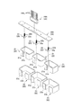
図1から図3の符号1は、本実施形態のコネクタ装置を示す。このコネクタ装置1は、2つの接続対象機器(第1接続対象機器100、第2接続対象機器200)の間に配置され(図2)、その間を電気的に接続させるものである。例えば、コネクタ装置1は、駆動源としての回転機を備えた車両(電気自動車やハイブリッド車等)に搭載される場合、第1接続対象機器100としてのインバータと第2接続対象機器200としての回転機との間に配置される。第1接続対象機器100は、3相交流回路の相毎に端子(以下、「第1相手方端子」という。)101を備えている。また、第2接続対象機器200は、3相交流回路の相毎に端子(以下、「第2相手方端子」という。)201を備えている。
Reference numeral 1 in FIGS. 1 to 3 represents the connector device of the present embodiment. The connector device 1 is arranged between two connection target devices (first
コネクタ装置1は、接続端子10と電流センサ20と筐体30とを備える(図1から図3)。このコネクタ装置1においては、接続端子10と電流センサ20とが対になって筐体30に収容されている。また、このコネクタ装置1においては、一対の接続端子10と電流センサ20が少なくとも1組設けられている。例えば、複数の接続端子10を有する交流回路においては、その接続端子10毎に電流センサ20が設けられている。この例示のコネクタ装置1においては、第1接続対象機器100と第2接続対象機器200における3相交流回路の相毎に、一対の接続端子10と電流センサ20が設けられている。
The connector device 1 includes a
接続端子10は、第1接続対象機器100と第2接続対象機器200の同相同士を電気的に接続させるものである。この接続端子10は、第1接続対象機器100の第1相手方端子101に対して電気的に接続される第1端子接続部10aと、第2接続対象機器200の第2相手方端子201に対して電気的に接続される第2端子接続部10bと、を有している(図1、図3及び図4)。この例示の第1端子接続部10aは、筐体30から突出させた状態で配置されており、第1相手方端子101に対して螺子止めで固定される。一方、この例示の第2端子接続部10bは、第2相手方端子201に対して嵌合固定される。ここでは、第2端子接続部10bを雌端子形状に形成し、かつ、第2相手方端子201を雄端子形状(具体的には雄タブ形状)に形成している。
The
また、接続端子10は、第1端子接続部10aと第2端子接続部10bとの間に配置され、その間を電気的に接続する平板状の連結部10cを有している(図1、図3及び図4)。
Moreover, the
この接続端子10は、1つの導電部材で成形されたものであってもよく、複数の導電部材を組み付けることで形成されたものであってもよい。この例示の接続端子10は、第1端子接続部10aを有する第1端子金具11と、第2端子接続部10b及び連結部10cを有する第2端子金具12と、第1端子金具11及び第2端子金具12を連結させる電線13と、を備えている(図1、図3及び図4)。第1端子金具11は、電線13の一端に対して物理的且つ電気的に接続される電線接続部11aを有している。その電線接続部11aは、電線13の一端に対して加締め等で圧着固定される。第2端子金具12は、電線13の他端に対して物理的且つ電気的に接続される電線接続部12aを有している。その電線接続部12aは、電線13の他端に対して加締め等で圧着固定される。第2端子金具12においては、第2端子接続部10bと電線接続部12aとの間に連結部10cが配置されている。この例示の連結部10cは、第2端子接続部10bと第2相手方端子201との間の挿抜方向に沿う平面を有している。電線13は、第1相手方端子101と第2相手方端子201との間における接続端子10の芯出しのために設けられている。
This
電流センサ20は、接続端子10に流れる電流を測定するものである。この電流センサ20は、連結部10cに流れる電流を当該電流に応じた磁束に基づいて測定する。この電流センサ20は、磁気コア部材21と磁気センサ22と磁気シールド部材23とを備えている(図3、図5及び図6)。また、この電流センサ20は、信号出力器24を備えている(図1から図6)。
The
磁気コア部材21は、連結部10cに流れる電流に応じた磁束を発生させる部材であり、フェライト等の磁性材料で成形される。この磁気コア部材21は、コア主体21aを有する(図3、図5及び図6)。コア主体21aとは、連結部10cを内方で間隔を空けて囲う筒体が主たる形状となり、その筒体に対して筒軸方向に沿うスリット状のギャップ部21bが形成されたものである。この例示のコア主体21aは、角筒状の筒体における4つの壁の内の1つにギャップ部21bを設けている。ギャップ部21bは、その壁の中間部分において、矩形状に形成されている。
The
磁気コア部材21においては、コア主体21aの内方に連結部10cを筒軸方向に沿って挿通させ、かつ、そのコア主体21aの内方で連結部10cをギャップ部21bに対して対向配置させる。ここでは、連結部10cにおける一方の平面をギャップ部21bに対向配置させている。連結部10cにおいては、ギャップ部21bに対して対向配置されている部分が電流の測定対象の部位(以下、「電流測定対象部」という。)となる。
In the
磁気センサ22は、ギャップ部21bにおける磁束密度に応じた信号を出力させるものである。この磁気センサ22は、磁気検出素子を有するセンサ本体22aと、信号の出力を担う導電性のリード線22bと、を備える(図3及び図6)。
The
この例示では、磁気センサ22としてホールIC(Integrated Circuit)を用いる。ホールICは、図示しないが、磁気検出素子としてのホール素子と、このホール素子の出力信号を増幅させるアンプ回路と、を備える。センサ本体22aは、そのホール素子とアンプ回路を内包している。ホール素子は、磁束密度に応じたホール電圧の信号(出力信号)を出力する。例えば、このホール素子は、連結部10cの電流測定対象部の幅方向における略中央から連結部10cの平面に対する直交方向へと所定の間隔を空けた位置に設ける。ここでは、そのようなホール素子の配置が為されるように、ギャップ部21bに磁気センサ22のセンサ本体22aを配置している。この磁気センサ22においては、ギャップ部21bの磁束密度に応じたホール電圧の信号をホール素子が出力し、その出力信号をアンプ回路で増幅する。この磁気センサ22においては、その増幅された出力信号をリード線22bから出力する。
In this example, a Hall IC (Integrated Circuit) is used as the
磁気シールド部材23は、磁気コア部材21のコア主体21aを外方側から囲うシールド主体23aを有するものであり(図3、図5及び図6)、そのシールド主体23aでシールド主体23aの内方と外方との間における磁気を遮蔽する。この磁気シールド部材23は、フェライト等の磁性材料で成形される。シールド主体23aは、コア主体21aを外方側から囲う筒体が主たる形状となるものであり、筒軸方向をコア主体21aの筒軸方向に合わせて配置される。この例示のシールド主体23aは、角筒状の筒体における4つの壁の内の1つに、筒軸方向に沿うスリット状のギャップ部23bが形成されている。ギャップ部23bは、その壁の中間部分で矩形状に形成されており、磁気コア部材21のギャップ部21bに対して、コア主体21aの外方側で間隔を空けて対向配置されている。
The
この電流センサ20においては、磁気コア部材21と磁気センサ22と磁気シールド部材23とが筐体30の後述する第2収容部30bの内方に配置されている。
In the
信号出力器24は、磁気センサ22からの出力信号に基づく電流の測定信号を電子制御装置等の外部機器(図示略)に送信するものである。この信号出力器24は、磁気センサ22のリード線22bからの出力信号が入力される回路基板24Aを備えている(図3、図5及び図6)。その回路基板24Aの回路パターン(図示略)には、リード線22bが電気的に接続されている。また、信号出力器24は、その回路パターンに対して電気的に接続される信号伝達具24Bを備えている(図3、図5及び図6)。その信号伝達具24Bは、外部機器に対して電気的に接続されており、磁気センサ22からの出力信号に基づく電流の測定信号を外部機器に向けて送信する。この例示の信号伝達具24Bは、電線24B1を備えており、この電線24B1を介して外部機器に電流の測定信号を送信する。
The
この信号出力器24は、筐体30の後述する第2収容部30bの内方から外方に渡って配置する。具体的に、信号出力器24は、その第2収容部30bを成す壁体の外壁面の内の筐体30の後述する第1収容部30a側とは別の外壁面から外方に向けて突出させる。信号出力器24においては、回路基板24Aが第2収容部30bの内方に配置され、信号伝達具24Bが第2収容部30bの内方から外方に渡って配置されている。信号伝達具24Bにおいては、電線24B1を第2収容部30bの外方に配置している。
The
筐体30は、合成樹脂等の絶縁性材料で成形する。この筐体30は、先に示したように、接続端子10と電流センサ20とが対になって収容されるものであり、その一対の接続端子10と電流センサ20を3組収容する。この筐体30は、接続端子10の第2端子接続部10bを収容する第1収容部30aと、接続端子10の連結部10c及び電流センサ20を収容する第2収容部30bと、を有している(図1から図3)。
The
第1収容部30aは、筒状に形成して、接続端子10毎に設けている。この第1収容部30aは、第2端子接続部10bが収容され且つ保持される内部空間30a1を有している(図3)。第2端子接続部10bは、内部空間30a1の収容完了位置まで筒軸方向に沿って挿入される。この第2端子接続部10bは、内部空間30a1の収容完了位置まで挿入された際に、この内部空間30a1に設けたランス30a2によって、挿入方向とは逆向きの動きが係止される。第1収容部30aは、筒軸方向における一端に、内部空間30a1に連通する開口部30a3を有している(図3)。その開口部30a3は、第2相手方端子201の挿入口として利用される。それぞれの第1収容部30aは、その開口部30a3の向きを互いに合わせ、かつ、互いに間隔を空けて一列に並べている。
The 1st
第2収容部30bは、全ての接続端子10の連結部10cと電流センサ20の組み合わせを一纏めに収容するべく、筒状に形成する。この第2収容部30bは、全ての接続端子10の連結部10cと電流センサ20の組み合わせが一纏めに収容される内部空間30b1を有している(図1及び図3)。この例示の内部空間30b1には、筒状の端子収容部30b2が連結部10c毎に設けられている。その端子収容部30b2は、該当する第1収容部30aの内部空間30a1に連通させた内部空間30b21を有しており、該当する第1収容部30aに対して、互いの筒軸方向を合わせた状態で連接させている。端子収容部30b2は、その筒軸方向における一端を第1収容部30aの筒軸方向における他端に連通させている。電流センサ20は、この端子収容部30b2を囲うように配置し、充填したポッティング液の硬化体によって第2収容部30bに保持される。
The 2nd
具体的に、この例示の筐体30は、ハウジング31とカバー32とを備えている(図1から図3)。
Specifically, the illustrated
ハウジング31は、第1収容部30aと第2収容部30bとを有する。このハウジング31は、第2収容部30bの筒軸方向における他端に開口部31aを有している(図3)。その開口部31aは、第1収容部30aの開口部30a3とは逆側に配置されており、電流センサ20の挿入口として利用される。信号伝達具24Bは、この開口部31aから第2収容部30bの外方に向けて突出させている。また、このハウジング31は、端子収容部30b2の筒軸方向における他端に開口部31bを有している(図3)。その開口部31bは、第1収容部30aの開口部30a3とは逆側に配置されており、接続端子10の挿入口として利用される。
The
カバー32は、ハウジング31の開口部31aを塞ぎつつ、それぞれの接続端子10における第1端子金具11の電線接続部11aと電線13とを収容する。このカバー32は、その電線接続部11aと電線13とを収容する接続端子10毎の端子収容部32aと、それぞれの端子収容部32aの周縁に設けた鍔部32bと、を有している(図1から図3)。
The
この例示のカバー32は、第1カバー部材32Aと第2カバー部材32Bとを備えている(図1から図3)。第1カバー部材32Aと第2カバー部材32Bは、それぞれの接続端子10の電線接続部11aと電線13を挟み込むように嵌め合わせて、ハウジング31に取り付ける。
The illustrated
この例示の筐体30においては、カバー32の鍔部32bについても第2収容部30bを成す壁体となる。この例示の信号出力器24は、その鍔部32bの外壁面から外方に向けて突出させる。そこで、鍔部32bには、信号出力器24の信号伝達具24Bを挿通させるための切欠き部32b1が形成されている(図1から図3)。信号伝達具24Bは、その切欠き部32b1を介して、第2収容部30bの内方から外方に渡って配置される。
In the illustrated
尚、この筐体30には、ハウジング31を鍔状に囲う板部材33が設けられている(図1から図3)。
The
ここまで説明したように、本実施形態のコネクタ装置1は、接続端子10の第1端子接続部10aや第2端子接続部10bを電流の測定対象としていないので、第1相手方端子101や第2相手方端子201との接続状態を考慮した上で電流センサを配置する必要がない。故に、このコネクタ装置1は、かかる部位での自らの体格の大型化を抑えることができ、かつ、第1接続対象機器100や第2接続対象機器200の体格の大型化をも抑えることができる。一方、本実施形態のコネクタ装置1は、接続端子10の連結部10cを電流の測定対象としているので、かかる部位での自らの体格の大型化を招く虞があるが、その連結部10cを平板状に形成した上で電流センサ20を配置している。例えば、その電流センサ20は、その平板状の連結部10cを囲うように配置している。故に、このコネクタ装置1は、第1端子接続部10aや第2端子接続部10bを電流の測定対象とした場合と比較して、電流センサ20の小型化を図れるので、自らの体格の大型化を可能な限り抑えることができる。そして、このコネクタ装置1は、第1接続対象機器100や第2接続対象機器200の形状如何で、これらの体格の大型化に与える影響を減らすことができる。以上示したように、本実施形態のコネクタ装置1は、自らと相手方(第1接続対象機器100、第2接続対象機器200)の体格の大型化を抑えつつ電流センサ20を備えることができる。
As described so far, the connector device 1 according to the present embodiment does not measure the first
更に、本実施形態のコネクタ装置1は、電流センサ20の信号出力器24を第1端子接続部10aや第2端子接続部10bの第1相手方端子101や第2相手方端子201との接続と関わらない場所に設けた上で、筐体30の外方に信号伝達具24Bを引き出している。故に、このコネクタ装置1は、この点からも、自らと相手方(第1接続対象機器100、第2接続対象機器200)の体格の大型化を抑えることができる。
Furthermore, the connector device 1 of the present embodiment relates to the connection of the
また、本実施形態のコネクタ装置1は、信号出力器24に至るまでの電流センサ20の全ての構成を包含しているので、互いに嵌合される2つのコネクタ間に電流センサが分散配置されたものと比して、部品点数を減らすことができるので、原価の低減が可能になる。
Moreover, since the connector apparatus 1 of this embodiment includes all the structures of the
1 コネクタ装置
10 接続端子
10a 第1端子接続部
10b 第2端子接続部
10c 連結部
20 電流センサ
21 磁気コア部材
21a コア主体
21b ギャップ部
22 磁気センサ
23 磁気シールド部材
23a シールド主体
24 信号出力器
30 筐体
30a 第1収容部
30b 第2収容部
101 第1相手方端子
201 第2相手方端子
DESCRIPTION OF SYMBOLS 1
Claims (4)
前記連結部に流れる電流を当該電流に応じた磁束に基づいて測定する電流センサと、
前記第2端子接続部を収容する第1収容部並びに前記連結部及び前記電流センサを収容する第2収容部を有する筐体と、
を備えることを特徴としたコネクタ装置。 A first terminal connection portion electrically connected to the first counterpart terminal, a second terminal connection portion electrically connected to the second counterpart terminal, and the first terminal connection portion and the second A connecting terminal having a flat plate-like connecting portion that is arranged between the terminal connecting portion and electrically connecting the terminal connecting portion;
A current sensor for measuring a current flowing through the connecting portion based on a magnetic flux corresponding to the current;
A housing having a first housing portion for housing the second terminal connection portion and a second housing portion for housing the coupling portion and the current sensor;
A connector device comprising:
前記信号出力器は、前記第2収容部を成す壁体の外壁面の内の前記第1収容部側とは別の外壁面から外方に向けて突出させることを特徴とした請求項1に記載のコネクタ装置。 The current sensor includes a signal output device that transmits a current measurement signal to an external device;
The said signal output device protrudes outward from the outer wall surface different from the said 1st accommodating part side in the outer wall surface of the wall body which comprises the said 2nd accommodating part. The connector device as described.
前記信号出力器は、前記第2収容部を成す壁体の外壁面の内の前記第1収容部側とは別の外壁面から外方に向けて突出させることを特徴とした請求項1に記載のコネクタ装置。 The current sensor has a core main body in which a slit-like gap portion is formed along a cylindrical axis direction with respect to a cylindrical body that surrounds the connecting portion with an interval therebetween, and corresponds to a current flowing through the connecting portion. A magnetic core member that generates a magnetic flux, a magnetic sensor that outputs a signal according to the magnetic flux density in the gap portion, and a shield main body that surrounds the core main body from the outside, and the shield main body and the shield main body A magnetic shield member that shields magnetism between the inner side and the outer side is disposed inside the second housing portion, and a current measurement signal based on an output signal from the magnetic sensor is transmitted to an external device. A signal output device is arranged from the inside of the second housing part to the outside,
The said signal output device protrudes outward from the outer wall surface different from the said 1st accommodating part side in the outer wall surface of the wall body which comprises the said 2nd accommodating part. The connector device as described.
Priority Applications (4)
| Application Number | Priority Date | Filing Date | Title |
|---|---|---|---|
| JP2017105281A JP2018200823A (en) | 2017-05-29 | 2017-05-29 | Connector device |
| US15/909,648 US10446987B2 (en) | 2017-05-29 | 2018-03-01 | Connector device |
| DE102018206240.4A DE102018206240A1 (en) | 2017-05-29 | 2018-04-24 | connector device |
| CN201810494851.4A CN108933371A (en) | 2017-05-29 | 2018-05-22 | Electrical connector |
Applications Claiming Priority (1)
| Application Number | Priority Date | Filing Date | Title |
|---|---|---|---|
| JP2017105281A JP2018200823A (en) | 2017-05-29 | 2017-05-29 | Connector device |
Publications (1)
| Publication Number | Publication Date |
|---|---|
| JP2018200823A true JP2018200823A (en) | 2018-12-20 |
Family
ID=64109360
Family Applications (1)
| Application Number | Title | Priority Date | Filing Date |
|---|---|---|---|
| JP2017105281A Abandoned JP2018200823A (en) | 2017-05-29 | 2017-05-29 | Connector device |
Country Status (4)
| Country | Link |
|---|---|
| US (1) | US10446987B2 (en) |
| JP (1) | JP2018200823A (en) |
| CN (1) | CN108933371A (en) |
| DE (1) | DE102018206240A1 (en) |
Cited By (1)
| Publication number | Priority date | Publication date | Assignee | Title |
|---|---|---|---|---|
| WO2022138014A1 (en) * | 2020-12-21 | 2022-06-30 | 株式会社オートネットワーク技術研究所 | Terminal block |
Families Citing this family (7)
| Publication number | Priority date | Publication date | Assignee | Title |
|---|---|---|---|---|
| JP2018200823A (en) * | 2017-05-29 | 2018-12-20 | 矢崎総業株式会社 | Connector device |
| JP6811229B2 (en) * | 2018-12-28 | 2021-01-13 | 矢崎総業株式会社 | connector |
| CN114094403B (en) * | 2019-08-09 | 2024-06-14 | 华为数字能源技术有限公司 | Filtering connection device and filtering method |
| DE102020100635A1 (en) * | 2020-01-14 | 2021-07-15 | Schaeffler Technologies AG & Co. KG | High-voltage connection module and converter |
| US11349265B2 (en) * | 2020-09-14 | 2022-05-31 | Infineon Technologies Ag | Magnetic current sensor integration into high current connector device |
| CN218343420U (en) * | 2022-09-21 | 2023-01-20 | 长春捷翼汽车零部件有限公司 | Electrical connector |
| WO2024083326A1 (en) * | 2022-10-19 | 2024-04-25 | Gkn Automotive Limited | Busbar arrangement, and arrangement |
Citations (6)
| Publication number | Priority date | Publication date | Assignee | Title |
|---|---|---|---|---|
| JP2008224260A (en) * | 2007-03-09 | 2008-09-25 | Tamura Seisakusho Co Ltd | Electric current detector |
| JP2013020822A (en) * | 2011-07-12 | 2013-01-31 | Denso Corp | Connector with built-in sensor and connection structure thereof |
| US20130214593A1 (en) * | 2012-02-22 | 2013-08-22 | Sumitomo Electric Industries, Ltd. | Relay busbar device with built-in current sensor for vehicle |
| WO2013136751A1 (en) * | 2012-03-16 | 2013-09-19 | キヤノン電子株式会社 | Measurement module, electronic apparatus, power source tap, power source unit, and embedded measurement module |
| JP2013196861A (en) * | 2012-03-16 | 2013-09-30 | Canon Electronics Inc | Ac inlet, current detection device, voltage detection device, electronic equipment, and power supply tap |
| JP2015201401A (en) * | 2014-04-10 | 2015-11-12 | 日立金属株式会社 | connector device |
Family Cites Families (9)
| Publication number | Priority date | Publication date | Assignee | Title |
|---|---|---|---|---|
| JP5414333B2 (en) * | 2009-04-09 | 2014-02-12 | 矢崎総業株式会社 | Current detector assembly structure |
| JP5435825B2 (en) * | 2012-01-05 | 2014-03-05 | 日本航空電子工業株式会社 | Connector and connector assembly |
| FR2998059B1 (en) * | 2012-11-15 | 2014-12-19 | Schneider Electric Ind Sas | MIXED CURRENT SENSOR AND METHOD OF MOUNTING SAME |
| EP3026445B1 (en) * | 2014-11-28 | 2017-08-23 | LEM Intellectual Property SA | Electrical current transducer with electrostatic shield |
| US20170102606A1 (en) * | 2016-12-21 | 2017-04-13 | Mohawk Innovations Limited | Modular Sensing Device |
| US10422821B2 (en) * | 2017-04-17 | 2019-09-24 | Rockwell Automation Technologies, Inc. | System and method of identifying a module in a stack light |
| JP6596033B2 (en) * | 2017-05-08 | 2019-10-23 | 矢崎総業株式会社 | Current sensor |
| JP2018189504A (en) * | 2017-05-08 | 2018-11-29 | 矢崎総業株式会社 | Curent sensor |
| JP2018200823A (en) * | 2017-05-29 | 2018-12-20 | 矢崎総業株式会社 | Connector device |
-
2017
- 2017-05-29 JP JP2017105281A patent/JP2018200823A/en not_active Abandoned
-
2018
- 2018-03-01 US US15/909,648 patent/US10446987B2/en active Active
- 2018-04-24 DE DE102018206240.4A patent/DE102018206240A1/en not_active Withdrawn
- 2018-05-22 CN CN201810494851.4A patent/CN108933371A/en active Pending
Patent Citations (8)
| Publication number | Priority date | Publication date | Assignee | Title |
|---|---|---|---|---|
| JP2008224260A (en) * | 2007-03-09 | 2008-09-25 | Tamura Seisakusho Co Ltd | Electric current detector |
| JP2013020822A (en) * | 2011-07-12 | 2013-01-31 | Denso Corp | Connector with built-in sensor and connection structure thereof |
| US20130214593A1 (en) * | 2012-02-22 | 2013-08-22 | Sumitomo Electric Industries, Ltd. | Relay busbar device with built-in current sensor for vehicle |
| JP2013170984A (en) * | 2012-02-22 | 2013-09-02 | Sumitomo Electric Ind Ltd | Relay bus bar apparatus with current sensor for use in vehicle |
| WO2013136751A1 (en) * | 2012-03-16 | 2013-09-19 | キヤノン電子株式会社 | Measurement module, electronic apparatus, power source tap, power source unit, and embedded measurement module |
| JP2013196861A (en) * | 2012-03-16 | 2013-09-30 | Canon Electronics Inc | Ac inlet, current detection device, voltage detection device, electronic equipment, and power supply tap |
| US20140375305A1 (en) * | 2012-03-16 | 2014-12-25 | Canon Denshi Kabushiki Kaisha | Measurement module, electronic apparatus, power supply tap, power supply unit, and built-in measurement module |
| JP2015201401A (en) * | 2014-04-10 | 2015-11-12 | 日立金属株式会社 | connector device |
Cited By (3)
| Publication number | Priority date | Publication date | Assignee | Title |
|---|---|---|---|---|
| WO2022138014A1 (en) * | 2020-12-21 | 2022-06-30 | 株式会社オートネットワーク技術研究所 | Terminal block |
| JP2022098336A (en) * | 2020-12-21 | 2022-07-01 | 株式会社オートネットワーク技術研究所 | Terminal block |
| JP7501346B2 (en) | 2020-12-21 | 2024-06-18 | 株式会社オートネットワーク技術研究所 | Terminal block |
Also Published As
| Publication number | Publication date |
|---|---|
| US20180342841A1 (en) | 2018-11-29 |
| CN108933371A (en) | 2018-12-04 |
| US10446987B2 (en) | 2019-10-15 |
| DE102018206240A1 (en) | 2018-11-29 |
Similar Documents
| Publication | Publication Date | Title |
|---|---|---|
| JP2018200823A (en) | Connector device | |
| JP6830986B2 (en) | Current converter | |
| KR102475347B1 (en) | Current Transducer with Integrated Primary Conductor Bar | |
| JP4796060B2 (en) | Current sensor | |
| JP5098855B2 (en) | Current sensor | |
| JP6302453B2 (en) | Current sensor | |
| JP4814283B2 (en) | Current sensor | |
| TWI495880B (en) | Probe module | |
| JP2018189504A (en) | Curent sensor | |
| JP2010127896A (en) | Current detector | |
| JP2016506618A (en) | Non-contact connector | |
| JP2018191452A (en) | Electrical connection box | |
| JP2012047564A (en) | Current detection apparatus | |
| WO2012144454A1 (en) | Connector and detecting device using same | |
| JP2013231691A (en) | Current sensor | |
| CN116007807A (en) | Electromagnetic ultrasonic sensor | |
| EP3764107B1 (en) | Current transducer for measuring residual currents | |
| US11994538B2 (en) | Current transducer with magnetic core on primary conductor bar | |
| JP6419432B2 (en) | Current detection device using magnetic core for current detection | |
| CN109839520B (en) | Measuring device for an electrical switching device | |
| JP2013217866A (en) | Electrical junction box and current sensor | |
| JP2012058199A (en) | Current detection apparatus | |
| JP2020128935A (en) | Current sensor and service plug | |
| JP2017017958A (en) | Current sensor and distribution board having the same | |
| JP2017195227A (en) | Standard resistor |
Legal Events
| Date | Code | Title | Description |
|---|---|---|---|
| A621 | Written request for application examination |
Free format text: JAPANESE INTERMEDIATE CODE: A621 Effective date: 20180810 |
|
| A977 | Report on retrieval |
Free format text: JAPANESE INTERMEDIATE CODE: A971007 Effective date: 20190404 |
|
| A131 | Notification of reasons for refusal |
Free format text: JAPANESE INTERMEDIATE CODE: A131 Effective date: 20190416 |
|
| A521 | Request for written amendment filed |
Free format text: JAPANESE INTERMEDIATE CODE: A523 Effective date: 20190527 |
|
| A131 | Notification of reasons for refusal |
Free format text: JAPANESE INTERMEDIATE CODE: A131 Effective date: 20190903 |
|
| A762 | Written abandonment of application |
Free format text: JAPANESE INTERMEDIATE CODE: A762 Effective date: 20191105 |