JP2018190838A - diode - Google Patents
diode Download PDFInfo
- Publication number
- JP2018190838A JP2018190838A JP2017092463A JP2017092463A JP2018190838A JP 2018190838 A JP2018190838 A JP 2018190838A JP 2017092463 A JP2017092463 A JP 2017092463A JP 2017092463 A JP2017092463 A JP 2017092463A JP 2018190838 A JP2018190838 A JP 2018190838A
- Authority
- JP
- Japan
- Prior art keywords
- region
- anode
- diode
- barrier
- type
- Prior art date
- Legal status (The legal status is an assumption and is not a legal conclusion. Google has not performed a legal analysis and makes no representation as to the accuracy of the status listed.)
- Pending
Links
Images


Landscapes
- Metal-Oxide And Bipolar Metal-Oxide Semiconductor Integrated Circuits (AREA)
Abstract
Description
本明細書に開示の技術は、ダイオードに関する。 The technology disclosed in this specification relates to a diode.
特許文献1には、バリア領域とピラー領域を有するダイオードが開示されている。バリア領域は、n型領域であり、アノード領域(アノード電極に接するp型領域)とn型ドリフト領域の間に配置されている。ピラー領域は、n型領域であり、アノード電極に接しているとともに、バリア領域に接続されている。このダイオードでは、順方向電圧を上昇させるときに、ピラー領域とバリア領域を介してバイパス電流が流れることで、アノード領域とバリア領域の界面のpn接合に印加される電圧が上昇し難くなっている。このため、アノード領域からドリフト領域へホールが注入され難い。このため、このダイオードがリカバリ動作を行うときに、アノード電極へ排出されるホールが少ない。したがって、このダイオードには、リカバリ電流が流れ難い。 Patent Document 1 discloses a diode having a barrier region and a pillar region. The barrier region is an n-type region, and is disposed between the anode region (p-type region in contact with the anode electrode) and the n-type drift region. The pillar region is an n-type region, is in contact with the anode electrode, and is connected to the barrier region. In this diode, when the forward voltage is increased, a bypass current flows through the pillar region and the barrier region, so that the voltage applied to the pn junction at the interface between the anode region and the barrier region is difficult to increase. . For this reason, it is difficult for holes to be injected from the anode region to the drift region. For this reason, when this diode performs a recovery operation, there are few holes discharged to the anode electrode. Therefore, it is difficult for a recovery current to flow through this diode.
特許文献1に記載されているように、バリア領域とピラー領域を有するダイオードでは、スナップバック現象が発生する場合がある。つまり、順方向電圧を上昇させるときに、バイパス電流が過度に流れて、pn接合への印加電圧の上昇が過度に抑制される。その結果、順方向電圧が想定値より高い値まで上昇した段階でpn接合がオンする。pn接合がオンすると、電流が増加しながら順方向電圧が一旦低下する。このようなスナップバック現象が生じると、ダイオードで生じる損失が増加する。特許文献1のダイオードは、バリア領域の不純物濃度を位置によって変化させることで、スナップバック現象を抑制する。 As described in Patent Document 1, a snapback phenomenon may occur in a diode having a barrier region and a pillar region. That is, when the forward voltage is increased, the bypass current flows excessively, and the increase of the voltage applied to the pn junction is excessively suppressed. As a result, the pn junction is turned on when the forward voltage rises to a value higher than the assumed value. When the pn junction is turned on, the forward voltage once decreases while the current increases. When such a snapback phenomenon occurs, the loss generated in the diode increases. The diode of Patent Document 1 suppresses the snapback phenomenon by changing the impurity concentration of the barrier region depending on the position.
特許文献1の技術とは別の構成で、スナップバック現象を抑制する技術を提案する。 A technique for suppressing the snapback phenomenon with a configuration different from the technique of Patent Document 1 is proposed.
本明細書が開示するダイオードは、半導体基板と、前記半導体基板に接するアノード電極を有する。前記半導体基板が、前記アノード電極に接するp型のアノード領域と、前記アノード領域に接するn型のバリア領域と、前記バリア領域によって前記アノード領域から分離されているとともに前記バリア領域よりも低いn型不純物濃度を有するn型のドリフト領域と、前記アノード電極に接するとともに前記アノード領域によって前記バリア領域から分離されているn型のピラー領域を有する。前記アノード領域の前記ピラー領域と前記バリア領域の間に位置する部分のp型不純物濃度のピーク値が、前記バリア領域のn型不純物濃度のピーク値よりも高い。 The diode disclosed in this specification includes a semiconductor substrate and an anode electrode in contact with the semiconductor substrate. The semiconductor substrate is separated from the anode region by the p-type anode region in contact with the anode electrode, the n-type barrier region in contact with the anode region, and the barrier region, and is lower than the barrier region. An n-type drift region having an impurity concentration; and an n-type pillar region in contact with the anode electrode and separated from the barrier region by the anode region. The peak value of the p-type impurity concentration in the portion located between the pillar region and the barrier region in the anode region is higher than the peak value of the n-type impurity concentration in the barrier region.
なお、ドリフト領域とバリア領域が互いに接していてもよいし、ドリフト領域とバリア領域の間にp型領域が配置されていてもよい。 Note that the drift region and the barrier region may be in contact with each other, or a p-type region may be disposed between the drift region and the barrier region.
この構成では、ピラー領域がアノード領域によってバリア領域から分離されているとともに、アノード領域のピラー領域とバリア領域の間に位置する部分のp型不純物濃度のピーク値がバリア領域のn型不純物濃度のピーク値よりも高い。このため、ダイオードに順方向電圧を印加するときに、ピラー領域とバリア領域を介して流れるバイパス電流を抑制することができる。したがって、アノード領域とバリア領域の界面のpn接合に印加される電圧の上昇が過度に抑制されることを防止できる。したがって、この構成によれば、スナップバック現象を抑制することができる。 In this configuration, the pillar region is separated from the barrier region by the anode region, and the peak value of the p-type impurity concentration in the portion located between the pillar region and the barrier region in the anode region is equal to the n-type impurity concentration in the barrier region. Higher than the peak value. For this reason, when a forward voltage is applied to the diode, a bypass current flowing through the pillar region and the barrier region can be suppressed. Therefore, it is possible to prevent an excessive increase in the voltage applied to the pn junction at the interface between the anode region and the barrier region. Therefore, according to this configuration, the snapback phenomenon can be suppressed.
なお、本明細書に開示の構成を、特許文献1の構成と組み合わせることでスナップバック現象を抑制してもよい。 Note that the snapback phenomenon may be suppressed by combining the configuration disclosed in this specification with the configuration of Patent Document 1.
図1に示す実施形態のダイオード10は、半導体基板12と、アノード電極14と、カソード電極16を有している。半導体基板12は、シリコンを主成分とする基板である。アノード電極14は、半導体基板12の上面に接している。カソード電極16は、半導体基板12の下面に接している。
The
半導体基板12は、アノード領域20、ピラー領域22、バリア領域24、ドリフト領域26、バッファ領域28及びカソード領域30を有している。
The
アノード領域20は、p型領域であり、アノード電極14に接する範囲に配置されている。アノード領域20は、コンタクト領域20aと、コンタクト領域20aよりもp型不純物濃度が低い低濃度領域20bを有している。コンタクト領域20aは、アノード電極14に対してオーミック接触している。低濃度領域20bは、コンタクト領域20aの周囲に配置されている。低濃度領域20bは、コンタクト領域20aとピラー領域22の下部まで分布している。低濃度領域20bは、コンタクト領域20aに隣接する位置でアノード電極14に接している。
The
ピラー領域22は、n型領域であり、アノード電極14に接する範囲に配置されている。ピラー領域22は、アノード電極14に対してショットキー接触している。但し、ピラー領域22は、アノード電極14に対してオーミック接触していてもよい。ピラー領域22は、アノード電極14に接する位置から下方向に長く伸びている。ピラー領域22は、コンタクト領域20aの下端よりも深い位置まで伸びている。ピラー領域22は、低濃度領域20bに接している。
The
バリア領域24は、n型領域であり、アノード領域20の下側に配置されている。バリア領域24は、低濃度領域20bに対して下側から接している。バリア領域24とピラー領域22の間には低濃度領域20bが分布している。バリア領域24は、低濃度領域20bによってピラー領域22から分離されている。
The
ドリフト領域26は、バリア領域24よりもn型不純物濃度が低いn型領域である。ドリフト領域26は、バリア領域24に対して下側から接している。ドリフト領域26は、バリア領域24によってアノード領域20から分離されている。
The
バッファ領域28は、ドリフト領域26よりもn型不純物濃度が高いn型領域である。バッファ領域28は、ドリフト領域26に対して下側から接している。バッファ領域28は、ドリフト領域26によってバリア領域24から分離されている。
The
カソード領域30は、バッファ領域28よりもn型不純物濃度が高いn型領域である。カソード領域30は、バッファ領域28に対して下側から接している。カソード領域30は、バッファ領域28によってドリフト領域26から分離されている。
The
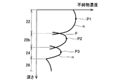
図2は、図1のII−II線に沿って測定した不純物濃度分布を示している。すなわち、図2は、半導体基板12の厚み方向に沿ってピラー領域22、低濃度領域20b、バリア領域24及びドリフト領域26を横切る範囲の不純物濃度分布を示している。図2に示すように、ピラー領域22内でn型不純物濃度がピーク値P1を有するように分布しており、低濃度領域20b内でp型不純物濃度がピーク値P2を有するように分布しており、バリア領域24内でn型不純物濃度がピーク値P3を有するように分布している。ピーク値P1はピーク値P2よりも大きい。また、ピーク値P2はピーク値P3よりも大きい。
FIG. 2 shows an impurity concentration distribution measured along the line II-II in FIG. That is, FIG. 2 shows an impurity concentration distribution in a range that crosses the
次に、ダイオード10の動作について説明する。ダイオード10に印加する電圧(アノード電極14のカソード電極16に対する電位)を徐々に上昇させると、図1の矢印に示すように電子が流れる。すなわち、電子が、カソード電極16からアノード電極14へカソード領域30、バッファ領域28、ドリフト領域26、バリア領域24及びピラー領域22を経由して流れる。このため、図1の矢印の逆向きに、バイパス電流が流れる。なお、バリア領域24とピラー領域22の間にp型の低濃度領域20bが存在するが、電子は低濃度領域20bを貫通して流れる。このように電子が流れることで、低濃度領域20bとバリア領域24の界面のpn接合50に印加される電圧の上昇が抑制される。なお、バリア領域24とピラー領域22の間にp型の低濃度領域20bが存在するので、矢印に示す電子の経路の抵抗が高く、バイパス電流はそれほど大きくない。特に、バリア領域24とピラー領域22の間に位置する低濃度領域20bのp型不純物濃度のピーク値P2がバリア領域24のn型不純物濃度のピーク値P3よりも高いので、バイパス電流が抑制される。
Next, the operation of the
順方向電圧をさらに上昇させると、低濃度領域20bとバリア領域24の界面のpn接合50に印加される電圧が上昇し、pn接合50がオンする。pn接合50がオンすると、アノード領域20からドリフト領域26にホールが流入して、ドリフト領域26の抵抗が低下する。したがって、低損失で電流がダイオード10内を流れる。すなわち、ダイオード10がオンする。ダイオード10では、上述したようにバイパス電流が流れることで、pn接合50に印加される電圧の上昇が抑制される。このため、ダイオード10では、バイパス電流が流れないダイオードに比べて、ドリフト領域26に流入するホールが少ない。
When the forward voltage is further increased, the voltage applied to the
その後、ダイオード10に印加する電圧を逆方向電圧(アノード電極14がカソード電極16よりも低電位となる電圧)に切り換えると、ダイオード10がリカバリ動作を行う。すなわち、ドリフト領域26内に存在するホールが、アノード領域20を介してアノード電極14に排出される。このため、ダイオード10に瞬間的に逆電流(リカバリ電流)が流れる。しかしながら、上述したように、ダイオード10では、オンしているときにドリフト領域26に流入するホールが少ない。このため、リカバリ動作時にアノード電極14に排出されるホールが少ない。このため、ダイオード10にリカバリ電流が流れ難い。
Thereafter, when the voltage applied to the
図3は、ダイオードがオンするときの電圧Vfと電流Ifの変化を示している。なお、電圧Vfは、アノード電極14のカソード電極16に対する電圧であり、電流Ifはアノード電極14からカソード電極16に流れる電流である。図3の実線は実施形態のダイオード10の特性を示している。図3の破線は、ピラー領域22とバリア領域24が繋がっているダイオードにおいて、スナップバック現象が生じているときの特性を示している。ピラー領域22とバリア領域24が繋がっていると、電圧Vfを上昇させるときに流れるバイパス電流が大きく、pn接合50に印加される電圧が必要以上に上昇し難い場合がある。この場合、電流Ifがほとんど増加せずに電圧Vfが高い値まで上昇する。電圧Vfが所定の値まで上昇すると、pn接合50に印加される電圧がpn接合50をオンさせるのに十分な値に達し、pn接合50がオンする。すると、電圧Vfが急激に低下するとともに電流Ifが増加する。このように、ピラー領域22とバリア領域24が繋がっている場合には、電流Ifがほとんど流れずに電圧Vfが高い値まで上昇し、その後に電圧Vfが急激に低下する現象(すなわち、スナップバック現象)が生じる場合がある。
FIG. 3 shows changes in the voltage Vf and the current If when the diode is turned on. The voltage Vf is a voltage with respect to the
これに対し、本実施形態のダイオード10では、ピラー領域22とバリア領域24が低濃度領域20bによって分離されている。また、ピラー領域22とバリア領域24の間に位置する低濃度領域20bのp型不純物濃度のピーク値P2が、バリア領域24のn型不純物濃度のピーク値P3よりも高い。このため、バイパス電流が抑制され、pn接合50に印加される電圧の上昇が過度に抑制されることがない。したがって、実施形態のダイオード10では、図3の実線のグラフのように、スナップバック現象が生じない。
On the other hand, in the
以上に説明したように、実施形態のダイオード10によれば、ダイオード10のリカバリ電流を抑制できるとともに、スナップバック現象を抑制することができる。
As described above, according to the
なお、上述したダイオード10では、ドリフト領域26がバリア領域24に対して下側から接していた。しかしながら、図4に示すように、バリア領域24とドリフト領域26の間にp型領域60が設けられていてもよい。なお、p型領域60は、電子及びホールが貫通して流れることができるように、濃度及び厚みが調整されている。
In the
また、上述したダイオード10では、カソード電極16に接する範囲全体にカソード領域30が設けられていたが、図5に示すように、カソード電極16に接する範囲にカソード領域30とp型領域62が設けられていてもよい。
In the
また、図6に示すように、半導体基板12の上面にトレンチが設けられており、トレンチ内に絶縁膜70によって半導体基板12から絶縁された電極72が配置されていてもよい。
Further, as shown in FIG. 6, a trench may be provided on the upper surface of the
また、図7に示すように、トレンチ内に電極72を設けた構成において、バリア領域24とドリフト領域26の間にp型領域60が設けられていてもよい。
Further, as shown in FIG. 7, in the configuration in which the
また、図8に示すように、半導体基板12に、ダイオードとして動作するダイオード領域110と、IGBTとして動作するIGBT領域112が設けられていてもよい。ダイオード領域110とIGBT領域112は、トレンチによって区切られている。トレンチ内の電極72は、IGBTのゲートとして用いることができる。IGBT領域112内には、アノード電極14と絶縁膜70に接する範囲にn型のエミッタ領域90が設けられている。また、IGBT領域112内には、カソード領域30に代えてp型のコレクタ領域92が設けられている。コレクタ領域92は、カソード電極16に接している。IGBT領域112内のIGBTが動作するときには、アノード電極14がIGBTのエミッタ電極として機能し、カソード電極16がIGBTのコレクタ電極として機能する。
Further, as shown in FIG. 8, a
以上、実施形態について詳細に説明したが、これらは例示にすぎず、特許請求の範囲を限定するものではない。特許請求の範囲に記載の技術には、以上に例示した具体例をさまざまに変形、変更したものが含まれる。本明細書または図面に説明した技術要素は、単独あるいは各種の組み合わせによって技術有用性を発揮するものであり、出願時請求項記載の組み合わせに限定されるものではない。また、本明細書または図面に例示した技術は複数目的を同時に達成するものであり、そのうちの1つの目的を達成すること自体で技術有用性を持つものである。 The embodiments have been described in detail above, but these are merely examples and do not limit the scope of the claims. The technology described in the claims includes various modifications and changes of the specific examples illustrated above. The technical elements described in this specification or the drawings exhibit technical usefulness alone or in various combinations, and are not limited to the combinations described in the claims at the time of filing. In addition, the technology exemplified in this specification or the drawings achieves a plurality of objects at the same time, and has technical usefulness by achieving one of them.
10 :ダイオード
12 :半導体基板
14 :アノード電極
16 :カソード電極
20 :アノード領域
22 :ピラー領域
24 :バリア領域
26 :ドリフト領域
28 :バッファ領域
30 :カソード領域
50 :pn接合
10: diode 12: semiconductor substrate 14: anode electrode 16: cathode electrode 20: anode region 22: pillar region 24: barrier region 26: drift region 28: buffer region 30: cathode region 50: pn junction
Claims (1)
半導体基板と、
前記半導体基板に接するアノード電極、
を有し、
前記半導体基板が、
前記アノード電極に接するp型のアノード領域と、
前記アノード領域に接するn型のバリア領域と、
前記バリア領域によって前記アノード領域から分離されており、前記バリア領域よりも低いn型不純物濃度を有するn型のドリフト領域と、
前記アノード電極に接し、前記アノード領域によって前記バリア領域から分離されているn型のピラー領域、
を有し、
前記アノード領域の前記ピラー領域と前記バリア領域の間に位置する部分のp型不純物濃度のピーク値が、前記バリア領域のn型不純物濃度のピーク値よりも高い、
ダイオード。 A diode,
A semiconductor substrate;
An anode electrode in contact with the semiconductor substrate;
Have
The semiconductor substrate is
A p-type anode region in contact with the anode electrode;
An n-type barrier region in contact with the anode region;
An n-type drift region separated from the anode region by the barrier region and having an n-type impurity concentration lower than that of the barrier region;
An n-type pillar region in contact with the anode electrode and separated from the barrier region by the anode region;
Have
The peak value of the p-type impurity concentration of the portion located between the pillar region and the barrier region of the anode region is higher than the peak value of the n-type impurity concentration of the barrier region,
diode.
Priority Applications (1)
| Application Number | Priority Date | Filing Date | Title |
|---|---|---|---|
| JP2017092463A JP2018190838A (en) | 2017-05-08 | 2017-05-08 | diode |
Applications Claiming Priority (1)
| Application Number | Priority Date | Filing Date | Title |
|---|---|---|---|
| JP2017092463A JP2018190838A (en) | 2017-05-08 | 2017-05-08 | diode |
Publications (1)
| Publication Number | Publication Date |
|---|---|
| JP2018190838A true JP2018190838A (en) | 2018-11-29 |
Family
ID=64478861
Family Applications (1)
| Application Number | Title | Priority Date | Filing Date |
|---|---|---|---|
| JP2017092463A Pending JP2018190838A (en) | 2017-05-08 | 2017-05-08 | diode |
Country Status (1)
| Country | Link |
|---|---|
| JP (1) | JP2018190838A (en) |
Cited By (1)
| Publication number | Priority date | Publication date | Assignee | Title |
|---|---|---|---|---|
| CN111326576A (en) * | 2020-02-14 | 2020-06-23 | 重庆邮电大学 | SA-LIGBT device with longitudinal separation anode |
Citations (3)
| Publication number | Priority date | Publication date | Assignee | Title |
|---|---|---|---|---|
| JP2008205015A (en) * | 2007-02-16 | 2008-09-04 | Mitsubishi Electric Corp | Semiconductor device and method for manufacturing the same |
| JP2013021240A (en) * | 2011-07-13 | 2013-01-31 | Toyota Central R&D Labs Inc | Diode and semiconductor device |
| JP2014135419A (en) * | 2013-01-11 | 2014-07-24 | Toyota Central R&D Labs Inc | Diode and semiconductor device with built-in diode |
-
2017
- 2017-05-08 JP JP2017092463A patent/JP2018190838A/en active Pending
Patent Citations (3)
| Publication number | Priority date | Publication date | Assignee | Title |
|---|---|---|---|---|
| JP2008205015A (en) * | 2007-02-16 | 2008-09-04 | Mitsubishi Electric Corp | Semiconductor device and method for manufacturing the same |
| JP2013021240A (en) * | 2011-07-13 | 2013-01-31 | Toyota Central R&D Labs Inc | Diode and semiconductor device |
| JP2014135419A (en) * | 2013-01-11 | 2014-07-24 | Toyota Central R&D Labs Inc | Diode and semiconductor device with built-in diode |
Cited By (2)
| Publication number | Priority date | Publication date | Assignee | Title |
|---|---|---|---|---|
| CN111326576A (en) * | 2020-02-14 | 2020-06-23 | 重庆邮电大学 | SA-LIGBT device with longitudinal separation anode |
| CN111326576B (en) * | 2020-02-14 | 2023-03-14 | 重庆邮电大学 | SA-LIGBT device with longitudinal separation anode |
Similar Documents
| Publication | Publication Date | Title |
|---|---|---|
| JP5918288B2 (en) | Semiconductor device | |
| JP6158058B2 (en) | Semiconductor device | |
| US10593668B2 (en) | Semiconductor device and corresponding manufacturing method | |
| US9219060B2 (en) | Semiconductor device | |
| JP6126150B2 (en) | Semiconductor device | |
| JP6053050B2 (en) | Reverse conducting IGBT | |
| JP6222702B2 (en) | Semiconductor device | |
| JP2016032105A (en) | Reverse conducting IGBT | |
| US10304969B2 (en) | Semiconductor device | |
| JP2019054070A (en) | Semiconductor device | |
| US20170110596A1 (en) | Semiconductor device | |
| US10083956B2 (en) | Semiconductor device | |
| JP6077309B2 (en) | Diode and semiconductor device incorporating diode | |
| JP2018125443A (en) | Semiconductor device | |
| JP6799515B2 (en) | Semiconductor device | |
| JPH05226638A (en) | Semiconductor device | |
| JP2018190838A (en) | diode | |
| US9123557B2 (en) | Fast recovery rectifier | |
| JP2019161112A (en) | Semiconductor device | |
| JP6217700B2 (en) | diode | |
| JP6550995B2 (en) | Semiconductor device | |
| US9209287B2 (en) | Power semiconductor device | |
| JP2018519660A (en) | Thyristor with improved plasma spread | |
| JP6852541B2 (en) | Semiconductor device | |
| US20150311334A1 (en) | Semiconductor device |
Legal Events
| Date | Code | Title | Description |
|---|---|---|---|
| A621 | Written request for application examination |
Free format text: JAPANESE INTERMEDIATE CODE: A621 Effective date: 20200303 |
|
| A977 | Report on retrieval |
Free format text: JAPANESE INTERMEDIATE CODE: A971007 Effective date: 20210128 |
|
| A131 | Notification of reasons for refusal |
Free format text: JAPANESE INTERMEDIATE CODE: A131 Effective date: 20210202 |
|
| A02 | Decision of refusal |
Free format text: JAPANESE INTERMEDIATE CODE: A02 Effective date: 20210803 |