JP2018137483A - Plasma processing method and substrate produced using this method - Google Patents
Plasma processing method and substrate produced using this method Download PDFInfo
- Publication number
- JP2018137483A JP2018137483A JP2018098774A JP2018098774A JP2018137483A JP 2018137483 A JP2018137483 A JP 2018137483A JP 2018098774 A JP2018098774 A JP 2018098774A JP 2018098774 A JP2018098774 A JP 2018098774A JP 2018137483 A JP2018137483 A JP 2018137483A
- Authority
- JP
- Japan
- Prior art keywords
- substrate
- etching
- mask
- side mask
- processing method
- Prior art date
- Legal status (The legal status is an assumption and is not a legal conclusion. Google has not performed a legal analysis and makes no representation as to the accuracy of the status listed.)
- Pending
Links
Images


Abstract
Description
本発明は、基板からこの基板よりも小さい基板をプラズマエッチングによって切り出すプラズマ加工方法及びこの方法を用いて製造された基板に関する。 The present invention relates to a plasma processing method of cutting a substrate smaller than the substrate from the substrate by plasma etching, and a substrate manufactured using the method.
半導体チップの製造に用いられる基板には種々のサイズがあり、例えば、同種の半導体チップを大量生産する際には、一枚の基板からできるだけ多くの半導体チップが得られるようにして生産性を高めるために比較的大径の基板が用いられるのに対し、異種の半導体チップを少量生産する際には、大径の基板にエッチング等の処理を施すための設備よりも安価な設備で必要な処理を施すことができる比較的小径の基板が用いられている。そして、これらの基板は、一般的に、所望の基板径に対応する直径のインゴットをスライスした後、外周縁部にベベリング加工が施される。 There are various sizes of substrates used for manufacturing semiconductor chips. For example, when mass-producing semiconductor chips of the same type, productivity is improved by obtaining as many semiconductor chips as possible from a single substrate. For this reason, a relatively large-diameter substrate is used, whereas when producing a small amount of different types of semiconductor chips, the necessary processing is performed with equipment that is cheaper than equipment for performing processing such as etching on the large-diameter substrate. A relatively small-diameter substrate that can be applied is used. These substrates are generally subjected to beveling on the outer peripheral edge after slicing an ingot having a diameter corresponding to a desired substrate diameter.
ところで、上記小径の基板は、例えば、レーザ法などを利用して大径の基板から切り出すことで製造されることもある。このようにして製造された基板であっても、一般的な基板と同様に、その表裏面の外周縁部が角張ったものになっている。そのため、基板をハンドリングした際に、当該外周縁部にチッピングが生じるという問題があった。 By the way, the small-diameter substrate may be manufactured by cutting out from the large-diameter substrate using, for example, a laser method. Even in a substrate manufactured in this way, the outer peripheral edge portions of the front and back surfaces thereof are angular, as in a general substrate. Therefore, there is a problem that chipping occurs at the outer peripheral edge when the substrate is handled.
また、基板の外周縁部が角張っていると、スピンコート法によって表面にレジストを塗布した際に、表面張力でレジストが盛り上がるエッジビードという現象が基板表面の外周縁部で発生する場合がある。この場合、エッジビードが発生した部分(エッジビード部)は、均一な処理に適さない部分であり、当該エッジビード部を半導体チップの製造に用いることができない。そのため、一枚の基板から得られる半導体チップの数が少なくなり、生産効率が低下するという問題も発生していた。 In addition, when the outer peripheral edge of the substrate is square, when a resist is applied to the surface by spin coating, a phenomenon called edge bead that the resist rises due to surface tension may occur at the outer peripheral edge of the substrate surface. In this case, the portion where the edge bead is generated (edge bead portion) is a portion that is not suitable for uniform processing, and the edge bead portion cannot be used for manufacturing a semiconductor chip. For this reason, the number of semiconductor chips obtained from a single substrate is reduced, resulting in a problem that production efficiency is lowered.
更に、単元素半導体の種類は限られるのに対し、化合物半導体の元素の組み合わせは多く、多品種少量生産への対応も求められる。 Furthermore, while the types of single-element semiconductors are limited, there are many combinations of compound semiconductor elements, and it is also required to support high-mix low-volume production.
そこで、従来から、大径の基板からレーザ法などによって小径の基板を切り出す切出工程を実施した後、この切り出した小径の基板の外周縁部をゴム砥石によって面取りする研磨工程を実施するようにした半導体単結晶ウェハの製造方法が提案されている(特許文献1)。 Therefore, conventionally, a cutting process for cutting out a small-diameter substrate from a large-diameter substrate by a laser method or the like is performed, and then a polishing process for chamfering the outer peripheral edge of the cut-out small-diameter substrate with a rubber grindstone is performed. A method for manufacturing a semiconductor single crystal wafer has been proposed (Patent Document 1).
しかしながら、上記特許文献1に開示された方法で小径の基板を製造するためには、切出工程と、研磨工程とを別々に行う必要であるため、製造に要する時間が長くなるという問題がある。
However, in order to manufacture a small-diameter substrate by the method disclosed in
更に、レーザ法によって基板を切り出す場合、切り出す基板の形状に沿ってレーザを走査して基板を一枚ずつ切り出さなければならない。そのため、切り出す基板のサイズを小さくし、一枚の基板から切り出すことのできる基板の枚数を多くするほど、切り出し長さが長くなり、切出工程に要する時間が長くなる。 Further, when the substrate is cut out by the laser method, the substrate must be cut out one by one by scanning the laser along the shape of the substrate to be cut out. Therefore, as the size of the substrate to be cut out is reduced and the number of substrates that can be cut out from one substrate is increased, the cut-out length becomes longer and the time required for the cut-out process becomes longer.
また、研磨工程においては、切り出した基板それぞれを研磨する必要があるため、切り出した基板の枚数が多くなるほど、当該工程に要する時間が長くなる。更に、レーザ法を用いて基板を切り出した場合、レーザによる基板の切断によって発生した残渣を除去する必要があるため、研磨工程に要する時間がより長くなることもある。また、研磨工程は、作業者によって一枚ずつ手作業で行われることもあり、この場合、研磨工程に要する手間や時間が膨大なものとなる。 Further, in the polishing step, it is necessary to polish each of the cut out substrates, so that the time required for the step increases as the number of cut out substrates increases. Furthermore, when a substrate is cut out using a laser method, it is necessary to remove residues generated by cutting the substrate with a laser, so that the time required for the polishing process may be longer. In addition, the polishing process may be manually performed one by one by an operator, and in this case, labor and time required for the polishing process become enormous.
以上の問題から、一枚の基板から当該基板よりサイズの小さい基板を切り出し、切り出した基板を研磨するような方法で基板を製造する場合、製造コストの増加が避けられず、基板一枚の価格が高くならざるを得ない。 Due to the above problems, when a substrate having a size smaller than the substrate is cut out from one substrate and the substrate is manufactured by a method of polishing the cut substrate, an increase in manufacturing cost is inevitable, and the price of one substrate Must be high.
本発明は以上の実情に鑑みなされたものであり、プラズマエッチング処理を利用することで、外周縁部が面取りされた形状の基板を切り出すことができ、外周縁部が面取りされた基板の製造コストを抑えることができるプラズマ加工方法及びこの方法を用いて製造された基板の提供を、その目的とする。 The present invention has been made in view of the above circumstances, and by using a plasma etching process, it is possible to cut out a substrate having a chamfered outer peripheral edge, and to manufacture a substrate having a chamfered outer peripheral edge. It is an object of the present invention to provide a plasma processing method capable of suppressing the above and a substrate manufactured by using this method.
上記課題を解決するための本発明は、
処理チャンバ内の基台上に載置された基板に設定されている加工領域をプラズマエッチングによって除去し、該基板よりも小さい基板を切り出すプラズマ加工方法であって、
前記基板の表面に、前記加工領域に対応した開口部を有する表面側マスクを形成する表面側マスク形成工程と、
前記基板を前記基台上に載置して、前記表面側マスクの開口部を通して前記基板を等方的にエッチングする表面側エッチング工程と、
前記表面側エッチング工程を実施した後、前記基板の裏面に貫通するまで、前記表面側マスクの開口部を通して前記基板を異方的にエッチングする貫通工程とを行うプラズマ加工方法に係る。
The present invention for solving the above problems is as follows.
A plasma processing method of removing a processing region set on a substrate placed on a base in a processing chamber by plasma etching and cutting out a substrate smaller than the substrate,
A surface-side mask forming step of forming a surface-side mask having an opening corresponding to the processing region on the surface of the substrate;
A surface side etching step of placing the substrate on the base and isotropically etching the substrate through the opening of the surface side mask;
The present invention relates to a plasma processing method of performing a penetration step of anisotropically etching the substrate through an opening of the surface-side mask after performing the surface-side etching step until penetrating the back surface of the substrate.
このプラズマ加工方法によれば、まず、基板の表面に表面側マスクを形成し、ついで、この表面側マスクが形成された基板を基台上に載置し、表面側エッチング工程を実施する。尚、基板は、静電吸着を利用して基台上に保持させるようにしても良いし、テープを用いて基台上に保持させるようにしても良い。 According to this plasma processing method, first, a surface-side mask is formed on the surface of the substrate, and then the substrate on which the surface-side mask is formed is placed on a base and a surface-side etching step is performed. The substrate may be held on the base using electrostatic adsorption, or may be held on the base using tape.
この表面側エッチング工程では、前記表面側マスクの開口部を通して基板が等方的にエッチングされる、即ち、前記基板は、開口部の下方に位置する加工領域がエッチングによって除去されるとともに、表面側マスク直下部がエッチングされ、トレンチが形成される。 In this surface-side etching step, the substrate is isotropically etched through the opening of the surface-side mask, that is, the substrate has a processing region located below the opening removed by etching, and the surface side The portion directly under the mask is etched to form a trench.
尚、前記加工領域は、切り出す基板の平面形状に応じて適宜設定されるものであり、切り出す基板の平面形状としては、円形や四角形を例示することができる。 In addition, the said process area | region is suitably set according to the planar shape of the board | substrate to cut out, and circular and a square can be illustrated as a planar shape of the board | substrate to cut out.
次に、貫通工程を実施する。この貫通工程では、基板の裏面に貫通するまで、表面側マスクの開口部を通して基板が異方的にエッチングされる。これにより、加工領域がエッチングによって除去され、基板の表裏に貫通したトレンチが形成されるため、基板から当該基板よりも小さい基板が切り出された状態となる。 Next, a penetration process is performed. In this penetration step, the substrate is anisotropically etched through the opening of the front side mask until it penetrates the back surface of the substrate. As a result, the processing region is removed by etching and trenches penetrating the front and back of the substrate are formed, so that a substrate smaller than the substrate is cut out from the substrate.
尚、基板を異方的にエッチングする方法としては、例えば、エッチング処理と保護膜形成処理とを交互に行う方法や、エッチングガス及び保護膜形成ガスを同時に用いたエッチング処理において、基台に印加するバイアス電力を徐々に大きくする方法を例示することができる。また、エッチング処理と保護膜形成処理とを交互に行う方法を用いた場合、トレンチの側壁には所謂スキャロップ形状が現れる。 In addition, as a method of anisotropically etching the substrate, for example, an etching process and a protective film forming process are alternately applied, or an etching process using an etching gas and a protective film forming gas is applied to the base. A method of gradually increasing the bias power to be performed can be exemplified. In addition, when the method of alternately performing the etching process and the protective film forming process is used, a so-called scallop shape appears on the sidewall of the trench.
そして、このプラズマ加工方法では、表面側エッチング工程において、表面側マスクの直下部もエッチングされるようにしており、当該表面側マスクの直下部は、切り出される基板の表面外周縁部に相当する部分である。したがって、切り出された基板は、その表面外周縁部がエッチングによって面取りされた状態になっている。尚、表面側エッチング工程でエッチングされた表面側マスク直下部の形状、即ち、切り出された基板の表面外周縁部の形状は処理条件によって変化する。したがって、表面側エッチング工程における処理条件を調整することにより、基板の表面外周縁部を所望の形状を適正化することが可能である。 In this plasma processing method, in the surface side etching step, the portion directly under the surface side mask is also etched, and the portion directly under the surface side mask is a portion corresponding to the outer peripheral edge of the surface of the substrate to be cut out. It is. Therefore, the cut out substrate is in a state where the outer peripheral edge of the surface is chamfered by etching. Note that the shape immediately below the surface-side mask etched in the surface-side etching step, that is, the shape of the outer peripheral edge portion of the cut-out substrate varies depending on the processing conditions. Therefore, by adjusting the processing conditions in the surface side etching step, it is possible to optimize the desired shape of the outer peripheral edge of the surface of the substrate.
このように、上記プラズマ加工方法においては、等方性エッチングと異方性エッチングとを組み合わせた一連のプラズマエッチング処理によって、表面外周縁部が面取りされた形状の基板を切り出すことができる。したがって、従来のように、基板を切り出す工程と切り出した基板を研磨する工程とを別々に行うことなく、表面外周縁部が面取りされた形状の基板を製造することができ、更に、基板を一枚一枚切り出すことなく、プラズマエッチング処理によって複数の基板を一括して切り出すことができるため、当該基板の製造コストを低く抑えることができる。 As described above, in the plasma processing method, a substrate having a shape whose outer peripheral edge is chamfered can be cut out by a series of plasma etching processes in which isotropic etching and anisotropic etching are combined. Therefore, it is possible to manufacture a substrate with a chamfered outer peripheral edge without separately performing a step of cutting out the substrate and a step of polishing the cut-out substrate as in the prior art. Since a plurality of substrates can be cut out collectively by plasma etching without cutting out one by one, the manufacturing cost of the substrate can be kept low.
また、上記プラズマ加工方法において、前記貫通工程で加工領域を異方的にエッチングする際に、エッチング処理と保護膜形成処理とを交互に繰り返す方法を採用すれば、トレンチの側壁にスキャロップ形状が現れる。したがって、この場合、切り出された基板は、トレンチ側壁に相当する外周面にスキャロップ形状を有したものとなる。 Further, in the plasma processing method described above, when the processing region is anisotropically etched in the penetration process, a scallop shape appears on the sidewall of the trench if a method of alternately repeating the etching process and the protective film forming process is employed. . Therefore, in this case, the cut out substrate has a scallop shape on the outer peripheral surface corresponding to the trench side wall.
尚、処理チャンバ内からの基板の搬出は、切り出された各基板を一体的に吸着するように構成された搬送機構によって行うようにすれば、切り出された基板が四散するのを防止できる。 If the substrate is unloaded from the processing chamber by a transport mechanism configured to integrally suck the cut substrates, it is possible to prevent the cut substrates from being scattered.
また、基板の裏面に、予めエッチングされ難い支持層を形成しておく、或いは、予めエッチングされ難いテープを接着しておけば、吸着手段を備えた複雑な搬送機構を用いることなく、切り出された基板が四散するのを防止しつつ、処理チャンバ内から切り出された基板を搬出することが可能である。 In addition, if a support layer that is difficult to be etched in advance is formed on the back surface of the substrate, or a tape that is difficult to be etched in advance is bonded, the substrate is cut out without using a complicated transport mechanism equipped with suction means. It is possible to carry out the substrate cut out from the processing chamber while preventing the substrate from being scattered.
尚、上記プラズマ加工方法においては、前記貫通工程を実施した後、前記基板を等方的にエッチングする仕上げ工程を実施することが好ましい。 In the plasma processing method, it is preferable that a finishing process for isotropically etching the substrate is performed after the penetration process.
このようにすれば、例えば、表面側エッチング工程でエッチングした部分と、貫通工程でエッチングした部分との間に角部があるような場合、この角部を等方的なエッチングよって丸めることができ、切り出される基板の表面外周縁部をラウンド化することができる。尚、前記仕上げ工程は、表面側マスクを除去した後に行っても良いし、除去する前に行っても良いが、切り出された基板の表面と表面側エッチング工程でエッチングした部分との間に角部があるような場合には、当該角部を丸めるために、表面側マスクを除去した後に行うことが好ましい。また、この仕上げ工程の処理条件を調整することで、切り出された基板の表面粗さを低減することもできる。 In this way, for example, when there is a corner between the portion etched in the surface side etching step and the portion etched in the penetration step, the corner can be rounded by isotropic etching. The outer peripheral edge of the surface of the substrate to be cut out can be rounded. The finishing step may be performed after removing the surface-side mask or may be performed before removing the surface-side mask. However, a corner between the surface of the cut substrate and the portion etched in the surface-side etching step may be used. In the case where there is a portion, it is preferable to remove the surface side mask in order to round the corner portion. Moreover, the surface roughness of the cut-out substrate can also be reduced by adjusting the processing conditions of this finishing process.
また、上記プラズマ加工方法において、前記表面側マスクが形成された基板の裏面には、絶縁層が形成されている、或いは、絶縁性テープが接着されており、前記貫通工程では、ノッチングを発生させることが好ましい。 In the plasma processing method, an insulating layer is formed on the back surface of the substrate on which the front-side mask is formed, or an insulating tape is adhered, and notching is generated in the penetration step. It is preferable.
「ノッチング」とは、基板をエッチングした際に、前記絶縁層又は絶縁性シールの表面がチャージアップし、プラズマ中に含まれるイオンの進行方向が曲げられて、絶縁層又は絶縁性シール近傍のトレンチ側壁がエッチングされる現象、及びこれにより生じた形状をいい、一般的なエッチング加工においては、処理条件を調整することによって極力発生しないようにされるものである。本願発明者らは、ノッチング現象が発生した場合にエッチングされる部分が、切り出される基板の裏面外周縁部に相当する部分であることに着目し、上記プラズマ加工方法において、このノッチング現象を意図的に発生させ、基板の裏面外周縁部がエッチングされるようにしている。これにより、上記プラズマ加工方法によれば、切り出された基板の裏面外周縁部が面取りされた状態となるため、表面及び裏面の外周縁部が面取りされた基板を切り出すことができる。また、このプラズマ加工方法においては、基板の裏面に絶縁層が形成、或いは絶縁性テープが接着されているため、切り出された基板が四散しないようになっている。 “Notching” means that when the substrate is etched, the surface of the insulating layer or the insulating seal is charged up, the direction of travel of ions contained in the plasma is bent, and a trench near the insulating layer or the insulating seal is formed. The side wall is etched and the shape generated by this phenomenon. In general etching, the processing conditions are adjusted so as not to generate as much as possible. The inventors of the present application pay attention to the fact that the portion to be etched when the notching phenomenon occurs corresponds to the outer peripheral edge of the back surface of the substrate to be cut out. And the outer peripheral edge of the back surface of the substrate is etched. Thereby, according to the said plasma processing method, since the back surface outer periphery part of the cut-out board | substrate will be in the state chamfered, the board | substrate with which the outer periphery part of the surface and the back surface was chamfered can be cut out. In this plasma processing method, an insulating layer is formed on the back surface of the substrate or an insulating tape is adhered, so that the cut out substrate is not scattered.
更に、ノッチング形状は処理条件によって変化するため、上記プラズマ加工方法においては、処理条件を調整して基板の裏面外周縁部を所望の形状に適正化することも可能である。 Furthermore, since the notching shape changes depending on the processing conditions, in the plasma processing method described above, the processing conditions can be adjusted to optimize the outer peripheral edge of the back surface of the substrate to a desired shape.
尚、前記絶縁層としては、レジスト膜や二酸化珪素膜などを例示することができる。また、前記絶縁性テープとしては、ポリイミドやポリオレフィンなどからなる所謂ダイシング用テープなどを例示することができる。 Examples of the insulating layer include a resist film and a silicon dioxide film. Examples of the insulating tape include so-called dicing tape made of polyimide, polyolefin, or the like.
本発明に係るプラズマ加工方法は、シリコン基板の他、ガリウムヒ素(GaAs)基板などの化合物半導体基板や、化合物半導体の中でもバンドギャップの大きい炭化珪素(SiC)基板などの所謂ワイドギャップ半導体基板にも適用することができるが、例えば、シリコン基板とSiC基板とを比較すると、SiC基板は、上記ノッチング現象が発生し難いため、切り出された基板の裏面外周縁部の面取りが不十分になる場合がある。 The plasma processing method according to the present invention is applied not only to a silicon substrate but also to a compound semiconductor substrate such as a gallium arsenide (GaAs) substrate, or a so-called wide gap semiconductor substrate such as a silicon carbide (SiC) substrate having a large band gap among compound semiconductors. For example, when a silicon substrate and a SiC substrate are compared, the SiC substrate is less likely to cause the notching phenomenon, and therefore the chamfering of the outer peripheral edge of the rear surface of the cut substrate may be insufficient. is there.
そこで、上記プラズマ加工方法においては、前記基板の裏面に、前記加工領域に対応した開口部を有する裏面側マスクを形成する裏面側マスク形成工程と、前記貫通工程を実施した後、前記基板を表裏反転させて前記基台上に載置して、前記裏面側マスクの開口部を通して前記基板を等方的にエッチングする裏面側エッチング工程とを更に行うようにしても良い。 Therefore, in the plasma processing method, after the back side mask forming step of forming a back side mask having an opening corresponding to the processing region on the back side of the substrate and the penetration step, the substrate is turned upside down. A reverse side etching process may be further performed in which the substrate is inverted and placed on the base and isotropically etched through the opening of the back side mask.
このようにすれば、切り出される基板の裏面外周縁部に相当する裏面側マスク直下部をエッチングすることができるため、ノッチング現象が発生し難い基板から、裏面外周縁部がエッチングによって面取りされた基板を切り出すことができる。 In this way, since the portion directly under the back mask corresponding to the outer peripheral edge of the rear surface of the substrate to be cut out can be etched, the substrate in which the outer peripheral edge of the rear surface is chamfered by etching from the substrate in which notching phenomenon is unlikely to occur. Can be cut out.
尚、前記裏面側マスク形成工程は、前記貫通工程実施後に行うようにしても良いし、前記表面側エッチング工程を実施する前に行うようにしても良い。 Note that the back side mask forming step may be performed after the penetrating step is performed, or may be performed before the front side etching step is performed.
また、前記表面側マスクの除去は、前記貫通工程実施後、裏面側エッチング工程実施前に行うようにしても良いし、全工程完了後に裏面側マスクの除去と合わせて行うようにしても良い。 Further, the removal of the front surface side mask may be performed after the penetration process and before the back surface side etching process, or may be performed together with the removal of the back surface side mask after the completion of all the processes.
また、上記課題を解決するための本発明は、処理チャンバ内の基台上に載置される基板に設定されている加工領域をプラズマエッチングによって除去し、該基板よりも小さい基板を切り出すプラズマ加工方法であって、
前記基板の表面に、前記加工領域に対応した開口部を有する表面側マスクを形成する表面側マスク形成工程と、
前記基板の裏面に、前記加工領域に対応した開口部を有する裏面側マスクを形成する裏面側マスク形成工程と、
前記基板を前記基台上に載置して、前記表面側マスクの開口部を通して前記基板を等方的にエッチングする表面側エッチング工程と、
前記表面側エッチング工程を実施した後、前記表面側マスクの開口部を通して前記基板を異方的にエッチングする深掘り工程と、
前記深掘り工程実施後に、前記基板を表裏反転させて前記基台上に載置して、前記裏面側マスクの開口部を通して前記基板を等方的にエッチングする裏面側エッチング工程と、
前記裏面側エッチング工程を実施した後、前記深掘り工程で形成されたトレンチの底面に貫通するまで、前記裏面側マスクの開口部を通して前記基板を異方的にエッチングする貫通工程とを行うプラズマ加工方法に係る。
Further, the present invention for solving the above-described problems is a plasma processing in which a processing region set in a substrate placed on a base in a processing chamber is removed by plasma etching, and a substrate smaller than the substrate is cut out. A method,
A surface-side mask forming step of forming a surface-side mask having an opening corresponding to the processing region on the surface of the substrate;
A back side mask forming step of forming a back side mask having an opening corresponding to the processing region on the back side of the substrate;
A surface side etching step of placing the substrate on the base and isotropically etching the substrate through the opening of the surface side mask;
A deep digging step for anisotropically etching the substrate through the opening of the surface side mask after performing the surface side etching step;
After performing the deep digging step, the substrate is turned upside down and placed on the base, and a back side etching step for isotropically etching the substrate through the opening of the back side mask;
After performing the back surface side etching step, plasma processing is performed in which the substrate is anisotropically etched through the opening of the back surface side mask until it penetrates the bottom surface of the trench formed in the deep digging step Related to the method.
このプラズマ加工方法によれば、まず、基板の表面に表面側マスクを形成する。次に、この表面側マスクが形成された基板を基台上に載置し、表面側エッチング工程を実施する。尚、上記と同様に、基板を基台上に保持させる方法としては、静電吸着を利用する方法や、テープを用いる方法を例示することができる。 According to this plasma processing method, first, a surface-side mask is formed on the surface of the substrate. Next, the substrate on which the surface-side mask is formed is placed on a base and a surface-side etching process is performed. As described above, examples of the method for holding the substrate on the base include a method using electrostatic adsorption and a method using a tape.
この表面側エッチング工程においては、表面側マスクの開口部を通して基板が等方的にエッチングされるため、開口部の下方に位置する加工領域がエッチングによって除去されるとともに、表面側マスク直下部がエッチングされ、トレンチが形成される。 In this surface-side etching process, the substrate is isotropically etched through the opening of the surface-side mask, so that the processing region located below the opening is removed by etching and the portion immediately below the surface-side mask is etched. And a trench is formed.
ついで、深掘り工程を実施し、表面側マスクの開口部を通して基板を異方的にエッチングし、深さ方向にエッチングを進行させる。 Next, a deep digging step is performed, the substrate is anisotropically etched through the opening of the surface side mask, and the etching proceeds in the depth direction.
次に、裏面側エッチング工程を実施する。尚、前記裏面側マスク形成工程は、裏面側エッチング工程を実施する前に行うようにしても良いし、前記表面側エッチング工程を実施する前に、表面側マスク形成工程と合わせて行うようにしても良い。 Next, a back side etching process is performed. The back side mask forming process may be performed before the back side etching process is performed, or may be performed together with the front side mask forming process before the front side etching process is performed. Also good.
この裏面側エッチング工程では、切り出される基板の裏面外周縁部に相当する裏面側マスク直下部がエッチングされる。 In this back side etching step, the portion directly under the back side mask corresponding to the outer periphery of the back side of the substrate to be cut out is etched.
しかる後、前記深掘り工程で形成されたトレンチの底面に貫通するまで、裏面側マスクの開口部を通して基板を異方的にエッチングする(貫通工程)。これにより、基板の表裏面にかけて加工領域がエッチングによって除去され、基板の表裏に貫通したトレンチが形成されるため、基板から当該基板よりも小さい基板が切り出された状態となる。 Thereafter, the substrate is anisotropically etched through the opening of the back side mask until it penetrates the bottom surface of the trench formed in the deep digging step (penetration step). Thus, the processing regions are removed by etching over the front and back surfaces of the substrate, and trenches penetrating the front and back surfaces of the substrate are formed, so that a substrate smaller than the substrate is cut out from the substrate.
そして、このプラズマ加工方法においては、基板を等方的にエッチングする工程である表面側エッチング工程及び裏面側エッチング工程を実施し、表面側マスクの直下部(切り出される基板の表面外周縁部に相当)及び裏面側マスクの直下部(切り出される基板の裏面外周縁部に相当)をエッチングするようにしているため、切り出された基板は、その表裏面の外周縁部がエッチングによって面取りされた状態となっている。 In this plasma processing method, the front side etching step and the back side etching step, which are steps of isotropically etching the substrate, are performed, and are directly below the front side mask (corresponding to the outer peripheral edge portion of the surface of the substrate to be cut out). ) And the lower part of the back mask (corresponding to the outer peripheral edge of the back surface of the substrate to be cut out) are etched, and the cut out substrate has a state in which the outer peripheral edge portions of the front and back surfaces are chamfered by etching. It has become.
このように、上記プラズマ加工方法においては、外周縁部の面取りと基板の切り出しとをプラズマエッチング処理でまとめて行うことができ、従来のように、基板を切り出す工程と切り出した基板を研磨する工程とを別々に行う必要がなく、更に、基板全面にプラズマエッチング処理を施すことによって、従来のように基板を一枚一枚切り出すことなく、複数の基板を一括して切り出すことができる。したがって、このプラズマ加工方法によれば、コストを低く抑えつつ、表裏面の外周縁部が面取りされた基板を製造することができる。 As described above, in the plasma processing method, the chamfering of the outer peripheral edge portion and the cutting of the substrate can be performed together by the plasma etching process, and the step of cutting the substrate and the step of polishing the cut substrate as in the prior art Further, by performing plasma etching on the entire surface of the substrate, it is possible to cut out a plurality of substrates at once without cutting out the substrates one by one as in the prior art. Therefore, according to this plasma processing method, it is possible to manufacture a substrate in which the outer peripheral edge portions of the front and back surfaces are chamfered while keeping the cost low.
尚、このプラズマ加工方法においては、深掘り工程を実施した後、表面側マスクを除去するようにしても良いし、全工程終了後に表面側マスク及び裏面側マスクを除去するようにしても良い。 In this plasma processing method, the front side mask may be removed after the deep digging step, or the front side mask and the rear side mask may be removed after the completion of all the steps.
また、このプラズマ加工方法において、前記深掘り工程及び前記貫通工程の内の少なくともいずれか一方を実施した後、前記基板を等方的にエッチングする仕上げ工程を実施するようにしても良い。 In this plasma processing method, after performing at least one of the deep digging step and the penetrating step, a finishing step of isotropically etching the substrate may be performed.
このようにすれば、表面側エッチング工程でエッチングした部分と、深堀り工程でエッチングした部分との間や、裏面側エッチング工程でエッチングした部分と、貫通工程でエッチングした部分との間に生じた角部を等方的なエッチングによって丸めることができる。したがって、切り出される基板における表裏面の外周縁部をラウンド化することができる。また、この仕上げ工程の処理条件を調整することで、切り出された基板の表面粗さを低減することもできる。 If it does in this way, it occurred between the part etched in the surface side etching process and the part etched in the deepening process, the part etched in the back side etching process, and the part etched in the penetration process. Corners can be rounded by isotropic etching. Therefore, the outer peripheral edge portions of the front and back surfaces of the substrate to be cut out can be rounded. Moreover, the surface roughness of the cut-out substrate can also be reduced by adjusting the processing conditions of this finishing process.
また、本発明に係るプラズマ加工方法においては、切り出される基板の厚みを予め所望の厚さに調整するために、前記表面及び裏面の内の少なくともいずれか一方の面にマスクが形成されていない状態の基板における、前記マスクが形成されていない面の全面をエッチングするシンニング工程を、前記表面側エッチング工程の前に実施するようにしても良い。 In the plasma processing method according to the present invention, a mask is not formed on at least one of the front surface and the back surface in order to adjust the thickness of the substrate to be cut out to a desired thickness in advance. A thinning process for etching the entire surface of the substrate on which the mask is not formed may be performed before the surface side etching process.
尚、本発明に係るプラズマ加工方法は、半導体素子の製造に用いられる基板(半導体素子形成前の基板)の製造に好適に用いることができ、また、複数の半導体素子が形成された基板から個々の半導体素子を切り出す際にも用いることが可能である。 The plasma processing method according to the present invention can be suitably used for manufacturing a substrate (substrate before forming a semiconductor element) used for manufacturing a semiconductor element, and can be used individually from a substrate on which a plurality of semiconductor elements are formed. It can also be used when cutting out these semiconductor elements.
以上のように、本発明のプラズマ加工方法によれば、外周縁部の面取りと基板の切り出しとをプラズマエッチング処理でまとめて行うことができ、従来のように、基板を切り出す工程と切り出した基板を研磨する工程とを別々に行う必要がないため、コストを低く抑えつつ、外周縁部が面取りされた基板を製造することができる。 As described above, according to the plasma processing method of the present invention, the chamfering of the outer peripheral edge and the cutting of the substrate can be performed together by the plasma etching process. Since it is not necessary to separately perform the step of polishing the substrate, it is possible to manufacture a substrate whose outer peripheral edge is chamfered while keeping costs low.
以下、本発明の具体的な実施の形態につき、図面を参照しつつ説明する。 Hereinafter, specific embodiments of the present invention will be described with reference to the drawings.
[プラズマ加工装置]
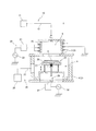
まず、本発明の一実施形態に係るプラズマ加工方法の実施に用いるプラズマ加工装置1について説明する。図1に示すように、本例のプラズマ加工装置1は、内部空間の上方にプラズマ生成空間5が設定され、このプラズマ生成空間5よりも下方に処理空間6が設定される円筒状の処理チャンバ2と、前記プラズマ生成空間5に処理ガスを供給する処理ガス供給機構10と、前記プラズマ生成空間5内に誘導電界を発生させるための環状のコイル15と、このコイル15に高周波電力を供給するコイル電力供給機構20と、前記処理空間6内に配設され、基板Kを載置するための基台25と、この基台25に高周波電力を供給する基台電力供給機構30と、処理チャンバ2内の気体を排気する排気装置35とを備えている。
[Plasma processing equipment]
First, the
前記処理チャンバ2は、アルミ合金からなる上チャンバ3及び下チャンバ4から構成されている。また、上チャンバ3及び下チャンバ4は、相互に連通した内部空間をそれぞれ有しており、上チャンバ3の内部空間がプラズマ生成空間5であり、下チャンバ4の内部空間が処理空間6である。尚、上チャンバ3は下チャンバ4よりも小さく形成される。
The
前記処理ガス供給機構10は、処理ガスが貯留された処理ガス供給源11と、一方端が処理ガス供給源11に接続し、他方端が前記上チャンバ3の天板に形成された吐出口に接続した供給管12とからなる。この処理ガス供給機構10によれば、処理ガス供給源11から供給管12を介し、前記吐出口から垂直下方に向けて処理ガスが吐出され、上チャンバ3の内部空間に処理ガスが供給される。尚、前記処理ガスは、エッチングされる基板の種類によって異なるものであり、基板がシリコン基板である場合には、SF6ガスやIF5ガス、NF3ガス、F2ガスなどのエッチングガス、C4F8ガスやO2ガス、2,3,3,3−テトラフルオロプロペンガス(HFO−1234yf)などの保護膜形成ガスを例示することができる。保護膜形成ガスとしては、温室効果ガス排出削減及びエッチングレート向上の観点から、2,3,3,3−テトラフルオロプロペンガスが好ましい。また、炭化珪素基板である場合には、エッチングガスとしてSF6ガスやSiF4ガス、CF4ガス、CH3Fガス、保護膜形成ガスとしてO2ガスやSiF4ガス、SiCl4ガスなどを例示することができ、前記処理ガス供給源11は、用いられる処理ガスの数に応じて1つ以上設けられる。
The processing
前記コイル15は、前記上チャンバ3の外周に捲回されており、コイル電力供給機構20によって高周波電力が供給されるようになっている。
The
また、前記コイル電力供給機構20は、前記コイル15に接続されたマッチングユニット21や、このマッチングユニット21に接続された高周波電源22からなり、前記コイル15に高周波電力を供給する機構である。このコイル電力供給機構20によれば、コイル15に高周波電力が供給されることで、プラズマ生成空間5内に誘導電界が発生し、当該プラズマ生成空間5内に供給された処理ガスがプラズマ化され、所謂誘導結合プラズマ(ICP)が生成される。
The coil
前記基台25は、基板Kが載置される上部材26と、昇降シリンダ28が接続された下部材27とから構成され、前記下チャンバ4の内部空間(処理空間6)に配置されている。
The
前記基台電力供給機構30は、前記基台25に接続されたマッチングユニット31と、このマッチングユニット31に接続された高周波電源32とからなり、前記基台25に高周波電力を供給する機構である。この基台電力供給機構30によれば、基台25に高周波電力が供給されることで、基台25とプラズマとの間にバイアス電位が与えられる。
The base
前記排気装置35は、気体を排気する真空ポンプ36と、一端が前記真空ポンプ36に接続し、他端が下チャンバ4の側面に開口する排気口に接続した排気管37とからなる。この排気装置35によれば、真空ポンプ36によって処理チャンバ2内の気体を排気し、処理チャンバ2の内部空間が所定圧力に維持される。
The
[プラズマ加工方法]
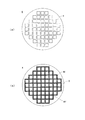
次に、以上の構成を備えたプラズマ加工装置1を用いて、基板Kをプラズマエッチングし、当該基板Kからより小さい基板K1を切り出す過程について、図2〜図4を参照して説明する。尚、本例において、基板Kは半導体素子が形成される前のシリコン基板である。また、図2は基板Kの平面図であり、図3及び図4は基板K1を切り出す過程を模式的に示した図であり、図2〜図4中の各符号は、Kが基板、K1が切り出される(切り出された)基板、Mfが表面側マスク、Sがテープ、Dが加工領域、Tがトレンチ、T1,T2がトレンチTの角部をそれぞれ示している。
[Plasma processing method]
Next, a process of plasma etching the substrate K using the
まず、切り出される基板K1の厚みを所望の厚さにするために、基板Kをプラズマ加工装置1内に搬入して基台25上に載置し、基板Kの表面全体をエッチングする(シンニング(薄化)工程)。具体的には、処理ガス供給機構10によって処理チャンバ2内にSF6ガスを所定の流量で供給し、コイル電力供給機構20及び基台電力供給機構30によってコイル15及び基台25に高周波電力を印加する。尚、処理チャンバ2内の圧力は、前記排気装置35によって所定の圧力まで減圧されている。
First, in order to obtain a desired thickness of the substrate K1 to be cut out, the substrate K is loaded into the
これにより、処理チャンバ2内に供給したSF6ガスがプラズマ化され、当該プラズマに含まれるエッチング種とシリコン原子との化学反応によって基板Kの表面全面がエッチングされる。
Thereby, SF 6 gas supplied into the
次に、基板Kを処理チャンバ2から搬出し、表面側マスク形成工程を実施する。この表面側マスク形成工程では、例えば、蒸着法(化学気相蒸着法(CVD)や物理気相蒸着法(PVD))、フォトレジストの塗布などによって、加工領域Dに対応する部分にのみ開口部Mf1が形成された所定パターンの表面側マスクMfを形成させる(図2参照)。尚、図2では、加工領域Dを網掛けで示した。また、表面側マスクMfとしては、レジストマスクや酸化膜、メタルマスク、積層膜などを例示することができる。
Next, the substrate K is unloaded from the
本例においては、切り出された基板K1の平面形状が円形となるように、上面視環状の加工領域Dを設定しているが、要求される基板K1の平面形状に応じて適宜設定すれば良い。また、加工領域Dの幅hや、加工領域D間の最小間隔pは、切り出すことのできる基板の枚数と、エッチングレートやエッチングの均一性とを考慮して、均一な基板を効率良く切り出すことができるように適宜設定すれば良く、例えば、加工領域Dの幅hは10〜200μm程度、加工領域D間の最小間隔pdは1〜2mm程度である。 In this example, the annular processing region D is set so that the planar shape of the cut out substrate K1 is circular, but may be appropriately set according to the required planar shape of the substrate K1. . In addition, the width h of the processing region D and the minimum interval p between the processing regions D can be efficiently cut out in consideration of the number of substrates that can be cut out and the etching rate and etching uniformity. For example, the width h of the processing region D is about 10 to 200 μm, and the minimum interval pd between the processing regions D is about 1 to 2 mm.
次に、表面側マスクMfを形成させた基板Kを処理チャンバ2内の基台25上に載置して、当該基板Kに対して表面側エッチング工程を実施する。尚、本例においては、基板Kの裏面に絶縁性を有するテープSを貼付するようにし(図3(a)参照)、切り出した際に基板K1が四散しないようにしている。
Next, the substrate K on which the surface-side mask Mf is formed is placed on the base 25 in the
表面側エッチング工程においては、処理ガス供給機構10によって、処理チャンバ2内にSF6ガス、C4F8ガス及びO2ガスを所定の流量で供給し、コイル電力供給機構20及び基台電力供給機構30によってコイル15及び基台25に高周波電力を印加し、また、処理チャンバ2内の圧力が所定の圧力となるように、排気装置35によって処理チャンバ2内の気体を排気する。
In the surface side etching process, SF 6 gas, C 4 F 8 gas and O 2 gas are supplied into the
これにより、処理チャンバ2内に供給したSF6ガス、C4F8ガス及びO2ガスがプラズマ化され、表面側マスクMfの開口部を通して、基板Kへの保護膜の形成及び除去が並行して行われつつ、SF6ガスのプラズマ化により生成したエッチング種(例えばフッ素ラジカル)がシリコン原子と化学反応することによって基板Kが等方的にエッチングされる。この表面側エッチング工程を所定時間実施することで、図3(b)に示すように、加工領域Dがエッチングされるとともに、表面側マスクMfの直下部もエッチングされ、基板Kにテーパ形状のトレンチTが形成される。尚、表面側エッチング工程でエッチングされたマスク直下部の形状は処理条件によって変化するため、当該表面側エッチング工程の処理条件を調整して表面外周縁部を所望の形状にすることができる。
As a result, the SF 6 gas, C 4 F 8 gas, and O 2 gas supplied into the
ついで、貫通工程を実施する。具体的に、この貫通工程では、前記表面側エッチング工程で形成されたトレンチTに保護膜を形成する処理(保護膜形成処理)と、前記トレンチTの底部から保護膜を除去するとともに、前記加工領域Dをエッチングする(エッチング処理)とを繰り返すサイクルを複数回行う。 Next, a penetration process is performed. Specifically, in this penetration step, a process of forming a protective film in the trench T formed in the surface side etching process (protective film forming process), removing the protective film from the bottom of the trench T, and performing the processing A cycle in which the region D is etched (etching process) is repeated a plurality of times.
まず、保護膜形成処理では、処理チャンバ2内にC4F8ガスを所定の流量で供給し、コイル電力供給機構20によってコイル15に高周波電力を印加し、また、処理チャンバ2内の圧力が所定の圧力となるように、排気装置35によって処理チャンバ2内の気体を排気する。これにより、前記表面側エッチング工程で形成されたトレンチTの内壁に保護膜が形成される。
First, in the protective film forming process, C 4 F 8 gas is supplied into the
ついで、エッチング処理を行う。このエッチング処理では、処理チャンバ2内にSF6ガスを所定流量で供給し、コイル電力供給機構20及び基台電力供給機構30によってコイル15及び基台25に高周波電力を供給し、また、処理チャンバ2内の圧力が所定の圧力となるように、排気装置35によって処理チャンバ2内の気体を排気する。
Next, an etching process is performed. In this etching process, SF 6 gas is supplied into the
これにより、処理チャンバ2内に供給したSF6ガスがプラズマ化され、当該SF6ガスのプラズマ化により生成したフッ素イオンが基板Kに入射することで、トレンチT底部の保護膜が除去される。また、生成したフッ素イオンが基板Kに入射する、又はSF6ガスのプラズマ化により生成したエッチング種がシリコン原子と化学反応することによって、基板Kがエッチングされる(図3(c)参照)。
Thus, SF 6 gas supplied into the
以降、加工領域Dがエッチングによって除去され、基板Kに表裏面に貫通するトレンチTが形成されるまで、保護膜形成処理及びエッチング処理を一定回数繰り返し実施する。 Thereafter, the protective film forming process and the etching process are repeated a certain number of times until the processing region D is removed by etching and the trench T penetrating the front and back surfaces is formed in the substrate K.
ここで、一般的に、基板の裏面に絶縁性テープが接着されていたり、絶縁層が形成されていたりすると、所定の処理条件を採用しない限り、この絶縁性テープや絶縁層の表面がチャージアップして、プラズマ中に含まれるイオンの進行方向が曲げられ、当該絶縁性テープや絶縁層近傍のトレンチ側壁がエッチングされるというノッチング現象が発生する。一般的なエッチング加工においては、パルス状の基台高周波電力を印加するなどの対策を講じることによって、ノッチング現象の発生を抑えるようにしているが、本実施形態においては、基板Kの裏面に絶縁性のテープSを接着し、パルスを印加しない状態でエッチング処理を行うようにして、意図的にノッチング現象を発生させる。 Here, generally, when an insulating tape is adhered to the back surface of the substrate or an insulating layer is formed, the surface of the insulating tape or insulating layer is charged up unless a predetermined processing condition is adopted. As a result, the traveling direction of ions contained in the plasma is bent, and a notching phenomenon occurs in which the insulating tape and the trench side wall near the insulating layer are etched. In general etching processing, the occurrence of notching phenomenon is suppressed by taking measures such as applying pulse-shaped base high-frequency power, but in this embodiment, the back surface of the substrate K is insulated. A notching phenomenon is intentionally generated by bonding the adhesive tape S and performing the etching process without applying a pulse.
即ち、本実施形態においては、基板Kの裏面に絶縁性のテープSが接着されているため、このテープSの表面がチャージアップして、プラズマ中に含まれるイオンの進行方向が曲げられ、当該テープS近傍のトレンチT側壁がエッチングされる。これにより、切り出された基板K1の裏面外周縁部が丸面取りされた状態となる(図4(a)参照)。 That is, in this embodiment, since the insulating tape S is bonded to the back surface of the substrate K, the surface of the tape S is charged up, and the traveling direction of ions contained in the plasma is bent, The side wall of the trench T in the vicinity of the tape S is etched. As a result, the outer peripheral edge of the back surface of the cut out substrate K1 is rounded (see FIG. 4A).
その後、表面側マスクMfを除去し、仕上げ工程を行う(図4(b)参照)。この仕上げ工程では、処理チャンバ2内にSF6ガス、C4F8ガス及びO2ガスを所定流量で供給し、コイル電力供給機構20及び基台電力供給機構30によってコイル15及び基台25に高周波電力を供給し、また、処理チャンバ2内の圧力が所定の圧力となるように、排気装置35によって処理チャンバ2内の気体を排気する。
Thereafter, the surface-side mask Mf is removed and a finishing process is performed (see FIG. 4B). In this finishing step, SF 6 gas, C 4 F 8 gas, and O 2 gas are supplied into the
これにより、表面側エッチング工程でエッチングされた部分と、貫通工程でエッチングされた部分との間の角部T1や、基板K表面と表面側エッチング工程でエッチングされた部分との間の角部T2が等方的なエッチングによって丸められ、切り出された基板K1の表面外周縁部が丸面取りされた状態となる。尚、この仕上げ工程の処理条件を適宜調整することによって、基板K1の表面粗さを低減することもできる。 Thereby, corner T1 between the portion etched in the surface side etching step and the portion etched in the penetration step, and corner T2 between the surface of the substrate K and the portion etched in the surface side etching step. Is rounded by isotropic etching, and the outer peripheral edge of the cut surface of the substrate K1 is rounded. The surface roughness of the substrate K1 can be reduced by appropriately adjusting the processing conditions of the finishing process.
斯くして、図4(c)に示すように、基板Kから、表裏面の外周縁部が丸面取りされた基板K1が切り出される。そして、このプラズマ加工方法においては、貫通工程において、保護膜形成処理及びエッチング処理を交互に行ってトレンチTを形成するようにしているため、切り出された基板K1の外周面(トレンチTの側壁に相当)は、図5に示すように、所謂スキャロップ形状を有したものとなる。 Thus, as shown in FIG. 4C, the substrate K1 whose outer peripheral edge portions on the front and back surfaces are rounded off is cut out from the substrate K. In this plasma processing method, since the trench T is formed by alternately performing the protective film forming process and the etching process in the penetration process, the outer peripheral surface of the cut out substrate K1 (on the side wall of the trench T). As shown in FIG. 5, it has a so-called scallop shape.
尚、このプラズマ加工方法によれば、例えば、直径100〜450mm程度の半導体素子が形成されていない基板から直径12.5〜150mm程度の基板を切り出すことができる。 According to this plasma processing method, for example, a substrate having a diameter of about 12.5 to 150 mm can be cut out from a substrate on which a semiconductor element having a diameter of about 100 to 450 mm is not formed.
因みに、本願発明者らは、本実施形態のプラズマ加工方法を適用して、各工程を図6にまとめた処理条件で行ったところ、シリコン基板から当該シリコン基板よりも小さいシリコン基板を切り出すことに成功した。尚、切り出された基板の外周面に形成されたスキャロップ形状は、その高さt及びピッチps(図5参照)が、それぞれ約250〜400nm、約400〜600nmであった。 Incidentally, the inventors of the present application applied the plasma processing method of the present embodiment and performed each process under the processing conditions summarized in FIG. 6, and cut out a silicon substrate smaller than the silicon substrate from the silicon substrate. Successful. Note that the scallop shape formed on the outer peripheral surface of the cut out substrate had a height t and a pitch ps (see FIG. 5) of about 250 to 400 nm and about 400 to 600 nm, respectively.
また、基板Kの厚みが200μmの場合、表面側エッチング工程に要した時間は2分、貫通工程で要した時間は深さ方向へのエッチングに10分、ノッチング形状の形成に1分の計11分、仕上げ工程に要した時間は2分であり、これらの工程に要した時間(総エッチング時間)は15分であった。また、基板Kの厚みが600μmの場合、表面側エッチング工程に要した時間は2分、貫通工程で要した時間は深さ方向へのエッチングに30分、ノッチング形状の形成に3分の計33分、仕上げ工程に要した時間は2分であり、総エッチング時間は37分であった。尚、深さ方向へのエッチングに要した時間には、均一性を考慮したオーバーエッチングに要した時間も含まれる。 When the thickness of the substrate K is 200 μm, the time required for the surface side etching process is 2 minutes, the time required for the penetration process is 10 minutes for etching in the depth direction, and 1 minute for forming the notching shape. Minutes, the time required for the finishing process was 2 minutes, and the time required for these processes (total etching time) was 15 minutes. When the thickness of the substrate K is 600 μm, the time required for the surface side etching process is 2 minutes, the time required for the penetration process is 30 minutes for the etching in the depth direction, and 3 minutes for the formation of the notching shape 33 in total. Minutes, the time required for the finishing process was 2 minutes, and the total etching time was 37 minutes. Note that the time required for etching in the depth direction includes the time required for over-etching in consideration of uniformity.
以上のように、本実施形態に係るプラズマ加工方法によれば、等方的なエッチングを行う表面側エッチング工程と異方的なエッチングを行う貫通工程とを組み合わせるとともに、貫通工程においてノッチング現象を発生させるようにしていることで、表裏面の外周縁部が丸面取りされた基板K1を切り出すことができる。したがって、従来のように、基板を切り出す工程と切り出した基板を研磨する工程とを別々に行うことなく、表裏面外周縁部が面取りされた形状の基板を製造することができ、更に、基板を一枚一枚切り出すことなく、プラズマエッチング処理によって複数の基板を一括して切り出すことができるため、基板の製造コストを低く抑えることができる。 As described above, according to the plasma processing method according to the present embodiment, the surface side etching process for performing isotropic etching and the penetration process for performing anisotropic etching are combined, and a notching phenomenon is generated in the penetration process. By doing so, it is possible to cut out the substrate K1 in which the outer peripheral edges of the front and back surfaces are rounded. Therefore, unlike the conventional method, it is possible to manufacture a substrate having a shape in which the outer peripheral edge of the front and back surfaces are chamfered without separately performing the step of cutting out the substrate and the step of polishing the cut out substrate. Since a plurality of substrates can be cut out collectively by plasma etching without cutting out each piece, the manufacturing cost of the substrate can be kept low.
以上、本発明の一実施形態について説明したが、本発明の採り得る態様は何らこれに限定されるものではない。 As mentioned above, although one Embodiment of this invention was described, the aspect which can take this invention is not limited to this at all.
上例においては、シンニング工程を実施するようにしているが、切り出される基板K1の厚さがもとの基板Kの厚さと同じで良い場合などのように、厚みを調整する必要がない場合には、シンニング工程を省略しても良い。 In the above example, the thinning process is performed. However, when it is not necessary to adjust the thickness as in the case where the thickness of the substrate K1 to be cut out may be the same as the thickness of the original substrate K, etc. The thinning process may be omitted.
また、上例では、表面側マスクMfのパターンを加工領域Dに対応する部分にのみ開口部Mf1を有するパターンとし、加工領域D以外の部分は、基板が切り出されない部分についてもマスクで覆うようにしている。しかし、例えば、図7に示すように、エッチングによって所定の平面形状(図7では円形)の基板K1のみが残るように、切り出される基板K1に対応する部分以外を加工領域Dとして設定し、切り出される基板K1に対応する部分のみがマスクに覆われるようにしても良い。尚、図7において、網掛けを付した領域が加工領域Dである。 In the above example, the pattern of the front-side mask Mf is a pattern having an opening Mf1 only in a portion corresponding to the processing region D, and a portion other than the processing region D is also covered with a mask in a portion where the substrate is not cut out. I have to. However, for example, as shown in FIG. 7, a portion other than the portion corresponding to the substrate K1 to be cut out is set as the processing region D so that only the substrate K1 having a predetermined planar shape (circular in FIG. 7) remains by etching. Only the portion corresponding to the substrate K1 to be covered may be covered with the mask. In FIG. 7, the shaded area is the machining area D.
更に、上例では、表面側エッチング工程においてテーパ形状のトレンチを形成するようにしているが、表面側マスクの直下部がエッチングされ、切り出された基板の表面外周縁部が面取りされた状態になるのであれば、表面側エッチング工程において形成されるトレンチの形状は特に限定されるものではない。したがって、表面側エッチング工程における基板を等方的にエッチングする手法及びその処理条件は、基板の材質や目的とするトレンチの形状等に合わせて適宜選択すれば良い。 Furthermore, in the above example, a tapered trench is formed in the surface side etching step, but the portion directly under the surface side mask is etched, and the outer peripheral edge portion of the cut substrate is chamfered. If it is, the shape of the trench formed in a surface side etching process will not be specifically limited. Therefore, the method and processing conditions for isotropically etching the substrate in the surface side etching step may be appropriately selected according to the material of the substrate, the shape of the target trench, and the like.
また、上例の貫通工程においては、保護膜形成処理とエッチング処理と繰り返すことによって、基板Kを異方的にエッチングするようにしているが、貫通工程において異方的なエッチングを行う他の態様としては、保護膜の形成と基板Kのエッチングとを同時に行うようにし、基台25に印加する電圧を徐々に大きくする方法などを例示することができ、貫通工程における基板を異方的にエッチングする手法や処理条件は、基板の材質等に合わせて適宜選択し得る。 Further, in the above penetration process, the substrate K is anisotropically etched by repeating the protective film formation process and the etching process, but other modes in which the anisotropic etching is performed in the penetration process are described. For example, a method of forming the protective film and etching the substrate K at the same time and gradually increasing the voltage applied to the base 25 can be exemplified, and the substrate is anisotropically etched in the penetration process. The technique and processing conditions to be performed can be appropriately selected according to the material of the substrate.
また、上例においては、ノッチング現象を発生させるようにして、基板Kの裏面外周縁部が丸面取りされた状態になるようにしているが、基板Kの裏面外周縁部を面取りする必要がない場合もある。その場合には、意図的にノッチング現象を発生させる必要はなく、貫通工程で基板Kに表裏面に貫通するトレンチTを形成することで、基板Kの表面外周縁部が面取りされた状態の基板K1を切り出すようにしても良い。 In the above example, the notch phenomenon is generated so that the outer peripheral edge of the back surface of the substrate K is rounded, but it is not necessary to chamfer the outer peripheral edge of the back surface of the substrate K. In some cases. In that case, it is not necessary to intentionally generate the notching phenomenon, and the substrate in a state where the outer peripheral edge of the front surface of the substrate K is chamfered by forming the trench T penetrating the front and back surfaces of the substrate K in the penetration process. K1 may be cut out.
更に、上例では、仕上げ工程を実施するようにして、表裏面外周縁部が丸面取りされた状態、言い換えれば、角部のない滑らかな状態にするようにしているが、丸面取りである必要がない場合や表面側エッチング工程及び貫通工程の処理条件を調整することによって対応できる場合には、仕上げ工程を実施しなくとも良い。 Furthermore, in the above example, the finishing process is performed so that the outer and outer peripheral edges of the front and back surfaces are rounded, in other words, a smooth state with no corners, but rounded chamfering is necessary. In the case where there is no problem, or when it can be dealt with by adjusting the processing conditions of the surface side etching step and the penetration step, the finishing step may not be performed.
また、上例においては、基板Kの裏面に絶縁性のテープSを貼付するようにしているが、例えば、基板Kの裏面に絶縁層を形成するようにしても良い。 In the above example, the insulating tape S is attached to the back surface of the substrate K. However, for example, an insulating layer may be formed on the back surface of the substrate K.
更に、上例では、貫通工程で意図的にノッチング現象を発生させることにより、切り出される基板の裏面外周縁部が面取りされた状態になるようにしている。しかしながら、炭化珪素基板などの比較的エッチングし難い基板では、ノッチングが発生し難いため、切り出された基板の裏面外周縁部が面取りされていない状態になる場合がある(図8参照)。そこで、貫通工程を行った後、裏面側から基板を等方的にエッチングする裏面側エッチング工程を更に行うようにしても良い。 Furthermore, in the above example, by intentionally generating a notching phenomenon in the penetration process, the outer peripheral edge of the back surface of the substrate to be cut out is chamfered. However, in a substrate that is relatively difficult to etch, such as a silicon carbide substrate, notching is unlikely to occur, so that the outer peripheral edge of the rear surface of the cut out substrate may not be chamfered (see FIG. 8). Therefore, after performing the penetration process, a back surface side etching process for isotropically etching the substrate from the back surface side may be further performed.
具体的には、図9(a)に示すように、貫通工程実施後に表面側マスクMfを除去してから基板Kの表面にテープSを貼付して、切り出された基板K1が四散するのを防止するようにした上で、当該基板Kを表裏反転させて裏面側マスク形成工程を実施する。この裏面側マスク形成工程では、表面側マスク形成工程と同様、所定の方法によって、加工領域Dに対応する部分に開口部Mb1が形成された所定パターンの裏面側マスクMbを形成させる(図9(b)参照)。尚、この場合、表面に貼付するテープSは、絶縁性を有している必要はない。また、裏面側マスクMbとしては、レジストマスクや酸化膜、メタルマスク、積層膜などを例示することができる。 Specifically, as shown in FIG. 9A, after the surface side mask Mf is removed after the penetration process is performed, the tape S is pasted on the surface of the substrate K, and the cut out substrate K1 is scattered. Then, the substrate K is turned upside down and the back side mask forming step is performed. In this back side mask forming step, a back side mask Mb having a predetermined pattern in which an opening Mb1 is formed in a portion corresponding to the processing region D is formed by a predetermined method as in the front side mask forming step (FIG. 9 ( b)). In this case, the tape S attached to the surface does not need to have insulating properties. Further, examples of the back side mask Mb include a resist mask, an oxide film, a metal mask, and a laminated film.
ついで、裏面側マスクMbを形成させた基板Kを処理チャンバ2内の基台25上に載置し、この基板Kを等方的にエッチングする裏面側エッチング工程を実施し、前記裏面側マスクMbの開口部Mb1を通して基板Kにおける裏面側マスクMbの直下部をエッチングする。尚、この裏面側エッチング工程において、基板Kを等方的にエッチングする手法及びその処理条件は、前記表面側エッチング工程と同様に基板の材質等に合わせて適宜選択すれば良い。
Next, the substrate K on which the back-side mask Mb is formed is placed on the base 25 in the
これにより、図9(c)に示すように、切り出された基板K1の表裏面外周縁部が面取りされた状態となる。 Thereby, as shown in FIG.9 (c), the front-and-back outer peripheral part of the cut-out board | substrate K1 will be in the state chamfered.
尚、この場合も、表面側マスクMf除去後に仕上げ工程を行うようにすれば、切り出された基板K1の表裏面外周縁部が丸面取りされた状態にすることもでき、処理条件を調整することで、表面粗さの低減を図ることもできる。 In this case as well, if the finishing process is performed after removing the front-side mask Mf, the front and back outer peripheral edges of the cut out substrate K1 can be rounded, and the processing conditions can be adjusted. Thus, the surface roughness can be reduced.
以上のように、このプラズマ加工方法によっても、基板の切り出し工程と切り出した基板一枚一枚を研磨する工程とを別々に行うことなく、表裏面外周縁部が面取りされた基板を製造することができ、また、基板を一枚一枚切り出すことなく、複数の基板を一括して切り出すことができる。したがって、コストを抑えつつ、表裏面の外周縁部が面取りされた基板を製造することができる。 As described above, even with this plasma processing method, a substrate with front and back outer peripheral edges is chamfered without separately performing a substrate cutting step and a step of polishing each cut substrate. In addition, a plurality of substrates can be cut out collectively without cutting out the substrates one by one. Therefore, it is possible to manufacture a substrate whose outer peripheral edge portions on the front and back surfaces are chamfered while suppressing costs.
また、上例のプラズマ加工方法においては、表面側エッチング工程と貫通工程とを実施することで、基板K1を切り出すようにしているが、これに限られるものではなく、表面側エッチング工程を実施した後、深掘り工程、裏面側エッチング工程及び貫通工程を行うようにしても良い。これについて、図10及び図11を参照して以下説明する。 Further, in the plasma processing method of the above example, the substrate K1 is cut out by performing the surface side etching step and the penetration step. However, the present invention is not limited to this, and the surface side etching step was performed. Then, you may make it perform a deep digging process, a back surface side etching process, and a penetration process. This will be described below with reference to FIGS. 10 and 11.
上例における表面側エッチング工程を実施した後、表面側マスクMfの開口部Mf1を通して基板Kを異方的にエッチングする深掘り工程を実施し、図10(a)に示すように、基板KにトレンチTを形成する。尚、この深掘り工程において、基板Kを異方的にエッチングする手法としては、前記貫通工程と同様に、保護膜形成処理及びエッチング処理を繰り返す手法などを例示することができ、当該深掘り工程において、基板Kを異方的にエッチングする手法及びその処理条件は、適宜選択することができる。 After performing the surface side etching process in the above example, a deep digging process for anisotropically etching the substrate K through the opening Mf1 of the surface side mask Mf is performed, and as shown in FIG. A trench T is formed. In this deep digging step, as a method of anisotropically etching the substrate K, a method of repeating a protective film forming process and an etching process can be exemplified as in the case of the penetration process. The method for anisotropically etching the substrate K and its processing conditions can be selected as appropriate.
ついで、基板Kの表面からマスクMfを除去した後、基板Kの表面にテープSを貼付して、基板Kを表裏反転させて裏面側マスク形成工程を実施する(図10(b)参照)。この裏面側マスク形成工程では、表面側マスク形成工程と同様、所定の方法によって加工領域Dに対応する部分に開口部Mb1が形成された裏面側マスクMbを形成させる(図10(c)参照)。この裏面側マスクMbは、上記と同様、レジストマスクや酸化膜、メタルマスク、積層膜などである。 Next, after removing the mask Mf from the surface of the substrate K, a tape S is affixed to the surface of the substrate K, the substrate K is turned upside down, and a back side mask forming step is performed (see FIG. 10B). In this back side mask forming step, the back side mask Mb in which the opening Mb1 is formed in a portion corresponding to the processing region D is formed by a predetermined method, as in the front side mask forming step (see FIG. 10C). . The back side mask Mb is a resist mask, an oxide film, a metal mask, a laminated film, or the like as described above.
次に、裏面側マスクMbを形成させた基板Kを基台25上に載置し、この基板Kを等方的にエッチングする裏面側エッチング工程を実施して、裏面側マスクMbの開口部Mb1を通して基板Kの裏面側マスクMb直下部をエッチングする。これにより、図11(a)に示すように、基板Kの裏面側にテーパ形状のトレンチTが形成される。尚、この裏面側エッチング工程においても、基板Kを等方的にエッチングする手法及びその処理条件は、適宜選択すれば良い。
Next, the substrate K on which the back-side mask Mb is formed is placed on the
その後、貫通工程を実施する。この貫通工程では、前記深掘り工程で形成されたトレンチTの底部に貫通するまで、裏面側マスクMbの開口部Mb1を通して基板Kを異方的にエッチングする。これにより、基板Kには、表裏面に貫通し、上部及び下部がテーパ形状となったトレンチTが形成され、表裏面外周縁部が面取りされた基板K1が切り出される
(図11(b)参照)。
Thereafter, a penetration process is performed. In this penetration process, the substrate K is anisotropically etched through the opening Mb1 of the back-side mask Mb until it penetrates the bottom of the trench T formed in the deep digging process. As a result, the substrate K is formed with a trench T having a tapered shape penetrating the front and back surfaces and having upper and lower portions tapered, and the front and back outer peripheral edges are chamfered (see FIG. 11B). ).
尚、このプラズマ加工方法において、表面側マスクMfを除去した後、基板Kの表面側に仕上げ工程を実施するとともに、貫通工程実施後、裏面側マスクMbを除去してから基板Kの裏面側に仕上げ工程を実施するようにし、切り出された基板K1の表裏面外周縁部を丸面取りされた状態にするようにしても良い。また、この仕上げ工程の処理条件を調整すれば、基板Kの表面粗さを低減することも可能である。 In this plasma processing method, after removing the front side mask Mf, a finishing process is performed on the front side of the substrate K. After performing the penetration process, the back side mask Mb is removed and then the rear side of the substrate K is moved to the rear side. A finishing step may be performed so that the front and back outer peripheral edges of the cut out substrate K1 are rounded. Further, the surface roughness of the substrate K can be reduced by adjusting the processing conditions of the finishing process.
以上のように、このプラズマ加工方法においても、上記と同様の作用効果を奏する。 As described above, this plasma processing method also has the same effects as described above.
また、上例では、半導体素子形成前の基板からより小さい基板を切り出すようにしているが、本発明に係るプラズマ加工方法は、例えば、図12(a)に示すような複数の半導体素子Hが形成された基板Kから個々の半導体素子(「ダイ」ともいう)Hを切り出す場合にも用いることができる。具体的には、図12(b)に示すように、基板Kに形成された各半導体素子H間に設定された加工領域Dに対応する部分にのみ開口部Mf1を有する表面側マスクMfを形成し、上例における各工程を実施することによって、マスクMfの開口部Mf1を通して加工領域Dをエッチングして除去することで、半導体素子Hを個片化すること(「プラズマダイシング」ともいう)ができる。そして、このプラズマ加工方法を用いて個片化された半導体素子Hは、その表面側や裏面側の外周縁部が面取りされた状態になる。 In the above example, a smaller substrate is cut out from the substrate before the formation of the semiconductor element. However, in the plasma processing method according to the present invention, for example, a plurality of semiconductor elements H as shown in FIG. It can also be used when individual semiconductor elements (also referred to as “dies”) H are cut out from the formed substrate K. Specifically, as shown in FIG. 12B, a surface-side mask Mf having an opening Mf1 only in a portion corresponding to the processing region D set between the semiconductor elements H formed on the substrate K is formed. Then, by performing each step in the above example, the processing region D is removed by etching through the opening Mf1 of the mask Mf, thereby dividing the semiconductor element H into pieces (also referred to as “plasma dicing”). it can. And the semiconductor element H separated into pieces using this plasma processing method will be in the state by which the outer peripheral edge part of the surface side and the back surface side was chamfered.
以上のように、このプラズマ加工方法によれば、コストを低く抑えつつ、外周縁部が面取りされた基板たる半導体素子を製造することができる、より具体的に言えば、外周縁部が面取りされていることによって抗折強度の向上が図られた半導体素子を低コストで製造することができる。 As described above, according to this plasma processing method, it is possible to manufacture a semiconductor element that is a substrate with a chamfered outer peripheral edge while keeping costs low. More specifically, the outer peripheral edge is chamfered. Thus, a semiconductor element with improved bending strength can be manufactured at low cost.
尚、この場合において、各工程の処理条件は、表面側や裏面側の面取り幅が半導体素子Hの抗折強度の向上を図ることができる幅となるように調整すれば良く、例えば、面取り幅は1μm程度であっても良い。また、個片化される半導体素子Hは、比較的小さく、ダイシングラインが長くなる、言い換えれば、加工領域Dが広くなるため、処理に必要なガス量も多くなる。したがって、温室効果ガス排出削減の観点から、保護膜形成ガスとして、2,3,3,3−テトラフルオロプロペンガスを用いることが好ましい。 In this case, the processing conditions of each step may be adjusted so that the chamfer width on the front surface side or the back surface side is a width that can improve the bending strength of the semiconductor element H. For example, the chamfer width May be about 1 μm. In addition, the semiconductor element H to be singulated is relatively small and the dicing line becomes long, in other words, the processing region D becomes wide, so that the amount of gas necessary for processing increases. Therefore, from the viewpoint of reducing greenhouse gas emissions, it is preferable to use 2,3,3,3-tetrafluoropropene gas as the protective film forming gas.
1 プラズマ加工装置
2 処理チャンバ
5 プラズマ生成空間
6 処理空間
10 処理ガス供給機構
15 コイル
20 コイル電力供給機構
25 基台
30 基台電力供給機構
K 基板
K1 切出し基板
D 加工領域
Mf 表面側マスク
Mf1 開口部
Mb 裏面側マスク
Mb1 開口部
T トレンチ
T1,T2 角部
S テープ
DESCRIPTION OF
Claims (8)
前記基板の表面に、前記加工領域に対応した開口部を有する表面側マスクを形成する表面側マスク形成工程と、
前記基板を前記基台上に載置して、前記表面側マスクの開口部を通して前記基板を等方的にエッチングする表面側エッチング工程と、
前記表面側エッチング工程を実施した後、前記基板の裏面に貫通するまで、前記表面側マスクの開口部を通して前記基板を異方的にエッチングする貫通工程とを行うことを特徴とするプラズマ加工方法。 A plasma processing method of removing a processing region set on a substrate placed on a base in a processing chamber by plasma etching and cutting out a substrate smaller than the substrate,
A surface-side mask forming step of forming a surface-side mask having an opening corresponding to the processing region on the surface of the substrate;
A surface side etching step of placing the substrate on the base and isotropically etching the substrate through the opening of the surface side mask;
A plasma processing method comprising: performing a penetrating step of anisotropically etching the substrate through the opening of the surface-side mask after performing the surface-side etching step until penetrating the back surface of the substrate.
前記貫通工程では、ノッチングを発生させることを特徴とする請求項1又は2記載のプラズマ加工方法。 On the back surface of the substrate, an insulating layer is formed or an insulating tape is adhered,
3. The plasma processing method according to claim 1, wherein notching is generated in the penetration step.
前記貫通工程を実施した後、前記基板を表裏反転させて前記基台上に載置して、前記裏面側マスクの開口部を通して前記基板を等方的にエッチングする裏面側エッチング工程とを更に行うことを特徴とする請求項1又は2記載のプラズマ加工方法。 A back side mask forming step of forming a back side mask having an opening corresponding to the processing region on the back side of the substrate;
After carrying out the penetration step, the substrate is turned upside down and placed on the base, and a back side etching step of isotropically etching the substrate through the opening of the back side mask is further performed. The plasma processing method according to claim 1 or 2, wherein
前記基板の表面に、前記加工領域に対応した開口部を有する表面側マスクを形成する表面側マスク形成工程と、
前記基板の裏面に、前記加工領域に対応した開口部を有する裏面側マスクを形成する裏面側マスク形成工程と、
前記基板を前記基台上に載置して、前記表面側マスクの開口部を通して前記基板を等方的にエッチングする表面側エッチング工程と、
前記表面側エッチング工程を実施した後、前記表面側マスクの開口部を通して前記基板を異方的にエッチングする深掘り工程と、
前記深掘り工程実施後に、前記基板を表裏反転させて前記基台上に載置して、前記裏面側マスクの開口部を通して前記基板を等方的にエッチングする裏面側エッチング工程と、
前記裏面側エッチング工程を実施した後、前記深掘り工程で形成されたトレンチの底面に貫通するまで、前記裏面側マスクの開口部を通して前記基板を異方的にエッチングする貫通工程とを行うことを特徴とするプラズマ加工方法。 A plasma processing method of removing a processing region set on a substrate placed on a base in a processing chamber by plasma etching and cutting out a substrate smaller than the substrate,
A surface-side mask forming step of forming a surface-side mask having an opening corresponding to the processing region on the surface of the substrate;
A back side mask forming step of forming a back side mask having an opening corresponding to the processing region on the back side of the substrate;
A surface side etching step of placing the substrate on the base and isotropically etching the substrate through the opening of the surface side mask;
A deep digging step for anisotropically etching the substrate through the opening of the surface side mask after performing the surface side etching step;
After performing the deep digging step, the substrate is turned upside down and placed on the base, and a back side etching step for isotropically etching the substrate through the opening of the back side mask;
After performing the back side etching step, performing a through step of anisotropically etching the substrate through the opening of the back side mask until it penetrates the bottom surface of the trench formed in the deep digging step. A plasma processing method.
外周面にスキャロップ形状を有していることを特徴とする基板。
The outer peripheral edge of at least one of the front and back surfaces is chamfered,
A substrate characterized by having a scalloped shape on the outer peripheral surface.
Priority Applications (1)
| Application Number | Priority Date | Filing Date | Title |
|---|---|---|---|
| JP2018098774A JP2018137483A (en) | 2018-05-23 | 2018-05-23 | Plasma processing method and substrate produced using this method |
Applications Claiming Priority (1)
| Application Number | Priority Date | Filing Date | Title |
|---|---|---|---|
| JP2018098774A JP2018137483A (en) | 2018-05-23 | 2018-05-23 | Plasma processing method and substrate produced using this method |
Related Parent Applications (1)
| Application Number | Title | Priority Date | Filing Date |
|---|---|---|---|
| JP2017028763A Division JP6387131B2 (en) | 2017-02-20 | 2017-02-20 | Plasma processing method and substrate manufactured using the method |
Publications (2)
| Publication Number | Publication Date |
|---|---|
| JP2018137483A true JP2018137483A (en) | 2018-08-30 |
| JP2018137483A5 JP2018137483A5 (en) | 2019-12-12 |
Family
ID=63365751
Family Applications (1)
| Application Number | Title | Priority Date | Filing Date |
|---|---|---|---|
| JP2018098774A Pending JP2018137483A (en) | 2018-05-23 | 2018-05-23 | Plasma processing method and substrate produced using this method |
Country Status (1)
| Country | Link |
|---|---|
| JP (1) | JP2018137483A (en) |
Cited By (2)
| Publication number | Priority date | Publication date | Assignee | Title |
|---|---|---|---|---|
| WO2021005903A1 (en) * | 2019-07-11 | 2021-01-14 | 富士電機株式会社 | Silicon carbide semiconductor device and method for manufacturing silicon carbide semiconductor device |
| EP3848959A1 (en) * | 2019-12-09 | 2021-07-14 | SPTS Technologies Limited | A semiconductor wafer dicing process |
Citations (10)
| Publication number | Priority date | Publication date | Assignee | Title |
|---|---|---|---|---|
| JP2008034508A (en) * | 2006-07-27 | 2008-02-14 | Sanyo Electric Co Ltd | Semiconductor device and its manufacturing method |
| JP2009141307A (en) * | 2007-11-15 | 2009-06-25 | Fuji Electric Device Technology Co Ltd | Method of manufacturing semiconductor device |
| JP2009182059A (en) * | 2008-01-29 | 2009-08-13 | Toshiba Corp | Dry etching method |
| JP2014513868A (en) * | 2011-03-14 | 2014-06-05 | プラズマ − サーム、エルエルシー | Method and apparatus for plasma dicing semiconductor wafer |
| JP2015133460A (en) * | 2014-01-16 | 2015-07-23 | 株式会社ディスコ | Method for dividing wafer |
| JP2015133459A (en) * | 2014-01-16 | 2015-07-23 | 株式会社ディスコ | Method for dividing wafer |
| WO2015166368A1 (en) * | 2014-05-02 | 2015-11-05 | International Business Machines Corporation | Etch rate enhancement for a silicon etch process through etch chamber pretreatment |
| JP2016103658A (en) * | 2016-02-10 | 2016-06-02 | Sppテクノロジーズ株式会社 | Plasma etching device |
| JP2016131178A (en) * | 2015-01-13 | 2016-07-21 | 株式会社Sumco | Silicon wafer manufacturing method and semiconductor device manufacturing method |
| JP2016146395A (en) * | 2015-02-06 | 2016-08-12 | 株式会社テラプローブ | Method for manufacturing semiconductor device and semiconductor device |
-
2018
- 2018-05-23 JP JP2018098774A patent/JP2018137483A/en active Pending
Patent Citations (10)
| Publication number | Priority date | Publication date | Assignee | Title |
|---|---|---|---|---|
| JP2008034508A (en) * | 2006-07-27 | 2008-02-14 | Sanyo Electric Co Ltd | Semiconductor device and its manufacturing method |
| JP2009141307A (en) * | 2007-11-15 | 2009-06-25 | Fuji Electric Device Technology Co Ltd | Method of manufacturing semiconductor device |
| JP2009182059A (en) * | 2008-01-29 | 2009-08-13 | Toshiba Corp | Dry etching method |
| JP2014513868A (en) * | 2011-03-14 | 2014-06-05 | プラズマ − サーム、エルエルシー | Method and apparatus for plasma dicing semiconductor wafer |
| JP2015133460A (en) * | 2014-01-16 | 2015-07-23 | 株式会社ディスコ | Method for dividing wafer |
| JP2015133459A (en) * | 2014-01-16 | 2015-07-23 | 株式会社ディスコ | Method for dividing wafer |
| WO2015166368A1 (en) * | 2014-05-02 | 2015-11-05 | International Business Machines Corporation | Etch rate enhancement for a silicon etch process through etch chamber pretreatment |
| JP2016131178A (en) * | 2015-01-13 | 2016-07-21 | 株式会社Sumco | Silicon wafer manufacturing method and semiconductor device manufacturing method |
| JP2016146395A (en) * | 2015-02-06 | 2016-08-12 | 株式会社テラプローブ | Method for manufacturing semiconductor device and semiconductor device |
| JP2016103658A (en) * | 2016-02-10 | 2016-06-02 | Sppテクノロジーズ株式会社 | Plasma etching device |
Cited By (3)
| Publication number | Priority date | Publication date | Assignee | Title |
|---|---|---|---|---|
| WO2021005903A1 (en) * | 2019-07-11 | 2021-01-14 | 富士電機株式会社 | Silicon carbide semiconductor device and method for manufacturing silicon carbide semiconductor device |
| JP2021015880A (en) * | 2019-07-11 | 2021-02-12 | 国立研究開発法人産業技術総合研究所 | Silicon carbide semiconductor device and method of manufacturing silicon carbide semiconductor device |
| EP3848959A1 (en) * | 2019-12-09 | 2021-07-14 | SPTS Technologies Limited | A semiconductor wafer dicing process |
Similar Documents
| Publication | Publication Date | Title |
|---|---|---|
| US11488865B2 (en) | Method and apparatus for plasma dicing a semi-conductor wafer | |
| CN109804453B (en) | Method and apparatus for plasma dicing semiconductor wafers | |
| JP6387131B2 (en) | Plasma processing method and substrate manufactured using the method | |
| US9711406B2 (en) | Method and apparatus for plasma dicing a semi-conductor wafer | |
| JP6450763B2 (en) | Method and apparatus for plasma dicing a semiconductor wafer | |
| US9202721B2 (en) | Method and apparatus for plasma dicing a semi-conductor wafer | |
| JP6320505B2 (en) | Method and apparatus for plasma dicing a semiconductor wafer | |
| JP2005522874A (en) | Method for etching a substrate | |
| EP3114703B1 (en) | Method for plasma dicing a semi-conductor wafer | |
| EP3594998B1 (en) | Method for plasma dicing a semi-conductor wafer | |
| EP3413341B1 (en) | Method of plasma etching and plasma dicing | |
| TWI822715B (en) | Wide-gap semiconductor substrate, apparatus for manufacturing wide-gap semiconductor substrate, and method for manufacturing wide-gap semiconductor substrate | |
| JP2018137483A (en) | Plasma processing method and substrate produced using this method | |
| JP6279933B2 (en) | Method for manufacturing silicon carbide semiconductor element | |
| US11791137B2 (en) | Apparatus for etching substrate bevel and semiconductor fabrication method using the same | |
| JP6492288B2 (en) | Device chip manufacturing method | |
| JP2008218820A (en) | Wafer and method of manufacturing the same | |
| US20220181209A1 (en) | Element chip manufacturing method | |
| US20230020438A1 (en) | Method and apparatus for plasma dicing a semi-conductor wafer | |
| US20230343647A1 (en) | Method and apparatus for plasma dicing a semi-conductor wafer | |
| TW202338173A (en) | High-hardness substrate and fabricating method thereof achieving the effect of greatly reducing the polishing time | |
| CN115458399A (en) | Method for cracking silicon carbide wafer | |
| CN112864000A (en) | Method for removing metal deposits from substrate bevel edge region and apparatus using the same | |
| JP2018006588A (en) | Wafer processing method |
Legal Events
| Date | Code | Title | Description |
|---|---|---|---|
| A521 | Request for written amendment filed |
Free format text: JAPANESE INTERMEDIATE CODE: A523 Effective date: 20191031 |
|
| A621 | Written request for application examination |
Free format text: JAPANESE INTERMEDIATE CODE: A621 Effective date: 20191031 |
|
| A131 | Notification of reasons for refusal |
Free format text: JAPANESE INTERMEDIATE CODE: A131 Effective date: 20200901 |
|
| A977 | Report on retrieval |
Free format text: JAPANESE INTERMEDIATE CODE: A971007 Effective date: 20200831 |
|
| A521 | Request for written amendment filed |
Free format text: JAPANESE INTERMEDIATE CODE: A523 Effective date: 20201022 |
|
| A02 | Decision of refusal |
Free format text: JAPANESE INTERMEDIATE CODE: A02 Effective date: 20210216 |
|
| A521 | Request for written amendment filed |
Free format text: JAPANESE INTERMEDIATE CODE: A523 Effective date: 20210510 |
|
| C60 | Trial request (containing other claim documents, opposition documents) |
Free format text: JAPANESE INTERMEDIATE CODE: C60 Effective date: 20210510 |
|
| A911 | Transfer to examiner for re-examination before appeal (zenchi) |
Free format text: JAPANESE INTERMEDIATE CODE: A911 Effective date: 20210519 |
|
| C21 | Notice of transfer of a case for reconsideration by examiners before appeal proceedings |
Free format text: JAPANESE INTERMEDIATE CODE: C21 Effective date: 20210525 |
|
| A912 | Re-examination (zenchi) completed and case transferred to appeal board |
Free format text: JAPANESE INTERMEDIATE CODE: A912 Effective date: 20210611 |
|
| C211 | Notice of termination of reconsideration by examiners before appeal proceedings |
Free format text: JAPANESE INTERMEDIATE CODE: C211 Effective date: 20210615 |
|
| C22 | Notice of designation (change) of administrative judge |
Free format text: JAPANESE INTERMEDIATE CODE: C22 Effective date: 20210803 |
|
| C23 | Notice of termination of proceedings |
Free format text: JAPANESE INTERMEDIATE CODE: C23 Effective date: 20211019 |
|
| C03 | Trial/appeal decision taken |
Free format text: JAPANESE INTERMEDIATE CODE: C03 Effective date: 20211124 |
|
| C30A | Notification sent |
Free format text: JAPANESE INTERMEDIATE CODE: C3012 Effective date: 20211124 |