JP2018081906A5 - - Google Patents
Download PDFInfo
- Publication number
- JP2018081906A5 JP2018081906A5 JP2017159647A JP2017159647A JP2018081906A5 JP 2018081906 A5 JP2018081906 A5 JP 2018081906A5 JP 2017159647 A JP2017159647 A JP 2017159647A JP 2017159647 A JP2017159647 A JP 2017159647A JP 2018081906 A5 JP2018081906 A5 JP 2018081906A5
- Authority
- JP
- Japan
- Prior art keywords
- filler
- resin layer
- diameter
- particle diameter
- inclination
- Prior art date
- Legal status (The legal status is an assumption and is not a legal conclusion. Google has not performed a legal analysis and makes no representation as to the accuracy of the status listed.)
- Granted
Links
- 239000000945 filler Substances 0.000 description 17
- 239000011347 resin Substances 0.000 description 10
- 229920005989 resin Polymers 0.000 description 10
- 239000002245 particle Substances 0.000 description 8
- 239000006185 dispersion Substances 0.000 description 2
Images

Description
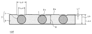
上述したフィラーの露出部分の周りの樹脂層2の傾斜2b(図1B)や、フィラーの直上の樹脂層の起伏2c(図6)の効果を得られ易くする点から傾斜2bの最大深さLeとフィラー1の粒子径Dとの比(Le/D)は、好ましくは50%未満、より好ましくは30%未満、さらに好ましくは20〜25%であり、傾斜2bや起伏2cの最大径Ldとフィラー1の粒子径Dとの比(Ld/D)は、好ましくは100%以上、より好ましくは100〜150%であり、起伏2cの最大深さLfとフィラー1の粒子径Dとの比(Lf/D)は、0より大きく、好ましくは10%未満、より好ましくは5%以下である。Resin
なお、傾斜2b又は起伏2cにおけるフィラー1の露出(直上)部分の径Lcは、フィラー1の粒子径D以下とすることができ、好ましくは粒子径Dの10〜90%である。また、フィラー1の頂部の1点で露出するようにしてもよく、粒子径Dが樹脂層2内に完全に埋まり、径Lcがゼロとなるようにしてもよい。The diameter Lc of the exposed (directly above) portion of the filler 1 in the inclination 2b or the undulation 2c can be equal to or less than the particle diameter D of the filler 1, preferably 10 to 90% of the particle diameter D. Further, it may be exposed at one point on the top of the filler 1, or the particle diameter D may be completely buried in the
1 フィラー(導電粒子)
2 樹脂層(絶縁性樹脂層)
2b 凹み(傾斜)
2c 凹み(起伏)
3 フィラー分散層(導電粒子分散層)
4 第2の樹脂層
10A、10B、10C、10D、10E、10F、10G、10H、10I フィラー含有フィルム(その一態様である異方性導電フィルム)
La 樹脂層の層厚
Lb 隣接するフィラー間の中央部における接平面とフィラーの最深部との距離
Lc 傾斜又は起伏におけるフィラーの露出(直上)部分の径
Ld フィラーの周り又は直上の樹脂層の傾斜又は起伏の最大径
Le フィラーの周りの樹脂層における傾斜の最大深さ
Lf フィラーの直上の樹脂層における起伏の最大深さ 1 Filler (conductive particles)
2 Resin layer (insulating resin layer)
2b dent (inclination)
2c dent (undulation)
3 Filler dispersion layer (conductive particle dispersion layer)
4
La resin layer thickness
Lb Distance between the tangent plane at the center between adjacent fillers and the deepest part of the filler
Diameter of exposed (directly above) portion of filler on Lc slope or undulation
Maximum diameter of inclination or undulation of the resin layer around or directly above the Ld filler
Maximum depth of inclination in the resin layer around the Le filler
Maximum depth of undulations in the resin layer directly above the Lf filler
Priority Applications (9)
| Application Number | Priority Date | Filing Date | Title |
|---|---|---|---|
| KR1020197010975A KR102359094B1 (en) | 2016-11-04 | 2017-10-27 | Filler-containing film |
| CN201780064897.6A CN109996837A (en) | 2016-11-04 | 2017-10-27 | Film containing filler |
| PCT/JP2017/038851 WO2018084075A1 (en) | 2016-11-04 | 2017-10-27 | Filler-containing film |
| US16/344,489 US11001686B2 (en) | 2016-11-04 | 2017-10-27 | Filler-containing film |
| KR1020227003492A KR102513747B1 (en) | 2016-11-04 | 2017-10-27 | Filler-containing film |
| TW111136245A TWI836624B (en) | 2016-11-04 | 2017-10-31 | Film containing filler |
| TW106137522A TWI781119B (en) | 2016-11-04 | 2017-10-31 | Film containing filler |
| US17/315,788 US20210261743A1 (en) | 2014-08-22 | 2021-05-10 | Filler-containing film |
| JP2022056054A JP7307377B2 (en) | 2016-11-04 | 2022-03-30 | Filler containing film |
Applications Claiming Priority (2)
| Application Number | Priority Date | Filing Date | Title |
|---|---|---|---|
| JP2016216233 | 2016-11-04 | ||
| JP2016216233 | 2016-11-04 |
Related Child Applications (1)
| Application Number | Title | Priority Date | Filing Date |
|---|---|---|---|
| JP2022056054A Division JP7307377B2 (en) | 2016-11-04 | 2022-03-30 | Filler containing film |
Publications (3)
| Publication Number | Publication Date |
|---|---|
| JP2018081906A JP2018081906A (en) | 2018-05-24 |
| JP2018081906A5 true JP2018081906A5 (en) | 2020-10-15 |
| JP7052254B2 JP7052254B2 (en) | 2022-04-12 |
Family
ID=62198264
Family Applications (2)
| Application Number | Title | Priority Date | Filing Date |
|---|---|---|---|
| JP2017159647A Active JP7052254B2 (en) | 2014-08-22 | 2017-08-22 | Filler-containing film |
| JP2022056054A Active JP7307377B2 (en) | 2016-11-04 | 2022-03-30 | Filler containing film |
Family Applications After (1)
| Application Number | Title | Priority Date | Filing Date |
|---|---|---|---|
| JP2022056054A Active JP7307377B2 (en) | 2016-11-04 | 2022-03-30 | Filler containing film |
Country Status (6)
| Country | Link |
|---|---|
| US (2) | US11001686B2 (en) |
| JP (2) | JP7052254B2 (en) |
| KR (2) | KR102359094B1 (en) |
| CN (1) | CN109996837A (en) |
| TW (1) | TWI781119B (en) |
| WO (1) | WO2018084075A1 (en) |
Families Citing this family (11)
| Publication number | Priority date | Publication date | Assignee | Title |
|---|---|---|---|---|
| JP6944533B2 (en) * | 2017-10-12 | 2021-10-06 | 富士フイルム株式会社 | Anisotropic conductive film and laminate |
| CN112292430A (en) * | 2018-06-06 | 2021-01-29 | 迪睿合株式会社 | Filled membranes |
| WO2019235560A1 (en) * | 2018-06-06 | 2019-12-12 | デクセリアルズ株式会社 | Filler-containing film |
| JP7452418B2 (en) * | 2018-06-26 | 2024-03-19 | 株式会社レゾナック | Anisotropic conductive film and method for producing the same, and method for producing a connected structure |
| US11240918B2 (en) * | 2018-08-28 | 2022-02-01 | Research And Business Foundation Sungkyunkwan University | Method for flip-chip bonding using anisotropic adhesive polymer |
| JP7321863B2 (en) | 2019-09-27 | 2023-08-07 | 株式会社フコク | Anisotropic pressure-sensitive conductive film |
| JP7261713B2 (en) * | 2019-09-27 | 2023-04-20 | パナソニックホールディングス株式会社 | coin cell battery |
| KR20210114596A (en) | 2020-03-10 | 2021-09-24 | 삼성디스플레이 주식회사 | Display device |
| KR20210122359A (en) | 2020-03-30 | 2021-10-12 | 삼성디스플레이 주식회사 | Display device and manufacturing method for the same |
| KR20240032918A (en) | 2021-09-22 | 2024-03-12 | 데쿠세리아루즈 가부시키가이샤 | Manufacturing method of connection structure |
| WO2023189416A1 (en) * | 2022-03-31 | 2023-10-05 | デクセリアルズ株式会社 | Electroconductive film, connection structure and manufacturing method for same |
Family Cites Families (26)
| Publication number | Priority date | Publication date | Assignee | Title |
|---|---|---|---|---|
| JP2006015680A (en) | 2004-07-05 | 2006-01-19 | Oike Ind Co Ltd | Lusterless film |
| JP2006233202A (en) * | 2005-01-31 | 2006-09-07 | Asahi Kasei Electronics Co Ltd | Anisotropically electroconductive adhesive film for circuit connection |
| US8802214B2 (en) * | 2005-06-13 | 2014-08-12 | Trillion Science, Inc. | Non-random array anisotropic conductive film (ACF) and manufacturing processes |
| JP4887700B2 (en) | 2005-09-09 | 2012-02-29 | 住友ベークライト株式会社 | Anisotropic conductive film and electronic / electrical equipment |
| JP2009074020A (en) * | 2007-03-06 | 2009-04-09 | Tokai Rubber Ind Ltd | Anisotropic conductive film |
| JP5181618B2 (en) * | 2007-10-24 | 2013-04-10 | 宇部興産株式会社 | Metal foil laminated polyimide resin substrate |
| JP2010033793A (en) * | 2008-07-28 | 2010-02-12 | Tokai Rubber Ind Ltd | Method for manufacturing particle transfer film |
| JP2010067360A (en) * | 2008-09-08 | 2010-03-25 | Tokai Rubber Ind Ltd | Anisotropic conductive film and its use method |
| KR101156177B1 (en) * | 2010-06-16 | 2012-06-18 | 한국생산기술연구원 | Anisotropic Conductive Film Having Containing Groove of Conductive Material, Joining Method of Flip Chip Using Epoxy Resin Having Containing Groove of Conductive Material and Flip Chip Package Using the Same |
| JP5297418B2 (en) * | 2010-06-21 | 2013-09-25 | デクセリアルズ株式会社 | Anisotropic conductive material and method for manufacturing the same, and mounting body and method for manufacturing the same |
| US9475963B2 (en) * | 2011-09-15 | 2016-10-25 | Trillion Science, Inc. | Fixed array ACFs with multi-tier partially embedded particle morphology and their manufacturing processes |
| US20140141195A1 (en) * | 2012-11-16 | 2014-05-22 | Rong-Chang Liang | FIXED ARRAY ACFs WITH MULTI-TIER PARTIALLY EMBEDDED PARTICLE MORPHOLOGY AND THEIR MANUFACTURING PROCESSES |
| JP2013103368A (en) | 2011-11-11 | 2013-05-30 | Sekisui Chem Co Ltd | Multi-layer film |
| US10272598B2 (en) * | 2012-08-24 | 2019-04-30 | Dexerials Corporation | Method of producing anisotropic conductive film and anisotropic conductive film |
| WO2014030744A1 (en) | 2012-08-24 | 2014-02-27 | デクセリアルズ株式会社 | Anisotropic conductive film and manufacturing method therefor |
| JP6221285B2 (en) | 2013-03-21 | 2017-11-01 | 日立化成株式会社 | Circuit member connection method |
| KR20140139902A (en) * | 2013-05-28 | 2014-12-08 | 삼성디스플레이 주식회사 | Anisotropic conductive film laminate, display device including the same and method for display device |
| JP6119718B2 (en) | 2013-11-19 | 2017-04-26 | デクセリアルズ株式会社 | Anisotropic conductive film and connection structure |
| CN110499119B (en) * | 2013-11-19 | 2023-07-18 | 迪睿合株式会社 | Anisotropic conductive film and connection structure |
| JP6264897B2 (en) | 2014-01-23 | 2018-01-24 | トヨタ自動車株式会社 | High dielectric constant film and film capacitor |
| JP2015167106A (en) | 2014-03-04 | 2015-09-24 | 日立化成株式会社 | Anisotropic conductive film, and connection structure |
| JP6331776B2 (en) * | 2014-06-30 | 2018-05-30 | デクセリアルズ株式会社 | Anisotropic conductive film and connection structure |
| WO2016068168A1 (en) | 2014-10-28 | 2016-05-06 | デクセリアルズ株式会社 | Anisotropic conductive film, manufacturing method for same, and connection structure |
| WO2016068083A1 (en) | 2014-10-31 | 2016-05-06 | デクセリアルズ株式会社 | Anisotropic conductive film |
| KR102542797B1 (en) * | 2015-01-13 | 2023-06-14 | 데쿠세리아루즈 가부시키가이샤 | Anisotropic conductive film |
| JP6187665B1 (en) * | 2016-10-18 | 2017-08-30 | デクセリアルズ株式会社 | Anisotropic conductive film |
-
2017
- 2017-08-22 JP JP2017159647A patent/JP7052254B2/en active Active
- 2017-10-27 CN CN201780064897.6A patent/CN109996837A/en active Pending
- 2017-10-27 KR KR1020197010975A patent/KR102359094B1/en active IP Right Grant
- 2017-10-27 US US16/344,489 patent/US11001686B2/en active Active
- 2017-10-27 KR KR1020227003492A patent/KR102513747B1/en active IP Right Grant
- 2017-10-27 WO PCT/JP2017/038851 patent/WO2018084075A1/en active Application Filing
- 2017-10-31 TW TW106137522A patent/TWI781119B/en active
-
2021
- 2021-05-10 US US17/315,788 patent/US20210261743A1/en not_active Abandoned
-
2022
- 2022-03-30 JP JP2022056054A patent/JP7307377B2/en active Active
Similar Documents
| Publication | Publication Date | Title |
|---|---|---|
| JP2018081906A5 (en) | ||
| JP2016131152A5 (en) | ||
| CN104779832B (en) | A kind of high performance friction generator and preparation method thereof | |
| PH12017501262A1 (en) | Anisotropic conductive film | |
| JP2013156655A5 (en) | ||
| TWD181960S (en) | Electrical connector | |
| JP2016103476A5 (en) | ||
| JP2014526149A5 (en) | ||
| JP2019054071A5 (en) | ||
| JP2013542596A5 (en) | ||
| JP2017027935A5 (en) | Power storage device | |
| JP2018138966A5 (en) | ||
| JP2013118180A5 (en) | ||
| JP2017022017A5 (en) | ||
| JP2018006181A5 (en) | ||
| JP2020132792A5 (en) | ||
| US20140209378A1 (en) | Cable fixing assembly | |
| JP2013136844A5 (en) | ||
| CN204190918U (en) | A kind of combination audio | |
| JP2013151755A5 (en) | ||
| JP2015211180A5 (en) | ||
| JP2006199833A5 (en) | ||
| JP2015014546A5 (en) | ||
| TWM462459U (en) | Device for preventing plug from falling off | |
| JP2015130426A5 (en) | Connection method |