JP2018073913A - Magnetic sensor and production method thereof - Google Patents
Magnetic sensor and production method thereof Download PDFInfo
- Publication number
- JP2018073913A JP2018073913A JP2016209854A JP2016209854A JP2018073913A JP 2018073913 A JP2018073913 A JP 2018073913A JP 2016209854 A JP2016209854 A JP 2016209854A JP 2016209854 A JP2016209854 A JP 2016209854A JP 2018073913 A JP2018073913 A JP 2018073913A
- Authority
- JP
- Japan
- Prior art keywords
- layer
- magnetoresistive element
- ferromagnetic layer
- ferromagnetic
- magnetization
- Prior art date
- Legal status (The legal status is an assumption and is not a legal conclusion. Google has not performed a legal analysis and makes no representation as to the accuracy of the status listed.)
- Pending
Links
Images


Classifications
-
- G—PHYSICS
- G01—MEASURING; TESTING
- G01R—MEASURING ELECTRIC VARIABLES; MEASURING MAGNETIC VARIABLES
- G01R33/00—Arrangements or instruments for measuring magnetic variables
- G01R33/02—Measuring direction or magnitude of magnetic fields or magnetic flux
- G01R33/06—Measuring direction or magnitude of magnetic fields or magnetic flux using galvano-magnetic devices
- G01R33/09—Magnetoresistive devices
- G01R33/093—Magnetoresistive devices using multilayer structures, e.g. giant magnetoresistance sensors
-
- G—PHYSICS
- G01—MEASURING; TESTING
- G01R—MEASURING ELECTRIC VARIABLES; MEASURING MAGNETIC VARIABLES
- G01R33/00—Arrangements or instruments for measuring magnetic variables
- G01R33/02—Measuring direction or magnitude of magnetic fields or magnetic flux
- G01R33/06—Measuring direction or magnitude of magnetic fields or magnetic flux using galvano-magnetic devices
- G01R33/09—Magnetoresistive devices
- G01R33/098—Magnetoresistive devices comprising tunnel junctions, e.g. tunnel magnetoresistance sensors
-
- H—ELECTRICITY
- H01—ELECTRIC ELEMENTS
- H01F—MAGNETS; INDUCTANCES; TRANSFORMERS; SELECTION OF MATERIALS FOR THEIR MAGNETIC PROPERTIES
- H01F10/00—Thin magnetic films, e.g. of one-domain structure
- H01F10/32—Spin-exchange-coupled multilayers, e.g. nanostructured superlattices
- H01F10/324—Exchange coupling of magnetic film pairs via a very thin non-magnetic spacer, e.g. by exchange with conduction electrons of the spacer
- H01F10/325—Exchange coupling of magnetic film pairs via a very thin non-magnetic spacer, e.g. by exchange with conduction electrons of the spacer the spacer being noble metal
-
- H—ELECTRICITY
- H01—ELECTRIC ELEMENTS
- H01F—MAGNETS; INDUCTANCES; TRANSFORMERS; SELECTION OF MATERIALS FOR THEIR MAGNETIC PROPERTIES
- H01F10/00—Thin magnetic films, e.g. of one-domain structure
- H01F10/32—Spin-exchange-coupled multilayers, e.g. nanostructured superlattices
- H01F10/324—Exchange coupling of magnetic film pairs via a very thin non-magnetic spacer, e.g. by exchange with conduction electrons of the spacer
- H01F10/3254—Exchange coupling of magnetic film pairs via a very thin non-magnetic spacer, e.g. by exchange with conduction electrons of the spacer the spacer being semiconducting or insulating, e.g. for spin tunnel junction [STJ]
-
- H—ELECTRICITY
- H01—ELECTRIC ELEMENTS
- H01F—MAGNETS; INDUCTANCES; TRANSFORMERS; SELECTION OF MATERIALS FOR THEIR MAGNETIC PROPERTIES
- H01F10/00—Thin magnetic films, e.g. of one-domain structure
- H01F10/32—Spin-exchange-coupled multilayers, e.g. nanostructured superlattices
- H01F10/324—Exchange coupling of magnetic film pairs via a very thin non-magnetic spacer, e.g. by exchange with conduction electrons of the spacer
- H01F10/3286—Spin-exchange coupled multilayers having at least one layer with perpendicular magnetic anisotropy
-
- H—ELECTRICITY
- H01—ELECTRIC ELEMENTS
- H01F—MAGNETS; INDUCTANCES; TRANSFORMERS; SELECTION OF MATERIALS FOR THEIR MAGNETIC PROPERTIES
- H01F41/00—Apparatus or processes specially adapted for manufacturing or assembling magnets, inductances or transformers; Apparatus or processes specially adapted for manufacturing materials characterised by their magnetic properties
- H01F41/14—Apparatus or processes specially adapted for manufacturing or assembling magnets, inductances or transformers; Apparatus or processes specially adapted for manufacturing materials characterised by their magnetic properties for applying magnetic films to substrates
- H01F41/30—Apparatus or processes specially adapted for manufacturing or assembling magnets, inductances or transformers; Apparatus or processes specially adapted for manufacturing materials characterised by their magnetic properties for applying magnetic films to substrates for applying nanostructures, e.g. by molecular beam epitaxy [MBE]
- H01F41/302—Apparatus or processes specially adapted for manufacturing or assembling magnets, inductances or transformers; Apparatus or processes specially adapted for manufacturing materials characterised by their magnetic properties for applying magnetic films to substrates for applying nanostructures, e.g. by molecular beam epitaxy [MBE] for applying spin-exchange-coupled multilayers, e.g. nanostructured superlattices
-
- H—ELECTRICITY
- H01—ELECTRIC ELEMENTS
- H01F—MAGNETS; INDUCTANCES; TRANSFORMERS; SELECTION OF MATERIALS FOR THEIR MAGNETIC PROPERTIES
- H01F41/00—Apparatus or processes specially adapted for manufacturing or assembling magnets, inductances or transformers; Apparatus or processes specially adapted for manufacturing materials characterised by their magnetic properties
- H01F41/32—Apparatus or processes specially adapted for manufacturing or assembling magnets, inductances or transformers; Apparatus or processes specially adapted for manufacturing materials characterised by their magnetic properties for applying conductive, insulating or magnetic material on a magnetic film, specially adapted for a thin magnetic film
- H01F41/34—Apparatus or processes specially adapted for manufacturing or assembling magnets, inductances or transformers; Apparatus or processes specially adapted for manufacturing materials characterised by their magnetic properties for applying conductive, insulating or magnetic material on a magnetic film, specially adapted for a thin magnetic film in patterns, e.g. by lithography
-
- H—ELECTRICITY
- H10—SEMICONDUCTOR DEVICES; ELECTRIC SOLID-STATE DEVICES NOT OTHERWISE PROVIDED FOR
- H10B—ELECTRONIC MEMORY DEVICES
- H10B61/00—Magnetic memory devices, e.g. magnetoresistive RAM [MRAM] devices
-
- H—ELECTRICITY
- H10—SEMICONDUCTOR DEVICES; ELECTRIC SOLID-STATE DEVICES NOT OTHERWISE PROVIDED FOR
- H10N—ELECTRIC SOLID-STATE DEVICES NOT OTHERWISE PROVIDED FOR
- H10N50/00—Galvanomagnetic devices
- H10N50/01—Manufacture or treatment
-
- H—ELECTRICITY
- H10—SEMICONDUCTOR DEVICES; ELECTRIC SOLID-STATE DEVICES NOT OTHERWISE PROVIDED FOR
- H10N—ELECTRIC SOLID-STATE DEVICES NOT OTHERWISE PROVIDED FOR
- H10N50/00—Galvanomagnetic devices
- H10N50/10—Magnetoresistive devices
-
- H—ELECTRICITY
- H10—SEMICONDUCTOR DEVICES; ELECTRIC SOLID-STATE DEVICES NOT OTHERWISE PROVIDED FOR
- H10N—ELECTRIC SOLID-STATE DEVICES NOT OTHERWISE PROVIDED FOR
- H10N50/00—Galvanomagnetic devices
- H10N50/80—Constructional details
-
- H—ELECTRICITY
- H10—SEMICONDUCTOR DEVICES; ELECTRIC SOLID-STATE DEVICES NOT OTHERWISE PROVIDED FOR
- H10N—ELECTRIC SOLID-STATE DEVICES NOT OTHERWISE PROVIDED FOR
- H10N50/00—Galvanomagnetic devices
- H10N50/80—Constructional details
- H10N50/85—Magnetic active materials
-
- H—ELECTRICITY
- H10—SEMICONDUCTOR DEVICES; ELECTRIC SOLID-STATE DEVICES NOT OTHERWISE PROVIDED FOR
- H10N—ELECTRIC SOLID-STATE DEVICES NOT OTHERWISE PROVIDED FOR
- H10N59/00—Integrated devices, or assemblies of multiple devices, comprising at least one galvanomagnetic or Hall-effect element covered by groups H10N50/00 - H10N52/00
Abstract
Description
本発明は、磁気センサおよびその製造方法に関するものである。 The present invention relates to a magnetic sensor and a manufacturing method thereof.
近年、磁気抵抗素子を備え、磁場強度に応じて出力が変化する磁気センサが提案されている。磁気抵抗素子は、磁化方向が固定された固定層と、磁化方向が可変とされた自由層と、固定層と自由層との間に配置された非磁性体で構成される中間層とを備えており、固定層の磁化方向と自由層の磁化方向との間の角度によって抵抗値が変化するものである。 In recent years, a magnetic sensor that includes a magnetoresistive element and whose output changes in accordance with the magnetic field strength has been proposed. The magnetoresistive element includes a fixed layer whose magnetization direction is fixed, a free layer whose magnetization direction is variable, and an intermediate layer composed of a nonmagnetic material disposed between the fixed layer and the free layer. The resistance value changes depending on the angle between the magnetization direction of the fixed layer and the magnetization direction of the free layer.
このような磁気センサでは、固定層が互いに逆の向きに磁化された複数の磁気抵抗素子を組み合わせてブリッジ回路を形成することにより、温度変化をキャンセルし、精度を向上させることができる。従って、同一チップ内に固定層が互いに逆の向きに磁化された複数の磁気抵抗素子を形成する技術が求められている。 In such a magnetic sensor, a change in temperature can be canceled and accuracy can be improved by forming a bridge circuit by combining a plurality of magnetoresistive elements whose fixed layers are magnetized in opposite directions. Therefore, there is a need for a technique for forming a plurality of magnetoresistive elements in which fixed layers are magnetized in opposite directions in the same chip.
しかしながら、通常、固定層の磁化方向は、チップ全体の磁場中熱処理によってのみ決定されるため、同一チップ内で同じとなる。したがって、固定層が互いに逆の向きに磁化された複数の磁気抵抗素子を備える磁気センサを製造するためには、例えば、別々に製造された複数の磁気抵抗素子を組み合わせて配置する必要があり、磁気センサの製造工程が複雑になる。 However, since the magnetization direction of the fixed layer is usually determined only by the heat treatment in the magnetic field of the entire chip, it is the same in the same chip. Therefore, in order to manufacture a magnetic sensor including a plurality of magnetoresistive elements whose fixed layers are magnetized in opposite directions, for example, it is necessary to arrange a plurality of separately manufactured magnetoresistive elements in combination. The manufacturing process of the magnetic sensor becomes complicated.
また、例えば特許文献1では、固定層の下に設けた配線に電流を流し、これにより発生した磁場を用いて、面内方向に磁気異方性を有する固定層を着磁し、磁気抵抗素子の磁化方向をチップ上で制御する方法が提案されている。
Also, for example, in
しかしながら、特許文献1に記載の方法では、固定層に面内方向の磁場が印加される。そのため、垂直磁気異方性を有する複数の磁気抵抗素子が同一チップ内に形成された磁気センサにおいて、複数の磁気抵抗素子を着磁し、各磁気抵抗素子が備える固定層を互いに逆の向きに磁化することはできない。
However, in the method described in
なお、ブリッジ回路を形成しない場合であっても、固定層が互いに逆の向きに磁化された複数の磁気抵抗素子を同一チップ内に形成する場合には、同様の問題が発生する。 Even when the bridge circuit is not formed, the same problem occurs when a plurality of magnetoresistive elements whose fixed layers are magnetized in opposite directions are formed in the same chip.
本発明は上記点に鑑みて、垂直磁気異方性を有する複数の磁気抵抗素子が同一チップ内に形成され、各磁気抵抗素子が備える固定層が互いに逆の向きに磁化された磁気センサにおいて、製造工程を簡略化することを目的とする。 In view of the above points, the present invention provides a magnetic sensor in which a plurality of magnetoresistive elements having perpendicular magnetic anisotropy are formed in the same chip, and the fixed layers of each magnetoresistive element are magnetized in opposite directions. The purpose is to simplify the manufacturing process.
上記目的を達成するため、請求項1に記載の発明では、基板(1)と、基板の一面(11)に形成された第1磁気抵抗素子(2a)および第2磁気抵抗素子(2b)と、を備え、第1磁気抵抗素子および第2磁気抵抗素子は、それぞれ、一面に垂直な磁化容易軸を有し、磁化方向が固定された固定層(21)と、磁化方向が可変とされた自由層(23)と、非磁性体で構成され、固定層と自由層との間に配置された中間層(22)と、を備え、固定層は、第1強磁性層(211)と、第2強磁性層(213)と、第1強磁性層と第2強磁性層との間に配置された非磁性層(212)と、を備え、第1磁気抵抗素子が備える第1強磁性層の磁化量は、第1磁気抵抗素子が備える第2強磁性層の磁化量よりも大きく、第2磁気抵抗素子が備える第1強磁性層の磁化量は、第2磁気抵抗素子が備える第2強磁性層の磁化量よりも小さい。 In order to achieve the above object, according to the first aspect of the present invention, there is provided a substrate (1), a first magnetoresistive element (2a) and a second magnetoresistive element (2b) formed on one surface (11) of the substrate. The first magnetoresistive element and the second magnetoresistive element each have an easy axis perpendicular to one surface and a fixed layer (21) in which the magnetization direction is fixed, and the magnetization direction is variable A free layer (23), and an intermediate layer (22) made of a nonmagnetic material and disposed between the fixed layer and the free layer, the fixed layer including the first ferromagnetic layer (211), A first ferromagnetic layer including a second ferromagnetic layer (213) and a nonmagnetic layer (212) disposed between the first ferromagnetic layer and the second ferromagnetic layer. The magnetization amount of the layer is larger than the magnetization amount of the second ferromagnetic layer included in the first magnetoresistive element, and the second magnetoresistive element includes Magnetization of the ferromagnetic layer is smaller than the magnetization of the second ferromagnetic layer in which the second magnetoresistive element is provided.
第1強磁性層、非磁性層、第2強磁性層が積層された反強磁性結合構造においては、第1強磁性層および第2強磁性層のうち磁化量の大きい方が、着磁時に印加される外部磁界と同じ向きに磁化される。そして、磁化量の小さい方は、反強磁性結合により、磁化量の大きい方とは逆の向きに磁化される。 In the antiferromagnetic coupling structure in which the first ferromagnetic layer, the nonmagnetic layer, and the second ferromagnetic layer are laminated, the larger one of the first ferromagnetic layer and the second ferromagnetic layer has a larger magnetization amount during magnetization. Magnetized in the same direction as the applied external magnetic field. The smaller magnetization amount is magnetized in an opposite direction to the larger magnetization amount by antiferromagnetic coupling.
そのため、上記のように2つの強磁性層の磁化量の大小関係が2つの磁気抵抗素子で逆とされた状態で、これら2つの磁気抵抗素子の固定層を同時に着磁すると、これら2つの磁気抵抗素子において、中間層と隣り合う強磁性層が逆の向きに磁化される。したがって、垂直磁気異方性を有する複数の磁気抵抗素子が同一チップ内に形成され、各磁気抵抗素子が備える固定層が互いに逆の向きに磁化された磁気センサにおいて、製造工程を簡略化することができる。 For this reason, when the fixed layers of the two magnetoresistive elements are simultaneously magnetized in the state where the magnitude relationship between the magnetization amounts of the two ferromagnetic layers is reversed by the two magnetoresistive elements as described above, In the resistance element, the ferromagnetic layer adjacent to the intermediate layer is magnetized in the opposite direction. Therefore, in a magnetic sensor in which a plurality of magnetoresistive elements having perpendicular magnetic anisotropy are formed in the same chip and the fixed layers provided in each magnetoresistive element are magnetized in opposite directions, the manufacturing process is simplified. Can do.
また、これら2つの磁気抵抗素子において、中間層と隣り合う強磁性層が逆の向きに磁化されることにより、強磁性層、中間層、自由層で構成される部分の抵抗値の増減が、2つの磁気抵抗素子で逆となる。したがって、例えば、請求項10に記載したように、2つの第1磁気抵抗素子および2つの第2磁気抵抗素子を用いてホイートストンブリッジ回路を形成することで、出力の温度変化等をキャンセルして、測定精度を向上させることができる。 Further, in these two magnetoresistive elements, when the ferromagnetic layer adjacent to the intermediate layer is magnetized in the opposite direction, the increase / decrease in the resistance value of the portion composed of the ferromagnetic layer, the intermediate layer, and the free layer is increased. The opposite is true for the two magnetoresistive elements. Therefore, for example, as described in claim 10, by forming a Wheatstone bridge circuit using the two first magnetoresistive elements and the two second magnetoresistive elements, the temperature change of the output is canceled, Measurement accuracy can be improved.
また、請求項11に記載の発明では、基板(1)の一面(11)に第1磁気抵抗素子(2a)を形成することと、一面に第2磁気抵抗素子(2b)を形成することと、を備え、第1磁気抵抗素子を形成すること、および、第2磁気抵抗素子を形成することは、それぞれ、一面に垂直な磁化容易軸を有し、第1強磁性層(211)と、第2強磁性層(213)と、第1強磁性層と第2強磁性層との間に配置された非磁性層(212)とを備え、磁化方向が固定された固定層(21)を形成することと、第1強磁性層の上面に、非磁性体で構成された中間層(22)を形成することと、中間層の上面に、磁化方向が可変とされた自由層(23)を形成することと、を含み、固定層を形成することでは、第1磁気抵抗素子が備える第1強磁性層の磁化量が、第1磁気抵抗素子が備える第2強磁性層の磁化量よりも大きくなり、かつ、第2磁気抵抗素子が備える第1強磁性層の磁化量が、第2磁気抵抗素子が備える第2強磁性層の磁化量よりも小さくなるように固定層を形成する。
In the invention described in
このように、2つの強磁性層の磁化量の大小関係が2つの磁気抵抗素子で逆になるように固定層を形成することにより、請求項1に記載の発明と同様に、垂直磁気異方性を有する複数の磁気抵抗素子が同一チップ内に形成され、各磁気抵抗素子が備える固定層が互いに逆の向きに磁化された磁気センサにおいて、製造工程を簡略化することができる。
In this way, by forming the fixed layer so that the magnitude relationship between the magnetization amounts of the two ferromagnetic layers is reversed between the two magnetoresistive elements, the perpendicular magnetic anisotropy is similar to the invention according to
なお、上記各手段の括弧内の符号は、後述する実施形態に記載の具体的手段との対応関係の一例を示すものである。 In addition, the code | symbol in the bracket | parenthesis of each said means shows an example of a corresponding relationship with the specific means as described in embodiment mentioned later.
以下、本発明の実施形態について図に基づいて説明する。なお、以下の各実施形態相互において、互いに同一もしくは均等である部分には、同一符号を付して説明を行う。 Hereinafter, embodiments of the present invention will be described with reference to the drawings. In the following embodiments, parts that are the same or equivalent to each other will be described with the same reference numerals.
(第1実施形態)
本発明の第1実施形態について説明する。図1に示すように、本実施形態の磁気センサ100は、基板1と、磁気抵抗素子2と、配線3と、パッド4とを備えている。なお、図1では、後述する保護膜7の図示を省略している。
(First embodiment)
A first embodiment of the present invention will be described. As shown in FIG. 1, the
基板1は、シリコン等で構成されており、基板1の一面11には、複数の磁気抵抗素子2が形成されている。後述するように、磁気抵抗素子2は、強磁性層211などを有する固定層21を備えており、磁気センサ100は、強磁性層211が一面11の法線方向における一方の向きに磁化された磁気抵抗素子2aと、他方の向きに磁化された磁気抵抗素子2bとを備えている。磁気抵抗素子2a、2bはそれぞれ第1磁気抵抗素子、第2磁気抵抗素子に相当する。
The
本実施形態の磁気センサ100は、磁気抵抗素子2a、2bをそれぞれ2つ備えており、パッド4を4つ備えている。そして、2つの磁気抵抗素子2aは配線3を介してパッド4に接続されている。
The
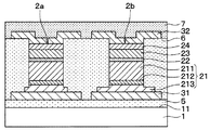
具体的には、図2に示すように、磁気センサ100は、基板1等に加えて、絶縁膜5と、側壁保護膜6と、保護膜7とを備えており、配線3は、下部配線層31と、上部配線層32とを備えている。
Specifically, as shown in FIG. 2, the
絶縁膜5は、基板1と下部配線層31とを電気的に絶縁するためのものであり、一面11に形成されている。絶縁膜5は、例えばSiO2等で構成されている。絶縁膜5の上面には下部配線層31が形成されており、2つの磁気抵抗素子2aは、下部配線層31の上面に互いに離された状態で配置されている。下部配線層31は、例えばCu、Au等で構成されている。
The insulating
側壁保護膜6は、例えばAl2O3等で構成されており、絶縁膜5、下部配線層31、および磁気抵抗素子2aを覆うように形成されている。ただし、磁気抵抗素子2aの上面は側壁保護膜6に覆われておらず、磁気抵抗素子2aの上面と側壁保護膜6の上面とに上部配線層32が形成されている。上部配線層32は、例えばCu、Au等で構成されている。
The sidewall
上部配線層32の上面にはパッド4が形成されており、一方の磁気抵抗素子2aは、上部配線層32を介して4つのパッド4のうちの1つに接続されており、他方の磁気抵抗素子2aは、上部配線層32を介して他の1つのパッド4に接続されている。なお、2つの磁気抵抗素子2bも、同様に配線3を介してパッド4に接続されている。
A
保護膜7は、側壁保護膜6と、上部配線層32と、パッド4の表面に形成されている。ただし、パッド4の上部においては保護膜7の一部が除去されて開口部71が形成されており、パッド4が露出している。
The
4つの磁気抵抗素子2は、配線3、パッド4、および、パッド4に接続された図示しないボンディングワイヤ等を介して、図示しない電源等に接続されている。
The four
磁気抵抗素子2の詳細について説明する。図2、図3に示すように、磁気抵抗素子2は、固定層21と、中間層22と、自由層23と、キャップ層24とを備えており、これらの層は、下部配線層31の上面に順に積層されている。
Details of the
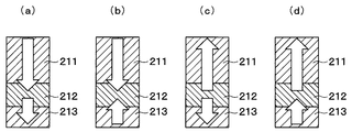
固定層21は、一面11に垂直な磁化容易軸を有しており、磁化方向が固定されている。具体的には、固定層21は、強磁性層211と、非磁性層212と、強磁性層213とを備えており、これらの層は、下部配線層31の上に、強磁性層213、非磁性層212、強磁性層211の順に積層されている。強磁性層211、213は、それぞれ、第1強磁性層、第2強磁性層に相当する。
The fixed
強磁性層211は、一面11に垂直な方向に磁化方向が固定された強磁性体膜である。図3の矢印で示すように、磁気抵抗素子2aが備える強磁性層211の磁化の向きは、磁気抵抗素子2bが備える強磁性層211の磁化の向きと逆とされている。本実施形態では、磁気抵抗素子2a、2bが備える強磁性層211は、それぞれ、強磁性層213から強磁性層211に向かう向き(図3中紙面上向き)、強磁性層211から強磁性層213に向かう向き(図3中紙面下向き)に磁化されている。
The
強磁性層211は、例えば、Co/Pt多層膜、Co/Pd多層膜で構成されている。なお、強磁性層211を、CoCr合金にPt、Ta、B、Nbなどを添加した薄膜、または、組成の異なる磁性膜の積層構造の薄膜で構成してもよい。また、強磁性層211を、Co/Pt(またはPd)多層膜とCo−Xa/(PtまたはPd)多層膜層(XaはCr、B、Ta、Mn、V)の積層磁性膜で構成してもよい。また、強磁性層211を、Co/(PtまたはPd)多層膜とCo/{(Pt−Ya)または(Pd−Ya)}多層膜層(YaはB、Ta、Ru、Re、Ir、Mn、Mg、Zr、Nb)の積層磁性膜で構成してもよい。また、強磁性層211を、CoCr合金膜とCo/(PtまたはPd)多層膜の積層磁性膜、FePt合金、CoPt合金、CoFeB薄膜などで構成してもよい。
The
非磁性層212は、Ru等の非磁性体によって形成された薄膜である。
The
強磁性層213は、一面11に垂直な方向に磁化方向が固定された強磁性体膜であり、強磁性層211と逆の向きに磁化されている。すなわち、図3の矢印で示すように、磁気抵抗素子2aが備える強磁性層213の磁化の向きは、磁気抵抗素子2bが備える強磁性層213の磁化の向きと逆とされている。本実施形態では、磁気抵抗素子2a、2bが備える強磁性層213は、それぞれ図3中紙面下向き、図3中紙面上向きに磁化されている。このように、固定層21は、互いの磁化方向が反平行となる強磁性層211と強磁性層213との間に非磁性層212を介在させた、いわゆる反強磁性結合構造を有している。強磁性層213は、例えば強磁性層211と同様の材料で構成される。
The
磁気抵抗素子2aが備える強磁性層211の磁化量は、磁気抵抗素子2aが備える強磁性層213の磁化量よりも大きくされており、磁気抵抗素子2bが備える強磁性層211の磁化量は、磁気抵抗素子2bが備える強磁性層213の磁化量よりも小さくされている。すなわち、磁気抵抗素子2aが備える強磁性層211、213の磁化量をそれぞれMA1、MA2とし、磁気抵抗素子2bが備える強磁性層211、213の磁化量をそれぞれMB1、MB2とすると、MA2<MA1、MB1<MB2とされている。
The amount of magnetization of the
磁化量は単位体積当たりの磁化量と体積との積で表される。したがって、MA1=MsA1×VA1、MA2=MsA2×VA2、MB1=MsB1×VB1、MB2=MsB2×VB2となる。なお、MsA1、MsA2は、それぞれ、磁気抵抗素子2aが備える強磁性層211、213の単位体積当たりの磁化量であり、VA1、VA2は、それぞれ、磁気抵抗素子2aが備える強磁性層211、213の体積である。また、MsB1、MsB2は、それぞれ、磁気抵抗素子2bが備える強磁性層211、213の単位体積当たりの磁化量であり、VB1、VB2は、それぞれ、磁気抵抗素子2bが備える強磁性層211、213の体積である。
The amount of magnetization is represented by the product of the amount of magnetization per unit volume and the volume. Therefore, M A1 = Ms A1 × V A1 , M A2 = Ms A2 × V A2 , M B1 = Ms B1 × V B1 , and M B2 = Ms B2 × V B2 . Ms A1 and Ms A2 are the magnetization amounts per unit volume of the
本実施形態では、磁気抵抗素子2aが備える強磁性層211、213、磁気抵抗素子2bが備える強磁性層211、213を同一の材料で構成することにより、MsA1=MsA2=MsB1=MsB2とされている。そして、VA2<VA1、VB1<VB2とすることにより、MA2<MA1、MB1<MB2とされている。
In the present embodiment, the
また、本実施形態では、強磁性層211、213が円柱状とされている。すなわち、VA1=SA1×tA1、VA2=SA2×tA2、VB1=SB1×tB1、VB2=SB2×tB2とされている。なお、SA1、SA2は、それぞれ、磁気抵抗素子2aが備える強磁性層211の上面の面積、強磁性層213の底面の面積であり、SB1、SB2は、それぞれ、磁気抵抗素子2bが備える強磁性層211の上面の面積、強磁性層213の底面の面積である。また、tA1、tA2は、それぞれ、磁気抵抗素子2aが備える強磁性層211、213の膜厚であり、tB1、tB2は、それぞれ、磁気抵抗素子2bが備える強磁性層211、213の膜厚である。
In the present embodiment, the
また、本実施形態では、rA1<rA2、rB1<rB2とされている。すなわち、SA1<SA2、SB1<SB2とされている。なお、rA1、rA2は、それぞれ、磁気抵抗素子2aが備える強磁性層211の上面の半径、強磁性層213の底面の半径であり、rB1、rB2は、それぞれ、磁気抵抗素子2bが備える強磁性層211の上面の半径、強磁性層213の底面の半径である。
In the present embodiment, r A1 <r A2 and r B1 <r B2 are set. That is, S A1 <S A2 and S B1 <S B2 . R A1 and r A2 are the radius of the upper surface of the
また、本実施形態では、rA1=rB1、tA1=tB1とされている。すなわち、SA2×tA2<SA1×tA1=SB1×tB1<SB2×tB2とされている。さらに、本実施形態では、tA2=tB2とされており、SA2<SB2、すなわち、rA2<rB2となるように、rA2、rB2が設定されている。 In this embodiment, r A1 = r B1 and t A1 = t B1 . That is, S A2 × t A2 <S A1 × t A1 = S B1 × t B1 <S B2 × t B2 . Further, in this embodiment, it is a t A2 = t B2, S A2 <S B2, i.e., so that the r A2 <r B2, r A2 , r B2 are set.
また、本実施形態では、磁気抵抗素子2aが備える非磁性層212は、上面が半径rA1の円形状とされ、底面が半径rA2の円形状とされた段付き円柱状とされている。また、磁気抵抗素子2bが備える非磁性層212は、上面が半径rB1の円形状とされ、底面が半径rB2の円形状とされた段付き円柱状とされている。
Further, in the present embodiment, the
中間層22は、固定層21の上面に形成されている。中間層22は、非磁性体で構成されており、例えば、MgO、AlO等の絶縁体によって形成され得る。この場合、磁気センサ1は、トンネル磁気抵抗(TMR:Tunneling Magneto Resistance)素子としての構成を有している。あるいは、中間層22は、例えば、Cu、Ag等の導電体によって形成され得る。この場合、磁気センサ1は、巨大磁気抵抗(GMR:Giant Magneto Resistance)素子としての構成を有している。また、中間層22を半導体によって形成してもよい。
The
自由層23は、中間層22の上面に形成されている。自由層23は、磁化方向が可変とされており、本実施形態では、一面11に平行な磁化容易軸を有する。このように、自由層23が面内磁気異方性を有する構成では、磁化困難軸方向である一面11に垂直な方向の外部磁界の検出に際して、自由層23の磁化反転が緩やかであるため、広い磁界範囲での磁界強度の検出が可能となる。
The
自由層23は、例えば、Fe、Co、Niのうちの少なくとも一つとBとを含有するアモルファス状態の合金等を用いて形成することが可能である。キャップ層24は、自由層23を保護するためのものであり、Ta、Ru等で構成されている。
The
中間層22、自由層23、キャップ層24の上面は、円形状とされており、半径が強磁性層211の上面の半径と等しくされている。すなわち、磁気抵抗素子2aが備える中間層22、自由層23、キャップ層24の上面の半径はrA1とされており、磁気抵抗素子2bが備える中間層22、自由層23、キャップ層24の上面の半径はrB1とされている。
The upper surfaces of the
磁気センサ100の製造方法について説明する。磁気センサ100は、図4〜10に示す工程を行うことによって製造される。
A method for manufacturing the
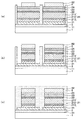
図4(a)に示す工程では、基板1の一面11に、絶縁膜5と、下部配線層31と、固定層21の強磁性層213、非磁性層212、強磁性層211と、中間層22と、自由層23と、キャップ層24とを順に成膜する。そして、キャップ層24の上面に、フォトリソグラフィにより、レジスト81を形成する。レジスト81は、図1に示す下部配線層31の上面形状に対応する形状とされている。
4A, the insulating
図4(b)に示す工程では、レジスト81をマスクとして用いたエッチングにより、下部配線層31、固定層21、中間層22、自由層23、キャップ層24の一部を除去し、下部配線層31を図1に示す形状とする。そして、エッチングにより露出した絶縁膜5と、下部配線層31、固定層21、中間層22、自由層23、キャップ層24、レジスト81とを覆うように、スパッタリング、CVD等を用いて側壁保護膜6を形成する。
In the step shown in FIG. 4B, the
図4(c)に示す工程では、レジスト81を剥離し、レジスト81の上部に形成された側壁保護膜6をリフトオフによって除去する。
In the step shown in FIG. 4C, the resist 81 is removed, and the side wall
図5(a)に示す工程では、フォトリソグラフィを行い、キャップ層24の上面にレジスト82を成膜する。レジスト82は、磁気抵抗素子2a、2bの強磁性層213に対応する形状に形成される。具体的には、レジスト82のうち磁気抵抗素子2aに対応する部分の上面は半径rA2の円形状とされ、磁気抵抗素子2bに対応する部分の上面は半径rB2の円形状とされる。
In the step shown in FIG. 5A, photolithography is performed to form a resist 82 on the upper surface of the
図5(b)に示す工程では、例えばイオンミリング等のエッチングを用いて、固定層21からキャップ層24までの各層のうち、レジスト82で覆われていない部分を除去する。これにより、磁気抵抗素子2aに対応する部分の固定層21からキャップ層24は上面の半径がrA2の円柱状となり、磁気抵抗素子2bに対応する部分の固定層21からキャップ層24は上面の半径がrB2の円柱状となる。
In the step shown in FIG. 5B, for example, etching such as ion milling is used to remove portions of the layers from the fixed
図5(c)に示す工程では、絶縁膜5、下部配線層31、固定層21、中間層22、自由層23、キャップ層24、レジスト82の表面を覆うように、スパッタリング、CVD等を用いて側壁保護膜6を形成する。
In the step shown in FIG. 5C, sputtering, CVD, or the like is used so as to cover the surfaces of the insulating
図6(a)に示す工程では、レジスト82を剥離し、側壁保護膜6のうちレジスト82の上部に形成された部分をリフトオフによって除去する。
In the step shown in FIG. 6A, the resist 82 is peeled off, and the portion of the sidewall
図6(b)に示す工程では、フォトリソグラフィを行い、キャップ層24の上面にレジスト83を成膜する。レジスト83は、磁気抵抗素子2a、2bの強磁性層211に対応する形状に形成される。具体的には、レジスト83のうち磁気抵抗素子2aに対応する部分の上面は半径rA1の円形状とされ、磁気抵抗素子2bに対応する部分の上面は半径rB1の円形状とされる。
In the step shown in FIG. 6B, photolithography is performed to form a resist 83 on the upper surface of the
図6(c)に示す工程では、エッチングを用いて、レジスト83で覆われていない部分について、少なくともキャップ層24と、自由層23と、中間層22と、強磁性層211の一部とを除去する。本実施形態では、雰囲気中に含まれる元素を分析しながらエッチングを行い、非磁性層212を構成する元素が検出されたときにエッチングを停止して、キャップ層24と、自由層23と、中間層22と、強磁性層211と、非磁性層212の一部とを除去する。
In the step shown in FIG. 6C, at least the
これにより、上面が半径rA1の円形状とされた強磁性層211、中間層22、自由層23、キャップ層24と、上面の半径がrA1、底面の半径がrA2の段付き円柱状とされた非磁性層212と、底面が半径rA2の円形状とされた強磁性層213とを備える磁気抵抗素子2aが形成される。また、上面が半径rB1の円形状とされた強磁性層211、中間層22、自由層23、キャップ層24と、上面の半径がrB1、底面の半径がrB2の段付き円柱状とされた非磁性層212と、底面が半径rB2の円形状とされた強磁性層213とを備える磁気抵抗素子2bが形成される。
Accordingly, a circular shape and
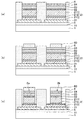
図7(a)に示す工程では、絶縁膜5、下部配線層31、磁気抵抗素子2a、2b、レジスト83の表面を覆うように、スパッタリング、CVD等を用いて側壁保護膜6を形成する。
In the step shown in FIG. 7A, the sidewall
図7(b)に示す工程では、レジスト83を剥離し、側壁保護膜6のうちレジスト83の上部に形成された部分をリフトオフによって除去する。
In the step shown in FIG. 7B, the resist 83 is removed, and a portion of the sidewall
図8(a)、図9(a)に示す工程では、フォトリソグラフィを行い、側壁保護膜6の上面にレジスト84を形成する。レジスト84には、図1に示す上部配線層32の上面形状に対応する開口部が設けられている。レジスト84を形成した後、キャップ層24、側壁保護膜6、レジスト84の表面に、上部配線層32を形成する。
In the steps shown in FIGS. 8A and 9A, photolithography is performed to form a resist 84 on the upper surface of the sidewall
図8(b)、図9(b)に示す工程では、レジスト84を剥離し、上部配線層32のうちレジスト84の上部に形成された部分をリフトオフによって除去する。
In the steps shown in FIGS. 8B and 9B, the resist 84 is peeled off, and a portion of the
図8(c)、図9(c)に示す工程では、フォトリソグラフィを用いて上部配線層32の一部を露出させる図示しないマスクを形成し、このマスクおよび上部配線層32の表面にパッド4を形成する。その後、マスクを剥離し、マスクの上部に形成されたパッド4をリフトオフによって除去する。また、上部配線層32、パッド4、側壁保護膜6の表面に保護膜7を形成し、フォトリソグラフィおよびエッチングにより、パッド4の上部に形成された保護膜7を除去し、開口部71を形成して、パッド4を露出させる。
In the steps shown in FIGS. 8C and 9C, a mask (not shown) that exposes a part of the
図10に示す工程では、磁気抵抗素子2a、2bの着磁を行う。具体的には、基板1に一面11の法線方向の磁場を印加し、磁場をある程度大きくした後、0に戻す。これにより、図10の矢印で示すように、磁気抵抗素子2aが備える強磁性層211は、強磁性層213から強磁性層211に向かう向きに磁化され、強磁性層213は、強磁性層211から強磁性層213に向かう向きに磁化される。また、磁気抵抗素子2bが備える強磁性層211は、強磁性層211から強磁性層213に向かう向きに磁化され、強磁性層213は、強磁性層213から強磁性層211に向かう向きに磁化される。
In the step shown in FIG. 10, the
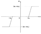
磁気抵抗素子2の着磁について、図11〜15を参照して説明する。磁化量が互いに等しい強磁性層211および強磁性層213と、これらの強磁性層の間に配置された非磁性層212とを備える固定層21に磁場を印加した場合、磁化曲線は図11に示すようになる。
Magnetization of the
すなわち、H<−Hsのとき、図12(a)に示すように強磁性層211、213は共に負の向きに磁化され、磁場Hが−Hsよりもある程度小さいときには、M=−|M1+M2|となる。なお、M1、M2はそれぞれ強磁性層211、213の磁化量であり、Mは固定層21の全体としての磁化であり、Hは固定層21に印加される磁場の強さである。また、磁化および磁場の向きについて、強磁性層213から強磁性層211に向かう向き、強磁性層211から強磁性層213に向かう向きをそれぞれ正の向き、負の向きとする。
That is, when H <−Hs, as shown in FIG. 12A, the
また、−Hs≦H<Hsのとき、図12(b)に示すように強磁性層211、213がそれぞれ負の向き、正の向きに磁化され、あるいは、図12(c)に示すように強磁性層211、213がそれぞれ正の向き、負の向きに磁化され、M=|M1−M2|=0となる。
Further, when −Hs ≦ H <Hs, the
また、Hs≦Hのとき、図12(d)に示すように強磁性層211、213が共に正の向きに磁化され、磁場HがHsよりもある程度大きいときには、M=|M1+M2|となる。
When Hs ≦ H, as shown in FIG. 12D, when the
このように、強磁性層211、213の磁化量が互いに等しい場合、H=0においてM=0となる。一方、強磁性層211、213の磁化量が互いに異なる場合、磁化曲線は図13に示すようになり、強磁性層211、213は図14、15に示すように磁化され、H=0においてM≠0となる。なお、図13において、実線は磁場Hが増加するときの磁化曲線を示し、一点鎖線は磁場Hが減少するときの磁化曲線を示す。また、図14は強磁性層211の磁化量が強磁性層213の磁化量よりも大きい場合の強磁性層211、213の磁化の向きを示し、図15は強磁性層211の磁化量が強磁性層213の磁化量よりも小さい場合の強磁性層211、213の磁化の向きを示す。
As described above, when the magnetization amounts of the
すなわち、磁場Hが増加していくと、H<−Hs2のとき、図14(a)、図15(a)に示すように強磁性層211、213は共に負の向きに磁化され、磁場Hが−Hs2よりもある程度小さいときには、M=−|M1+M2|となる。
That is, as the magnetic field H increases, when H <−Hs 2 , the
また、−Hs2≦H<Hs1のとき、図14(b)、図15(b)に示すように、強磁性層211、213のうち磁化量の大きい方が負の向きに磁化され、磁化量の小さい方が正の向きに磁化される。そして、磁場Hが−Hs2よりもある程度大きく、Hs1よりもある程度小さいときには、M=−|M1−M2|となる。
When −Hs 2 ≦ H <Hs 1 , as shown in FIGS. 14B and 15B, the
また、Hs1≦H<Hs3のとき、図14(c)、図15(c)に示すように、強磁性層211、213のうち磁化量の大きい方が正の向きに磁化され、磁化量の小さい方が負の向きに磁化される。そして、磁場HがHs1よりもある程度大きく、Hs3よりもある程度小さいときには、M=|M1−M2|となる。
Further, when Hs 1 ≦ H <Hs 3 , as shown in FIGS. 14C and 15C, the larger magnetization amount of the
また、Hs3<Hのとき、図14(d)、図15(d)に示すように強磁性層211、213は共に正の向きに磁化され、磁場HがHs3よりもある程度大きいときには、M=|M1+M2|となる。
Further, when Hs 3 <H, as shown in FIGS. 14D and 15D, the
一方、磁場Hが減少していくと、Hs2<Hのとき、図14(d)、図15(d)に示すように強磁性層211、213は共に正の向きに磁化され、磁場HがHs2よりもある程度大きいときには、M=|M1+M2|となる。
On the other hand, when the magnetic field H decreases, when Hs 2 <H, the
また、−Hs1<H≦Hs2のとき、図14(c)、図15(c)に示すように、強磁性層211、213のうち磁化量の大きい方が正の向きに磁化され、磁化量の小さい方が負の向きに磁化される。そして、磁場Hが−Hs1よりもある程度大きく、Hs2よりもある程度小さいときには、M=|M1−M2|となる。
Further, when −Hs 1 <H ≦ Hs 2 , as shown in FIGS. 14C and 15C, the one having the larger magnetization amount among the
また、−Hs3<H≦−Hs1のとき、図14(b)、図15(b)に示すように、強磁性層211、213のうち磁化量の大きい方が負の向きに磁化され、磁化量の小さい方が正の向きに磁化される。そして、磁場Hが−Hs3よりもある程度大きく、−Hs1よりもある程度小さいときには、M=−|M1−M2|となる。
Further, when −Hs 3 <H ≦ −Hs 1 , as shown in FIGS. 14B and 15B, the larger one of the
また、H≦−Hs3のとき、図14(a)、図15(a)に示すように強磁性層211、213は共に負の向きに磁化され、磁場Hが−Hs3よりもある程度小さいときには、M=−|M1+M2|となる。
When H ≦ −Hs 3 , the
このように、反強磁性結合構造を有する固定層では、非磁性層を介して結合する2つの強磁性層のうち、磁化量の大きい層が着磁時に与えられる外部磁界と同じ向きに磁化される。そして、磁化量の小さい層は、反強磁性結合により、磁化量の大きい層とは逆の向きに磁化される。 As described above, in the fixed layer having the antiferromagnetic coupling structure, of the two ferromagnetic layers coupled via the nonmagnetic layer, the layer having a large magnetization is magnetized in the same direction as the external magnetic field applied at the time of magnetization. The The layer having a small magnetization is magnetized in the opposite direction to the layer having a large magnetization by antiferromagnetic coupling.
本実施形態では、このような磁化特性を利用して、一度の着磁によって磁気抵抗素子2a、2bの強磁性層211を互いに逆の向きに磁化する。具体的には、磁場HをHs1よりも大きくした後、0に戻すことにより、磁気抵抗素子2aが備える強磁性層211、213をそれぞれ正の向き、負の向きに磁化し、磁気抵抗素子2bが備える強磁性層211、213をそれぞれ負の向き、正の向きに磁化する。
In the present embodiment, using such magnetization characteristics, the
以上説明したように、本実施形態では、強磁性層211と強磁性層213の磁化量の大小関係を磁気抵抗素子2a、2bで逆にすることにより、一度の着磁で、磁気抵抗素子2a、2bが備える強磁性層211を互いに逆の向きに磁化することができる。したがって、垂直磁気異方性を有する複数の磁気抵抗素子が同一チップ内に形成され、各磁気抵抗素子が備える固定層が互いに逆の向きに磁化された磁気センサにおいて、製造工程を簡略化することができる。また、これにより、磁気センサの製造にかかる時間を短縮し、また、製造コストを低減することができる。
As described above, in this embodiment, by reversing the magnitude relationship between the magnetization amounts of the
また、本実施形態では、磁気抵抗素子2a、2bの強磁性層211、213が同じ材料で構成され、単位体積当たりの磁化量が互いに等しくされている。そのため、強磁性層211の上面の面積、強磁性層213の底面の面積、強磁性層211、213の膜厚を制御することで、強磁性層211の磁化の向きを制御することができる。したがって、磁気センサ100の製造が容易になる。
In the present embodiment, the
なお、磁気抵抗素子2aの強磁性層211と、磁気抵抗素子2bの強磁性層211とを同時に成膜することが望ましい。また、磁気抵抗素子2aの強磁性層213と、磁気抵抗素子2bの強磁性層213についても同時に成膜することが望ましい。これらの層を同時に成膜することで、磁気抵抗素子2aと磁気抵抗素子2bとで強磁性層211、213を等しい膜厚とすることができるため、素子のばらつきを抑制し、測定誤差を低減することができる。
It is desirable to form the
また、磁気抵抗素子2aと磁気抵抗素子2bとの抵抗値の差を小さくし、また、図6(c)に示す工程におけるエッチングレートのばらつきを低減するために、SA1=SB1とすることが望ましい。
Further, in order to reduce the difference in resistance value between the
(第2実施形態)
本発明の第2実施形態について説明する。本実施形態は、第1実施形態に対して磁気抵抗素子2の数を変更したものであり、その他については第1実施形態と同様であるため、第1実施形態と異なる部分についてのみ説明する。
(Second Embodiment)
A second embodiment of the present invention will be described. In the present embodiment, the number of
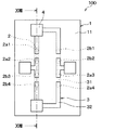
本実施形態の磁気センサ100は、磁気抵抗素子2a、2bをそれぞれ4つ備えている。4つの磁気抵抗素子2aをそれぞれ磁気抵抗素子2a1、2a2、2a3、2a4とし、4つの磁気抵抗素子2bをそれぞれ磁気抵抗素子2b1、2b2、2b3、2b4とする。
The
図16に示すように、4つの磁気抵抗素子2aおよび4つの磁気抵抗素子2bは、配線3によって電気的に接続され、図17に示すホイートストンブリッジ(フルブリッジ)回路を構成している。なお、図16では、保護膜7の図示を省略している。
As shown in FIG. 16, the four
すなわち、図示しない電源の正極と負極(グランド)との間に、2つの磁気抵抗素子2aと2つの磁気抵抗素子2bとが、磁気抵抗素子2aが正極側となるように直列に接続されている。また、この電源の正極と負極との間には、これらの磁気抵抗素子と並列となるように、他の2つの磁気抵抗素子2aと他の2つの磁気抵抗素子2bとが、磁気抵抗素子2bが正極側となるように配置されている。
That is, two
具体的には、図示しない電源の正極に、上部配線層32を介して、磁気抵抗素子2a1、2b1のキャップ層24が接続されている。磁気抵抗素子2a1、2b1の強磁性層213は、それぞれ、下部配線層31を介して磁気抵抗素子2a2、2b2の強磁性層213に接続されている。磁気抵抗素子2a2、2b2のキャップ層24は、それぞれ、上部配線層32を介して磁気抵抗素子2b3、2a3のキャップ層24に接続されている。磁気抵抗素子2b3、2a3の強磁性層213は、それぞれ、下部配線層31を介して磁気抵抗素子2b4、2a4の強磁性層213に接続されている。磁気抵抗素子2b4、2a4のキャップ層24は、それぞれ、上部配線層32を介して図示しない電源の負極に接続されている。
Specifically, the
また、図16に示すように、本実施形態の磁気センサ100は、4つのパッド4を備えている。4つのパッド4のうちの2つは、ブリッジ回路を図示しない電源に接続するために用いられ、上部配線層32のうち磁気抵抗素子2a1、2b1に接続された部分と、磁気抵抗素子2a4、2b4に接続された部分の上面に形成されている。また、他の2つは、磁気抵抗素子2a2、2b3の接続点と、磁気抵抗素子2b2、2a3の接続点との電位差を測定するために用いられ、上部配線層32のうち磁気抵抗素子2a2、2b3に接続された部分と、磁気抵抗素子2b2、2a3に接続された部分の上面に形成されている。
Further, as shown in FIG. 16, the
このような構成において、電源の正極と負極との間に所定の電圧Vccが印加されることで、図17、図18の矢印で示すように電流が流れる。 In such a configuration, when a predetermined voltage Vcc is applied between the positive electrode and the negative electrode of the power supply, a current flows as shown by arrows in FIGS.
このような磁気センサ100を製造するには、まず、図4〜7に示す工程と同様に、図16に示す形状の下部配線層31、および、各磁気抵抗素子2を形成する。その後、図19に示すように、図16に示す上部配線層32に対応する形状のレジスト84を形成し、キャップ層24、側壁保護膜6、レジスト84の表面に上部配線層32を形成する。そして、レジスト84を剥離し、レジスト84の上部に形成された上部配線層32をリフトオフによって除去し、ホイートストンブリッジ回路を形成した後、パッド4および保護膜7を形成し、図10に示す工程と同様に着磁を行う。
In order to manufacture such a
磁気抵抗素子2の抵抗値は、中間層22に接する強磁性層211の磁化方向により変化する。したがって、強磁性層211の磁化の向きを反転させることで、磁気抵抗素子2の抵抗値の出力特性が反転する。よって、磁気抵抗素子2a2と磁気抵抗素子2b3との接続点の電位V01と、磁気抵抗素子2b2と磁気抵抗素子2a3との接続点の電位V02との差に基づいて磁界検出を行うことにより、例えば温度変化などの外乱の影響が低減される。
The resistance value of the
このように温度特性を補償するためのブリッジ回路を1チップ上に構成する場合にも、強磁性層211、213の磁化量の大小関係を磁気抵抗素子2a、2bで逆にすることで、第1実施形態と同様に、磁気センサ100の製造工程を簡略化することができる。
Even when the bridge circuit for compensating the temperature characteristic is configured on one chip as described above, the
(第3実施形態)
本発明の第3実施形態について説明する。本実施形態は、第1実施形態に対してエッチングストップ層を変更したものであり、その他については第1実施形態と同様であるため、第1実施形態と異なる部分についてのみ説明する。
(Third embodiment)
A third embodiment of the present invention will be described. In the present embodiment, the etching stop layer is changed with respect to the first embodiment, and the others are the same as those in the first embodiment. Therefore, only the portions different from the first embodiment will be described.
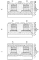
本実施形態では、図20に示すように、強磁性層211がエッチングストップ層とされている。すなわち、レジスト83を用いたエッチングにおいて、強磁性層211を構成する元素が雰囲気中に検出されたときにエッチングを停止し、キャップ層24と、自由層23と、中間層22と、強磁性層211の一部とを除去する。これにより、強磁性層211は、底面の面積が上面の面積よりも大きい段付き円柱状とされている。
In the present embodiment, as shown in FIG. 20, the
一般に、反強磁性結合構造においては、非磁性層よりも、非磁性層の両側に配置された強磁性層の膜厚が大きくされている。したがって、強磁性層211をエッチングストップ層とすることで、エッチング深さの制御が容易になり、磁気センサ100の製造が容易になる。
In general, in the antiferromagnetic coupling structure, the thickness of the ferromagnetic layer disposed on both sides of the nonmagnetic layer is larger than that of the nonmagnetic layer. Therefore, by using the
(第4実施形態)
本発明の第4実施形態について説明する。本実施形態は、第1実施形態に対してエッチングストップ層を変更したものであり、その他については第1実施形態と同様であるため、第1実施形態と異なる部分についてのみ説明する。
(Fourth embodiment)
A fourth embodiment of the present invention will be described. In the present embodiment, the etching stop layer is changed with respect to the first embodiment, and the others are the same as those in the first embodiment. Therefore, only the portions different from the first embodiment will be described.
本実施形態では、図21に示すように、強磁性層213がエッチングストップ層とされている。すなわち、レジスト83を用いたエッチングにおいて、強磁性層213を構成する元素が雰囲気中に検出されたときにエッチングを停止し、キャップ層24と、自由層23と、中間層22と、強磁性層211と、非磁性層212と、強磁性層213の一部とを除去する。これにより、強磁性層213は、底面の面積が上面の面積よりも大きい段付き円柱状とされている。
In the present embodiment, as shown in FIG. 21, the
強磁性層213をエッチングストップ層とした本実施形態においても、第3実施形態と同様に、エッチング深さの制御が容易になり、磁気センサ100の製造が容易になる。
In the present embodiment in which the
(他の実施形態)
なお、本発明は上記した実施形態に限定されるものではなく、特許請求の範囲に記載した範囲内において適宜変更が可能である。
(Other embodiments)
In addition, this invention is not limited to above-described embodiment, In the range described in the claim, it can change suitably.
例えば、MA2<MA1、MB1<MB2であれば、強磁性層211、213を上記第1〜4実施形態とは異なる構成としてもよい。例えば、強磁性層211と強磁性層213とが互いに異なる材料で構成され、MsA1≠MsA2またはMsB1≠MsB2とされていてもよい。また、MsA2<MsA1かつVA1=VA2とされていてもよく、MsB1<MsB2かつVB1=VB2とされていてもよい。また、SA1≠SB1とされていてもよい。また、tA1≠tB1、あるいは、tA2≠tB2とされていてもよい。また、SA1=SA2、あるいは、SB1=SB2とされていてもよい。
For example, if M A2 <M A1 and M B1 <M B2 , the
また、一面11に垂直な方向の外部磁界の検出に際して、広い磁界範囲で磁界強度を検出するためには、自由層23が一面11に平行な磁化容易軸を有することが望ましいが、自由層23が一面11に平行な磁化容易軸を有していなくてもよい。例えば、自由層23が一面11に垂直な磁化容易軸を有していてもよい。
In order to detect the magnetic field strength in a wide magnetic field range when detecting the external magnetic field in the direction perpendicular to the
また、磁気センサ100が磁気抵抗素子2aを1つのみ備えていてもよいし、磁気抵抗素子2bを1つのみ備えていてもよい。また、磁気抵抗素子2を構成する各層の上面が円形状とされていなくてもよい。
Further, the
また、固定層21の着磁の際、磁場Hを−Hs1よりも小さくした後、0に戻すことにより、磁気抵抗素子2aが備える強磁性層211を負の向きに磁化し、磁気抵抗素子2bが備える強磁性層211を正の向きに磁化してもよい。また、上記第2実施形態において、2つの磁気抵抗素子2aおよび2つの磁気抵抗素子2bによってホイートストンブリッジ回路を構成してもよい。また、基板1にハーフブリッジ回路を構成する磁気抵抗素子2a、2bのみが形成されていてもよい。
Further, when the pinned
また、固定層21の磁化容易軸は一面11に完全に垂直である必要はなく、一面11に略垂直であってもよい。
Further, the easy axis of magnetization of the fixed
1 基板
2a 磁気抵抗素子
2b 磁気抵抗素子
21 固定層
211 強磁性層
212 非磁性層
213 強磁性層
22 中間層
23 自由層
DESCRIPTION OF
Claims (20)
前記基板の一面(11)に形成された第1磁気抵抗素子(2a)および第2磁気抵抗素子(2b)と、を備え、
前記第1磁気抵抗素子および前記第2磁気抵抗素子は、それぞれ、
前記一面に垂直な磁化容易軸を有し、磁化方向が固定された固定層(21)と、
磁化方向が可変とされた自由層(23)と、
非磁性体で構成され、前記固定層と前記自由層との間に配置された中間層(22)と、を備え、
前記固定層は、第1強磁性層(211)と、第2強磁性層(213)と、前記第1強磁性層と前記第2強磁性層との間に配置された非磁性層(212)と、を備え、
前記第1磁気抵抗素子が備える前記第1強磁性層の磁化量は、前記第1磁気抵抗素子が備える前記第2強磁性層の磁化量よりも大きく、
前記第2磁気抵抗素子が備える前記第1強磁性層の磁化量は、前記第2磁気抵抗素子が備える前記第2強磁性層の磁化量よりも小さい磁気センサ。 A substrate (1);
A first magnetoresistive element (2a) and a second magnetoresistive element (2b) formed on one surface (11) of the substrate,
The first magnetoresistive element and the second magnetoresistive element are respectively
A fixed layer (21) having an easy axis perpendicular to the one surface and having a fixed magnetization direction;
A free layer (23) in which the magnetization direction is variable;
An intermediate layer (22) made of a non-magnetic material and disposed between the fixed layer and the free layer;
The fixed layer includes a first ferromagnetic layer (211), a second ferromagnetic layer (213), and a nonmagnetic layer (212) disposed between the first ferromagnetic layer and the second ferromagnetic layer. ) And
The magnetization amount of the first ferromagnetic layer included in the first magnetoresistive element is larger than the magnetization amount of the second ferromagnetic layer included in the first magnetoresistive element,
A magnetic sensor in which a magnetization amount of the first ferromagnetic layer included in the second magnetoresistive element is smaller than a magnetization amount of the second ferromagnetic layer included in the second magnetoresistive element.
前記第1磁気抵抗素子が備える前記第1強磁性層の体積は、前記第1磁気抵抗素子が備える前記第2強磁性層の体積よりも大きく、
前記第2磁気抵抗素子が備える前記第1強磁性層の体積は、前記第2磁気抵抗素子が備える前記第2強磁性層の体積よりも小さい請求項1または2に記載の磁気センサ。 The first ferromagnetic layer and the second ferromagnetic layer are made of the same material,
The volume of the first ferromagnetic layer included in the first magnetoresistive element is larger than the volume of the second ferromagnetic layer included in the first magnetoresistive element,
3. The magnetic sensor according to claim 1, wherein a volume of the first ferromagnetic layer included in the second magnetoresistive element is smaller than a volume of the second ferromagnetic layer included in the second magnetoresistive element.
前記第1磁気抵抗素子が備える前記第2強磁性層の厚さは、前記第2磁気抵抗素子が備える前記第2強磁性層の厚さと等しく、
前記第1磁気抵抗素子が備える前記第1強磁性層の上面の面積は、前記第1磁気抵抗素子が備える前記第2強磁性層の底面の面積よりも小さく、
前記第2磁気抵抗素子が備える前記第1強磁性層の上面の面積は、前記第2磁気抵抗素子が備える前記第2強磁性層の底面の面積よりも小さい請求項3に記載の磁気センサ。 The thickness of the first ferromagnetic layer included in the first magnetoresistive element is equal to the thickness of the first ferromagnetic layer included in the second magnetoresistive element,
The thickness of the second ferromagnetic layer included in the first magnetoresistive element is equal to the thickness of the second ferromagnetic layer included in the second magnetoresistive element,
The area of the upper surface of the first ferromagnetic layer included in the first magnetoresistive element is smaller than the area of the bottom surface of the second ferromagnetic layer included in the first magnetoresistive element,
4. The magnetic sensor according to claim 3, wherein an area of an upper surface of the first ferromagnetic layer included in the second magnetoresistive element is smaller than an area of a bottom surface of the second ferromagnetic layer included in the second magnetoresistive element.
2つの前記第1磁気抵抗素子および2つの前記第2磁気抵抗素子は、ホイートストンブリッジ回路を構成している請求項1ないし9のいずれか1つに記載の磁気センサ。 Two each of the first magnetoresistive element and the second magnetoresistive element;
The magnetic sensor according to any one of claims 1 to 9, wherein the two first magnetoresistive elements and the two second magnetoresistive elements form a Wheatstone bridge circuit.
前記一面に第2磁気抵抗素子(2b)を形成することと、を備え、
前記第1磁気抵抗素子を形成すること、および、前記第2磁気抵抗素子を形成することは、それぞれ、
前記一面に垂直な磁化容易軸を有し、第1強磁性層(211)と、第2強磁性層(213)と、前記第1強磁性層と前記第2強磁性層との間に配置された非磁性層(212)とを備え、磁化方向が固定された固定層(21)を形成することと、
前記第1強磁性層の上面に、非磁性体で構成された中間層(22)を形成することと、
前記中間層の上面に、磁化方向が可変とされた自由層(23)を形成することと、を含み、
前記固定層を形成することでは、
前記第1磁気抵抗素子が備える前記第1強磁性層の磁化量が、前記第1磁気抵抗素子が備える前記第2強磁性層の磁化量よりも大きくなり、かつ、前記第2磁気抵抗素子が備える前記第1強磁性層の磁化量が、前記第2磁気抵抗素子が備える前記第2強磁性層の磁化量よりも小さくなるように前記固定層を形成する磁気センサの製造方法。 Forming a first magnetoresistive element (2a) on one surface (11) of the substrate (1);
Forming the second magnetoresistive element (2b) on the one surface,
Forming the first magnetoresistive element and forming the second magnetoresistive element are respectively
The first ferromagnetic layer (211), the second ferromagnetic layer (213), and the first ferromagnetic layer and the second ferromagnetic layer having an easy axis perpendicular to the one surface. A non-magnetic layer (212) formed, and forming a pinned layer (21) having a fixed magnetization direction;
Forming an intermediate layer (22) made of a non-magnetic material on the upper surface of the first ferromagnetic layer;
Forming a free layer (23) having a variable magnetization direction on the upper surface of the intermediate layer,
In forming the fixed layer,
The amount of magnetization of the first ferromagnetic layer included in the first magnetoresistive element is larger than the amount of magnetization of the second ferromagnetic layer included in the first magnetoresistive element, and the second magnetoresistive element is A method of manufacturing a magnetic sensor, wherein the fixed layer is formed so that a magnetization amount of the first ferromagnetic layer provided is smaller than a magnetization amount of the second ferromagnetic layer provided in the second magnetoresistive element.
前記第1強磁性層と前記第2強磁性層とを同一の材料で構成し、
前記第1磁気抵抗素子が備える前記第1強磁性層の体積が、前記第1磁気抵抗素子が備える前記第2強磁性層の体積よりも大きくなり、
前記第2磁気抵抗素子が備える前記第1強磁性層の体積が、前記第2磁気抵抗素子が備える前記第2強磁性層の体積よりも小さくなるように、前記固定層を形成する請求項11または12に記載の磁気センサの製造方法。 In forming the fixed layer,
The first ferromagnetic layer and the second ferromagnetic layer are made of the same material,
A volume of the first ferromagnetic layer included in the first magnetoresistive element is larger than a volume of the second ferromagnetic layer included in the first magnetoresistive element;
The fixed layer is formed so that a volume of the first ferromagnetic layer included in the second magnetoresistive element is smaller than a volume of the second ferromagnetic layer included in the second magnetoresistive element. Or the manufacturing method of the magnetic sensor of 12.
前記第1磁気抵抗素子が備える前記第1強磁性層の厚さが、前記第2磁気抵抗素子が備える前記第1強磁性層の厚さと等しくなり、
前記第1磁気抵抗素子が備える前記第2強磁性層の厚さが、前記第2磁気抵抗素子が備える前記第2強磁性層の厚さと等しくなり、
前記第1磁気抵抗素子が備える前記第1強磁性層の上面の面積が、前記第1磁気抵抗素子が備える前記第2強磁性層の底面の面積よりも小さくなり、
前記第2磁気抵抗素子が備える前記第1強磁性層の上面の面積が、前記第2磁気抵抗素子が備える前記第2強磁性層の底面の面積よりも小さくなるように、前記固定層を形成する請求項13に記載の磁気センサの製造方法。 In forming the fixed layer,
A thickness of the first ferromagnetic layer included in the first magnetoresistive element is equal to a thickness of the first ferromagnetic layer included in the second magnetoresistive element;
A thickness of the second ferromagnetic layer included in the first magnetoresistive element is equal to a thickness of the second ferromagnetic layer included in the second magnetoresistive element;
An area of an upper surface of the first ferromagnetic layer included in the first magnetoresistive element is smaller than an area of a bottom surface of the second ferromagnetic layer included in the first magnetoresistive element;
The fixed layer is formed so that an area of an upper surface of the first ferromagnetic layer included in the second magnetoresistive element is smaller than an area of a bottom surface of the second ferromagnetic layer included in the second magnetoresistive element. The method of manufacturing a magnetic sensor according to claim 13.
前記第1磁気抵抗素子を形成することでは、前記一面に2つの前記第1磁気抵抗素子を形成し、
前記第2磁気抵抗素子を形成することでは、前記一面に2つの前記第2磁気抵抗素子を形成し、
前記配線層を形成することでは、2つの前記第1磁気抵抗素子および2つの前記第2磁気抵抗素子がホイートストンブリッジ回路を構成するように、前記配線層を形成する請求項11ないし19のいずれか1つに記載の磁気センサの製造方法。
Forming a wiring layer (3) connecting the first magnetoresistive element and the second magnetoresistive element;
In forming the first magnetoresistive element, two first magnetoresistive elements are formed on the one surface,
In forming the second magnetoresistive element, two second magnetoresistive elements are formed on the one surface,
The wiring layer is formed by forming the wiring layer so that two of the first magnetoresistive elements and two of the second magnetoresistive elements form a Wheatstone bridge circuit. The manufacturing method of the magnetic sensor as described in one.
Priority Applications (3)
| Application Number | Priority Date | Filing Date | Title |
|---|---|---|---|
| JP2016209854A JP2018073913A (en) | 2016-10-26 | 2016-10-26 | Magnetic sensor and production method thereof |
| PCT/JP2017/037844 WO2018079404A1 (en) | 2016-10-26 | 2017-10-19 | Magnetic sensor and method for manufacturing said magnetic sensor |
| US16/386,428 US10901049B2 (en) | 2016-10-26 | 2019-04-17 | Magnetic sensor and method for manufacturing said magnetic sensor |
Applications Claiming Priority (1)
| Application Number | Priority Date | Filing Date | Title |
|---|---|---|---|
| JP2016209854A JP2018073913A (en) | 2016-10-26 | 2016-10-26 | Magnetic sensor and production method thereof |
Publications (2)
| Publication Number | Publication Date |
|---|---|
| JP2018073913A true JP2018073913A (en) | 2018-05-10 |
| JP2018073913A5 JP2018073913A5 (en) | 2019-02-14 |
Family
ID=62024984
Family Applications (1)
| Application Number | Title | Priority Date | Filing Date |
|---|---|---|---|
| JP2016209854A Pending JP2018073913A (en) | 2016-10-26 | 2016-10-26 | Magnetic sensor and production method thereof |
Country Status (3)
| Country | Link |
|---|---|
| US (1) | US10901049B2 (en) |
| JP (1) | JP2018073913A (en) |
| WO (1) | WO2018079404A1 (en) |
Cited By (2)
| Publication number | Priority date | Publication date | Assignee | Title |
|---|---|---|---|---|
| WO2021040799A1 (en) * | 2019-08-27 | 2021-03-04 | Western Digital Technologies, Inc. | High sensitivity tmr magnetic sensor |
| WO2021040802A1 (en) * | 2019-08-27 | 2021-03-04 | Western Digital Technologies, Inc. | Magnetic sensor with dual tmr films and the method of making the same |
Families Citing this family (4)
| Publication number | Priority date | Publication date | Assignee | Title |
|---|---|---|---|---|
| JP7023637B2 (en) * | 2017-08-08 | 2022-02-22 | 株式会社日立ハイテク | Manufacturing method of magnetic tunnel junction element |
| US10794968B2 (en) | 2017-08-24 | 2020-10-06 | Everspin Technologies, Inc. | Magnetic field sensor and method of manufacture |
| JP7136137B2 (en) * | 2020-01-29 | 2022-09-13 | Tdk株式会社 | Magnetic sensor, magnetic detection device and magnetic detection system |
| JP2022109020A (en) * | 2021-01-14 | 2022-07-27 | 大銀微系統股▲分▼有限公司 | Position detection mechanism |
Citations (4)
| Publication number | Priority date | Publication date | Assignee | Title |
|---|---|---|---|---|
| JP2001168416A (en) * | 1999-12-06 | 2001-06-22 | Alps Electric Co Ltd | Spin-valve type magnetoresistance effect device and thin-film magnetic head with the device, and method of manufacturing these devices |
| JP2003338644A (en) * | 2001-11-19 | 2003-11-28 | Alps Electric Co Ltd | Magnetic detection element and its manufacturing method |
| JP2012255796A (en) * | 2012-08-07 | 2012-12-27 | Tdk Corp | Magnetic sensor and method of manufacturing the same |
| WO2015033464A1 (en) * | 2013-09-09 | 2015-03-12 | 株式会社日立製作所 | Magnetic sensor element |
Family Cites Families (7)
| Publication number | Priority date | Publication date | Assignee | Title |
|---|---|---|---|---|
| KR100334838B1 (en) | 1998-07-21 | 2002-05-04 | 가타오카 마사타카 | Spin-valve magnetoresistive thin film element and magnetoresistive thin film head using the same |
| JP3969002B2 (en) * | 2001-02-22 | 2007-08-29 | ヤマハ株式会社 | Magnetic sensor |
| US7023670B2 (en) | 2001-11-19 | 2006-04-04 | Alps Electric Co., Ltd. | Magnetic sensing element with in-stack biasing using ferromagnetic sublayers |
| US6956766B2 (en) * | 2002-11-26 | 2005-10-18 | Kabushiki Kaisha Toshiba | Magnetic cell and magnetic memory |
| JP4673274B2 (en) | 2006-09-11 | 2011-04-20 | ヒタチグローバルストレージテクノロジーズネザーランドビーブイ | Magnetoresistive head with high resistance to external stress |
| WO2011111493A1 (en) * | 2010-03-12 | 2011-09-15 | アルプス・グリーンデバイス株式会社 | Current sensor |
| JP5343936B2 (en) | 2010-07-06 | 2013-11-13 | 株式会社デンソー | Magnetic sensor device |
-
2016
- 2016-10-26 JP JP2016209854A patent/JP2018073913A/en active Pending
-
2017
- 2017-10-19 WO PCT/JP2017/037844 patent/WO2018079404A1/en active Application Filing
-
2019
- 2019-04-17 US US16/386,428 patent/US10901049B2/en active Active
Patent Citations (4)
| Publication number | Priority date | Publication date | Assignee | Title |
|---|---|---|---|---|
| JP2001168416A (en) * | 1999-12-06 | 2001-06-22 | Alps Electric Co Ltd | Spin-valve type magnetoresistance effect device and thin-film magnetic head with the device, and method of manufacturing these devices |
| JP2003338644A (en) * | 2001-11-19 | 2003-11-28 | Alps Electric Co Ltd | Magnetic detection element and its manufacturing method |
| JP2012255796A (en) * | 2012-08-07 | 2012-12-27 | Tdk Corp | Magnetic sensor and method of manufacturing the same |
| WO2015033464A1 (en) * | 2013-09-09 | 2015-03-12 | 株式会社日立製作所 | Magnetic sensor element |
Cited By (4)
| Publication number | Priority date | Publication date | Assignee | Title |
|---|---|---|---|---|
| WO2021040799A1 (en) * | 2019-08-27 | 2021-03-04 | Western Digital Technologies, Inc. | High sensitivity tmr magnetic sensor |
| WO2021040802A1 (en) * | 2019-08-27 | 2021-03-04 | Western Digital Technologies, Inc. | Magnetic sensor with dual tmr films and the method of making the same |
| US11428758B2 (en) | 2019-08-27 | 2022-08-30 | Western Digital Technologies, Inc. | High sensitivity TMR magnetic sensor |
| US11493573B2 (en) | 2019-08-27 | 2022-11-08 | Western Digital Technologies, Inc. | Magnetic sensor with dual TMR films and the method of making the same |
Also Published As
| Publication number | Publication date |
|---|---|
| US10901049B2 (en) | 2021-01-26 |
| US20190242957A1 (en) | 2019-08-08 |
| WO2018079404A1 (en) | 2018-05-03 |
Similar Documents
| Publication | Publication Date | Title |
|---|---|---|
| JP5759973B2 (en) | MAGNETIC SENSING DEVICE INCLUDING A SENSENHANCING LAYER | |
| WO2018079404A1 (en) | Magnetic sensor and method for manufacturing said magnetic sensor | |
| US10254315B2 (en) | Current sensor, current measuring module, and smart meter | |
| US20180038899A1 (en) | Current sensor, current measuring module, and smart meter | |
| JP4614061B2 (en) | Magnetic sensor using giant magnetoresistive element and method of manufacturing the same | |
| JP2006276983A (en) | Magnetic sensor for pointing device | |
| JP2011064653A (en) | Magnetic sensor and method of manufacturing the same | |
| JP6702034B2 (en) | Magnetic sensor | |
| JP6725667B2 (en) | Exchange coupling film, magnetoresistive effect element and magnetic detection device using the same | |
| JP6951454B2 (en) | Exchange bond film and magnetoresistive element and magnetic detector using this | |
| JP5447616B2 (en) | Manufacturing method of magnetic sensor | |
| JP5007916B2 (en) | Magnetic sensor | |
| JP6039697B2 (en) | Giant magnetoresistive effect element and current sensor using the same | |
| JP2011027633A (en) | Magnetic sensor and manufacturing method thereof | |
| JP2016021518A (en) | Magnetic resistance element, magnetic sensor and current sensor | |
| JP2003179283A (en) | Magnetic sensor | |
| JP2017053723A (en) | Sensor, information terminal, microphone, blood pressure sensor and touch panel | |
| WO2017221896A1 (en) | Tunnel magnetoresistance element and method for manufacturing same | |
| US11488758B2 (en) | Exchange coupling film, and magnetoresistive sensor and magnetic detector including the same | |
| JP2018096895A (en) | Magnetic field detection device | |
| JP6722304B2 (en) | Stress sensor | |
| JP2019033106A (en) | Surface direct electrification giant magnetoresistance element lamination film, surface direct electrification giant magnetoresistance element, and application of the same | |
| JP6369527B2 (en) | Sensor unit | |
| US20120032673A1 (en) | Magnetic sensor | |
| CN215342657U (en) | Giant magnetoresistive element and magnetic multi-turn sensor |
Legal Events
| Date | Code | Title | Description |
|---|---|---|---|
| A521 | Request for written amendment filed |
Free format text: JAPANESE INTERMEDIATE CODE: A523 Effective date: 20181225 |
|
| A621 | Written request for application examination |
Free format text: JAPANESE INTERMEDIATE CODE: A621 Effective date: 20181225 |
|
| A131 | Notification of reasons for refusal |
Free format text: JAPANESE INTERMEDIATE CODE: A131 Effective date: 20200114 |
|
| A02 | Decision of refusal |
Free format text: JAPANESE INTERMEDIATE CODE: A02 Effective date: 20200721 |