JP2018073594A - Ion source and vapor deposition apparatus - Google Patents

Ion source and vapor deposition apparatus Download PDF

Info

Publication number
JP2018073594A
JP2018073594A JP2016211042A JP2016211042A JP2018073594A JP 2018073594 A JP2018073594 A JP 2018073594A JP 2016211042 A JP2016211042 A JP 2016211042A JP 2016211042 A JP2016211042 A JP 2016211042A JP 2018073594 A JP2018073594 A JP 2018073594A
Authority
JP
Japan
Prior art keywords
electrode
hole
ion source
holes
source according
Prior art date
Legal status (The legal status is an assumption and is not a legal conclusion. Google has not performed a legal analysis and makes no representation as to the accuracy of the status listed.)
Pending
Application number
JP2016211042A
Other languages
Japanese (ja)
Inventor
賢治 田所
Kenji Tadokoro
賢治 田所
準也 小鳥
Junya Kotori
準也 小鳥
Current Assignee (The listed assignees may be inaccurate. Google has not performed a legal analysis and makes no representation or warranty as to the accuracy of the list.)
Canon Inc
Original Assignee
Canon Inc
Priority date (The priority date is an assumption and is not a legal conclusion. Google has not performed a legal analysis and makes no representation as to the accuracy of the date listed.)
Filing date
Publication date
Application filed by Canon Inc filed Critical Canon Inc
Priority to JP2016211042A priority Critical patent/JP2018073594A/en
Publication of JP2018073594A publication Critical patent/JP2018073594A/en
Pending legal-status Critical Current

Links

Images

Abstract

PROBLEM TO BE SOLVED: To expand an area to be irradiated with ions and to equalize the distribution of ions in the irradiated area.SOLUTION: An ion source 105 includes: a discharge chamber 201; and flat plate-shaped electrodes 211, 212 which pull out ions from the discharge chamber 201. The electrode 211 has a plurality of through holes 221 and the electrode 212 has a plurality of through holes 222. The through holes 222 partly overlap with the through holes 221 when viewed from the Z direction perpendicular to the surface of the electrode 211, and some of them are eccentric to the central axis of the through hole 221.SELECTED DRAWING: Figure 2

Description

本発明は、イオンを照射するイオン源、およびイオン源を備えた蒸着装置に関する。   The present invention relates to an ion source for irradiating ions and a vapor deposition apparatus including the ion source.

放電室にガスを導入し、放電室内においてガスを励起してイオン化させ、そのイオンを複数の引出し電極間に電圧を印加することによってイオンビームとして引き出すイオン源が知られている。   An ion source is known in which a gas is introduced into a discharge chamber, the gas is excited and ionized in the discharge chamber, and the ions are extracted as an ion beam by applying a voltage between a plurality of extraction electrodes.

イオン源は、光学薄膜を光学素子表面に形成する蒸着装置に用いられる。イオン源は、イオンをワークに照射することにより、ワークに蒸着させる薄膜の緻密性及び密着性を高める効果がある。また、半導体分野においては、イオン源は、薄膜をエッチングする用途にも用いられる。   The ion source is used in a vapor deposition apparatus that forms an optical thin film on the surface of an optical element. The ion source has an effect of improving the denseness and adhesion of a thin film deposited on the work by irradiating the work with ions. In the semiconductor field, the ion source is also used for etching thin films.

近年、蒸着装置において、1サイクルで複数のワークに薄膜を形成する要望が高まっている。それを実現するためにイオンの照射面積の拡大化と照射エネルギー分布の均一化が求められている。   In recent years, there has been an increasing demand for forming thin films on a plurality of workpieces in one cycle in a vapor deposition apparatus. In order to realize this, enlargement of the ion irradiation area and uniform irradiation energy distribution are required.

特許文献1には、イオンを引き出す電極を湾曲した形状にすることで、イオンの照射面積を拡大し、照射領域におけるイオンの分布を均一化するイオン源が開示されている。特許文献2には、イオンを引き出す電極の貫通孔の割合を電極の中心からの距離に応じて変化させるイオン源が開示されている。   Patent Document 1 discloses an ion source that enlarges an ion irradiation area and makes an ion distribution uniform in an irradiation region by forming a curved electrode for extracting ions. Patent Document 2 discloses an ion source that changes the ratio of the through hole of an electrode from which ions are extracted in accordance with the distance from the center of the electrode.

特開平2−278633号公報JP-A-2-278633 特開平8−129982号公報Japanese Patent Laid-Open No. 8-129982

しかしながら、電極に用いられる材料はモリブデンなど耐腐食性に優れたものを用いるのが一般的であるため、特許文献1に記載のように、電極を湾曲するように加工するのは難しく、加工費が高くなるという問題があった。また電極は通常2〜3枚で構成されるのが一般的であるが、湾曲状の電極と平板状の電極とを用いると相対する貫通孔の中心軸を正確に一致させることは困難であり、ワークに照射されるイオンの分布が部分的に不均一となる問題があった。   However, since it is common to use a material having excellent corrosion resistance such as molybdenum as the material used for the electrode, as described in Patent Document 1, it is difficult to process the electrode so as to be curved, and the processing cost is low. There was a problem that became high. In general, the electrodes are usually composed of 2 to 3 sheets, but it is difficult to accurately match the central axes of the opposing through-holes when using a curved electrode and a flat electrode. There has been a problem that the distribution of ions irradiated to the workpiece is partially non-uniform.

また、特許文献2においては、電極の貫通孔の割合を中心からの距離に応じて変化させることでイオンの分布を均一化しようとしている。しかし、電極の貫通孔を通過するイオンの大部分は、偏向せずに直進するため、イオンの照射領域が狭いという問題があった。   Moreover, in patent document 2, it is going to make uniform ion distribution by changing the ratio of the through-hole of an electrode according to the distance from a center. However, most of the ions that pass through the through-holes of the electrode travel straight without being deflected, so that there is a problem that the ion irradiation area is narrow.

そこで、本発明は、イオンの照射領域を拡大し、照射領域におけるイオンの分布を均一化することを目的とする。   In view of the above, an object of the present invention is to enlarge the ion irradiation region and make the ion distribution uniform in the irradiation region.

本発明のイオン源は、放電室と、前記放電室からイオンを引き出す、平板状の第1の電極、及び前記第1の電極よりも前記放電室から遠い位置に配置された平板状の第2の電極と、を備え、前記第1の電極は、複数の第1の貫通孔を有し、前記第2の電極は、複数の第2の貫通孔を有し、前記複数の第2の貫通孔は、前記第1の電極の平板面に垂直な方向から見て前記第1の貫通孔と一部が重なり、かつ前記第1の貫通孔に対して中心軸がずれて配置された貫通孔を複数含むことを特徴とする。   The ion source according to the present invention includes a discharge chamber, a flat plate-like first electrode for extracting ions from the discharge chamber, and a flat plate-like second electrode disposed at a position farther from the discharge chamber than the first electrode. The first electrode has a plurality of first through holes, the second electrode has a plurality of second through holes, and the plurality of second through holes. The hole is a through hole that is partially overlapped with the first through hole when viewed from a direction perpendicular to the flat plate surface of the first electrode, and whose center axis is shifted from the first through hole. It is characterized by including two or more.

本発明によれば、第1の電極及び第2の電極を平板状としたため、加工が容易となり、安価に電極を製作することが可能となる。また、第1の貫通孔と第2の貫通孔との中心軸がずれていることで、電界レンズの効果によるイオンの偏向が可能となり、広範囲かつ均一にイオンを照射することが可能となる。   According to the present invention, since the first electrode and the second electrode are formed in a flat plate shape, the processing becomes easy and the electrode can be manufactured at low cost. In addition, since the central axes of the first through hole and the second through hole are deviated, ions can be deflected by the effect of the electric field lens, and ions can be irradiated in a wide range and uniformly.

第1実施形態に係るイオン源を備えた蒸着装置を示す模式図である。It is a schematic diagram which shows the vapor deposition apparatus provided with the ion source which concerns on 1st Embodiment. 第1実施形態に係るイオン源の断面模式図である。It is a cross-sectional schematic diagram of the ion source which concerns on 1st Embodiment. 第1実施形態に係るイオン源の第2の電極を示す平面図である。It is a top view which shows the 2nd electrode of the ion source which concerns on 1st Embodiment. 第1実施形態に係るイオン源の第1〜第3の電極の一部の断面模式図である。It is a cross-sectional schematic diagram of a part of the first to third electrodes of the ion source according to the first embodiment. 第2実施形態に係るイオン源の第1〜第3の電極の一部の断面模式図である。It is a cross-sectional schematic diagram of a part of first to third electrodes of an ion source according to a second embodiment. 実施例及び比較例のイオン源を評価する評価装置を示す模式図である。It is a schematic diagram which shows the evaluation apparatus which evaluates the ion source of an Example and a comparative example. 実施例及び比較例のイオン源について、計測した電流密度分布を示すグラフである。It is a graph which shows the measured current density distribution about the ion source of an Example and a comparative example.

以下、本発明を実施するための形態を、図面を参照しながら詳細に説明する。   Hereinafter, embodiments for carrying out the present invention will be described in detail with reference to the drawings.

[第1実施形態]
図1は、第1実施形態に係るイオン源を備えた蒸着装置を示す模式図である。第1実施形態では蒸着対象物としてのワークWはレンズ基板である。蒸着装置100により、レンズ基板であるワークWの表面に反射防止膜等の薄膜を形成する。この結果、レンズ又はレンズの中間品が製造される。
[First Embodiment]
FIG. 1 is a schematic view showing a vapor deposition apparatus including an ion source according to the first embodiment. In 1st Embodiment, the workpiece | work W as a vapor deposition target object is a lens board | substrate. A thin film such as an antireflection film is formed on the surface of the workpiece W, which is a lens substrate, by the vapor deposition apparatus 100. As a result, a lens or an intermediate product of the lens is manufactured.

蒸着装置100は、チャンバとしての金属製の真空容器101と、ワークWを保持するホルダ102と、ヒータ103と、蒸発源104と、イオン源105と、電子発生装置106と、を備えている。ホルダ102、ヒータ103、蒸発源104、イオン源105及び電子発生装置106は、真空容器101内に配置されている。   The vapor deposition apparatus 100 includes a metal vacuum vessel 101 as a chamber, a holder 102 that holds a workpiece W, a heater 103, an evaporation source 104, an ion source 105, and an electron generator 106. The holder 102, the heater 103, the evaporation source 104, the ion source 105, and the electron generator 106 are disposed in the vacuum container 101.

ホルダ102は、傘状の部材であり、ワークWを複数保持するよう構成され、不図示のモータによって回転駆動される。ホルダ102の中心部には、モニタ基板107が配置され、モニタ基板107の表面には、ワークWと同様に薄膜が形成される。真空容器101に設けられた光学式膜厚計109は、モニタ基板107に形成された薄膜に光を照射し、その反射光を検出することでモニタ基板107に形成される薄膜の膜厚を計測する。   The holder 102 is an umbrella-like member, is configured to hold a plurality of workpieces W, and is rotationally driven by a motor (not shown). A monitor substrate 107 is disposed at the center of the holder 102, and a thin film is formed on the surface of the monitor substrate 107 in the same manner as the workpiece W. An optical film thickness meter 109 provided in the vacuum vessel 101 measures the film thickness of the thin film formed on the monitor substrate 107 by irradiating the thin film formed on the monitor substrate 107 with light and detecting the reflected light. To do.

ヒータ103は、ホルダ102の近傍に配置され、ホルダ102に保持されたワークWを加熱する。蒸発源104は、ホルダ102に対向して配置されている。蒸発源104は、蒸着材料Mを保持する坩堝104Aと、坩堝104A内の蒸着材料Mを加熱して蒸発させる電子銃104Bとを有している。蒸発源104の近傍には、成膜時間を制御するためのシャッタ110と、蒸着材料Mの蒸発量を計測する水晶式膜厚計111と、が設けられている。   The heater 103 is disposed in the vicinity of the holder 102 and heats the workpiece W held by the holder 102. The evaporation source 104 is disposed to face the holder 102. The evaporation source 104 includes a crucible 104A that holds the vapor deposition material M, and an electron gun 104B that heats and vaporizes the vapor deposition material M in the crucible 104A. In the vicinity of the evaporation source 104, a shutter 110 for controlling the film formation time and a crystal film thickness meter 111 for measuring the evaporation amount of the vapor deposition material M are provided.

イオン源105は、ホルダ102に対向して配置されている。イオン源105には、放電用ガス、即ちイオン化するガス、例えば酸素(O)ガスを供給するガス供給ライン120が接続されている。ガス供給ライン120には、ガスボンベ121及び流量制御装置122が設けられており、ガスボンベ121からイオン源105に供給する酸素ガスの流量を流量制御装置122により制御する。また、イオン源105には、高周波電源であるRF電源131と整合器132が接続されている。 The ion source 105 is disposed to face the holder 102. The ion source 105 is connected to a gas supply line 120 for supplying a discharge gas, that is, a gas to be ionized, for example, oxygen (O 2 ) gas. The gas supply line 120 is provided with a gas cylinder 121 and a flow rate control device 122, and the flow rate of the oxygen gas supplied from the gas cylinder 121 to the ion source 105 is controlled by the flow rate control device 122. The ion source 105 is connected to an RF power source 131 that is a high-frequency power source and a matching unit 132.

電子発生装置106は、電子を発生し、発生した電子を放出する装置であり、イオン源105にてプラズマPを生成する際の着火源である。電子発生装置106には、ガス、例えば酸素(O)ガスを供給するガス供給ライン140が接続されている。ガス供給ライン140には、ガスボンベ141及び流量制御装置142が設けられており、ガスボンベ141から電子発生装置106に供給する酸素ガスの流量を流量制御装置142により制御する。また、電子発生装置106には、高周波電源であるRF電源151と整合器152が接続されている。 The electron generator 106 is an apparatus that generates electrons and emits the generated electrons, and is an ignition source when the plasma P is generated by the ion source 105. The electron generator 106 is connected to a gas supply line 140 that supplies a gas, for example, oxygen (O 2 ) gas. The gas supply line 140 is provided with a gas cylinder 141 and a flow rate control device 142, and the flow rate of the oxygen gas supplied from the gas cylinder 141 to the electron generator 106 is controlled by the flow rate control device 142. The electron generator 106 is connected to an RF power source 151 that is a high-frequency power source and a matching unit 152.

真空容器101には、主排気系161及び補助排気系162が接続されており、真空容器101内を、真空圧、例えば6.6×10⁻⁴[Pa]以下に減圧することができる。 A main exhaust system 161 and an auxiliary exhaust system 162 are connected to the vacuum container 101, and the inside of the vacuum container 101 can be depressurized to a vacuum pressure of, for example, 6.6 × 10 −4 [Pa] or less.

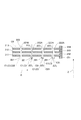
図2は、第1実施形態に係るイオン源105の断面模式図である。イオン源105は、ガス供給ライン120が接続された放電室201と、放電室201の周囲に配置された高周波コイルであるRFコイル202と、を備えている。   FIG. 2 is a schematic cross-sectional view of the ion source 105 according to the first embodiment. The ion source 105 includes a discharge chamber 201 to which a gas supply line 120 is connected, and an RF coil 202 that is a high-frequency coil disposed around the discharge chamber 201.

放電室201は、石英やセラミックなどの誘電体で構成された円筒形状の容器であり、円筒の一対の端面のうち一方が開口部であり、他方にはガス供給ライン120が接続されている。これにより、放電室201内には、ガス供給ライン120を通じて放電用ガスである酸素ガスが供給される。   The discharge chamber 201 is a cylindrical container made of a dielectric material such as quartz or ceramic. One of the pair of end faces of the cylinder is an opening, and the other is connected to a gas supply line 120. As a result, oxygen gas, which is a discharge gas, is supplied into the discharge chamber 201 through the gas supply line 120.

RFコイル202は、放電室201の他方の端面側に設けられた、スパイラル状のコイルであり、RF電源131及び整合器132により、高周波の電力が印加される。これにより、放電室201内のガスがプラズマPとなる。プラズマPは、イオンと電子に電離した状態である。プラズマPに含まれるイオンは、陽イオン、例えばO である。なお、RFコイル202は、放電室201の側面側に設けられた、ヘリカル状のコイルであってもよい。また、RFコイル202は、高周波電力の印加時に流れる電流により発熱するのを低減するため、RFコイル202内に冷却水を流すようにしてもよい。 The RF coil 202 is a spiral coil provided on the other end face side of the discharge chamber 201, and high frequency power is applied by the RF power supply 131 and the matching unit 132. Thereby, the gas in the discharge chamber 201 becomes plasma P. The plasma P is in a state of being ionized into ions and electrons. The ions contained in the plasma P are positive ions, for example, O 2 + . Note that the RF coil 202 may be a helical coil provided on the side of the discharge chamber 201. Further, the RF coil 202 may flow cooling water through the RF coil 202 in order to reduce heat generation due to a current flowing when high-frequency power is applied.

また、イオン源105は、放電室201の開口部側に設けられた、放電室201からイオンを引き出す複数(3つ)の電極211,212,213を備えている。放電室201から遠ざかる方向に向かって第1の電極である電極211、第2の電極である電極212、及び第3の電極である電極213が順に配置されている。イオン源105は、放電室201、RFコイル202及び電極211〜213が収容されるケース203を備えている。ケース203は、複数の電極211〜213のうち最外側に配置された電極213をケース203の外部に露出させる開口部を有する。つまり、複数の電極211〜213は、放電室201の開口部とケース203の開口部との間に配置されている。   The ion source 105 includes a plurality (three) of electrodes 211, 212, and 213 that are provided on the opening side of the discharge chamber 201 and extract ions from the discharge chamber 201. An electrode 211 that is a first electrode, an electrode 212 that is a second electrode, and an electrode 213 that is a third electrode are sequentially arranged in a direction away from the discharge chamber 201. The ion source 105 includes a case 203 in which the discharge chamber 201, the RF coil 202, and the electrodes 211 to 213 are accommodated. The case 203 has an opening that exposes the outermost electrode 213 of the plurality of electrodes 211 to 213 to the outside of the case 203. That is, the plurality of electrodes 211 to 213 are disposed between the opening of the discharge chamber 201 and the opening of the case 203.

電極211,212,213は、平板状、具体的には円板状の導体である。電極211,212,213は、モリブデンなどの耐腐食性に優れていた材料を用いるのが好ましい。電極211〜213を平板状としたことにより、湾曲した形状にするよりも加工が容易となり、電極211〜213を安価に製作することができ、ひいてはイオン源105を安価に製作することができる。   The electrodes 211, 212, and 213 are flat plate-shaped conductors, specifically, disk-shaped conductors. The electrodes 211, 212, and 213 are preferably made of a material having excellent corrosion resistance such as molybdenum. By making the electrodes 211 to 213 into a flat plate shape, the processing becomes easier than the curved shape, the electrodes 211 to 213 can be manufactured at low cost, and the ion source 105 can be manufactured at low cost.

ここで、電極211は、放電室201に最も近い位置に配置され、電極211よりも放電室201から遠い位置に電極212が配置され、電極212よりも放電室201から遠い位置に電極213が配置されている。電極211と電極212、電極212と電極213は所定の間隔をあけて配置されている。   Here, the electrode 211 is disposed at a position closest to the discharge chamber 201, the electrode 212 is disposed at a position farther from the discharge chamber 201 than the electrode 211, and the electrode 213 is disposed at a position farther from the discharge chamber 201 than the electrode 212. Has been. The electrode 211 and the electrode 212, and the electrode 212 and the electrode 213 are arranged at a predetermined interval.

放電室201と電極211との間、電極211と電極212との間、電極212と電極213との間、及び電極213とケース203との間には、それぞれ円環状の絶縁部材251,252,253,254が配置されている。具体的には、絶縁部材252は電極211の外周部と電極212の外周部との間に配置され、絶縁部材253は電極212の外周部と電極213の外周部との間に配置されている。絶縁部材251は電極211の外周部と放電室201の開口部の周囲との間に配置され、絶縁部材254は電極213の外周部とケース203の開口部の周囲との間に配置されている。絶縁部材251〜254は、例えば石英などの材料で構成されている。   Between the discharge chamber 201 and the electrode 211, between the electrode 211 and the electrode 212, between the electrode 212 and the electrode 213, and between the electrode 213 and the case 203, annular insulating members 251, 252, 253 and 254 are arranged. Specifically, the insulating member 252 is disposed between the outer periphery of the electrode 211 and the outer periphery of the electrode 212, and the insulating member 253 is disposed between the outer periphery of the electrode 212 and the outer periphery of the electrode 213. . The insulating member 251 is disposed between the outer periphery of the electrode 211 and the periphery of the opening of the discharge chamber 201, and the insulating member 254 is disposed between the outer periphery of the electrode 213 and the periphery of the opening of the case 203. . The insulating members 251 to 254 are made of a material such as quartz, for example.

絶縁部材251〜254により、放電室201内の中性ガスがケース203内に漏れるのを防止している。よって、RFコイル202に中性ガスが流れ込むのを防止することができ、ケース203内で放電するのを防止することができる。また、絶縁部材252,253により電極211と電極212、電極212と電極213の絶縁性を高めることができる。   The insulating members 251 to 254 prevent the neutral gas in the discharge chamber 201 from leaking into the case 203. Therefore, it is possible to prevent the neutral gas from flowing into the RF coil 202 and to prevent discharge in the case 203. Further, the insulating properties of the electrodes 211 and 212 and the electrodes 212 and 213 can be increased by the insulating members 252 and 253.

複数の電極211〜213は、図2に示すように、中心が軸線C0に一致している。つまり、電極211〜213の中心は軸線C0である。図2中、電極211〜213の平板面に垂直な方向、つまり平板面の法線方向は、Z方向である。電極211〜213は、平板面同士が互いに平行となるようにZ方向に並設されている。   As shown in FIG. 2, the centers of the plurality of electrodes 211 to 213 coincide with the axis C <b> 0. That is, the center of the electrodes 211 to 213 is the axis C0. In FIG. 2, the direction perpendicular to the flat plate surface of the electrodes 211 to 213, that is, the normal direction of the flat plate surface is the Z direction. The electrodes 211 to 213 are juxtaposed in the Z direction so that the flat plate surfaces are parallel to each other.

電極211は、第1の貫通孔である貫通孔221を複数有する。電極212は、第2の貫通孔である貫通孔222を複数有する。電極213は、第3の貫通孔である貫通孔223を複数有する。貫通孔222および貫通孔223は、貫通孔221と同じ数存在する。   The electrode 211 has a plurality of through holes 221 that are first through holes. The electrode 212 has a plurality of through holes 222 that are second through holes. The electrode 213 has a plurality of through holes 223 which are third through holes. The same number of through holes 222 and through holes 223 as the through holes 221 exist.

複数の貫通孔222の各々は、Z方向から見て、複数の貫通孔221の各々に一部又は全部が重なっている。つまり、貫通孔221と、この貫通孔221に相対する貫通孔222とは、Z方向から見て、一部又は全部が重なっている。また、貫通孔222と、この貫通孔222に相対する貫通孔223とは、Z方向から見て、一部又は全部が重なっている。これにより相対する貫通孔221,222,223は、イオンが通過するようにZ方向に連通している。放電室201内のイオンは、貫通孔221,222,223を通過することにより、イオンビームとなってホルダ102に保持されたワークWに照射される。貫通孔221〜223は、いかなる形状であってもよいが、Z方向から見て丸形状、つまり丸孔であるのが好ましい。各貫通孔221は、同一の大きさである。また、各貫通孔222は、同一の大きさである。また、各貫通孔223は、同一の大きさである。貫通孔221〜223同士も同一の大きさである。   Each of the plurality of through holes 222 partially or entirely overlaps each of the plurality of through holes 221 when viewed from the Z direction. That is, the through hole 221 and the through hole 222 opposite to the through hole 221 partially or entirely overlap when viewed from the Z direction. The through hole 222 and the through hole 223 opposite to the through hole 222 partially or entirely overlap when viewed from the Z direction. Thereby, the opposing through holes 221, 222, and 223 communicate with each other in the Z direction so that ions pass through. The ions in the discharge chamber 201 pass through the through holes 221, 222, and 223, and are irradiated to the workpiece W held in the holder 102 as an ion beam. The through holes 221 to 223 may have any shape, but are preferably round when viewed from the Z direction, that is, round holes. Each through hole 221 has the same size. Moreover, each through-hole 222 is the same size. Moreover, each through-hole 223 is the same size. The through holes 221 to 223 are also the same size.

第1実施形態では、電極211と電極213は貫通孔の配置が同じであり、電極211,213と電極212は貫通孔の配置が異なる。Z方向から見て複数の貫通孔223の各々は、複数の貫通孔221の各々と中心軸が一致して配置されている。これにより、複数の貫通孔223の各々は、相対する貫通孔221と全部が重なっている。なお、複数の貫通孔223の各々は、Z方向から見て相対する貫通孔222と一部又は全部と重なっている。   In the first embodiment, the electrode 211 and the electrode 213 have the same arrangement of the through holes, and the electrodes 211 and 213 and the electrode 212 have different arrangements of the through holes. As viewed from the Z direction, each of the plurality of through holes 223 is arranged such that the central axis thereof coincides with each of the plurality of through holes 221. Thereby, each of the plurality of through holes 223 entirely overlaps with the opposing through hole 221. Each of the plurality of through holes 223 overlaps part or all of the through holes 222 facing each other when viewed from the Z direction.

電極211には、電源装置261により、イオンの電荷と同じ極性の第1の電位である正電位が印加され、電極212には、電源装置262により、イオンの電荷と逆の極性の第2の電位である負電位が印加される。電極213は、接地されることにより、グラウンド電位となっている。   A positive potential which is a first potential having the same polarity as the charge of ions is applied to the electrode 211 by the power supply device 261, and a second potential having a polarity opposite to the charge of the ions is applied to the electrode 212 by the power supply device 262. A negative potential which is a potential is applied. The electrode 213 is grounded by being grounded.

電極211は、正電位が印加されることにより、放電室201から引き出されるイオンにエネルギーを与える。電極212は、負電位が印加されることにより、イオンを引き寄せて加速させる。電極213は、接地されることにより、真空容器101との電位差をなくす。   The electrode 211 imparts energy to ions extracted from the discharge chamber 201 by applying a positive potential. The electrode 212 is attracted and accelerated by applying a negative potential. The electrode 213 is grounded to eliminate a potential difference from the vacuum vessel 101.

図3は、第1実施形態に係るイオン源105の第2の電極である電極212を示す平面図である。図4は、第1実施形態に係るイオン源105の電極211〜213の一部の断面模式図である。   FIG. 3 is a plan view showing an electrode 212 that is the second electrode of the ion source 105 according to the first embodiment. FIG. 4 is a schematic cross-sectional view of a part of the electrodes 211 to 213 of the ion source 105 according to the first embodiment.

電極212の複数の貫通孔222は、Z方向から見て電極211の貫通孔221と一部が重なり、かつ電極211の貫通孔221に対して中心軸がずれて配置された貫通孔222Aを複数含んでいる。また、電極212の複数の貫通孔222は、電極211の貫通孔221と中心軸が一致して配置された貫通孔222Bを含んでいる。貫通孔222Bは、相対する貫通孔221と全部が重なっている。具体的に説明すると、貫通孔221の中心軸C1と貫通孔222Aの中心軸C21とがずれており、貫通孔221の中心軸C1と貫通孔222Bの中心軸C22とが一致している。なお、貫通孔221の中心軸C1と貫通孔223の中心軸C3とは一致している。貫通孔222Bは1つでもよいが、第1実施形態では複数存在する。即ち、複数の貫通孔222は、複数の貫通孔222Aと複数の貫通孔222Bとからなる。なお、複数の貫通孔222のうち、過半数が貫通孔222Aである。また、貫通孔222Aは、Z方向から見て相対する貫通孔223と一部が重なり、貫通孔222Bは、Z方向から見て相対する貫通孔223と全部が重なる。換言すると、複数の貫通孔223の各々は、Z方向から見て、相対する貫通孔222と一部又は全部が重なる。   The plurality of through-holes 222 of the electrode 212 partially include the plurality of through-holes 222 </ b> A that partially overlap with the through-hole 221 of the electrode 211 as viewed from the Z direction and are displaced from the central axis with respect to the through-hole 221 of the electrode 211. Contains. In addition, the plurality of through holes 222 of the electrode 212 include a through hole 222 </ b> B that is disposed so that the central axis coincides with the through hole 221 of the electrode 211. The through hole 222B entirely overlaps with the opposing through hole 221. Specifically, the central axis C1 of the through hole 221 and the central axis C21 of the through hole 222A are deviated, and the central axis C1 of the through hole 221 and the central axis C22 of the through hole 222B are coincident. The central axis C1 of the through hole 221 and the central axis C3 of the through hole 223 coincide with each other. Although there may be one through hole 222B, there are a plurality of through holes in the first embodiment. That is, the plurality of through holes 222 include a plurality of through holes 222A and a plurality of through holes 222B. The majority of the plurality of through holes 222 is the through hole 222A. Further, the through hole 222A partially overlaps with the through hole 223 that is opposed when viewed from the Z direction, and the through hole 222B entirely overlaps with the through hole 223 that is opposed when viewed from the Z direction. In other words, each of the plurality of through holes 223 partially or entirely overlaps the opposing through hole 222 when viewed from the Z direction.

貫通孔222Aが貫通孔221に対してずれて配置されることにより、電界レンズの効果で、貫通孔221,222Aを通過するイオンを偏向することができる。これにより、広範囲かつ均一にイオンを照射することが可能となる。即ち、イオンの照射領域を拡大し、照射領域におけるイオンの分布を均一化することが可能となる。   By disposing the through hole 222A with respect to the through hole 221, ions passing through the through holes 221 and 222A can be deflected by the effect of the electric field lens. Thereby, it becomes possible to irradiate ions uniformly in a wide range. That is, it is possible to enlarge the ion irradiation region and make the ion distribution uniform in the irradiation region.

貫通孔221に対する貫通孔222Aのずれ量及びずれ方向は、各電極における貫通孔の数及び位置に応じて設定すればよい。即ち、貫通孔222Aのずれ量及びずれ方向は、ホルダ102に保持された複数のワークWの全てにイオンが照射される照射領域となり、かつ照射領域内の各ワークWに均一にイオンが照射されるように設定すればよい。   What is necessary is just to set the deviation | shift amount and deviation | shift direction of 222 A of through-holes with respect to the through-hole 221 according to the number and position of the through-hole in each electrode. That is, the displacement amount and the displacement direction of the through-hole 222A become an irradiation region in which ions are irradiated to all of the plurality of workpieces W held by the holder 102, and each workpiece W in the irradiation region is uniformly irradiated with ions. It may be set so that.

第1実施形態では、電界レンズを効果的に発現させるため、貫通孔221に対する貫通孔222Aのずれ量は、貫通孔221の半径以下としている。即ち、貫通孔221の中心軸C1に対する貫通孔222Aの中心軸C21のずれ量ΔDは、貫通孔221の半径以下である。第1実施形態では、各貫通孔222Aのずれ量ΔDは一定としている。   In the first embodiment, the displacement amount of the through hole 222A with respect to the through hole 221 is set to be equal to or less than the radius of the through hole 221 in order to effectively develop the electric field lens. That is, the deviation ΔD of the central axis C21 of the through hole 222A with respect to the central axis C1 of the through hole 221 is equal to or less than the radius of the through hole 221. In the first embodiment, the shift amount ΔD of each through hole 222A is constant.

貫通孔222Bは、貫通孔222Aよりも電極212の中心C0の近くに配置されている。換言すると、貫通孔222Aは、貫通孔222Bよりも電極212の外周の近くに配置されている。中心C0に近い貫通孔222Bを通過するイオンは、ほとんど偏向せずZ方向に直進し、中心C0から遠い貫通孔222Aを通過するイオンは、Z方向に交差する方向に偏向する。電極212の外周側の貫通孔222Bを通過するイオンが偏向されるため、効果的にイオンの照射領域を拡大することができる。   The through hole 222B is disposed closer to the center C0 of the electrode 212 than the through hole 222A. In other words, the through hole 222A is disposed closer to the outer periphery of the electrode 212 than the through hole 222B. Ions passing through the through-hole 222B close to the center C0 go straight in the Z direction with little deflection, and ions passing through the through-hole 222A far from the center C0 are deflected in a direction intersecting the Z direction. Since ions passing through the through hole 222B on the outer peripheral side of the electrode 212 are deflected, the ion irradiation region can be effectively enlarged.

第1実施形態では、貫通孔221に対する貫通孔222Aのずれ方向は、中心C0から遠ざかる方向、即ち図3及び図4中、R方向である。これにより、貫通孔221,222Aを通過するイオンは、R方向に偏向され、よりイオンの照射領域を拡大することができる。   In the first embodiment, the displacement direction of the through hole 222A with respect to the through hole 221 is the direction away from the center C0, that is, the R direction in FIGS. Thereby, the ions passing through the through holes 221 and 222A are deflected in the R direction, and the irradiation region of the ions can be further enlarged.

また、Z方向から見て、複数の貫通孔222Bの総面積が、複数の貫通孔222Aの総面積よりも小さい。第1実施形態では、各貫通孔222A,222Bの開口面積が同一であるため、貫通孔222Bの数が、貫通孔222Aの数よりも少ない。よって、電極212の中心C0に近い貫通孔222Bを通過してワークWに到達するイオンの密度である電流密度が、貫通孔222Aを通過してワークWに到達するイオンの密度である電流密度よりも高くなるのを防止することができる。これにより、より効果的にホルダ102に保持された複数のワークWに均一にイオンを照射することができる。つまり、照射領域内に配置された複数のワークWに照射するイオンビームの電流密度分布をより均一にすることができる。   Further, as viewed from the Z direction, the total area of the plurality of through holes 222B is smaller than the total area of the plurality of through holes 222A. In the first embodiment, since the opening areas of the through holes 222A and 222B are the same, the number of the through holes 222B is smaller than the number of the through holes 222A. Therefore, the current density that is the density of ions that pass through the through-hole 222B near the center C0 of the electrode 212 and reaches the work W is greater than the current density that is the density of ions that pass through the through-hole 222A and reach the work W. Can also be prevented. Thereby, it is possible to irradiate the plurality of workpieces W held by the holder 102 more effectively with ions more effectively. That is, the current density distribution of the ion beam irradiated onto the plurality of workpieces W arranged in the irradiation region can be made more uniform.

なお、貫通孔222Bの総面積を、貫通孔222Aの総面積よりも小さくする構成として、各貫通孔222Bの開口面積を、各貫通孔222Aの開口面積よりも小さくしてもよい。この場合、貫通孔222Bに相対する貫通孔221の開口面積も、貫通孔222Aに相対する貫通孔221の開口面積よりも小さくすればよい。   In addition, you may make the opening area of each through-hole 222B smaller than the opening area of each through-hole 222A as a structure which makes the total area of through-hole 222B smaller than the total area of 222 A of through-holes. In this case, the opening area of the through hole 221 facing the through hole 222B may be smaller than the opening area of the through hole 221 facing the through hole 222A.

また、第1実施形態では、電極212に印加する負電位の絶対値が、電極211に印加する正電位の絶対値よりも大きい。これにより、電界レンズの効果を大きくすることができ、より広範囲にイオンを偏向させることが可能となる。   In the first embodiment, the absolute value of the negative potential applied to the electrode 212 is larger than the absolute value of the positive potential applied to the electrode 211. Thereby, the effect of the electric field lens can be increased, and ions can be deflected in a wider range.

また、各電極211〜213を平板状としたことにより、電極を湾曲させた場合のように電極間に余分な空間ができるのを防止することができ、RFコイル202に投入する高周波電力の効率を上げることが可能となる。   Further, since each of the electrodes 211 to 213 is formed in a flat plate shape, it is possible to prevent an extra space from being formed between the electrodes as in the case where the electrodes are bent, and the efficiency of the high frequency power input to the RF coil 202 is reduced. Can be raised.

以上、第1実施形態によれば、電界レンズ効果によりイオンビームの偏向が可能であり、広範囲にイオンビームを照射することが可能となる。また、イオンビームの電流密度分布を均一化することが可能となり、結果として、均一な膜質の薄膜を各ワークWに形成することができる。   As described above, according to the first embodiment, the ion beam can be deflected by the electric field lens effect, and the ion beam can be irradiated over a wide range. Further, the current density distribution of the ion beam can be made uniform, and as a result, a thin film having a uniform film quality can be formed on each workpiece W.

なお、第1実施形態では、図4に示すように、相対する貫通孔221と中心軸が一致する貫通孔222Bが存在しているが、貫通孔222Bが存在していなくてもよい。つまり、電極212の貫通孔の全てが、貫通孔221に対してずれて配置された貫通孔222Aであってもよい。   In the first embodiment, as shown in FIG. 4, the through hole 222 </ b> B whose center axis coincides with the opposing through hole 221 exists, but the through hole 222 </ b> B may not exist. That is, all of the through holes of the electrode 212 may be the through holes 222 </ b> A arranged so as to be shifted from the through holes 221.

[第2実施形態]
次に、第2実施形態に係るイオン源について説明する。図5は、第2実施形態に係るイオン源の第1〜第3の電極の一部の断面模式図である。なお、第2実施形態のイオン源において、第1実施形態のイオン源と同様の構成については、同一符号を付して説明を省略する。第2実施形態においても、イオン源は、第1の電極である電極211、第2の電極である電極212、第3の電極である電極213を備えている。
[Second Embodiment]
Next, an ion source according to the second embodiment will be described. FIG. 5 is a schematic cross-sectional view of a part of the first to third electrodes of the ion source according to the second embodiment. In addition, in the ion source of 2nd Embodiment, about the structure similar to the ion source of 1st Embodiment, the same code | symbol is attached | subjected and description is abbreviate | omitted. Also in the second embodiment, the ion source includes an electrode 211 that is a first electrode, an electrode 212 that is a second electrode, and an electrode 213 that is a third electrode.

第2実施形態では、図5に示すように、貫通孔221に対してずれて配置された貫通孔222Aは、電極212の中心C0に近いほどずれ量が小さい。即ち、中心C0に近いほどずれ量がΔD>ΔD>ΔDと小さくなる。これにより、より効果的に広範囲かつ均一にイオンを照射することが可能となる。 In the second embodiment, as shown in FIG. 5, the shift amount of the through hole 222 </ b> A that is shifted from the through hole 221 is smaller as it is closer to the center C <b> 0 of the electrode 212. That is, the closer to the center C0, the smaller the shift amount becomes ΔD 1 > ΔD 2 > ΔD 3 . Thereby, it becomes possible to irradiate ions more effectively in a wide range and uniformly.

なお、第2実施形態では、図5に示すように、相対する貫通孔221と中心軸が一致する貫通孔222Bが存在しているが、貫通孔222Bが存在していなくてもよい。つまり、電極212の貫通孔の全てが、貫通孔221に対してずれて配置された貫通孔222Aであってもよい。   In the second embodiment, as shown in FIG. 5, the through hole 222 </ b> B whose center axis coincides with the opposing through hole 221 exists, but the through hole 222 </ b> B may not exist. That is, all of the through holes of the electrode 212 may be the through holes 222 </ b> A arranged so as to be shifted from the through holes 221.

[実施例]
次に、上述したイオン源の実施例について説明する。本実施例のイオン源は、第1実施形態のイオン源の一例である。本実施例のイオン源において、電極211、電極212及び電極213の材料はモリブデンとした。各電極211,212,213の厚みを0.5[mm]、直径をφ70〜φ120[mm]とした。各電極211,212,213には、直径φ2[mm]、ピッチ距離2[mm]で貫通孔を加工した。
[Example]
Next, an example of the above-described ion source will be described. The ion source of the present example is an example of the ion source of the first embodiment. In the ion source of this example, the material of the electrode 211, the electrode 212, and the electrode 213 was molybdenum. The thickness of each electrode 211, 212, 213 was set to 0.5 [mm], and the diameter was set to φ70 to φ120 [mm]. Each electrode 211, 212, 213 was formed with a through hole with a diameter φ2 [mm] and a pitch distance 2 [mm].

電極212には、電極211,213に対して孔加工位置を0.5[mm]ずらして形成した。即ち、3つの電極211〜213を組み付けた際に、電極212の貫通孔222Aの中心軸が、電極211,213の貫通孔221,223の中心軸に対して0.5[mm]ずれるように形成した。   The electrode 212 was formed by shifting the hole processing position by 0.5 [mm] with respect to the electrodes 211 and 213. That is, when the three electrodes 211 to 213 are assembled, the central axis of the through hole 222A of the electrode 212 is shifted by 0.5 [mm] from the central axis of the through holes 221 and 223 of the electrodes 211 and 213. Formed.

電極211には、+300〜+600[V]の正電位を印加する電源装置261を接続した。電極212には、−800〜−1000[V]の負電位を印加する電源装置262を接続した。電極213は接地した。絶縁部材251〜254は、それぞれ内径φ120[mm]、外径φ160[mm]程度の石英リングとした。   A power supply device 261 that applies a positive potential of +300 to +600 [V] was connected to the electrode 211. A power supply device 262 that applies a negative potential of −800 to −1000 [V] was connected to the electrode 212. The electrode 213 was grounded. The insulating members 251 to 254 were quartz rings having an inner diameter of φ120 [mm] and an outer diameter of φ160 [mm], respectively.

ガス供給ライン120から放電用ガスとして酸素を供給する流量制御装置122は、10〜100[sccm]で酸素の流量を制御可能なものとした。RFコイル202は、3ターンのスパイラル状に線状の導体を巻いて構成した。RFコイル202に印加する高周波電力の周波数は13.56[MHz]とし、高周波電力の出力は200〜1000[W]の範囲とした。ここで、高周波電力の出力は、所望とするプラズマ密度に応じて調整した。   The flow rate control device 122 that supplies oxygen as a discharge gas from the gas supply line 120 can control the flow rate of oxygen at 10 to 100 [sccm]. The RF coil 202 was configured by winding a linear conductor in a three-turn spiral shape. The frequency of the high frequency power applied to the RF coil 202 was 13.56 [MHz], and the output of the high frequency power was in the range of 200 to 1000 [W]. Here, the output of the high frequency power was adjusted according to the desired plasma density.

なお、比較例のイオン源も用意した。比較例のイオン源においては、3つの電極の全てを実施例の電極211と同じ構成とし、電極間の貫通孔同士の中心軸が一致するように3つの電極を配置した。   A comparative ion source was also prepared. In the ion source of the comparative example, all the three electrodes have the same configuration as the electrode 211 of the example, and the three electrodes are arranged so that the central axes of the through holes between the electrodes coincide.

図6は、実施例及び比較例のイオン源を評価する評価装置300を示す模式図である。上記のように構成された実施例又は比較例のイオン源を、図6の評価装置300に搭載した。評価装置300は、電流を測定することでイオンビームの電流密度分布を把握可能に構成されている。   FIG. 6 is a schematic diagram illustrating an evaluation apparatus 300 that evaluates the ion sources of Examples and Comparative Examples. The ion source according to the example or the comparative example configured as described above was mounted on the evaluation apparatus 300 in FIG. The evaluation apparatus 300 is configured to be able to grasp the current density distribution of the ion beam by measuring the current.

評価装置300は、真空容器101と、真空容器101の内部に配置された測定用治具311とを備えている。測定用治具311は、外径φ900[mm]の傘状の部材を有する。傘状の部材の中心から半径方向に50[mm]、100[mm]、150[mm]、200[m]、250[mm]、300[mm]、350[mm]、400[mm]の箇所には、電流を測定可能な不図示の測定プローブがそれぞれ設置されている。   The evaluation apparatus 300 includes a vacuum vessel 101 and a measurement jig 311 arranged inside the vacuum vessel 101. The measurement jig 311 has an umbrella-shaped member having an outer diameter of φ900 [mm]. 50 [mm], 100 [mm], 150 [mm], 200 [m], 250 [mm], 300 [mm], 350 [mm], 400 [mm] in the radial direction from the center of the umbrella-shaped member A measurement probe (not shown) capable of measuring current is installed at each location.

以上の構成の評価装置300を用いて実験を行った。まず、補助排気系162により、真空容器101内の圧力が大気圧から100[Pa]程度になるまで排気を行った。次に主排気系161により、真空容器101内の圧力が2.0×10⁻²[Pa]以下となるまで排気を行った。 An experiment was performed using the evaluation apparatus 300 having the above configuration. First, exhaust was performed by the auxiliary exhaust system 162 until the pressure in the vacuum vessel 101 was changed from atmospheric pressure to about 100 [Pa]. Next, evacuation was performed by the main exhaust system 161 until the pressure in the vacuum vessel 101 became 2.0 × 10 −2 [Pa] or less.

次にガス供給ライン120から放電室201内に50[sccm]の酸素を導入し、RFコイル202に高周波電力を印加することで、イオン源の放電室201内に、プラズマPを生成した。プラズマPが生成された後、電極211に+450[V]、電極212に−1000[V]の電位を印加し、測定用治具311にイオンビームを照射した。RFコイル202に印加した高周波電力の初期値は400[W]とした。プラズマPを生成後は、所望のイオン電流量となるようにRFコイル202に印加する電力量を調整した。   Next, 50 [sccm] of oxygen was introduced from the gas supply line 120 into the discharge chamber 201, and high frequency power was applied to the RF coil 202 to generate plasma P in the discharge chamber 201 of the ion source. After the plasma P was generated, a potential of +450 [V] was applied to the electrode 211 and −1000 [V] was applied to the electrode 212, and the measurement jig 311 was irradiated with an ion beam. The initial value of the high frequency power applied to the RF coil 202 was 400 [W]. After the plasma P was generated, the amount of electric power applied to the RF coil 202 was adjusted so as to obtain a desired ion current amount.

図7は、実施例及び比較例のイオン源について、測定用治具311を用いて計測した電流密度分布を示すグラフである。電流密度分布の計測では、測定用治具311に照射される電流を測定し、断面積から電流密度分布を算出した。図7において、横軸は、測定用治具311の傘中心からの距離である。縦軸は、測定用治具311における電流密度分布(割合)である。なお、縦軸の基準(0%)は、測定用治具311の傘中心から50[mm]、100[mm]、150[mm]、200[mm]、250[mm]、300[mm]、350[mm]、400[mm]の位置での電流密度の最大値と最小値との中間値とした。図7に示すように、実施例のイオン源が比較例のイオン源に対して電流密度分布の均一性が改善することが確認できた。   FIG. 7 is a graph showing the current density distribution measured using the measurement jig 311 for the ion sources of the example and the comparative example. In the measurement of the current density distribution, the current irradiated to the measurement jig 311 was measured, and the current density distribution was calculated from the cross-sectional area. In FIG. 7, the horizontal axis represents the distance from the center of the umbrella of the measurement jig 311. The vertical axis represents the current density distribution (ratio) in the measurement jig 311. In addition, the reference | standard (0%) of a vertical axis | shaft is 50 [mm], 100 [mm], 150 [mm], 200 [mm], 250 [mm], 300 [mm] from the umbrella center of the measurement jig 311. , 350 [mm], and 400 [mm], the intermediate value between the maximum value and the minimum value of the current density. As shown in FIG. 7, it was confirmed that the uniformity of the current density distribution was improved in the ion source of the example with respect to the ion source of the comparative example.

次に、実施例と比較例のイオン源を蒸着装置100に搭載して成膜実験を行った結果について説明する。   Next, the results of film formation experiments performed by mounting the ion sources of Examples and Comparative Examples on the vapor deposition apparatus 100 will be described.

ホルダ102は傘状の部材であり、ホルダ102の傘中心から50[mm]、100[mm]、150[mm]、200[mm]、250[mm]、300[mm]、350[mm]、400[mm]の位置にそれぞれワークWを配置した。   The holder 102 is an umbrella-shaped member, and 50 [mm], 100 [mm], 150 [mm], 200 [mm], 250 [mm], 300 [mm], 350 [mm] from the umbrella center of the holder 102. , The workpiece W was arranged at a position of 400 [mm].

まず、蒸着装置100(図1参照)において、補助排気系162により真空容器101内の圧力が大気圧から100[Pa]程度になるまで荒引き排気を行った。次に主排気系161により真空容器101内の圧力を6.6×10⁻⁴[Pa]以下となるまで排気を行った。 First, in the vapor deposition apparatus 100 (see FIG. 1), roughing evacuation was performed by the auxiliary exhaust system 162 until the pressure in the vacuum vessel 101 became about 100 [Pa] from atmospheric pressure. Next, evacuation was performed by the main exhaust system 161 until the pressure in the vacuum vessel 101 became 6.6 × 10 −4 [Pa] or less.

次にヒータ103を250[℃]程度まで昇温させた。次に、電子発生装置106を起動し、電子発生装置106から電子を放出させ、RFコイル202に高周波を印加することで、放電室201内にプラズマPを生成した。放電室201内には50[sccm]の酸素を導入した。プラズマPの生成後、電極211に+450[V]、電極212に−1000[V]を印加した。またRFコイル202に印加した高周波電力の初期値は400[W]とした。プラズマPを生成後は、所望のイオン電流量となるようにRFコイル202に印加する電力量を調整した。   Next, the heater 103 was heated to about 250 [° C.]. Next, the electron generator 106 was started, electrons were emitted from the electron generator 106, and a high frequency was applied to the RF coil 202 to generate plasma P in the discharge chamber 201. 50 [sccm] of oxygen was introduced into the discharge chamber 201. After the plasma P was generated, +450 [V] was applied to the electrode 211 and −1000 [V] was applied to the electrode 212. The initial value of the high frequency power applied to the RF coil 202 was 400 [W]. After the plasma P was generated, the amount of electric power applied to the RF coil 202 was adjusted so as to obtain a desired ion current amount.

次にプロセスガスとして酸素を供給し、真空容器101内の圧力を2.0×10⁻²[Pa]に維持した。次に電子銃104Bにより蒸着材料Mを加熱した。蒸着材料Mが溶けて気化される状態まで加熱された後、シャッタ110を、不図示の機構により蒸着材料Mの直上より十分に離れた位置に移動させ、ワークW及びモニタ基板107に蒸着材料Mを堆積させた。ワークW及びモニタ基板107に蒸着材料Mを堆積させているときの蒸着レートは、水晶式膜厚計111によって計測され、所望の蒸着レートになるように電子銃104Bの電力供給量を制御した。 Next, oxygen was supplied as a process gas, and the pressure in the vacuum vessel 101 was maintained at 2.0 × 10 −2 [Pa]. Next, the vapor deposition material M was heated by the electron gun 104B. After the vapor deposition material M is heated to a state where it is melted and vaporized, the shutter 110 is moved to a position sufficiently away from immediately above the vapor deposition material M by a mechanism (not shown), and the vapor deposition material M is placed on the workpiece W and the monitor substrate 107. Was deposited. The vapor deposition rate when the vapor deposition material M was deposited on the workpiece W and the monitor substrate 107 was measured by the quartz film thickness meter 111, and the power supply amount of the electron gun 104B was controlled so as to obtain a desired vapor deposition rate.

ワークWに堆積された蒸着材料Mの膜厚は光学式膜厚計109によって計測され、所望の膜厚に達したとき、シャッタ110を不図示の機構により蒸着材料Mの直上まで移動させ、電子銃104Bの電力供給を停止した。   The film thickness of the vapor deposition material M deposited on the workpiece W is measured by the optical film thickness meter 109. When the desired film thickness is reached, the shutter 110 is moved to a position directly above the vapor deposition material M by a mechanism (not shown), The power supply of the gun 104B was stopped.

実施例のイオン源を適用した蒸着装置で形成された薄膜と、比較例のイオン源を適用した蒸着装置で形成された薄膜とを評価した。表1は、実施例及び比較例において形成された薄膜が所望の膜質を満たすか否かを示す表である。表1において、「○」は所望の膜質を満たしていることを示し、「×」は所望の膜質を満たしていないことを示す。   The thin film formed with the vapor deposition apparatus to which the ion source of an Example was applied, and the thin film formed with the vapor deposition apparatus to which the ion source of a comparative example was applied were evaluated. Table 1 is a table showing whether or not the thin films formed in the examples and comparative examples satisfy the desired film quality. In Table 1, “◯” indicates that the desired film quality is satisfied, and “X” indicates that the desired film quality is not satisfied.

Figure 2018073594
Figure 2018073594

表1に示すように、本実施例のイオン源を用いることで、広範囲のワークWに対して所望の膜質が得られることを確認した。   As shown in Table 1, it was confirmed that a desired film quality was obtained for a wide range of workpieces W by using the ion source of this example.

なお、本発明は、以上説明した実施形態及び実施例に限定されるものではなく、本発明の技術的思想内で多くの変形が可能である。また、実施形態及び実施例に記載された効果は、本発明から生じる最も好適な効果を列挙したに過ぎず、本発明による効果は、実施形態及び実施例に記載されたものに限定されない。   The present invention is not limited to the embodiments and examples described above, and many modifications are possible within the technical idea of the present invention. Further, the effects described in the embodiments and examples merely list the most preferable effects resulting from the present invention, and the effects according to the present invention are not limited to those described in the embodiments and examples.

上述した実施形態及び実施例では、イオン源を蒸着装置に適用した場合について説明したが、イオン源を適用する装置を蒸着装置に限定するものではない。イオン源を例えば薄膜をエッチングするエッチング装置に適用してもよい。   In the above-described embodiments and examples, the case where the ion source is applied to the vapor deposition apparatus has been described. However, the apparatus to which the ion source is applied is not limited to the vapor deposition apparatus. For example, the ion source may be applied to an etching apparatus for etching a thin film.

また、上述した実施形態及び実施例では、第1の電極の平板面に垂直な方向から見て、複数の第1の貫通孔と複数の第2の貫通孔とが全て重なる場合について説明したが、これに限定するものではない。第1の電極の平板面に垂直な方向から見て、複数の第1の貫通孔のうち、第2の貫通孔と重ならない貫通孔が存在していてもよいし、複数の第2の貫通孔のうち、第1の貫通孔と重ならない貫通孔が存在していてもよい。また、第1の貫通孔と第2の貫通孔とが同数である場合について説明したが、異なる数であってもよい。   In the above-described embodiments and examples, the case has been described in which the plurality of first through holes and the plurality of second through holes all overlap when viewed from the direction perpendicular to the flat surface of the first electrode. However, the present invention is not limited to this. There may be a through hole that does not overlap the second through hole among the plurality of first through holes when viewed from the direction perpendicular to the flat surface of the first electrode, or the plurality of second through holes Among the holes, there may be a through hole that does not overlap the first through hole. Moreover, although the case where the 1st through-hole and the 2nd through-hole are the same number was demonstrated, a different number may be sufficient.

同様に、上述した実施形態及び実施例では、第1の電極の平板面に垂直な方向から見て、複数の第2の貫通孔と複数の第3の貫通孔とが全て重なる場合について説明したが、これに限定するものではない。第1の電極の平板面に垂直な方向から見て、複数の第2の貫通孔のうち、第3の貫通孔と重ならない貫通孔が存在していてもよいし、複数の第3の貫通孔のうち、第2の貫通孔と重ならない貫通孔が存在していてもよい。また、第2の貫通孔と第3の貫通孔とが同数である場合について説明したが、異なる数であってもよい。   Similarly, in the above-described embodiments and examples, a case has been described in which the plurality of second through holes and the plurality of third through holes all overlap when viewed from the direction perpendicular to the flat surface of the first electrode. However, the present invention is not limited to this. There may be a through hole that does not overlap the third through hole among the plurality of second through holes when viewed from the direction perpendicular to the flat surface of the first electrode, or the plurality of third through holes Among the holes, there may be a through hole that does not overlap with the second through hole. Moreover, although the case where the 2nd through-hole and the 3rd through-hole are the same number was demonstrated, a different number may be sufficient.

また、上述した実施形態及び実施例では、複数の第3の貫通孔のうち、全てが第1の貫通孔と中心軸が一致する場合について説明したが、これに限定するものではない。複数の第3の貫通孔のうち、第1の貫通孔と中心軸が一致しない貫通孔が一部存在していてもよい。即ち、複数の第1の貫通孔のうち、第3の貫通孔と中心軸が一致しない貫通孔が一部存在していてもよい。また、第1の貫通孔と第3の貫通孔とが同数である場合について説明したが、異なる数であってもよい。   In the above-described embodiments and examples, the case where all of the plurality of third through holes coincide with the first through hole and the central axis is described, but the present invention is not limited to this. Among the plurality of third through holes, there may be a part of the through holes whose central axes do not coincide with the first through holes. That is, among the plurality of first through holes, there may be a part of the through holes whose central axes do not coincide with the third through holes. Moreover, although the case where the 1st through-hole and the 3rd through-hole are the same number was demonstrated, a different number may be sufficient.

100…蒸着装置、101…真空容器(チャンバ)、102…ホルダ、104…蒸発源、105…イオン源、201…放電室、211…電極(第1の電極)、212…電極(第2の電極)、213…電極(第3の電極)、221…貫通孔(第1の貫通孔)、222…貫通孔(第2の貫通孔)、222A…貫通孔(第1の貫通孔に対して中心軸がずれて配置された貫通孔)、222B…貫通孔(第1の貫通孔と中心軸が一致して配置された貫通孔)、223…貫通孔(第3の貫通孔) DESCRIPTION OF SYMBOLS 100 ... Vapor deposition apparatus, 101 ... Vacuum container (chamber), 102 ... Holder, 104 ... Evaporation source, 105 ... Ion source, 201 ... Discharge chamber, 211 ... Electrode (first electrode), 212 ... Electrode (second electrode) ) 213... Electrode (third electrode), 221... Through hole (first through hole), 222... Through hole (second through hole), 222 A. Through-holes arranged off-axis), 222B... Through-holes (through-holes arranged so that the central axis coincides with the first through-holes), 223... Through-holes (third through-holes)

Claims (13)

放電室と、
前記放電室からイオンを引き出す、平板状の第1の電極、及び前記第1の電極よりも前記放電室から遠い位置に配置された平板状の第2の電極と、を備え、
前記第1の電極は、複数の第1の貫通孔を有し、
前記第2の電極は、複数の第2の貫通孔を有し、
前記複数の第2の貫通孔は、前記第1の電極の平板面に垂直な方向から見て前記第1の貫通孔と一部が重なり、かつ前記第1の貫通孔に対して中心軸がずれて配置された貫通孔を複数含むことを特徴とするイオン源。
A discharge chamber;
A flat plate-like first electrode for extracting ions from the discharge chamber, and a flat plate-like second electrode arranged at a position farther from the discharge chamber than the first electrode,
The first electrode has a plurality of first through holes,
The second electrode has a plurality of second through holes,
The plurality of second through holes partially overlap with the first through hole when viewed from a direction perpendicular to the flat surface of the first electrode, and a central axis with respect to the first through hole. An ion source comprising a plurality of through holes arranged in a shifted manner.
前記第1の貫通孔に対して中心軸がずれて配置された貫通孔のずれ量が、前記第1の貫通孔の半径以下であることを特徴とする請求項1に記載のイオン源。   2. The ion source according to claim 1, wherein a shift amount of a through hole arranged with a center axis shifted with respect to the first through hole is equal to or less than a radius of the first through hole. 前記第1の貫通孔に対して中心軸がずれて配置された貫通孔が前記第2の電極の中心に近いほど、前記ずれ量が小さいことを特徴とする請求項2に記載のイオン源。   3. The ion source according to claim 2, wherein the shift amount is smaller as a through hole arranged with a center axis shifted from the first through hole is closer to the center of the second electrode. 前記第1の貫通孔に対して中心軸がずれて配置された貫通孔のずれ方向が、前記第2の電極の中心から遠ざかる方向であることを特徴とする請求項1乃至3のいずれか1項に記載のイオン源。   4. The shift direction of a through hole arranged with a center axis shifted with respect to the first through hole is a direction away from the center of the second electrode. 5. The ion source according to item. 前記複数の第2の貫通孔は、前記第1の貫通孔と中心軸が一致して配置された貫通孔を含むことを特徴とする請求項1乃至4のいずれか1項に記載のイオン源。   5. The ion source according to claim 1, wherein the plurality of second through holes include a through hole arranged so that a central axis thereof coincides with the first through hole. . 前記第1の貫通孔と中心軸が一致して配置された貫通孔は、前記第1の貫通孔に対して中心軸がずれて配置された貫通孔よりも前記第2の電極の中心の近くに配置されていることを特徴とする請求項5に記載のイオン源。   The through hole arranged so that the central axis coincides with the first through hole is closer to the center of the second electrode than the through hole arranged with the central axis shifted with respect to the first through hole. The ion source according to claim 5, wherein 前記平板面に垂直な方向から見て、前記第1の貫通孔と中心軸が一致して配置された貫通孔の総面積が、前記第1の貫通孔に対して中心軸がずれて配置された貫通孔の総面積よりも小さいことを特徴とする請求項5又は6に記載のイオン源。   When viewed from the direction perpendicular to the flat plate surface, the total area of the through holes arranged so that the central axis coincides with the first through hole is arranged so that the central axis is shifted from the first through hole. The ion source according to claim 5 or 6, wherein the ion source is smaller than a total area of the through holes. 前記第2の電極よりも前記放電室から遠い位置に配置された平板状の第3の電極を更に備え、
前記第3の電極は、複数の第3の貫通孔を有し、
前記複数の第3の貫通孔は、前記第1の電極の平板面に垂直な方向から見て前記第2の貫通孔と一部又は全部が重なり、かつ前記第1の貫通孔と中心軸が一致して配置された貫通孔を含むことを特徴とする請求項1乃至7のいずれか1項に記載のイオン源。
A flat plate-like third electrode disposed farther from the discharge chamber than the second electrode;
The third electrode has a plurality of third through holes,
The plurality of third through-holes partially or entirely overlap with the second through-hole when viewed from a direction perpendicular to the flat surface of the first electrode, and the first through-hole and the central axis are The ion source according to any one of claims 1 to 7, further comprising through-holes arranged to coincide with each other.
前記第1の電極には、前記イオンの電荷と同じ極性の第1の電位、前記第2の電極には、前記イオンの電荷と逆の極性の第2の電位を印加し、前記第3の電極を接地して、前記放電室から前記イオンを引き出すことを特徴とする請求項8に記載のイオン源。   A first potential having the same polarity as the charge of the ions is applied to the first electrode, and a second potential having a polarity opposite to the charge of the ions is applied to the second electrode. The ion source according to claim 8, wherein an electrode is grounded to extract the ions from the discharge chamber. 前記第2の電位の絶対値が、前記第1の電位の絶対値よりも大きいことを特徴とする請求項9に記載のイオン源。   The ion source according to claim 9, wherein an absolute value of the second potential is larger than an absolute value of the first potential. 前記イオンが陽イオンであり、
前記第1の電位が正電位、前記第2の電位が負電位であることを特徴とする請求項9又は10に記載のイオン源。
The ions are cations;
11. The ion source according to claim 9, wherein the first potential is a positive potential and the second potential is a negative potential.
前記第1の電極の外周部と前記第2の電極の外周部との間、及び前記第2の電極の外周部と前記第3の電極の外周部との間にそれぞれ配置された絶縁部材を更に備えたことを特徴とする請求項8乃至11のいずれか1項に記載のイオン源。   Insulating members disposed between the outer periphery of the first electrode and the outer periphery of the second electrode, and between the outer periphery of the second electrode and the outer periphery of the third electrode, respectively. The ion source according to claim 8, further comprising: チャンバと、
前記チャンバの内部に配置され、ワークを保持するホルダと、
前記ホルダに対向して配置された蒸発源と、
前記ホルダに対向して配置された請求項1乃至12のいずれか1項に記載のイオン源と、を備えたことを特徴とする蒸着装置。
A chamber;
A holder disposed inside the chamber and holding a workpiece;
An evaporation source disposed opposite the holder;
A vapor deposition apparatus comprising: the ion source according to claim 1 disposed opposite to the holder.
JP2016211042A 2016-10-27 2016-10-27 Ion source and vapor deposition apparatus Pending JP2018073594A (en)

Priority Applications (1)

Application Number Priority Date Filing Date Title
JP2016211042A JP2018073594A (en) 2016-10-27 2016-10-27 Ion source and vapor deposition apparatus

Applications Claiming Priority (1)

Application Number Priority Date Filing Date Title
JP2016211042A JP2018073594A (en) 2016-10-27 2016-10-27 Ion source and vapor deposition apparatus

Publications (1)

Publication Number Publication Date
JP2018073594A true JP2018073594A (en) 2018-05-10

Family

ID=62115484

Family Applications (1)

Application Number Title Priority Date Filing Date
JP2016211042A Pending JP2018073594A (en) 2016-10-27 2016-10-27 Ion source and vapor deposition apparatus

Country Status (1)

Country Link
JP (1) JP2018073594A (en)

Similar Documents

Publication Publication Date Title
US10998167B2 (en) Ion beam etch without need for wafer tilt or rotation
Burdovitsin et al. Fore-vacuum plasma-cathode electron sources
US6933508B2 (en) Method of surface texturizing
TWI428953B (en) Method and device for treating the surface of at least one part by using elementary plasma sources by electron cyclotron resonance
JP2021502688A (en) Radiofrequency plasma ion source of linearized energy
US20020144903A1 (en) Focused magnetron sputtering system
KR100642584B1 (en) Direct ion deposition method using ion beam sputtering and device for the same
KR101935090B1 (en) Ion bombardment device and method for using the same to clean substrate surface
JP2011179119A (en) Apparatus and method of physical vapor deposition with heat diffuser
JP2013139642A (en) Plasma treatment apparatus applied for sputtering film forming
US20070256927A1 (en) Coating Apparatus for the Coating of a Substrate and also Method for Coating
KR20120023035A (en) Film-forming method and film-forming apparatus
US20130333618A1 (en) Hall effect plasma source
EP2482303B1 (en) Deposition apparatus and methods
JP2020066800A (en) Plasma passage for high-capacity plasma cvd processing
JP4859523B2 (en) Plasma source, film forming apparatus and film manufacturing method
WO2011007830A1 (en) Film-forming apparatus
JP2006169630A (en) Method and apparatus for cathodic arc deposition of materials on a substrate
JP2018073594A (en) Ion source and vapor deposition apparatus
JP2021528815A (en) Single beam plasma source
JP3606842B2 (en) Electron gun and electron beam irradiation processing apparatus
JP4370949B2 (en) Deposition method
JP2011017088A (en) Plasma treatment apparatus for applying sputtering film deposition
RU2740146C1 (en) Ion source (ion gun)
JP7438853B2 (en) Magnetron sputtering equipment