JP2018063677A - Touch screen panel - Google Patents
Touch screen panel Download PDFInfo
- Publication number
- JP2018063677A JP2018063677A JP2016203034A JP2016203034A JP2018063677A JP 2018063677 A JP2018063677 A JP 2018063677A JP 2016203034 A JP2016203034 A JP 2016203034A JP 2016203034 A JP2016203034 A JP 2016203034A JP 2018063677 A JP2018063677 A JP 2018063677A
- Authority
- JP
- Japan
- Prior art keywords
- electrode
- transparent conductive
- conductive film
- touch screen
- screen panel
- Prior art date
- Legal status (The legal status is an assumption and is not a legal conclusion. Google has not performed a legal analysis and makes no representation as to the accuracy of the status listed.)
- Pending
Links
Images


Classifications
-
- G—PHYSICS
- G02—OPTICS
- G02F—OPTICAL DEVICES OR ARRANGEMENTS FOR THE CONTROL OF LIGHT BY MODIFICATION OF THE OPTICAL PROPERTIES OF THE MEDIA OF THE ELEMENTS INVOLVED THEREIN; NON-LINEAR OPTICS; FREQUENCY-CHANGING OF LIGHT; OPTICAL LOGIC ELEMENTS; OPTICAL ANALOGUE/DIGITAL CONVERTERS
- G02F1/00—Devices or arrangements for the control of the intensity, colour, phase, polarisation or direction of light arriving from an independent light source, e.g. switching, gating or modulating; Non-linear optics
- G02F1/01—Devices or arrangements for the control of the intensity, colour, phase, polarisation or direction of light arriving from an independent light source, e.g. switching, gating or modulating; Non-linear optics for the control of the intensity, phase, polarisation or colour
- G02F1/13—Devices or arrangements for the control of the intensity, colour, phase, polarisation or direction of light arriving from an independent light source, e.g. switching, gating or modulating; Non-linear optics for the control of the intensity, phase, polarisation or colour based on liquid crystals, e.g. single liquid crystal display cells
- G02F1/133—Constructional arrangements; Operation of liquid crystal cells; Circuit arrangements
- G02F1/1333—Constructional arrangements; Manufacturing methods
- G02F1/13338—Input devices, e.g. touch panels
-
- G—PHYSICS
- G06—COMPUTING; CALCULATING OR COUNTING
- G06F—ELECTRIC DIGITAL DATA PROCESSING
- G06F3/00—Input arrangements for transferring data to be processed into a form capable of being handled by the computer; Output arrangements for transferring data from processing unit to output unit, e.g. interface arrangements
- G06F3/01—Input arrangements or combined input and output arrangements for interaction between user and computer
- G06F3/03—Arrangements for converting the position or the displacement of a member into a coded form
- G06F3/041—Digitisers, e.g. for touch screens or touch pads, characterised by the transducing means
- G06F3/0416—Control or interface arrangements specially adapted for digitisers
-
- G—PHYSICS
- G06—COMPUTING; CALCULATING OR COUNTING
- G06F—ELECTRIC DIGITAL DATA PROCESSING
- G06F3/00—Input arrangements for transferring data to be processed into a form capable of being handled by the computer; Output arrangements for transferring data from processing unit to output unit, e.g. interface arrangements
- G06F3/01—Input arrangements or combined input and output arrangements for interaction between user and computer
- G06F3/03—Arrangements for converting the position or the displacement of a member into a coded form
- G06F3/041—Digitisers, e.g. for touch screens or touch pads, characterised by the transducing means
- G06F3/045—Digitisers, e.g. for touch screens or touch pads, characterised by the transducing means using resistive elements, e.g. a single continuous surface or two parallel surfaces put in contact
-
- G—PHYSICS
- G02—OPTICS
- G02F—OPTICAL DEVICES OR ARRANGEMENTS FOR THE CONTROL OF LIGHT BY MODIFICATION OF THE OPTICAL PROPERTIES OF THE MEDIA OF THE ELEMENTS INVOLVED THEREIN; NON-LINEAR OPTICS; FREQUENCY-CHANGING OF LIGHT; OPTICAL LOGIC ELEMENTS; OPTICAL ANALOGUE/DIGITAL CONVERTERS
- G02F1/00—Devices or arrangements for the control of the intensity, colour, phase, polarisation or direction of light arriving from an independent light source, e.g. switching, gating or modulating; Non-linear optics
- G02F1/01—Devices or arrangements for the control of the intensity, colour, phase, polarisation or direction of light arriving from an independent light source, e.g. switching, gating or modulating; Non-linear optics for the control of the intensity, phase, polarisation or colour
- G02F1/13—Devices or arrangements for the control of the intensity, colour, phase, polarisation or direction of light arriving from an independent light source, e.g. switching, gating or modulating; Non-linear optics for the control of the intensity, phase, polarisation or colour based on liquid crystals, e.g. single liquid crystal display cells
- G02F1/133—Constructional arrangements; Operation of liquid crystal cells; Circuit arrangements
- G02F1/1333—Constructional arrangements; Manufacturing methods
- G02F1/1343—Electrodes
-
- G—PHYSICS
- G02—OPTICS
- G02F—OPTICAL DEVICES OR ARRANGEMENTS FOR THE CONTROL OF LIGHT BY MODIFICATION OF THE OPTICAL PROPERTIES OF THE MEDIA OF THE ELEMENTS INVOLVED THEREIN; NON-LINEAR OPTICS; FREQUENCY-CHANGING OF LIGHT; OPTICAL LOGIC ELEMENTS; OPTICAL ANALOGUE/DIGITAL CONVERTERS
- G02F1/00—Devices or arrangements for the control of the intensity, colour, phase, polarisation or direction of light arriving from an independent light source, e.g. switching, gating or modulating; Non-linear optics
- G02F1/01—Devices or arrangements for the control of the intensity, colour, phase, polarisation or direction of light arriving from an independent light source, e.g. switching, gating or modulating; Non-linear optics for the control of the intensity, phase, polarisation or colour
- G02F1/13—Devices or arrangements for the control of the intensity, colour, phase, polarisation or direction of light arriving from an independent light source, e.g. switching, gating or modulating; Non-linear optics for the control of the intensity, phase, polarisation or colour based on liquid crystals, e.g. single liquid crystal display cells
- G02F1/133—Constructional arrangements; Operation of liquid crystal cells; Circuit arrangements
- G02F1/136—Liquid crystal cells structurally associated with a semi-conducting layer or substrate, e.g. cells forming part of an integrated circuit
- G02F1/1362—Active matrix addressed cells
- G02F1/136286—Wiring, e.g. gate line, drain line
-
- G—PHYSICS
- G06—COMPUTING; CALCULATING OR COUNTING
- G06F—ELECTRIC DIGITAL DATA PROCESSING
- G06F3/00—Input arrangements for transferring data to be processed into a form capable of being handled by the computer; Output arrangements for transferring data from processing unit to output unit, e.g. interface arrangements
- G06F3/01—Input arrangements or combined input and output arrangements for interaction between user and computer
- G06F3/03—Arrangements for converting the position or the displacement of a member into a coded form
- G06F3/041—Digitisers, e.g. for touch screens or touch pads, characterised by the transducing means
- G06F3/0412—Digitisers structurally integrated in a display
-
- G—PHYSICS
- G02—OPTICS
- G02F—OPTICAL DEVICES OR ARRANGEMENTS FOR THE CONTROL OF LIGHT BY MODIFICATION OF THE OPTICAL PROPERTIES OF THE MEDIA OF THE ELEMENTS INVOLVED THEREIN; NON-LINEAR OPTICS; FREQUENCY-CHANGING OF LIGHT; OPTICAL LOGIC ELEMENTS; OPTICAL ANALOGUE/DIGITAL CONVERTERS
- G02F1/00—Devices or arrangements for the control of the intensity, colour, phase, polarisation or direction of light arriving from an independent light source, e.g. switching, gating or modulating; Non-linear optics
- G02F1/01—Devices or arrangements for the control of the intensity, colour, phase, polarisation or direction of light arriving from an independent light source, e.g. switching, gating or modulating; Non-linear optics for the control of the intensity, phase, polarisation or colour
- G02F1/13—Devices or arrangements for the control of the intensity, colour, phase, polarisation or direction of light arriving from an independent light source, e.g. switching, gating or modulating; Non-linear optics for the control of the intensity, phase, polarisation or colour based on liquid crystals, e.g. single liquid crystal display cells
- G02F1/133—Constructional arrangements; Operation of liquid crystal cells; Circuit arrangements
- G02F1/1333—Constructional arrangements; Manufacturing methods
- G02F1/1335—Structural association of cells with optical devices, e.g. polarisers or reflectors
- G02F1/1336—Illuminating devices
- G02F1/133602—Direct backlight
Abstract
Description
本発明は、タッチスクリーンパネルに関する。 The present invention relates to a touch screen panel.
電子機器の表示部に対して直接入力することができるタッチスクリーンパネルが広く用いられている。このタッチスクリーンパネルは、ユーザが直接、表示部の画面に触れて操作するため、従来から静電気破壊に対する解決策として様々な技術が提案されている。例えば特許文献1は、透明導電膜の外周を囲むように、避雷針となる電極を配置することで、タッチスクリーンパネルを形成しているICやLSI等の静電気破壊を回避する技術を提案している。 A touch screen panel that can directly input to a display unit of an electronic device is widely used. Since this user operates the touch screen panel by directly touching the screen of the display unit, various techniques have been conventionally proposed as a solution to electrostatic breakdown. For example, Patent Document 1 proposes a technique for avoiding electrostatic breakdown of an IC, LSI, or the like forming a touch screen panel by arranging an electrode serving as a lightning rod so as to surround the outer periphery of the transparent conductive film. .
近年のタッチスクリーンパネルでは、小型化やデザイン性の観点から、狭額縁化が求められている。即ち、タッチスクリーンパネルの外形サイズを小さくしつつ、ユーザがタッチできる有効領域を広げることが求められている。しかしながら上記特許文献1に記載の技術では、避雷針用の電極をタッチスクリーンパネルの外周に配置する必要があるため、避雷針となる電極を配置しない場合に比べて、タッチスクリーンパネルの外形サイズが増大してしまうという課題がある。また、外形サイズを増大させずに避雷針となる電極を配置すると、タッチスクリーンパネルの有効領域が小さくなってしまうという課題がある。 In recent touch screen panels, a narrow frame is required from the viewpoint of miniaturization and design. That is, it is required to expand the effective area that can be touched by the user while reducing the external size of the touch screen panel. However, in the technique described in Patent Document 1, since it is necessary to arrange a lightning rod electrode on the outer periphery of the touch screen panel, the outer size of the touch screen panel increases as compared with the case where no lightning rod electrode is arranged. There is a problem that it ends up. In addition, when an electrode serving as a lightning rod is arranged without increasing the outer size, there is a problem that the effective area of the touch screen panel is reduced.
本発明の目的は、上記従来技術の課題を解決することにある。 An object of the present invention is to solve the above-described problems of the prior art.
本発明の目的は、タッチスクリーンパネルの狭額縁化と静電気破壊の対策を両立する技術を提供することにある。 An object of the present invention is to provide a technology that achieves both a narrow frame of a touch screen panel and a countermeasure against electrostatic breakdown.
上記目的を達成するために本発明の一態様に係るタッチスクリーンパネルは以下のような構成を備える。即ち、
表面に矩形の第1透明導電膜が形成されている第1電極基板と、
表面に矩形の第2透明導電膜が形成されている第2電極基板と、
前記第1電極基板の前記第1透明導電膜の対向する2つの辺に形成された第1及び第2電極部と、
前記第2電極基板の前記第2透明導電膜の対向する2つの辺に形成された第3及び第4電極部と、
前記第1及び第2電極基板に設けられ、前記第1及び第2電極部と、前記第3及び第4電極部とをそれぞれインターフェース回路と接続する接続部と、
前記第2電極基板の前記第3及び第4電極部の一方と対向する、前記第1電極基板の前記第1透明導電膜とは分離した有効領域の外に形成され、前記第1及び第2電極部の少なくともいずれかと接続された金属線と、を有し、
前記第1及び第2電極基板は、前記第1及び第2電極部と前記第3及び第4電極部とが方形配置となるように絶縁物を介して対向して接着されていることを特徴とする。
In order to achieve the above object, a touch screen panel according to an aspect of the present invention has the following configuration. That is,
A first electrode substrate having a rectangular first transparent conductive film formed on a surface thereof;
A second electrode substrate having a rectangular second transparent conductive film formed on the surface;
First and second electrode portions formed on two opposing sides of the first transparent conductive film of the first electrode substrate;
Third and fourth electrode portions formed on two opposing sides of the second transparent conductive film of the second electrode substrate;
A connecting portion provided on the first and second electrode substrates, for connecting the first and second electrode portions and the third and fourth electrode portions to an interface circuit, respectively;
The first and second electrode substrates are formed outside an effective region facing one of the third and fourth electrode portions of the second electrode substrate and separated from the first transparent conductive film of the first electrode substrate. A metal wire connected to at least one of the electrode parts,
The first and second electrode substrates are bonded to each other through an insulator so that the first and second electrode portions and the third and fourth electrode portions are in a square arrangement. And
本発明によれば、タッチした位置の検出に有効な第1電極基板の有効領域の外側に避雷針となる金属線を形成することにより、タッチスクリーンパネルの外形サイズに影響を与えることなく透明導電膜の静電気破壊を防止できる。 According to the present invention, the transparent conductive film is formed without affecting the outer size of the touch screen panel by forming the metal wire serving as the lightning rod outside the effective area of the first electrode substrate effective for detecting the touched position. Can prevent electrostatic breakdown.
本発明のその他の特徴及び利点は、添付図面を参照とした以下の説明により明らかになるであろう。尚、添付図面においては、同じ若しくは同様の構成には、同じ参照番号を付す。 Other features and advantages of the present invention will become apparent from the following description with reference to the accompanying drawings. In the accompanying drawings, the same or similar components are denoted by the same reference numerals.
添付図面は明細書に含まれ、その一部を構成し、本発明の実施形態を示し、その記述と共に本発明の原理を説明するために用いられる。
以下、添付図面を参照して本発明の実施形態を詳しく説明する。尚、以下の実施形態は特許請求の範囲に係る本発明を限定するものでなく、また本実施形態で説明されている特徴の組み合わせの全てが本発明の解決手段に必須のものとは限らない。 Hereinafter, embodiments of the present invention will be described in detail with reference to the accompanying drawings. The following embodiments do not limit the present invention according to the claims, and all combinations of features described in the embodiments are not necessarily essential to the solution means of the present invention. .
[実施形態1]
図1は、本発明の実施形態1に係る情報処理装置100の構成を例示するブロック図である。
[Embodiment 1]
FIG. 1 is a block diagram illustrating the configuration of the
情報処理装置100は、制御部101と操作部102を備えており、操作部102を介した情報の入出力が可能となっている。制御部101は、メインCPUやDRAM(いずれも不図示)を含んでおり、操作部のCPU111との通信や、表示部103に表示する描画データの作成や、タッチスクリーンコントローラ113からの座標データの認識を行う。
The
操作部102は、操作部制御基板110と、表示部103と、タッチスクリーンパネル104を備える。また操作部制御基板110は、CPU111と、デシリアライザ112と、タッチスクリーンコントローラ113を備える。CPU111は、表示部103のバックライト点灯制御や、図1に図示していない操作部制御基板110上の各種デバイスの制御を行う。デシリアライザ112は、制御部101からシリアル転送される描画データを、パラレル変換して表示部103に転送する。尚、表示部103の構成によっては、制御部101からシリアル転送された描画データを受信して表示することもできる。その場合、デシリアライザ112は不要である。タッチスクリーンコントローラ113は、ユーザがタッチスクリーンパネル104にタッチした際に、そのタッチスクリーンパネル104から送出されるアナログ座標データを、デジタルデータに変換して制御部101に転送する。表示部103は、実施形態1では、バックライトと液晶ディスプレイを含む表示部である。この表示部103は、後述するタッチスクリーンパネル104の下部に配置されることにより、ユーザが表示部103の表示を視認しながら、タッチスクリーンパネル104を直感的にタッチして、情報の入力や各種指示を行うことができる。タッチスクリーンパネル104は、抵抗膜方式のタッチスクリーンパネルであり、その詳細は後述する。タッチスクリーンI/F114は、タッチスクリーンパネル104とタッチスクリーンコントローラ113のインターフェース回路であり、配線やコネクタ、回路素子を含んでいる。その詳細は後述する。
The
図2は、実施形態1に係るタッチスクリーンパネル104のハードウェア構成を説明する分解斜視図である。
FIG. 2 is an exploded perspective view illustrating the hardware configuration of the
タッチスクリーンパネル104は、加飾フィルム201、上側電極基板202、下側電極基板203を有している。このタッチスクリーンパネル104は、表示部103の表示画面上に配置される。ユーザが、加飾フィルム201の上面から透視した表示画面に表示された指示に従って、指やペンなどで加飾フィルム201にタッチすることにより、そのタッチされた位置を検出する。ユーザがタッチすると、上側電極基板202と下側電極基板203の後述する透明導電膜同士が接触し、その接触した位置が示すアナログ座標データを、タッチスクリーンコントローラ113がデジタルデータに変換して制御部101へ転送する。これにより制御部101は、ユーザがタッチした位置のX及びY軸座標を取得することができる。
The
加飾フィルム201は、例えば、PET(Polyethylene terephthalate)製のフィルムである。加飾フィルム201は、下側電極基板203の下側に配置される表示部103の表示画面を見るための透明部204と、透明部204の周囲に設けられる所定幅の枠部205とを備えている。この枠部205は、例えば、所定の色又は模様等の加飾用の印刷を施した部分である。加飾フィルム201は、上側電極基板202の上側に配置されており、例えば粘着剤等で上側電極基板202に貼り付けられている。
The
上側電極基板202は、可撓性を有する上側透明絶縁基材206を備えており、上側透明絶縁基材206は、矩形の透明フィルムやガラス等の透明基板により形成されている。この上側透明絶縁基材206の下面の一部には、ITO(tin-doped indium oxide)等により上側透明導電膜207が形成される。この上側透明導電膜207のY軸方向の平行な2辺には、一対のX軸左電極部208とX軸右電極部209が形成される。更に、これら電極部208,209とは異なる一辺には、外部に引き出されるフレキシブル基板226の上側配線224,225と電極部208,209とを接続する接続部212,213を備える。ここで接続部212は、金属線210により電極部208と接続され、接続部213は、金属線211により電極部209と接続される。また、このフレキシブル基板226が接続された辺に対向する一辺には、静電気破壊を抑制するための金属線227が形成されていて、この金属線227はX軸右電極部209と接続されている。尚、ここで、これら電極部208,209、金属線210,211,227、及び接続部212,213は、銀ペーストを用いたスクリーン印刷により形成されている。
The
ここで、上側透明導電膜207を上側透明絶縁基材206の下面の一部に形成する際に、上側透明導電膜207を必要な箇所にだけパターンエッチングしている。そして、電極部208,209は、それぞれ上側透明導電膜207上に形成されていて、上側透明導電膜207と接続されている。また金属線210,211,227と接続部212,213の箇所には上側透明導電膜207が形成されず、これらが上側透明導電膜207と接触するのを防いでいる。
Here, when the upper transparent
尚、ここで、金属線227を除く、金属線210,211と接続部212,213の箇所には上側透明導電膜207のパターンエッチングを行わず、上側透明絶縁基材206の下面に形成することもできる。その場合、金属線210,211及び接続部212,213と上側透明導電膜207との間には、絶縁するための不図示のレジストを形成し、それぞれが上側透明導電膜207と接触するのを防ぐようにしても良い。
Here, the upper transparent
下側電極基板203は下側透明絶縁基材215を備えており、下側透明絶縁基材215は、矩形の透明フィルムやガラス等の透明基板により形成されている。下側透明絶縁基材215の上面の一部には、ITO(tin-doped indium oxide)等により下側透明導電膜216が形成される。下側透明導電膜216のX軸方向の平行な2辺には、一対のY軸下電極部217、Y軸上電極部218が形成される。更に、電極部217,218が設けられた2つの辺の内、上側電極基板202のフレキシブル基板226を接続する辺に対応する辺は、そのフレキシブル基板226の下側配線222,223と電極部217,218とを接続する接続部220,221を備える。ここでY軸上電極部218と接続部220とは直接接続され、Y軸下電極部217と接続部221とは金属線219により接続される。ここで、これら電極部217,218、金属線219、接続部220,221は、銀ペーストを用いたスクリーン印刷により形成されている。
The
ここでは、下側透明導電膜216を側透明絶縁基材215の上面の一部に形成する際に、下側透明導電膜216を必要な箇所にだけパターンエッチングしている。ここで電極部217,218は、それぞれ下側透明導電膜216上に形成されていて、下側透明導電膜216と接続されている。また金属線219と接続部220,221の箇所には、下側透明導電膜216が形成されず、これらが下側透明導電膜216と接触するのを防いでいる。また或いは、下側透明導電膜216のパターンエッチングを行わず、下側透明導電膜216の上面の全体に形成することもできる。その場合、金属線219及び接続部220,221と下側透明導電膜216との間には、絶縁するための不図示のレジストを形成し、それぞれが下側透明導電膜216と接触するのを防ぐようにしても良い。
Here, when the lower transparent
ここで上側透明導電膜207及び下側透明導電膜216間の空隙を確保するために、上側透明導電膜207及び下側透明導電膜216のいずれか一方の、これらが対向する表面に、絶縁性で微小寸法のドット状スペーサ228が、所定の間隔で形成される。そして、上側電極基板202と下側電極基板203とを粘着剤等により貼り合わせる。このとき、X軸の電極部208,209及びY軸の電極部217,218が方形配置となるように対向させ、各々の電極部を含む周縁部を、後述するレジストにより絶縁した状態にする。また或いは、上側のX軸の電極部208,209及び下側のY軸の電極部217,218は、レジストを使用せずに、絶縁性のスペーサを介して対向させ、各々の電極部とスペーサとを粘着剤等により貼り合わせても良い。併せて、フレキシブル基板226の上側配線224,225と接続部212,213、及びフレキシブル基板226の下側配線222,223と接続部220,221を、それぞれ接続する。
Here, in order to secure a gap between the upper transparent
ここで、上側電極基板202と下側電極基板203とを貼り合わせる際、静電気破壊を抑制するための金属線227とY軸下電極部217とが対向するように配置する。詳細には、加飾フィルム201のY軸下側の周縁部から金属線227までの距離が、加飾フィルム201のY軸下側の周縁部からY軸下電極部217までの距離より短くなるよう配置する。
Here, when the
尚、金属線227の箇所に対して、上側透明導電膜207のパターンエッチングが行われていないと、即ち、金属線227と上側透明導電膜207とが分離されていないと、金属線227に放電した際に、上側透明導電膜207がダメージを受ける。従って、金属線227の箇所のパターンエッチングは、併せて行う必要がある。
If the pattern of the upper transparent
本実施形態1では、加飾フィルム201のY軸下側の周縁部に静電気放電が発生した場合に、Y軸下電極部217に放電することによる下側透明導電膜216のダメージを防止するために、金属線227を避雷針として使用して、Y軸下電極部217への放電を防止している。
In the first embodiment, in order to prevent damage to the lower transparent
また金属線227は、タッチスクリーンパネル104上でタッチされた位置を検出するためには不要なものである。従来のタッチスクリーンパネルの上側透明絶縁基材では、この実施形態1に係る金属線227を形成した領域には金属線が存在せず、元々、有効領域の外側に位置している上側透明導電膜があるだけであった。従って、実施形態1に係る金属線227を形成しても、タッチした位置を検出するタッチ有効領域が狭くなることがなく、外形サイズにも影響を与えない。
Further, the
このように実施形態1によれば、タッチスクリーンパネル104の狭額縁化と静電気破壊対策を両立することができる。
As described above, according to the first embodiment, it is possible to achieve both narrowing of the frame of the
次に、実施形態1に係るタッチスクリーンパネル104の図2の断面A、断面B、断面C、断面Dについて、図3を参照して説明する。
Next, the cross-section A, cross-section B, cross-section C, and cross-section D of FIG. 2 of the
図3は、図2の断面A、断面B、断面C、断面Dの断面形状を示す断面図である。尚、図3において、図2と共通する箇所は同じ参照番号で示している。 FIG. 3 is a cross-sectional view showing the cross-sectional shapes of cross-section A, cross-section B, cross-section C, and cross-section D of FIG. In FIG. 3, portions common to FIG. 2 are denoted by the same reference numerals.
図3(A)は、図2で説明したタッチスクリーンパネル104の断面Aの断面図である。
FIG. 3A is a cross-sectional view of the cross-section A of the
加飾フィルム201と上側電極基板202とが粘着剤305で貼り付けられている。上側電極基板202には、上側透明絶縁基材206上の一部に上側透明導電膜207が形成されていて、上側透明導電膜207が形成されない箇所に、接続部213とX軸右電極部209とを接続する金属線211が形成されている。
The
また下側電極基板203では、下側透明絶縁基材215上の一部に下側透明導電膜216が形成されていて、下側透明導電膜216が形成されない箇所に、Y軸下電極部217と接続部221とを接続する金属線219が形成されている。また下側透明導電膜216にY軸上電極部218が接続されている。そして、上側電極基板202の金属線211と、下側電極基板203の金属線219及び下側Y軸電極部218のそれぞれには、絶縁するためのレジスト301,302が形成されていて、これらは粘着剤304で貼り合わされている。
Further, in the
図3(B)は、図2で説明したタッチスクリーンパネル104の断面Bの断面図である。
FIG. 3B is a cross-sectional view of the cross section B of the
加飾フィルム201と上側電極基板202とが粘着剤305で接着されている。上側電極基板202では、上側透明絶縁基材206上に上側透明導電膜207が形成されていて、上側透明導電膜207上にX軸右電極部209が接続されている。
The
一方、下側電極基板203には、下側透明絶縁基材215上の一部に下側透明導電膜216が形成されていて、下側透明導電膜216が形成されない箇所に、Y軸下電極部217と接続部221とを接続する金属線219が形成されている。そして上側電極基板202のX軸右電極部209と、下側電極基板203の金属線219上にはそれぞれ、絶縁するためのレジスト301,302が形成されていて、それらは粘着剤304で貼り合わされている。
On the other hand, in the
図3(C)は、図2で説明したタッチスクリーンパネル104の断面Cの断面図である。
FIG. 3C is a cross-sectional view of the cross section C of the
加飾フィルム201と上側電極基板202とが粘着剤305で貼り付けられている。上側電極基板202には、上側透明絶縁基材206上に上側透明導電膜207が形成されていて、上側透明導電膜207上にX軸左電極部208が接続されている。
The
また下側電極基板203では、下側透明絶縁基材215上に下側透明導電膜216が形成されている。そして、上側電極基板202のX軸左電極部208と、下側電極基板203の下側透明導電膜216のそれぞれには、絶縁するためのレジスト301,302が形成されていて、それらは粘着剤304で貼り合わせられている。
In the
図3(D)は、図2で説明したタッチスクリーンパネル104の断面Dの断面図である。
FIG. 3D is a cross-sectional view of the cross section D of the
加飾フィルム201と上側電極基板202とが粘着剤305で貼り付けられている。上側電極基板202には、上側透明絶縁基材206上の一部に上側透明導電膜207が形成されていて、上側透明導電膜207が形成されない箇所に、静電破壊を防止するための避雷針となる金属線227が形成されている。
The
また下側電極基板203では、下側透明絶縁基材215上に下側透明導電膜216が形成されていて、下側透明導電膜216上にY軸下電極部217が接続されている。そして上側電極基板202の上側透明導電膜207と、下側電極基板203のY軸下電極部217のそれぞれには、絶縁するためのレジスト(絶縁物)301,302が形成されていて、これらは粘着剤304で接着されている。
In the
図4は、実施形態1に係るタッチスクリーンI/F114の詳細構成を説明する図である。
FIG. 4 is a diagram illustrating a detailed configuration of the touch screen I /
配線222〜225は、図2で説明した、フレキシブル基板226に形成される信号線の配線を示し、これら信号線は、コネクタ405を介して操作部制御基板110と接続される。
The
フェライトビーズ406〜409は、各信号に混入するノイズ成分を除去するために実装される。TVS(Transient Voltage Suppressor)ダイオード410〜413は、静電気破壊からタッチスクリーンコントローラ113を保護するために実装される。配線222〜225を介して操作部制御基板110に流入した静電気は、一部がフェライトビーズ406〜409により除去される。更に、残りが、TVSダイオード410〜413を介してGND(接地)に逃がされることで、タッチスクリーンコントローラ113の破壊を防止している。
The
図5は、実施形態1に係るタッチスクリーンパネル104の額縁付近に静電気放電が発生した場合の放電経路を説明する断面図である。尚、図5において、前述の図3と共通する部分は同じ参照番号で示し、それらの説明は省略する。
FIG. 5 is a cross-sectional view illustrating a discharge path when electrostatic discharge is generated near the frame of the
図5(A)は、図2の断面A側の額縁付近で静電気放電が発生した場合の放電経路を説明する図である。放電された静電気は、経路500を辿って金属線211に帯電する。ここで上側透明導電膜207と金属線211は、図3(A)を参照して説明したようにエッチングにより分離されているため、上側透明導電膜207は静電気の影響を受けない。そして金属線211に帯電した静電気は、接続部213(図2)を介して操作部制御基板110に流入し、操作部制御基板110上のTVSダイオード413を介してGNDに逃がされる。
FIG. 5A is a diagram for explaining a discharge path when electrostatic discharge is generated near the frame on the cross-section A side in FIG. The discharged static electricity follows the
図5(B)は、図2の断面B側の額縁付近に静電気放電が発生した場合の放電経路を説明する図である。放電された静電気は、経路501を辿って上側透明導電膜207に帯電した後、経路502で示すように、よりインピーダンスの低いX軸右電極部209に流入する。この場合、上側透明導電膜207の一部は静電気によるダメージを受けるが、その部分はX軸右電極部209よりも外側の領域であるため、タッチスクリーンパネル104の有効座標外である。そのため問題無い。そしてX軸右電極部209に流入した静電気は、金属線211、接続部213を介して操作部制御基板110に流入し、操作部制御基板110上のTVSダイオード413を介してGNDに逃がされる。
FIG. 5B is a diagram illustrating a discharge path when electrostatic discharge is generated near the frame on the cross-section B side in FIG. The discharged static electricity follows the
図5(C)は、図2の断面C側の額縁付近に静電気放電が発生した場合の放電経路を説明する図である。放電された静電気は、経路503を辿って上側透明導電膜207に帯電した後、経路504で示すように、よりインピーダンスの低いX軸左電極部208に流入する。この場合、上側透明導電膜207の一部は静電気によるダメージを受けるが、その部分はX軸左電極部208よりも外側の領域であるため、タッチスクリーンパネル104の有効座標外である。そのため問題無い。そして、このX軸左電極部208に流入した静電気は、金属線210、接続部212(図2)を介して操作部制御基板110に流入し、操作部制御基板110上のTVSダイオード410を介してGNDに逃がされる。
FIG. 5C is a diagram illustrating a discharge path when electrostatic discharge is generated near the frame on the cross-section C side in FIG. The discharged static electricity follows the
図5(D)は、図2の断面D側の額縁付近に静電気放電が発生した場合の放電経路を説明する図である。放電された静電気は、経路505を辿って配線227に帯電する。上側透明導電膜207と金属線227は、前述した通りエッチングにより分離されているため、上側透明導電膜207は静電気の影響を受けない。そして金属線227に帯電した静電気は、電極部209及び接続部213を介して操作部制御基板110に流入し、操作部制御基板110のTVSダイオード413を介してGNDに逃がされる。
FIG. 5D is a diagram illustrating a discharge path when electrostatic discharge is generated near the frame on the cross-section D side in FIG. The discharged static electricity follows the
図5(E)は、本実施形態に係るタッチスクリーンパネルの効果を説明するため、従来のタッチスクリーンパネルにおける、図2の断面D側の額縁付近に静電気放電が発生した場合の放電経路に関して図示している。 FIG. 5E illustrates a discharge path when electrostatic discharge occurs in the vicinity of the frame on the cross-section D side of FIG. 2 in the conventional touch screen panel, in order to explain the effect of the touch screen panel according to the present embodiment. Show.
図5(E)では、図5(D)に示したような金属線227が存在しない。そのため、放電された静電気は、経路506を辿って上側透明導電膜207’に帯電した後、経路507で示すように、よりインピーダンスの低いY軸下電極部217’に2次放電する。この場合、上側透明導電膜207’の一部は静電気によるダメージを受けるが、その部分は電極部217’よりも外側の領域であるため、タッチスクリーンパネルの有効座標外である。そのため問題無い。一方、Y軸下電極部217’に帯電した静電気は、大部分がY軸下電極部217’及び金属線を介して操作部制御基板に流入する。こうして操作部制御基板に流入した静電気は、操作部制御基板のTVSダイオードを介してGNDに逃がされる。
In FIG. 5E, the
ここで注目すべきは、Y軸下電極部217’及び金属線を辿る経路長が長いことによるインピーダンスの増大が問題となり、経路508に示すように、静電気の一部が下側透明導電膜216’に流入してしまう可能性があることである。この場合、下側電極基板の下側透明導電膜216’の内、Y軸下電極部217’よりも内側の透明導電膜がダメージを受けることになり、タッチスクリーンパネルの有効座標が損傷するおそれがある。
It should be noted here that an increase in impedance due to a long path length following the Y-axis
これに対して図5(D)では、放電された静電気が金属線227に帯電して、電極部209及び接続部213を介して操作部制御基板110に流入するため、下側電極基板203のY軸下電極部217への2次放電を防止することができる。
On the other hand, in FIG. 5D, since the discharged static electricity is charged to the
また、金属線227の箇所がエッチングされて上側透明導電膜207と分離されているため、上側透明導電膜207への静電気の影響も防止できる。
Further, since the
尚、上記実施形態1では、図2の加飾フィルム201のY軸下側の周縁部に静電気放電が発生した場合に、Y軸下電極部217に放電することによる下側透明導電膜216のダメージを防止するために、金属線227を形成して避雷針として使用する例を説明した。ここで、避雷針は、Y軸下電極部217への放電を防げれば良く、金属線227がX軸右電極部209に接続される場合だけでなく、X軸左電極部208に接続されても良い。
In the first embodiment, when electrostatic discharge is generated at the peripheral edge on the Y axis lower side of the
[実施形態2]
上述の実施形態1では、タッチスクリーンパネル104の上側電極基板202及び下側電極基板203はともに矩形であり、X軸方向が長辺で、Y軸方向が短辺となっていて、フレキシブル基板226が、その長辺側に接続されていた。この場合、上側透明絶縁基材206のフレキシブル基板226と対向する辺に避雷針となる金属線227が形成されることで、Y軸下電極部217に静電気が放電することによる下側透明導電膜216のダメージを防止していた。
[Embodiment 2]
In the first embodiment described above, the
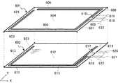
これに対して実施形態2では、図6のように、X軸方向が長辺で、Y軸方向が短辺となっている矩形のタッチスクリーンパネルにおいて、フレキシブル基板622が短辺側に接続されている場合で説明する。
On the other hand, in the second embodiment, as shown in FIG. 6, in a rectangular touch screen panel in which the X-axis direction is the long side and the Y-axis direction is the short side, the
図6は、本発明の実施形態2に係るタッチスクリーンパネル104のハードウェア構成を説明する分解斜視図である。このタッチスクリーンパネルは、上側電極基板601、下側電極基板602を有している。尚、加飾フィルム201は、前述の実施形態1に係る図2と同様に、上側電極基板601の上側に配置されているが、その構成は前述の実施形態1と同様であるため、その説明を省略する。
FIG. 6 is an exploded perspective view illustrating the hardware configuration of the
上側電極基板601は、可撓性を有する上側透明絶縁基材603を備えており、上側透明絶縁基材603は、矩形の透明フィルムやガラス等の透明基板により形成されている。上側透明絶縁基材603の下面の一部には、ITO(tin-doped indium oxide)等により上側透明導電膜604が形成される。そして、上側透明導電膜604のX軸方向に平行な2辺には、一対のY軸下電極部605とY軸上電極部606が形成される。更に、電極部605,606とは異なる1辺には、外部に引き出されるフレキシブル基板622の上側配線618,619と電極部605,606とを接続する接続部609,610を備える。ここで接続部609は、金属線607によりY軸下電極部605と接続され、接続部610は、金属線608によりY軸上電極部606と接続される。
The
また、フレキシブル基板622と対向する電極部605,606とは異なる一辺には、静電気破壊を抑制するための金属線624が形成されていて、金属線624はY軸下電極部605と接続されている。ここで、これら電極部605,606、金属線607,608、624、接続部609,610は、銀ペーストを用いたスクリーン印刷により形成されている。
Further, a
尚、図2の金属線227と同様に、金属線624の箇所で、上側透明導電膜604のパターンエッチングが行われていないと、静電気が金属線624に放電した際に、上側透明導電膜604がダメージを受けてしまう。従って、金属線604の箇所のパターンエッチングを併せて行うことにより、金属線624と上側透明導電膜604とを分離させる必要がある。
As in the case of the
下側電極基板602は、下側透明絶縁基材611を備えており、下側透明絶縁基材611は、矩形の透明フィルムやガラス等の透明基板により形成されている。下側透明絶縁基材611の上面の一部には、ITO(tin-doped indium oxide)等により下側透明導電膜612が形成される。この下側透明導電膜612のY軸方向の平行な2辺には、一対のX軸左電極部613、X軸右電極部614が形成される。更に、これら電極部613,614のうちの一辺には、外部に引き出されるフレキシブル基板622の下側配線620,621と電極部613,614とを接続する接続部616,617を備える。ここでX軸右電極部614と接続部617とは直接接続され、X軸左電極部613の一方の端部と接続部616とは、金属線615により接続される。尚、ここで、これらX軸左電極部613,X軸右電極部614、金属線615、接続部616,617は、銀ペーストを用いたスクリーン印刷により形成されている。
The
以上説明したように実施形態2に係るタッチスクリーンパネルでは、フレキシブル基板622がタッチスクリーンパネルの短辺側に接続される場合、フレキシブル基板226と対向する位置に避雷針となる金属線624を形成する。これにより放電された静電気が金属線624に帯電することにより、X軸左電極部613への放電を防止して、下側透明導電膜612のダメージを防止することができる。
As described above, in the touch screen panel according to the second embodiment, when the
[その他の実施形態]
上述の実施形態1,2では、加飾フィルム201が上側電極基板202の上側に配置されている場合で説明したが、タッチスクリーンパネルとして加飾フィルム201がない構成であっても、本発明は適用できる。つまり、上側電極基板202の周縁部に放電された静電気が、各電極部へと流入される構成であれば、金属線227により、Y軸下電極部217への放電を防止して、下側透明導電膜216の損傷を防止することができる。
[Other Embodiments]
In the first and second embodiments described above, the case where the
また実施形態2では、図2の加飾フィルム201のX軸左側の周縁部に静電気放電が発生した場合に、X軸下電極部613に放電することによる下側透明導電膜612のダメージを防止するために、金属線624を形成して避雷針として使用する例を説明した。
Moreover, in Embodiment 2, when electrostatic discharge generate | occur | produces in the peripheral part of the X-axis left side of the
ここで避雷針は、X軸下電極部613への放電を防げれば良く、金属線624がY軸下電極部605に接続される場合だけでなく、Y軸上電極部606に接続されても良い。
Here, the lightning rod only needs to prevent discharge to the X-axis
図7は、前述の実施形態1の変形例に係るタッチスクリーンパネル104のハードウェア構成を説明する分解斜視図である。ここでは前述の図2と共通する部分は同じ参照番号で示し、それらの説明を省略する。
FIG. 7 is an exploded perspective view illustrating the hardware configuration of the
図7では、金属線227に代えて、X軸左電極部208及びX軸右電極部209から伸びる金属線701及び702が設けられている。
In FIG. 7,
この場合は、金属線701及び702に帯電した静電気は、X軸左電極部208と接続部212、及びX軸右電極部209と接続部213を介して操作部制御基板110に流入する。そして、操作部制御基板110のTVSダイオード410,413を介してGNDに逃がされる。尚、これら金属線701及び702は、X軸左電極部208及びX軸右電極部209とは別体の金属線であっても良い。その場合、金属線701は、一方の電極部(X軸左電極部208)と接続され、金属線702は、他方の電極部(X軸右電極部209)と接続される。
In this case, static electricity charged in the
これらの避雷針の構成は、図6のようなフレキシブル基板622がタッチスクリーンパネルの短辺側に接続される場合でも同様である。
The structure of these lightning rods is the same even when the
また上述の実施形態では、タッチスクリーンパネル104の上側電極基板及び下側電極基板がともに長方形である場合で説明したが、これらの形状は正方形であってもよく、矩形の長さには制約されない。
In the above-described embodiment, the case where both the upper electrode substrate and the lower electrode substrate of the
本発明は上記実施形態に制限されるものではなく、本発明の精神及び範囲から離脱することなく、様々な変更及び変形が可能である。従って、本発明の範囲を公にするために、以下の請求項を添付する。 The present invention is not limited to the above-described embodiment, and various changes and modifications can be made without departing from the spirit and scope of the present invention. Therefore, in order to make the scope of the present invention public, the following claims are attached.
103…表示部、104…タッチスクリーンパネル、114…タッチスクリーンI/F、202…上側電極基板、203…下側電極基板、207…上側透明導電膜、208…X軸左電極部、209…X軸右電極部、216…下側透明導電膜、217…Y軸下電極部、218…Y軸上電極部、227,624…金属線
DESCRIPTION OF
Claims (7)
表面に矩形の第2透明導電膜が形成されている第2電極基板と、
前記第1電極基板の前記第1透明導電膜の対向する2つの辺に形成された第1及び第2電極部と、
前記第2電極基板の前記第2透明導電膜の対向する2つの辺に形成された第3及び第4電極部と、
前記第1及び第2電極基板に設けられ、前記第1及び第2電極部と、前記第3及び第4電極部とをそれぞれインターフェース回路と接続する接続部と、
前記第2電極基板の前記第3及び第4電極部の一方と対向する、前記第1電極基板の前記第1透明導電膜とは分離した有効領域の外に形成され、前記第1及び第2電極部の少なくともいずれかと接続された金属線と、を有し、
前記第1及び第2電極基板は、前記第1及び第2電極部と前記第3及び第4電極部とが方形配置となるように絶縁物を介して対向して接着されていることを特徴とするタッチスクリーンパネル。 A first electrode substrate having a rectangular first transparent conductive film formed on a surface thereof;
A second electrode substrate having a rectangular second transparent conductive film formed on the surface;
First and second electrode portions formed on two opposing sides of the first transparent conductive film of the first electrode substrate;
Third and fourth electrode portions formed on two opposing sides of the second transparent conductive film of the second electrode substrate;
A connecting portion provided on the first and second electrode substrates, for connecting the first and second electrode portions and the third and fourth electrode portions to an interface circuit, respectively;
The first and second electrode substrates are formed outside an effective region facing one of the third and fourth electrode portions of the second electrode substrate and separated from the first transparent conductive film of the first electrode substrate. A metal wire connected to at least one of the electrode parts,
The first and second electrode substrates are bonded to each other through an insulator so that the first and second electrode portions and the third and fourth electrode portions are in a square arrangement. Touch screen panel.
Priority Applications (3)
| Application Number | Priority Date | Filing Date | Title |
|---|---|---|---|
| JP2016203034A JP2018063677A (en) | 2016-10-14 | 2016-10-14 | Touch screen panel |
| US15/727,099 US20180107042A1 (en) | 2016-10-14 | 2017-10-06 | Touch screen panel |
| CN201710958278.3A CN107957810A (en) | 2016-10-14 | 2017-10-16 | Touch screen |
Applications Claiming Priority (1)
| Application Number | Priority Date | Filing Date | Title |
|---|---|---|---|
| JP2016203034A JP2018063677A (en) | 2016-10-14 | 2016-10-14 | Touch screen panel |
Publications (2)
| Publication Number | Publication Date |
|---|---|
| JP2018063677A true JP2018063677A (en) | 2018-04-19 |
| JP2018063677A5 JP2018063677A5 (en) | 2019-11-21 |
Family
ID=61902742
Family Applications (1)
| Application Number | Title | Priority Date | Filing Date |
|---|---|---|---|
| JP2016203034A Pending JP2018063677A (en) | 2016-10-14 | 2016-10-14 | Touch screen panel |
Country Status (3)
| Country | Link |
|---|---|
| US (1) | US20180107042A1 (en) |
| JP (1) | JP2018063677A (en) |
| CN (1) | CN107957810A (en) |
Cited By (3)
| Publication number | Priority date | Publication date | Assignee | Title |
|---|---|---|---|---|
| JP2019191791A (en) * | 2018-04-23 | 2019-10-31 | 富士通コンポーネント株式会社 | Touch panel device |
| JP2020149563A (en) * | 2019-03-15 | 2020-09-17 | 三菱電機株式会社 | Touch screen, touch panel, display device and electronic apparatus |
| CN112783352A (en) * | 2019-11-05 | 2021-05-11 | 江西慧光微电子有限公司 | Touch screen and preparation method thereof |
Families Citing this family (1)
| Publication number | Priority date | Publication date | Assignee | Title |
|---|---|---|---|---|
| WO2021060566A1 (en) * | 2019-09-26 | 2021-04-01 | キヤノン株式会社 | Image forming device |
Family Cites Families (11)
| Publication number | Priority date | Publication date | Assignee | Title |
|---|---|---|---|---|
| TWM351419U (en) * | 2008-10-13 | 2009-02-21 | Quanta Comp Inc | Electronic device and navigation device |
| US20110012845A1 (en) * | 2009-07-20 | 2011-01-20 | Rothkopf Fletcher R | Touch sensor structures for displays |
| US8755158B2 (en) * | 2012-05-01 | 2014-06-17 | Texas Instruments Incorporated | ESD protection system optimized at board level |
| KR102119600B1 (en) * | 2013-09-16 | 2020-06-08 | 엘지이노텍 주식회사 | Touch window |
| CN103500044B (en) * | 2013-09-30 | 2015-08-12 | 京东方科技集团股份有限公司 | Touch display panel and touch display unit |
| US9292141B2 (en) * | 2013-10-30 | 2016-03-22 | Apple Inc. | Double sided touch sensor on transparent substrate |
| JP6278708B2 (en) * | 2014-01-15 | 2018-02-14 | 富士通コンポーネント株式会社 | Touch panel |
| TWI524250B (en) * | 2014-05-20 | 2016-03-01 | 晨星半導體股份有限公司 | Touch control device and method, and touch device manufacturing method |
| US10061414B2 (en) * | 2014-10-22 | 2018-08-28 | Lg Innotek Co., Ltd. | Touch panel |
| CN105607769B (en) * | 2014-11-20 | 2018-10-26 | 宸鸿科技(厦门)有限公司 | Touch panel and the touch device with the touch panel |
| CN104808855A (en) * | 2015-04-30 | 2015-07-29 | 业成光电(深圳)有限公司 | Touch panel structure |
-
2016
- 2016-10-14 JP JP2016203034A patent/JP2018063677A/en active Pending
-
2017
- 2017-10-06 US US15/727,099 patent/US20180107042A1/en not_active Abandoned
- 2017-10-16 CN CN201710958278.3A patent/CN107957810A/en active Pending
Cited By (5)
| Publication number | Priority date | Publication date | Assignee | Title |
|---|---|---|---|---|
| JP2019191791A (en) * | 2018-04-23 | 2019-10-31 | 富士通コンポーネント株式会社 | Touch panel device |
| JP2020149563A (en) * | 2019-03-15 | 2020-09-17 | 三菱電機株式会社 | Touch screen, touch panel, display device and electronic apparatus |
| JP7308630B2 (en) | 2019-03-15 | 2023-07-14 | トライベイル テクノロジーズ, エルエルシー | Touch screens, touch panels, displays and electronics |
| CN112783352A (en) * | 2019-11-05 | 2021-05-11 | 江西慧光微电子有限公司 | Touch screen and preparation method thereof |
| CN112783352B (en) * | 2019-11-05 | 2022-10-11 | 江西卓讯微电子有限公司 | Touch screen and preparation method thereof |
Also Published As
| Publication number | Publication date |
|---|---|
| CN107957810A (en) | 2018-04-24 |
| US20180107042A1 (en) | 2018-04-19 |
Similar Documents
| Publication | Publication Date | Title |
|---|---|---|
| US11687204B2 (en) | Touch panel, display device, and electronic apparatus | |
| KR101693132B1 (en) | In-cell touch panel and display device | |
| KR101410584B1 (en) | Touch panel and a manufacturing method thereof | |
| WO2018010370A1 (en) | Touch substrate, touch display apparatus having the same, and fabricating method | |
| US20140098304A1 (en) | Touch screen panel | |
| EP3229111A1 (en) | Touch substrate, touch panel and display device | |
| US20170277308A1 (en) | Capacitive touch screen and method of manufacturing the same and touch control device | |
| US10845636B2 (en) | Input detection device | |
| JP2018063677A (en) | Touch screen panel | |
| JP2016212766A (en) | Touch screen, touch panel, display device, and electronic apparatus | |
| US20140092023A1 (en) | Touch display module and handheld electronic apparatus | |
| JP2018112791A (en) | Touch detection device and display device with touch detection function | |
| KR101548014B1 (en) | Capacitive touch sensing structure, process of producing the same and touch sensing device using the same | |
| US9760230B2 (en) | Touch screen, touch panel, display device, and electronic device | |
| US10185437B2 (en) | Touch screen panel, interface circuit, and information processing apparatus | |
| JP2015210554A (en) | Touch screen, touch panel, display device, and electronic apparatus | |
| CN110888558B (en) | Touch panel and touch device | |
| JP2018112842A (en) | Touch panel sensor and display with touch position detection function | |
| CN107608554B (en) | Touch sensing structure | |
| WO2019041920A1 (en) | Touch-control display panel | |
| US20180143719A1 (en) | Touch panel and display device using same | |
| CN109032425B (en) | Touch control display panel | |
| JP6576080B2 (en) | Capacitive touch panel | |
| KR101960055B1 (en) | Touch Sensor And Display Device | |
| EP2746902A1 (en) | Touch-sensitive device and touch-sensitive display device |
Legal Events
| Date | Code | Title | Description |
|---|---|---|---|
| A521 | Request for written amendment filed |
Free format text: JAPANESE INTERMEDIATE CODE: A523 Effective date: 20191007 |
|
| A621 | Written request for application examination |
Free format text: JAPANESE INTERMEDIATE CODE: A621 Effective date: 20191007 |
|
| A131 | Notification of reasons for refusal |
Free format text: JAPANESE INTERMEDIATE CODE: A131 Effective date: 20200601 |
|
| A977 | Report on retrieval |
Free format text: JAPANESE INTERMEDIATE CODE: A971007 Effective date: 20200529 |
|
| A02 | Decision of refusal |
Free format text: JAPANESE INTERMEDIATE CODE: A02 Effective date: 20210104 |
|
| RD01 | Notification of change of attorney |
Free format text: JAPANESE INTERMEDIATE CODE: A7421 Effective date: 20210103 |
|
| A521 | Request for written amendment filed |
Free format text: JAPANESE INTERMEDIATE CODE: A523 Effective date: 20210113 |