JP2018018513A - Memory system, processing system, and method for operating memory stacks - Google Patents
Memory system, processing system, and method for operating memory stacks Download PDFInfo
- Publication number
- JP2018018513A JP2018018513A JP2017110782A JP2017110782A JP2018018513A JP 2018018513 A JP2018018513 A JP 2018018513A JP 2017110782 A JP2017110782 A JP 2017110782A JP 2017110782 A JP2017110782 A JP 2017110782A JP 2018018513 A JP2018018513 A JP 2018018513A
- Authority
- JP
- Japan
- Prior art keywords
- memory
- instruction
- tag
- value
- address
- Prior art date
- Legal status (The legal status is an assumption and is not a legal conclusion. Google has not performed a legal analysis and makes no representation as to the accuracy of the status listed.)
- Pending
Links
Images


Classifications
-
- G—PHYSICS
- G06—COMPUTING; CALCULATING OR COUNTING
- G06F—ELECTRIC DIGITAL DATA PROCESSING
- G06F13/00—Interconnection of, or transfer of information or other signals between, memories, input/output devices or central processing units
- G06F13/38—Information transfer, e.g. on bus
- G06F13/40—Bus structure
-
- G—PHYSICS
- G06—COMPUTING; CALCULATING OR COUNTING
- G06F—ELECTRIC DIGITAL DATA PROCESSING
- G06F12/00—Accessing, addressing or allocating within memory systems or architectures
- G06F12/02—Addressing or allocation; Relocation
- G06F12/08—Addressing or allocation; Relocation in hierarchically structured memory systems, e.g. virtual memory systems
- G06F12/10—Address translation
- G06F12/1027—Address translation using associative or pseudo-associative address translation means, e.g. translation look-aside buffer [TLB]
- G06F12/1045—Address translation using associative or pseudo-associative address translation means, e.g. translation look-aside buffer [TLB] associated with a data cache
-
- G—PHYSICS
- G06—COMPUTING; CALCULATING OR COUNTING
- G06F—ELECTRIC DIGITAL DATA PROCESSING
- G06F12/00—Accessing, addressing or allocating within memory systems or architectures
- G06F12/02—Addressing or allocation; Relocation
- G06F12/08—Addressing or allocation; Relocation in hierarchically structured memory systems, e.g. virtual memory systems
- G06F12/0802—Addressing of a memory level in which the access to the desired data or data block requires associative addressing means, e.g. caches
- G06F12/0862—Addressing of a memory level in which the access to the desired data or data block requires associative addressing means, e.g. caches with prefetch
-
- G—PHYSICS
- G06—COMPUTING; CALCULATING OR COUNTING
- G06F—ELECTRIC DIGITAL DATA PROCESSING
- G06F12/00—Accessing, addressing or allocating within memory systems or architectures
- G06F12/02—Addressing or allocation; Relocation
- G06F12/0223—User address space allocation, e.g. contiguous or non contiguous base addressing
- G06F12/0292—User address space allocation, e.g. contiguous or non contiguous base addressing using tables or multilevel address translation means
-
- G—PHYSICS
- G06—COMPUTING; CALCULATING OR COUNTING
- G06F—ELECTRIC DIGITAL DATA PROCESSING
- G06F12/00—Accessing, addressing or allocating within memory systems or architectures
- G06F12/02—Addressing or allocation; Relocation
- G06F12/08—Addressing or allocation; Relocation in hierarchically structured memory systems, e.g. virtual memory systems
- G06F12/0802—Addressing of a memory level in which the access to the desired data or data block requires associative addressing means, e.g. caches
- G06F12/0893—Caches characterised by their organisation or structure
-
- G—PHYSICS
- G06—COMPUTING; CALCULATING OR COUNTING
- G06F—ELECTRIC DIGITAL DATA PROCESSING
- G06F2212/00—Indexing scheme relating to accessing, addressing or allocation within memory systems or architectures
- G06F2212/10—Providing a specific technical effect
- G06F2212/1016—Performance improvement
- G06F2212/1024—Latency reduction
-
- G—PHYSICS
- G06—COMPUTING; CALCULATING OR COUNTING
- G06F—ELECTRIC DIGITAL DATA PROCESSING
- G06F2212/00—Indexing scheme relating to accessing, addressing or allocation within memory systems or architectures
- G06F2212/60—Details of cache memory
- G06F2212/6028—Prefetching based on hints or prefetch instructions
-
- G—PHYSICS
- G11—INFORMATION STORAGE
- G11C—STATIC STORES
- G11C2207/00—Indexing scheme relating to arrangements for writing information into, or reading information out from, a digital store
- G11C2207/10—Aspects relating to interfaces of memory device to external buses
- G11C2207/107—Serial-parallel conversion of data or prefetch
-
- G—PHYSICS
- G11—INFORMATION STORAGE
- G11C—STATIC STORES
- G11C2211/00—Indexing scheme relating to digital stores characterized by the use of particular electric or magnetic storage elements; Storage elements therefor
- G11C2211/56—Indexing scheme relating to G11C11/56 and sub-groups for features not covered by these groups
- G11C2211/564—Miscellaneous aspects
- G11C2211/5643—Multilevel memory comprising cache storage devices
-
- Y—GENERAL TAGGING OF NEW TECHNOLOGICAL DEVELOPMENTS; GENERAL TAGGING OF CROSS-SECTIONAL TECHNOLOGIES SPANNING OVER SEVERAL SECTIONS OF THE IPC; TECHNICAL SUBJECTS COVERED BY FORMER USPC CROSS-REFERENCE ART COLLECTIONS [XRACs] AND DIGESTS
- Y02—TECHNOLOGIES OR APPLICATIONS FOR MITIGATION OR ADAPTATION AGAINST CLIMATE CHANGE
- Y02D—CLIMATE CHANGE MITIGATION TECHNOLOGIES IN INFORMATION AND COMMUNICATION TECHNOLOGIES [ICT], I.E. INFORMATION AND COMMUNICATION TECHNOLOGIES AIMING AT THE REDUCTION OF THEIR OWN ENERGY USE
- Y02D10/00—Energy efficient computing, e.g. low power processors, power management or thermal management
Landscapes
- Engineering & Computer Science (AREA)
- Theoretical Computer Science (AREA)
- General Engineering & Computer Science (AREA)
- Physics & Mathematics (AREA)
- General Physics & Mathematics (AREA)
- Computer Hardware Design (AREA)
- Memory System Of A Hierarchy Structure (AREA)
Abstract
Description
本発明は高帯域幅メモリに係り、より詳細には、高帯域幅メモリをキャッシュメモリとして使用するためのメモリシステム、プロセシングシステム、及びメモリスタックを動作させる方法に関する。 The present invention relates to a high bandwidth memory, and more particularly to a memory system, a processing system, and a method of operating a memory stack for using the high bandwidth memory as a cache memory.
HBM(High Bandwidth Memory、高帯域幅メモリ)は3次元スタック式ダイナミックRAM(DRAM)のための高性能RAMインターフェイスとして作用する。HBMをキャッシュメモリとして使用する従来の関連技術システムは、ホスト上にキャッシュ管理部を有し、キャッシュ管理機能を遂行する。このような配置はホストと、ホスト及びHBMの間のインターフェイスとに負担をかける恐れがある。 HBM (High Bandwidth Memory) acts as a high performance RAM interface for 3D stacked dynamic RAM (DRAM). The related art system using the HBM as a cache memory has a cache management unit on the host and performs a cache management function. Such an arrangement can place a burden on the host and the interface between the host and the HBM.
したがって、HBMをキャッシュメモリとして使用する際にはシステム及び方法の改革が必要である。 Therefore, when the HBM is used as a cache memory, it is necessary to reform the system and method.
本発明の目的は高帯域幅メモリをキャッシュメモリとして使用するためのシステム及び方法を提供することにある。 It is an object of the present invention to provide a system and method for using a high bandwidth memory as a cache memory.
本発明の一実施形態に係る実施形態の1つ以上の側面は、高帯域幅メモリをキャッシュメモリとして使用するためのシステム及び方法に対するものである。高帯域幅メモリはロジックダイ及びロジックダイ上にスタッキングされた、複数のDRAMダイを含む。ロジックダイはキャッシュ管理部を含み、キャッシュ管理部はJESD235A標準に適合する外部インターフェイスを通じて外部システムとインターフェイスし、アドレス変換機、命令変換機、及びタッグ比較器を含むことができる。アドレス変換機は外部インターフェイスを通じて受信された各々の物理的アドレスをタッグ値、メモリダイスタック内のタッグアドレス、及びメモリダイスタック内のデータアドレスに変換する。タッグ比較器はアドレス変換機によって生成されるタッグ値がタッグアドレスに格納されたタッグ値と同一であるか否かによってキャッシュヒット及びキャッシュミスが発生したか否かを判別する。命令生成器は命令を生成させる。例えば、外部インターフェイスを通じての書込み命令の受信にしたがって、命令生成器は先ず命令を生成し、タッグ値をフェッチして、キャッシュヒットが発生したか否かを判断し、そしてキャッシュヒットが発生した場合、命令生成器は書込み命令を生成させる。 One or more aspects of an embodiment according to an embodiment of the invention are directed to a system and method for using a high bandwidth memory as a cache memory. A high bandwidth memory includes a logic die and a plurality of DRAM dies stacked on the logic die. The logic die includes a cache management unit that interfaces with an external system through an external interface that conforms to the JESD235A standard and can include an address translator, an instruction translator, and a tag comparator. The address translator converts each physical address received through the external interface into a tag value, a tag address in the memory die stack, and a data address in the memory die stack. The tag comparator determines whether a cache hit or a cache miss has occurred depending on whether the tag value generated by the address translator is the same as the tag value stored in the tag address. The instruction generator causes an instruction to be generated. For example, upon receipt of a write instruction through an external interface, the instruction generator first generates an instruction, fetches a tag value to determine whether a cache hit has occurred, and if a cache hit has occurred, The instruction generator causes a write instruction to be generated.
本発明の一実施形態にしたがって提供されるメモリシステムは複数のメモリダイを含むメモリスタック、ロジックダイを含み、前記メモリダイは前記ロジックダイ上にスタッキングされ、前記ロジックダイに連結され、前記ロジックダイは前記メモリシステムに対する外部インターフェイスを具備し、前記ロジックダイは、前記メモリシステムに対する外部インターフェイス、キャッシュ管理部を含む。 A memory system provided in accordance with an embodiment of the present invention includes a memory stack including a plurality of memory dies, a logic die, the memory dies stacked on the logic die, and coupled to the logic die. An external interface for the memory system is provided, and the logic die includes an external interface for the memory system and a cache management unit.
一実施形態において、前記キャッシュ管理部は前記外部インターフェイスを通じて受信されたアドレスを変換して第1タッグ値、前記メモリスタックのデータアドレス、及び前記メモリスタックのタッグアドレスを生成するアドレス変換機(translator)を含む。 In one embodiment, the cache management unit converts an address received through the external interface to generate a first tag value, a data address of the memory stack, and a tag address of the memory stack. including.
一実施形態において、前記キャッシュ管理部は前記外部インターフェイスを通じて受信される読出し命令に応答してタッグをフェッチする第1命令及びデータワードをフェッチする第2命令を生成する命令変換機を含む。 In one embodiment, the cache manager includes an instruction converter that generates a first instruction to fetch a tag and a second instruction to fetch a data word in response to a read instruction received through the external interface.
一実施形態において、前記キャッシュ管理部はキャッシュヒット信号を生成させるタッグ比較器を含み、前記キャッシュヒット信号は前記第1タッグ値が前記第1命令の実行の結果値と同一である場合、真値を有し、前記第1タッグ値が前記第1命令の実行の結果値と同一でない場合、偽値を有する。 In one embodiment, the cache management unit includes a tag comparator that generates a cache hit signal, and the cache hit signal has a true value when the first tag value is the same as a result value of the execution of the first instruction. And if the first tag value is not the same as the result value of the execution of the first instruction, it has a false value.
一実施形態において、前記タッグ比較器は前記外部インターフェイスの第1ピンを通じて前記キャッシュヒット信号を伝送する。 In one embodiment, the tag comparator transmits the cache hit signal through a first pin of the external interface.
一実施形態において、前記キャッシュ管理部は前記外部インターフェイスの第2ピンを通じてダーティビットの値及び/又は有効ビットの値を伝送する。 In one embodiment, the cache manager transmits a dirty bit value and / or a valid bit value through a second pin of the external interface.
一実施形態において、前記キャッシュ管理部は第1区間の間に前記第1ピンを通じて前記キャッシュヒット信号を伝送し、第2区間の間に前記第1ピンを通じてダーティビット値を伝送する。 In one embodiment, the cache management unit transmits the cache hit signal through the first pin during a first period and transmits a dirty bit value through the first pin during a second period.
一実施形態において、前記キャッシュ管理部は擬似チャンネルを通じて前記第1命令を実行する。 In one embodiment, the cache management unit executes the first instruction through a pseudo channel.
一実施形態において、前記キャッシュ管理部は並列モード動作を選択するか、或いは直列モード動作を選択するかを指示するモードセレクターを含み、前記キャッシュ管理部は前記モードセレクターが並列モード動作の選択を指示する場合、前記第2命令に並列的な前記第1命令を実行し、前記モードセレクターが直列モード動作の選択を指示する場合、前記第2命令を実行する前に前記第1命令を実行する。 In one embodiment, the cache management unit includes a mode selector that indicates whether to select a parallel mode operation or a serial mode operation, and the cache management unit instructs the mode selector to select a parallel mode operation. If so, the first instruction is executed in parallel with the second instruction, and when the mode selector instructs to select the serial mode operation, the first instruction is executed before executing the second instruction.
一実施形態において、前記モードセレクターは前記外部インターフェイスを通じて制御される。 In one embodiment, the mode selector is controlled through the external interface.
一実施形態において、前記メモリダイ内の第1バンクに格納され、互いに異なる擬似チャンネルを通じてアクセス可能な任意の2つのデータワードに対して、2つの対応するタッグが前記スタックの互いに異なるサブアレイに格納される。 In one embodiment, for any two data words stored in the first bank in the memory die and accessible through different pseudo channels, two corresponding tags are stored in different subarrays of the stack. .
一実施形態において、前記外部インターフェイスはJESD235A(Joint Electron Device Engineering Council standard)に準拠して動作する。 In one embodiment, the external interface operates according to JESD235A (Joint Electron Engineering Engineering Standard).
本発明の一実施形態にしたがって提供されるプロセシングシステムは、ホストプロセッサ、前記ホストプロセッサに連結された第1メモリシステム、及び前記ホストプロセッサに連結された第2メモリシステムを含み、第1メモリシステムは複数のメモリダイを含むメモリスタック及びロジックダイを含み、前記メモリダイは前記ロジックダイ上にスタッキングされ、前記ロジックダイに連結され、前記ロジックダイは前記メモリシステムに対する外部インターフェイスを具備し、前記ロジックダイはキャッシュ管理部を含み、前記第2メモリシステムは前記第1メモリシステムに対する補助記憶装置として動作する。 A processing system provided according to an embodiment of the present invention includes a host processor, a first memory system coupled to the host processor, and a second memory system coupled to the host processor, the first memory system comprising: A memory stack including a plurality of memory dies and a logic die, wherein the memory dies are stacked on and coupled to the logic die, the logic die comprising an external interface to the memory system, the logic die being a cache die The second memory system operates as an auxiliary storage device for the first memory system.
一実施形態において、前記キャッシュ管理部は前記外部インターフェイスを通じて前記ホストプロセッサから受信されたアドレスを第1タッグ値、前記メモリスタックのデータアドレス、及び前記メモリスタックのタッグアドレスに変換するアドレス変換機(translator)を含む。 In one embodiment, the cache management unit converts an address received from the host processor through the external interface into a first tag value, a data address of the memory stack, and a tag address of the memory stack. )including.
一実施形態において、前記キャッシュ管理部は前記外部インターフェイスを通じて前記ホストプロセッサから受信された読出し命令に応答してタッグをフェッチする第1命令及びデータワードをフェッチする第2命令を生成させる命令変換機を含む。 In one embodiment, the cache manager generates an instruction converter that generates a first instruction that fetches a tag and a second instruction that fetches a data word in response to a read instruction received from the host processor through the external interface. Including.
一実施形態において、前記キャッシュ管理部はキャッシュヒット信号を生成させるタッグ比較器を含み、前記キャッシュヒット信号は前記第1タッグ値が前記第1命令の実行の結果値と同一である場合に真値を有し、前記第1タッグ値が前記第1命令の実行の結果値と同一でない場合、偽値を有する。 In one embodiment, the cache management unit includes a tag comparator that generates a cache hit signal, and the cache hit signal is a true value when the first tag value is the same as a result value of the execution of the first instruction. And if the first tag value is not the same as the result value of the execution of the first instruction, it has a false value.
一実施形態において、前記外部インターフェイスはJESD235A(Joint Electron Device Engineering Council standard)に準拠して動作する。 In one embodiment, the external interface operates according to JESD235A (Joint Electron Engineering Engineering Standard).
本発明の一実施形態にしたがって提供される複数のメモリダイとロジックダイとを含むメモリスタックを動作させる方法によれば、前記メモリダイは前記ロジックダイ上にスタッキングされ、前記ロジックダイに連結され、前記ロジックダイは前記メモリシステムに対する外部インターフェイスを具備し、前記方法は前記ロジックダイによって、前記外部インターフェイスを通じて受信されたアドレスを変換して第1タッグ値、前記メモリスタックのデータアドレス、及び前記メモリスタックのタッグアドレスを生成する段階を含む。 According to a method of operating a memory stack including a plurality of memory dies and a logic die provided in accordance with an embodiment of the present invention, the memory dies are stacked on the logic die, coupled to the logic die, and the logic die. The die comprises an external interface to the memory system, and the method translates an address received through the external interface by the logic die to provide a first tag value, a data address for the memory stack, and a tag for the memory stack. Generating an address.
一実施形態において、前記方法は前記ロジックダイによって前記外部インターフェイスを通じて受信される読出し命令に応答してタッグをフェッチする第1命令及びデータワードをフェッチする第2命令を生成する段階を含む。 In one embodiment, the method includes generating a first instruction to fetch a tag and a second instruction to fetch a data word in response to a read instruction received by the logic die through the external interface.
一実施形態において、前記方法は前記ロジックダイによってキャッシュヒット信号を生成させる段階を含み、前記キャッシュヒット信号は、前記第1タッグ値が前記第1命令の実行の結果値と同一である場合に真値を有し、前記第1タッグ値が前記第1命令の実行の結果値と同一でない場合、偽値を有する。 In one embodiment, the method includes generating a cache hit signal by the logic die, the cache hit signal being true if the first tag value is the same as the result value of execution of the first instruction. And has a false value if the first tag value is not the same as the result value of execution of the first instruction.
ロジックダイがキャッシュ管理部を含むことは、第2番目の命令(書込み命令)がホストプロセッサではなく、ロジックダイにおいて生成できるので、効率性を改善できる。 The fact that the logic die includes a cache management unit can improve efficiency because the second instruction (write instruction) can be generated in the logic die instead of the host processor.
本発明の特定実施形態の上記した内容及び他の内容、特徴、及び長所は添付図面を参照して、後述する詳細な説明において、さらに明確に説明する。
以下添付した図面と共に説明する詳細な説明は本発明により提供されるインメモリキャッシュ管理部を具備する高帯域幅メモリの例示的な実施形態の説明であり、本発明が構成され、利用される1つの類型のみを示すことではない。実施形態に連結される本発明の特徴を説明する。しかし、同一又は均等な機能及び構造が本発明の範囲及び思想を含む互いに異なる実施形態によって遂行されることは明確である。本明細書における同一の要素番号は同一の要素又は特徴を示す。 DETAILED DESCRIPTION The following detailed description, taken in conjunction with the accompanying drawings, is a description of an exemplary embodiment of a high bandwidth memory with an in-memory cache manager provided by the present invention. It is not only showing one type. The feature of the present invention connected to the embodiment will be described. However, it will be apparent that the same or equivalent functions and structures may be performed by different embodiments that include the scope and spirit of the invention. The same element number in this specification shows the same element or characteristic.
高帯域幅メモリ(HBM)は高性能3次元のスタック式ダイナミックRAM(DRAM)である。第2世代HBMはスタック毎に最大8個のダイを含み、最大2GT/s(giga transfers per second)のピン伝送速度を提供する。インターフェイスは総計1024ビット幅のアクセスのために各々が128ビット幅の8個のチャンネルを含む。第2世代HBMはパッケージ当たり256GB/sのメモリ帯域幅に到達し、パッケージ当たり最大8GBの格納能力を有する。第2世代HBMのインターフェイスは標準SESD235AとしてJEDEC(Joint Electron Device Engineering Council)に承認された標準に準拠する。 High bandwidth memory (HBM) is a high performance three dimensional stacked dynamic RAM (DRAM). The second generation HBM includes up to 8 dies per stack and provides a pin transmission rate of up to 2 GT / s (giga transfers per second). The interface includes 8 channels, each 128 bits wide for a total 1024 bit wide access. The second generation HBM reaches a memory bandwidth of 256 GB / s per package and has a maximum storage capacity of 8 GB per package. The interface of the second generation HBM conforms to a standard approved by JEDEC (Joint Electron Engineering Engineering Council) as standard SESD235A.
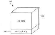
図1を参照すれば、HBMスタック105の物理的構成はロジックダイ110及びロジックダイ110の最上側にスタッキングされた複数のDRAMダイ(例えば、8個のダイ)を含む3次元DRAMすなわち“DRAMスタック115”を含む。相互連結はTSVs(through−silicon via)を通じてスタック内に形成される。HBMスタック関連技術はロジックダイ内に連結、信号調節回路を含み、その結果として、HBMの外部インターフェイスによるホストプロセッサへのDRAMチャンネルインターフェイスが実質的に変更されずに提供される。
Referring to FIG. 1, the physical configuration of the
図2を参照すれば、HBMスタック105はホストプロセッサ205(即ち、CPU又はGPU)に連結される。ホストプロセッサ205は各々が夫々のレベル1キャッシュ215を有する複数のコア210を含む。レベル2キャッシュ220はレベル1キャッシュ215に連結され、第1メモリ制御器225はインターフェイスをオフチップメーンメモリ230に提供する。第2メモリ制御器235はHBMスタック105へのインターフェイスを提供する。HBMスタック105はHBMスタック105のロジックダイ内にキャッシュ管理部CMを含む。HBMスタック105はそのキャッシュ管理部CMと共にホストプロセッサ205によってレベル3キャッシュ(又はレベル3キャッシュを有するシステムにおけるレベル4キャッシュ)として採択される。HBMインターフェイス245はJESD235Aに相応しいインターフェイスであり、即ちこれはJESD235A標準によって指定されたコンダクター(conductors)及びシグナリングプロトコル(signaling protocols)を提供する。
Referring to FIG. 2, the
図3を参照すれば、一部の実施形態において、HBMスタック105はロジックダイ110を含み、ロジックダイ110は図3においてch0乃至ch7により示したチャンネルと称される8個の内部インターフェイスを通じてDRAMスタック115内のDRAMに連結される。
Referring to FIG. 3, in some embodiments, the
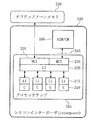
図4を参照すれば、一実施形態において、HBMスタック105は前述したようにDRAMスタック115及びロジックダイ110を含み、ロジックダイ110はキャッシュ管理部CMを具現する複数の構成要素を含む。HBMインターフェイス245による命令及びアドレスライン305はHBMスタック105のロジックダイ110内の命令変換機310及びアドレス変換機315に連結される。命令及びアドレスライン305は、例えばHBMインターフェイス245の8個のチャンネルの各々のために6個の行の命令/アドレスライン及び8個の列の命令/アドレスラインを含む。
Referring to FIG. 4, in one embodiment, the
動作において、アドレス変換機315は命令(即ち読出し命令又は書込み命令)が遂行されるための物理的メモリアドレスを周期的に受信する。その後、アドレス変換機315はアドレスをタッグ値、タッグアドレス、及びデータアドレスに変換する。タッグ値は‘‘キャッシュヒット’’が発生したか否かを決定するのに利用される(即ち、キャッシュ内のアドレスがHBMインターフェイス245を通じて受信されたアドレスに現在割当されているか否かを決定するのに利用される)。例えば、キャッシュ管理部CMはタッグアドレスにおいてタッグ値を読み出し、或いはフェッチし、それをアドレス変換機315によって生成されたタッグ値と比較する。(即ち、以下において詳細に説明するタッグ比較器320を通じて)仮に受信された物理的アドレスから形成されたタッグ値が、アドレス変換機315によってDRAMスタック115においてタッグアドレスに格納されたタッグ値と同一である場合、キャッシュヒットは発生する。即ち、キャッシュ内のアドレスはプロセッサの物理的メモリ空間において、受信されたアドレスに現在割当されている。受信された物理的アドレスから形成されたタッグ値がDRAMスタック115のタッグアドレスに格納されたタッグ値と同一でない場合(本明細書においては、その状態を‘‘キャッシュミス’’と称す)、キャッシュ内アドレスはプロセッサの物理的メモリ空間において、受信されたアドレスに現在割当されていない。
In operation, the
タッグ比較器320は比較に使用される。即ち、前記比較は受信された物理的アドレスから形成されたタッグ値とタッグアドレスに格納されたタッグ値とを比較する。タッグ比較器320の出力はキャッシュヒット信号と称される信号であり、キャッシュヒット信号はキャッシュヒットが発生する場合、真値(即ち、二進‘‘1’’値)及びキャッシュミスが発生する場合、偽値(即ち二進‘‘0’’値)を有する。
A
命令変換機310はHBMインターフェイス245を通じて受信された命令に応答して命令を生成しDRAMスタック115において命令が実行される。例えば、HBMインターフェイス245を通じて受信された命令が読出し命令であれば、命令変換機310は命令を生成してデータアドレスに格納されたデータワードを読み出し、命令を生成してタッグアドレスに格納されたタッグ値を読み出す。前記命令の各々は複数のマイクロ動作を含み、或いは構成される、即ち読出し命令は読出し動作に後続する活性動作を含む。
The
HBMインターフェイス245を通じて受信された命令が書込み命令である場合、命令変換機310は先ず命令を生成させてタッグアドレスに格納されたタッグを読み出し、タッグ値がアドレス変換機315によって生成されたタッグ値と同一である場合、書込み命令を生成させて、DRAMスタック115にデータ書込み動作をする。上記したように、ホストプロセッサ205がキャッシュ管理部CMの具現を不必要とし、さらにロジックダイ110内にキャッシュ管理部CMを含むことは第2番目の命令(書込み命令)がホストプロセッサ205ではない、むしろロジックダイ110において生成されることによって、効率性を改善できる。
If the command received through the
タッグ値及びデータをフェッチすることは並列的又は直列的に遂行される。例えば、キャッシュ管理部CMが並列モードにより動作する場合、タッグ値及びデータは並列的にフェッチされ、フェッチされたタッグ値はアドレス変換機315によって生成されたタッグ値とタッグ比較器320によって比較され、そして前記2つのタッグ値とが同一である場合、HBMインターフェイス245を通じてデータ読出しデータは返還される。そうでない場合にはキャッシュミスは以下に後述するようにHBMインターフェイス245を通じてホストプロセッサ205に伝達される。キャッシュ管理部CMが直列モードにより動作する場合、タッグ値が先ずフェッチされ、フェッチされたタッグ値はアドレス変換機315によって生成されたタッグ値とタッグ比較器320によって比較され、そして2つのタッグ値が同一である場合、データはフェッチされ、HBMインターフェイス245を通じて返還される。同一でなければ、キャッシュミスはHBMインターフェイス245を通じてホストプロセッサ205に伝達される。直列モードによる動作は並列モードによる動作よりさらに電力的に効率的である。なぜならば、直列モードにおいてデータフェッチ動作はただキャッシュヒットの場合のみに遂行されるためである。並列モードによる動作は直列モードによる動作より速い。なぜならば、並列モードにおいてはタッグ値フェッチ及びデータフェッチは同時に遂行される。キャッシュ管理部CMはモード選択器(即ち、制御レジスターのビット)を含み、モード選択器はキャッシュ管理部CMが並列モードにより動作するか、或いは直列モードにより動作するかを制御する。モード選択器はHBMインターフェイス245を通じて、ホストプロセッサ205によって、即ち、新しい値を制御レジスターに書き込む命令によって制御される。
Fetching tag values and data can be performed in parallel or serially. For example, when the cache management unit CM operates in the parallel mode, the tag value and data are fetched in parallel, and the fetched tag value is compared with the tag value generated by the
キャッシュ管理部CMは各々のタッグと共に、2ビットのメタデータを格納する。前記2ビットは
(i)対応するデータワードが有効であるか、或いは無効であるかを指示するビット(‘‘有効ビット’’)、
(ii)対応するデータワードがクリーン(clean)又はダーティ(dirty)であるかを指示するビット(‘‘ダーティビット’’)
である。補助記憶ストレージ内の対応するデータがアップデートされること(言葉を変えれば、クリーン(clean))無しにキャッシュ内のデータがアップデートされる場合に、キャッシュ内データはダーティとして看做され、そしてキャッシュに対応するデータがアップデートされること(言葉を変えれば有効な)無しに補助記憶ストレージ内のデータがアップデートされる場合、キャッシュ内のデータは無効であると看做される。
The cache management unit CM stores 2-bit metadata together with each tag. The two bits are (i) a bit (“valid bit”) indicating whether the corresponding data word is valid or invalid,
(Ii) a bit ("dirty bit") indicating whether the corresponding data word is clean or dirty
It is. If the data in the cache is updated without the corresponding data in the auxiliary storage being updated (in other words, clean), the data in the cache is considered dirty, and If the data in the auxiliary storage is updated without the corresponding data being updated (valid in other words), the data in the cache is considered invalid.
さらに、HBMインターフェイス245を通じて受信された命令は前述したように、キャッシュヒット信号の真値又は偽値(キャッシュヒット又はキャッシュミスに各々対応する)の結果をもたらす。HBMインターフェイス245を通じてHBMスタック105によって受信された任意の命令が完了する場合、キャッシュ管理部CMは3つの値を生成させる。1つはキャッシュヒット信号であり、1つはダーティビットであり、1つは有効ビットである。前記値は他の機能のために使用されないHBMインターフェイス245の1つ以上のピンを使用してHBMインターフェイス245を通じてホストプロセッサ205に伝達される。前記ピンは
(i)8個のチャンネルの各々の212個のピンの中の任意のピンではなく、また
(ii)RESET、TEMP[2:0]、又はCATTRIPピンの中の任意のピンではない。後に使用されるために予約されたピン(RFUピン)として、JESD235A標準によって定義されたピンが使用される。例えば、一実施形態において、RFUピンは命令が実行された後、データバースト(data burst)の第1データサイクルの間にキャッシュヒット信号を伝送するのに使用され、データバーストの次のデータサイクルの間にダーティビットの値を伝送するために使用される。キャッシュヒット信号及びダーティビットの伝送はデータバーストのデータの伝送に同期化される。一部の実施形態において、複数のRFUピンはキャッシュヒット信号、ダーティビット、及び/又は有効ビットを伝送するために使用される。
Further, instructions received through the
キャッシュ内においてデータを無効化するために、ホストプロセッサ205は“無効化”信号を無効化されるデータのアドレスと共にHBMインターフェイス245を通じてロジックダイ110に伝送する。無効化信号はキャッシュヒット信号をホストプロセッサ205に伝送するために使用されるHBMインターフェイス245の同一のピン(即ち、RFUピン)を通じて伝送される。アドレスはHBMインターフェイス245のCAバスを通じて伝送される。そして、前記情報を通じて、ロジックダイ110はDRAMスタック115に格納された対応する有効ビットをアップデートする。
To invalidate the data in the cache, the
一部の実施形態において、RFUピンはまたキャッシュ一貫性(coherency)を維持するために使用される。即ち、図2に示したようなマルチコアシステムにおいて補助記憶ストレージ(即ち、オフチップメーンメモリ230)とキャッシュとの間における一貫性を維持させる。前記マルチコアシステムにおいて、レベル3キャッシュ(HBMスタック105にて具現される)及び補助記憶ストレージはコア210の各々によって読み出されるか、或は修正される。
In some embodiments, the RFU pin is also used to maintain cache coherency. That is, consistency is maintained between the auxiliary storage (ie, the off-chip main memory 230) and the cache in the multi-core system as shown in FIG. In the multi-core system, the level 3 cache (implemented in the HBM stack 105) and auxiliary storage are read or modified by each of the
ロジックダイ110のスケジューラー325は命令変換機310及びアドレス変換機315の各々から命令及びアドレスを受信し、DRAMスタック115上における前記命令の実行を予定する。ロジックダイ110のデータバッファ330はデータがHBMインターフェイス245を通じて受信された後及び/又はデータがDRAMスタック115から読み出された後に一時的にデータを格納するために使用される。スケジューラー325及びデータバッファ330は所定の比率の変化の収容を助ける。
The
前記変化は次の通りである。
(i)HBMインターフェイス245を通じて命令が受信され、
(ii)DRAMスタック115上において命令が実行され、
(iii)HBMインターフェイス245を通じてデータが伝送されるか、或いは受信され、
(iv)DRAMスタック115からデータが読み出されるか、或はDRAMスタック115にデータが書き込まれる。
The changes are as follows.
(I) a command is received through the
(Ii) an instruction is executed on the
(Iii) data is transmitted or received through the
(Iv) Data is read from the
JESD235A標準は擬似(pseudo)チャンネルモードにより動作を提供し、前記擬似チャンネルモードにより、8個の128ビットチャンネルの各々は2つの半独立的な(semi−independent)擬似チャンネルとして動作する。このようなモードにおいては、2つの擬似チャンネルが個別的に命令をデコーディングし、実行するにも拘らず、擬似チャンネルの各々の対はチャンネルの行及び列命令バスを共有するだけでなく、CK及びCKE入力も共有する。一部の実施形態において、前記モードはタッグ値を格納するのに使用される。チャンネルの全体128ビット幅データバス(DQバス)がDRAMスタック115からタッグ値を読み出すか、或いはタッグ値を使うために使用される場合、各々のタッグ値は非常に効率的ではない(即ち、25%程度の効率)結果をもたらす32ビットワードである。擬似チャンネルモードにおいて前記バスの幅の単なる半分(即ち64ビット)のみがタッグ値を読み出すか、或いは使うのに使用される場合、さらに高い効率(即ち、50%程度)をもたらす。
The JESD235A standard provides operation in pseudo channel mode, where each of the eight 128-bit channels operates as two semi-independent pseudo channels. In such a mode, despite the two pseudo channels individually decoding and executing instructions, each pair of pseudo channels not only shares the channel row and column instruction buses, but also CK. And CKE inputs are also shared. In some embodiments, the mode is used to store tag values. If a channel's entire 128-bit wide data bus (DQ bus) is used to read or use tag values from
DRAMのバンクの各々は16個のサブアレイを含むか、又は構成する。図5を参照すれば、一部の実施形態において、各々のデータワードは64バイト(512ビット)の長さであり、各々のタッグ値は4バイト(32ビット)の長さである。即ち、長さの比率は16:1である。タッグ値及びデータは互いに異なるチャンネルを通じてアクセスされる。例えば、データはチャンネル1乃至15を通じてアクセスされ、タッグ値はチャンネル0を通じてアクセスされる。前記実施形態において、並列的なデータのアクセスが可能であるが、タッグアクセスは図示した点線楕円により示したように、バンク衝突(bank conflicts)を経験する。したがって、図6を参照すれば、一実施形態において、タッグは互いに異なるサブアレイに格納され、前記サブアレイは本明細書においてSALP(subarray level parallelism)と称する方法を使用して並列にアクセスされる。前記実施形態において、タッグアクセスが同時に処理されることが可能であり、これを通じてタッグアクセスが同一のバンクに行われる場合にも、タッグアクセスのための衝突を避けることができる。 Each bank of DRAMs includes or constitutes 16 subarrays. Referring to FIG. 5, in some embodiments, each data word is 64 bytes (512 bits) long and each tag value is 4 bytes (32 bits) long. That is, the length ratio is 16: 1. Tag values and data are accessed through different channels. For example, data is accessed through channels 1 through 15 and tag values are accessed through channel 0. In the above embodiment, parallel data access is possible, but tag access experiences bank conflicts, as shown by the dotted ellipses shown. Therefore, referring to FIG. 6, in one embodiment, the tags are stored in different subarrays, which are accessed in parallel using a method referred to herein as SALP (subarray level parallelism). In the above embodiment, tag accesses can be processed at the same time, and even when tag accesses are made to the same bank, the collision for tag access can be avoided.
前述した観点において、ロジックダイ110内にキャッシュ管理部CMを含むHBMスタック105はキャッシュ管理部CMがないHBMスタック関連技術に対比して多くの長所を有する。キャッシュ管理部CMを含むHBMスタック105の使用はホストプロセッサのサイズ、価額、及び電力消費を減少させながら、ホストプロセッサ205内にキャッシュ管理部CMを含む必要がないようにし、同一のリソースをホストプロセッサ205において他の用途として使用できるようにする。その上に、条件付実行はこのような条件付実行がホストプロセッサ205を伴う場合よりHBMスタック105内において全的に遂行される場合さらに速い。例えば、書込み命令はキャッシュヒット決定がホストプロセッサ205のキャッシュ管理部CM内において行われる場合より、HBMスタック105内において行われるキャッシュヒットの場合にさらに速やかに実行できる。
In view of the above, the
‘‘第1’’、‘‘第2’’、‘‘第3’’等の用語は本明細書において、多様な要素、構成要素、領域、層、及び/又は部分を説明するために使用したが、前記要素、構成要素、領域、層、及び/又は部分は前記用語に限定されない。前記用語は1つの要素、構成要素、領域、層、又は部分をその他の要素、構成要素、領域、層、又は部分と単に区分するために使用した。したがって、第1要素、構成要素、領域、層、又は部分は発明の概念の思想及び範囲を逸脱せずに、第2要素、構成要素、領域、層、又は部分に指定できる。 Terms such as “first”, “second”, “third”, etc. are used herein to describe various elements, components, regions, layers, and / or portions. However, the elements, components, regions, layers, and / or portions are not limited to the above terms. The terms are used merely to distinguish one element, component, region, layer or part from another element, component, region, layer or part. Accordingly, a first element, component, region, layer, or part can be designated as a second element, component, region, layer, or part without departing from the spirit and scope of the inventive concept.
‘‘下’’及び‘‘上’’等の空間的に関連された用語は1つの要素及び特徴と1つの図面に説明したその他の要素又は特徴との関係の説明を容易にするために本明細書において使用した。前記空間的に関連された用語は図面において説明する方向に追加して、使用される装置及び動作の互いに異なる方向を含む。例えば、図面において装置が裏返した場合には他の要素又は特徴の‘‘下’’のような用語として説明する要素は他の要素又は特徴の‘‘上’’に配置される。したがって、例示的な用語‘‘下’’は下と上を全て含む。装置は他の方向に配置される。例えば、90°又は他の方向に回転される。本明細書において使用される空間的に関連された用語はこれにしたがって解釈されなければならない。また、1つの層が2つの層間にあることを言及する場合、2つの層間に唯一の層であるか、或いは1つ以上の介在した層が存在できることは明らかである。 Spatially related terms such as `` lower '' and `` upper '' are used to facilitate the description of the relationship between one element and feature and the other elements or features described in one drawing. Used in the specification. The spatially related terms include different directions of device and operation used in addition to the directions described in the drawings. For example, when the apparatus is turned upside down in the drawing, an element described as a term such as “under” of another element or feature is placed “above” of the other element or feature. Thus, the exemplary term 'lower' includes all lower and upper. The device is placed in the other direction. For example, it is rotated 90 ° or other directions. The spatially related terms used herein should be interpreted accordingly. Also, when mentioning that one layer is between two layers, it is clear that there can be only one layer between two layers, or there can be one or more intervening layers.
本明細書において使用した用語は特定実施形態のみを説明するためのものであり、本発明の概念を制限しない。本明細書において使用した用語‘‘実質的に’’、‘‘約’’及びこれと類似な用語は近似の用語として使用し、学術的な用語として使用されず、これらによって認識される測定又は計算値は固有の偏差を説明するためであり、これは当業者に自明である。本明細書において使用したように‘‘主要成分’’という用語は組成物の少なくとも半分を構成する成分を意味し、‘‘主要部分’’は複数の項目に適用される時、項目の少なくとも半分を意味する。 The terminology used herein is for the purpose of describing particular embodiments only and does not limit the concept of the invention. The terms `` substantially '', `` about '' and similar terms used herein are used as approximate terms and are not used as academic terms, but are recognized by The calculated value is to explain the inherent deviation, which is obvious to those skilled in the art. As used herein, the term `` major component '' means a component that constitutes at least half of the composition, and `` major portion '' when applied to multiple items is at least half of the items. Means.
本明細書において使用した単数形態は文脈上、特に明示されていない限り、複数形態を含む。本明細書において使用する‘‘含む’’という用語は明示された特徴、整数、段階、動作、構成要素、及び/又は構成要素の存在を示すが、存在を排除しないと解釈することが自明である。又は1つ以上の他の特徴、整数、段階、動作、要素、構成要素、及び/又はグループの追加を含む。本明細書において使用したように‘‘及び/又は’’という用語は1つ以上の関連されて列挙された項目の任意及びすべての組合を含む。‘‘少なくとも1つ’’のような表現は要素目録の前にある場合に要素の全体目録を修正し、目録の個別要素を修正しない。また、本発明の概念の実施形態を記述する時、‘‘することができる’’を使用することは‘‘本発明の1つ以上の実施形態’’を意味する。また‘‘例示的な’’という用語は例又は説明を意味する。本明細書において使用されたように用語‘‘使用’’、‘‘使用する’’及び‘‘使用された’’は各々‘‘利用’’、‘‘利用する”及び‘‘利用された”と同意語と看做される。 As used herein, the singular forms include the plural unless the context clearly indicates otherwise. As used herein, the term “comprising” is intended to indicate the presence of an explicit feature, integer, step, action, component, and / or component, but is to be interpreted as not excluding the presence. is there. Or including the addition of one or more other features, integers, steps, actions, elements, components, and / or groups. As used herein, the term 'and / or' includes any and all combinations of one or more of the associated listed items. An expression such as 'at least one' modifies the element's entire inventory when it precedes the element inventory and does not modify the individual elements of the inventory. Also, when describing embodiments of the inventive concept, the use of “can do” means “one or more embodiments of the invention”. Also, the term “exemplary” means an example or description. As used herein, the terms `` use '', `` use '' and `` used '' are `` used '', `` used '' and `` used '' respectively. Is regarded as a synonym.
要素又は層がその他の要素又は層の‘‘上”にあること、‘‘連結された”、‘‘結合された”又は隣接すると言及する場合、1つ以上の介在要素又は層が存在できる。対照的に1つの要素又は層が他の要素又は層に‘‘直接的に”、‘‘直接的に連結された”、‘‘直接的に結合された”又は‘‘直ちに隣接する”と言及する時、介在する要素又は層が存在しない。 Where an element or layer is referred to as being “on”, “connected”, “coupled” or adjacent to another element or layer, there can be one or more intervening elements or layers. In contrast, one element or layer is referred to as “directly”, “directly connected”, “directly coupled” or “immediately adjacent” to another element or layer. There are no intervening elements or layers.
本明細書において列挙した任意の数値範囲は列挙した範囲内に含まれた同一の数値精度のすべての下位範囲を含むように意図される。例えば、1.0乃至10.0の範囲には指定された1.0の値と10.0の値の間のすべての部分範囲が含まれる(最小の値が1.0以上)。例えば、2.4乃至7.6のような値があり得る。本明細書に引用された最大数値制限はここに含まれるすべての低い数値制限を含むように意図され、本明細書に引用された任意の最小数値制限はここに含まれるすべてのさらに高い数値制限を含むように意図される。 Any numerical range recited herein is intended to include all sub-ranges with the same numerical accuracy contained within the recited range. For example, the range of 1.0 to 10.0 includes all subranges between the specified value of 1.0 and 10.0 (the minimum value is 1.0 or greater). For example, there may be values such as 2.4 to 7.6. The maximum numerical limits cited herein are intended to include all lower numerical limits included herein, and any minimum numerical limits cited herein shall be construed to include all higher numerical limits included herein. Is intended to include
メモリ内キャッシュ管理部が有する高帯域幅メモリの例示的な実施形態を本明細書に具体的に説明し例示したが、多くの変形及び変更が当業者に自明である。したがって、本発明の原理にしたがって構成されたメモリ内キャッシュ管理部を有する高帯域幅メモリは本明細書に具体的に説明した以外により具現できる。本発明はまた次の特許請求の範囲及びその均等物により定義される。 While exemplary embodiments of the high bandwidth memory included in the in-memory cache manager are specifically described and illustrated herein, many variations and modifications will be apparent to those skilled in the art. Accordingly, a high bandwidth memory having an in-memory cache manager configured according to the principles of the present invention can be implemented other than as specifically described herein. The invention is also defined by the following claims and their equivalents.
105 HBMスタック
110 ロジックダイ
115 DRAMスタック
205 ホストプロセッサ
210 コア
215 レベル1キャッシュ
220 レベル2キャッシュ
225 第1メモリ制御器
230 オフチップメーンメモリ
235 第2メモリ制御器
240 シリコンインターポーザ
245 HBMインターフェイス
305 アドレスライン
310 命令変換機
315 アドレス変換機
320 タッグ比較器
325 スケジューラー
330 データバッファ
105
Claims (20)
複数のメモリダイを含むメモリスタックと、
ロジックダイと、を含み、
前記メモリダイは、前記ロジックダイ上にスタッキングされ、前記ロジックダイに連結され、
前記ロジックダイは、前記メモリシステムに対する外部インターフェイスを含み、
前記ロジックダイは、キャッシュ管理部を含むことを特徴とするメモリシステム。 In the memory system,
A memory stack including a plurality of memory dies;
A logic die, and
The memory die is stacked on the logic die and coupled to the logic die;
The logic die includes an external interface to the memory system;
The memory system, wherein the logic die includes a cache management unit.
前記キャッシュヒット信号は、前記第1タッグ値が前記第1命令の実行の結果値と同一である場合、真値を有し、前記第1タッグ値が前記第1命令の実行の結果値と同一でない場合、偽値を有することを特徴とする請求項3に記載のメモリシステム。 The cache management unit includes a tag comparator that generates a cache hit signal;
The cache hit signal has a true value when the first tag value is the same as a result value of execution of the first instruction, and the first tag value is the same as a result value of execution of the first instruction. 4. The memory system of claim 3, wherein the memory system has a false value if not.
前記ホストプロセッサに連結された第1メモリシステムと、
前記ホストプロセッサに連結された第2メモリシステムと、を含み、
前記第1メモリシステムは、
複数のメモリダイを含むメモリスタックと、
ロジックダイと、を含み、
前記メモリダイは、前記ロジックダイ上にスタッキングされ、前記ロジックダイに連結され、
前記ロジックダイは、メモリシステムに対する外部インターフェイスを具備し、前記ロジックダイは、キャッシュ管理部を含み、
前記第2メモリシステムは、前記第1メモリシステムに対する補助記憶装置として動作することを特徴とするプロセシングシステム。 A host processor;
A first memory system coupled to the host processor;
A second memory system coupled to the host processor;
The first memory system includes:
A memory stack including a plurality of memory dies;
A logic die, and
The memory die is stacked on the logic die and coupled to the logic die;
The logic die includes an external interface to a memory system, the logic die includes a cache management unit;
The processing system, wherein the second memory system operates as an auxiliary storage device for the first memory system.
前記キャッシュヒット信号は、前記第1タッグ値が前記第1命令の実行の結果値と同一である場合に真値、及び前記第1タッグ値が前記第1命令の実行の結果値と同一でない場合、偽値を有することを特徴とする請求項15に記載のプロセシングシステム。 The cache management unit includes a tag comparator that generates a cache hit signal;
The cache hit signal is a true value when the first tag value is the same as a result value of the execution of the first instruction, and when the first tag value is not the same as a result value of the execution of the first instruction. 16. The processing system of claim 15, wherein the processing system has a false value.
前記方法は、
前記ロジックダイによって前記外部インターフェイスを通じて受信されたアドレスを変換して、第1タッグ値、前記メモリスタックのデータアドレス、及び前記メモリスタックのタッグアドレスを生成する段階を含むことを特徴とするメモリスタックを動作させる方法。 A method of operating a memory stack including a plurality of memory dies and logic dies, wherein the memory dies are stacked on and coupled to the logic dies, the logic dies comprising an external interface to a memory system;
The method
Transforming an address received through the external interface by the logic die to generate a first tag value, a data address of the memory stack, and a tag address of the memory stack. How to make it work.
前記キャッシュヒット信号は、前記第1タッグ値が前記第1命令の実行の結果値と同一である場合に真値、及び前記第1タッグ値が前記第1命令の実行の結果値と同一でない場合、偽値を有することを特徴とする請求項19に記載のメモリスタックを動作させる方法。 Generating a cache hit signal by the logic die;
The cache hit signal is a true value when the first tag value is the same as a result value of the execution of the first instruction, and when the first tag value is not the same as a result value of the execution of the first instruction. 20. The method of operating a memory stack of claim 19, wherein the method has a false value.
Applications Claiming Priority (4)
| Application Number | Priority Date | Filing Date | Title |
|---|---|---|---|
| US201662367062P | 2016-07-26 | 2016-07-26 | |
| US62/367062 | 2016-07-26 | ||
| US15/272,339 US10180906B2 (en) | 2016-07-26 | 2016-09-21 | HBM with in-memory cache manager |
| US15/272339 | 2016-09-21 |
Publications (2)
| Publication Number | Publication Date |
|---|---|
| JP2018018513A true JP2018018513A (en) | 2018-02-01 |
| JP2018018513A5 JP2018018513A5 (en) | 2020-06-18 |
Family
ID=61010011
Family Applications (1)
| Application Number | Title | Priority Date | Filing Date |
|---|---|---|---|
| JP2017110782A Pending JP2018018513A (en) | 2016-07-26 | 2017-06-05 | Memory system, processing system, and method for operating memory stacks |
Country Status (5)
| Country | Link |
|---|---|
| US (1) | US10180906B2 (en) |
| JP (1) | JP2018018513A (en) |
| KR (1) | KR102404643B1 (en) |
| CN (1) | CN107656878B (en) |
| TW (1) | TWI703440B (en) |
Families Citing this family (16)
| Publication number | Priority date | Publication date | Assignee | Title |
|---|---|---|---|---|
| US10936221B2 (en) | 2017-10-24 | 2021-03-02 | Micron Technology, Inc. | Reconfigurable memory architectures |
| US11281608B2 (en) * | 2017-12-11 | 2022-03-22 | Micron Technology, Inc. | Translation system for finer grain memory architectures |
| KR102505913B1 (en) * | 2018-04-04 | 2023-03-07 | 삼성전자주식회사 | Memory module and memory system including memory module) |
| CN111971660A (en) * | 2018-06-05 | 2020-11-20 | 拉姆伯斯公司 | High speed buffer dynamic random access memory |
| KR102605205B1 (en) * | 2018-07-25 | 2023-11-24 | 에스케이하이닉스 주식회사 | Memory device and processing system |
| CN110928810B (en) * | 2018-09-20 | 2023-11-14 | 三星电子株式会社 | Outward expansion high bandwidth storage system |
| US11138135B2 (en) | 2018-09-20 | 2021-10-05 | Samsung Electronics Co., Ltd. | Scale-out high bandwidth memory system |
| KR102693213B1 (en) * | 2018-11-30 | 2024-08-09 | 에스케이하이닉스 주식회사 | Memory system |
| CN111679785A (en) | 2019-03-11 | 2020-09-18 | 三星电子株式会社 | Memory device for processing operation, operating method thereof and data processing system |
| DE102020105628A1 (en) | 2019-03-11 | 2020-09-17 | Samsung Electronics Co., Ltd. | Method for performing internal processing operations with a predefined protocol interface of a storage device |
| US11436165B2 (en) * | 2019-05-01 | 2022-09-06 | Samsung Electronics Co., Ltd. | High bandwidth memory system |
| US10915451B2 (en) * | 2019-05-10 | 2021-02-09 | Samsung Electronics Co., Ltd. | Bandwidth boosted stacked memory |
| US11216385B2 (en) * | 2019-05-15 | 2022-01-04 | Samsung Electronics Co., Ltd. | Application processor, system-on chip and method of operating memory management unit |
| US11226816B2 (en) * | 2020-02-12 | 2022-01-18 | Samsung Electronics Co., Ltd. | Systems and methods for data placement for in-memory-compute |
| KR20220127601A (en) * | 2021-03-11 | 2022-09-20 | 삼성전자주식회사 | Memory system, memory device of performing internal processing operations with interface, operation method of the memory device having the same |
| US11901035B2 (en) | 2021-07-09 | 2024-02-13 | Taiwan Semiconductor Manufacturing Company, Ltd. | Method of differentiated thermal throttling of memory and system therefor |
Citations (7)
| Publication number | Priority date | Publication date | Assignee | Title |
|---|---|---|---|---|
| JPH08221324A (en) * | 1995-01-17 | 1996-08-30 | Advanced Risc Mach Ltd | Access to cache memory |
| JPH11212868A (en) * | 1998-01-28 | 1999-08-06 | Oki Electric Ind Co Ltd | Snoop cash memory control system |
| US20120173809A1 (en) * | 2011-01-05 | 2012-07-05 | Tae-Kyeong Ko | Memory Device Having DRAM Cache and System Including the Memory Device |
| US20120314513A1 (en) * | 2011-06-09 | 2012-12-13 | Semiconductor Energy Laboratory Co., Ltd. | Semiconductor memory device and method of driving semiconductor memory device |
| US20130138892A1 (en) * | 2011-11-30 | 2013-05-30 | Gabriel H. Loh | Dram cache with tags and data jointly stored in physical rows |
| US20140181417A1 (en) * | 2012-12-23 | 2014-06-26 | Advanced Micro Devices, Inc. | Cache coherency using die-stacked memory device with logic die |
| US20150016172A1 (en) * | 2013-07-15 | 2015-01-15 | Advanced Micro Devices, Inc. | Query operations for stacked-die memory device |
Family Cites Families (11)
| Publication number | Priority date | Publication date | Assignee | Title |
|---|---|---|---|---|
| WO1996012229A1 (en) * | 1994-10-14 | 1996-04-25 | Silicon Graphics, Inc. | Indexing and multiplexing of interleaved cache memory arrays |
| US8341352B2 (en) * | 2007-04-17 | 2012-12-25 | International Business Machines Corporation | Checkpointed tag prefetcher |
| KR101728067B1 (en) * | 2010-09-03 | 2017-04-18 | 삼성전자 주식회사 | Semiconductor memory device |
| US20120221785A1 (en) * | 2011-02-28 | 2012-08-30 | Jaewoong Chung | Polymorphic Stacked DRAM Memory Architecture |
| US20120297256A1 (en) | 2011-05-20 | 2012-11-22 | Qualcomm Incorporated | Large Ram Cache |
| US9189399B2 (en) * | 2012-11-21 | 2015-11-17 | Advanced Micro Devices, Inc. | Stack cache management and coherence techniques |
| US9053039B2 (en) | 2012-12-21 | 2015-06-09 | Advanced Micro Devices, Inc. | Installation cache |
| US9477605B2 (en) | 2013-07-11 | 2016-10-25 | Advanced Micro Devices, Inc. | Memory hierarchy using row-based compression |
| CN104575584B (en) | 2013-10-23 | 2018-11-30 | 钰创科技股份有限公司 | System-in-package memory module with embedded memory |
| KR20150062646A (en) * | 2013-11-29 | 2015-06-08 | 삼성전자주식회사 | Electronic System and Operating Method of the same |
| US10078597B2 (en) * | 2015-04-03 | 2018-09-18 | Via Alliance Semiconductor Co., Ltd. | System and method of distinguishing system management mode entries in a translation address cache of a processor |
-
2016
- 2016-09-21 US US15/272,339 patent/US10180906B2/en active Active
-
2017
- 2017-01-31 KR KR1020170013952A patent/KR102404643B1/en active IP Right Grant
- 2017-06-05 TW TW106118496A patent/TWI703440B/en active
- 2017-06-05 JP JP2017110782A patent/JP2018018513A/en active Pending
- 2017-06-29 CN CN201710515631.0A patent/CN107656878B/en active Active
Patent Citations (11)
| Publication number | Priority date | Publication date | Assignee | Title |
|---|---|---|---|---|
| JPH08221324A (en) * | 1995-01-17 | 1996-08-30 | Advanced Risc Mach Ltd | Access to cache memory |
| US5717892A (en) * | 1995-01-17 | 1998-02-10 | Advanced Risc Machines Limited | Selectively operable cache memory |
| JPH11212868A (en) * | 1998-01-28 | 1999-08-06 | Oki Electric Ind Co Ltd | Snoop cash memory control system |
| US20120173809A1 (en) * | 2011-01-05 | 2012-07-05 | Tae-Kyeong Ko | Memory Device Having DRAM Cache and System Including the Memory Device |
| US20120314513A1 (en) * | 2011-06-09 | 2012-12-13 | Semiconductor Energy Laboratory Co., Ltd. | Semiconductor memory device and method of driving semiconductor memory device |
| KR20120137282A (en) * | 2011-06-09 | 2012-12-20 | 가부시키가이샤 한도오따이 에네루기 켄큐쇼 | Semiconductor memory device and method of driving semiconductor memory device |
| JP2013016244A (en) * | 2011-06-09 | 2013-01-24 | Semiconductor Energy Lab Co Ltd | Semiconductor storage device and method for driving semiconductor storage device |
| US20130138892A1 (en) * | 2011-11-30 | 2013-05-30 | Gabriel H. Loh | Dram cache with tags and data jointly stored in physical rows |
| JP2015503160A (en) * | 2011-11-30 | 2015-01-29 | アドバンスト・マイクロ・ディバイシズ・インコーポレイテッドAdvanced Micro Devices Incorporated | DRAM cache with tags and data stored together in physical rows |
| US20140181417A1 (en) * | 2012-12-23 | 2014-06-26 | Advanced Micro Devices, Inc. | Cache coherency using die-stacked memory device with logic die |
| US20150016172A1 (en) * | 2013-07-15 | 2015-01-15 | Advanced Micro Devices, Inc. | Query operations for stacked-die memory device |
Non-Patent Citations (1)
| Title |
|---|
| JEDEC STANDARD HIGH BANDWIDTH MEMORY (HBM) DRAM, JESD235A, JPN7020003277, November 2015 (2015-11-01), US, pages 1 - 20, ISSN: 0004367279 * |
Also Published As
| Publication number | Publication date |
|---|---|
| US20180032437A1 (en) | 2018-02-01 |
| KR20180012180A (en) | 2018-02-05 |
| US10180906B2 (en) | 2019-01-15 |
| KR102404643B1 (en) | 2022-06-02 |
| TWI703440B (en) | 2020-09-01 |
| CN107656878B (en) | 2023-06-13 |
| TW201804328A (en) | 2018-02-01 |
| CN107656878A (en) | 2018-02-02 |
Similar Documents
| Publication | Publication Date | Title |
|---|---|---|
| JP2018018513A (en) | Memory system, processing system, and method for operating memory stacks | |
| CN111279322B (en) | Processing system and method for mixed writing in 3D stack memory | |
| US10579462B2 (en) | Method and apparatus for using an error signal to indicate a write request error and write request acceptance | |
| US20180039424A1 (en) | Method for accessing extended memory, device, and system | |
| JP2000242559A (en) | Information processor and semiconductor device | |
| JP6710219B2 (en) | DRAM circuit with integrated processor | |
| JP2021507414A (en) | Scheduling memory requests for interlocking memory devices | |
| EP4060505A1 (en) | Techniques for near data acceleration for a multi-core architecture | |
| US20130191587A1 (en) | Memory control device, control method, and information processing apparatus | |
| JP6370958B2 (en) | device | |
| US11194744B2 (en) | In-line memory module (IMM) computing node with an embedded processor(s) to support local processing of memory-based operations for lower latency and reduced power consumption | |
| US20120254530A1 (en) | Microprocessor and memory access method | |
| KR20120132871A (en) | Processor and method for Processing Data the same, and Memory system having the same | |
| JP2009181221A (en) | Memory control method | |
| JP2002074942A (en) | Semiconductor memory | |
| JP2009157576A (en) | Memory control circuit and memory control method |
Legal Events
| Date | Code | Title | Description |
|---|---|---|---|
| A521 | Request for written amendment filed |
Free format text: JAPANESE INTERMEDIATE CODE: A523 Effective date: 20200511 |
|
| A621 | Written request for application examination |
Free format text: JAPANESE INTERMEDIATE CODE: A621 Effective date: 20200511 |
|
| A871 | Explanation of circumstances concerning accelerated examination |
Free format text: JAPANESE INTERMEDIATE CODE: A871 Effective date: 20200511 |
|
| A975 | Report on accelerated examination |
Free format text: JAPANESE INTERMEDIATE CODE: A971005 Effective date: 20200519 |
|
| A977 | Report on retrieval |
Free format text: JAPANESE INTERMEDIATE CODE: A971007 Effective date: 20200917 |
|
| A131 | Notification of reasons for refusal |
Free format text: JAPANESE INTERMEDIATE CODE: A131 Effective date: 20201020 |
|
| A02 | Decision of refusal |
Free format text: JAPANESE INTERMEDIATE CODE: A02 Effective date: 20210601 |