JP2017536070A - Method and apparatus for wireless power multi-coil mutual induction erasure - Google Patents
Method and apparatus for wireless power multi-coil mutual induction erasure Download PDFInfo
- Publication number
- JP2017536070A JP2017536070A JP2017519488A JP2017519488A JP2017536070A JP 2017536070 A JP2017536070 A JP 2017536070A JP 2017519488 A JP2017519488 A JP 2017519488A JP 2017519488 A JP2017519488 A JP 2017519488A JP 2017536070 A JP2017536070 A JP 2017536070A
- Authority
- JP
- Japan
- Prior art keywords
- power transmission
- power
- driver
- coils
- coil
- Prior art date
- Legal status (The legal status is an assumption and is not a legal conclusion. Google has not performed a legal analysis and makes no representation as to the accuracy of the status listed.)
- Granted
Links
Images
Classifications
-
- H—ELECTRICITY
- H02—GENERATION; CONVERSION OR DISTRIBUTION OF ELECTRIC POWER
- H02J—ELECTRIC POWER NETWORKS; CIRCUIT ARRANGEMENTS OR SYSTEMS FOR SUPPLYING OR DISTRIBUTING ELECTRIC POWER; SYSTEMS FOR STORING ELECTRIC ENERGY
- H02J50/00—Circuit arrangements or systems for wireless supply or distribution of electric power
- H02J50/005—Mechanical details of housing or structure aiming to accommodate the power transfer means, e.g. mechanical integration of coils, antennas or transducers into emitting or receiving devices
-
- H—ELECTRICITY
- H01—ELECTRIC ELEMENTS
- H01F—MAGNETS; INDUCTANCES; TRANSFORMERS; SELECTION OF MATERIALS FOR THEIR MAGNETIC PROPERTIES
- H01F38/00—Adaptations of transformers or inductances for specific applications or functions
- H01F38/14—Inductive couplings
-
- H—ELECTRICITY
- H02—GENERATION; CONVERSION OR DISTRIBUTION OF ELECTRIC POWER
- H02J—ELECTRIC POWER NETWORKS; CIRCUIT ARRANGEMENTS OR SYSTEMS FOR SUPPLYING OR DISTRIBUTING ELECTRIC POWER; SYSTEMS FOR STORING ELECTRIC ENERGY
- H02J50/00—Circuit arrangements or systems for wireless supply or distribution of electric power
- H02J50/10—Circuit arrangements or systems for wireless supply or distribution of electric power using inductive coupling
- H02J50/12—Circuit arrangements or systems for wireless supply or distribution of electric power using inductive coupling of the resonant type
-
- H—ELECTRICITY
- H02—GENERATION; CONVERSION OR DISTRIBUTION OF ELECTRIC POWER
- H02J—ELECTRIC POWER NETWORKS; CIRCUIT ARRANGEMENTS OR SYSTEMS FOR SUPPLYING OR DISTRIBUTING ELECTRIC POWER; SYSTEMS FOR STORING ELECTRIC ENERGY
- H02J50/00—Circuit arrangements or systems for wireless supply or distribution of electric power
- H02J50/40—Circuit arrangements or systems for wireless supply or distribution of electric power using two or more transmitting or receiving devices
- H02J50/402—Circuit arrangements or systems for wireless supply or distribution of electric power using two or more transmitting or receiving devices the two or more transmitting or the two or more receiving devices being integrated in the same unit, e.g. power mats with several coils or antennas with several sub-antennas
-
- H—ELECTRICITY
- H01—ELECTRIC ELEMENTS
- H01F—MAGNETS; INDUCTANCES; TRANSFORMERS; SELECTION OF MATERIALS FOR THEIR MAGNETIC PROPERTIES
- H01F27/00—Details of transformers or inductances, in general
- H01F27/28—Coils; Windings; Conductive connections
- H01F27/2804—Printed windings
Landscapes
- Engineering & Computer Science (AREA)
- Power Engineering (AREA)
- Computer Networks & Wireless Communication (AREA)
- Charge And Discharge Circuits For Batteries Or The Like (AREA)
- Near-Field Transmission Systems (AREA)
Abstract
本発明は、互いに結合されている送電コイル間の相互インダクタンスを消去するための方法および装置を説明し、送電コイルの各々は、個々の電力増幅器によって給電され、送電コイルはすべて、共通接地を電力増幅器と共有する。開示する方法およびシステムは、各送電コイルの帰路区間を、共通接地帰路接続部の近くの相互インダクタンス消去回路に結合することから構成される。消去回路は、「ブリッジされた」送電コイルを物理的に接続せずに送電コイルの様々な組合せをブリッジするために、インダクタとキャパシタとの組合せを使用する。インダクタを使用して「ブリッジされた」送電コイルは、それらに加えられる正の相互インダクタンスを有し、キャパシタを使用して「ブリッジされた」送電コイルは、それらに加えられる負の相互インダクタンスを有する。さらに、重複する送電コイルの送電コイル重複の操作、および/または消去回路のロケーションの操作が、送電コイル間の相互インダクタンスを細かく同調させるために使用され得る。The present invention describes a method and apparatus for eliminating mutual inductance between power transmission coils that are coupled together, each of the power transmission coils being powered by an individual power amplifier, all of the power transmission coils powering a common ground. Share with amplifier. The disclosed method and system consist of coupling the return section of each power transmission coil to a mutual inductance cancellation circuit near the common ground return connection. The cancellation circuit uses a combination of inductors and capacitors to bridge various combinations of power transmission coils without physically connecting the “bridged” power transmission coils. “Bridged” power transmission coils using inductors have a positive mutual inductance applied to them, and “bridged” power transmission coils using capacitors have a negative mutual inductance applied to them. . Furthermore, manipulation of overlapping transmission coils and / or manipulation of the location of the erasure circuit can be used to fine tune the mutual inductance between the transmission coils.
Description
説明する技術は、一般に、ワイヤレス電力に関する。より詳細には、本開示は、複数の送電コイルと、複数の送電コイルが互いに間隔が密であるか重複するときの送電コイル間の相互インダクタンスの消去とを備える、ワイヤレス電力伝達に関するデバイス、システム、および方法を対象とする。 The described techniques generally relate to wireless power. More particularly, the present disclosure relates to a device and system for wireless power transfer comprising a plurality of power transmission coils and elimination of mutual inductance between the power transmission coils when the power transmission coils are closely spaced or overlap each other Intended for, and methods.
ますます多くの様々な電子デバイスが、充電式バッテリーを介して電力供給されている。そのようなデバイスは、モバイルフォン、電気車両、ポータブル音楽プレーヤ、ラップトップコンピュータ、タブレットコンピュータ、コンピュータ周辺デバイス、通信デバイス(たとえば、Bluetooth(登録商標)デバイス)、デジタルカメラ、補聴器などを含む。バッテリー技術は向上してきたが、バッテリー電源式電子デバイスは、より多くの電力量をますます必要とし消費するので、頻繁に再充電する必要がある。ワイヤレスデバイス充電システムなどの再充電システムは、充電システムが、間隔が密であるかまたは重複する複数の送電コイルを含むとき、相互インダクタンスという問題に遭遇し得る。単一の送電コイル、または1つもしくは複数の電力増幅器に対して単一の電力増幅器を用いて給電される複数の送電コイルのみを有するワイヤレス充電システムでは、相互インダクタンスという問題は存在しない。それぞれ別個の電力増幅器によって給電される複数の送電コイルを使用するワイヤレス充電システムは、より広いエリアにわたってワイヤレスエネルギーを供給することができるなどの利点を有し得、その場合、そのエネルギーは複数のデバイスを充電するために使用され得る。さらに、複数の送電コイルを使用することは、より均一な磁場をもたらし得、効率を改善し得る。しかしながら、複数の送電コイルを使用することは、受けるコイルに磁気的に結合することに加えて、送電コイルが他のアクティブな送電コイルにも結合することがあるという点で不都合を有する。この送電器対送電器の結合は、送電器間の望ましくない相互作用を引き起こす。したがって、それぞれ別個の電力増幅器を有する複数のアクティブな送電コイル間の相互インダクタンスを最小限に抑えるための、システムおよび方法の必要がある。 An increasing number of different electronic devices are powered via rechargeable batteries. Such devices include mobile phones, electric vehicles, portable music players, laptop computers, tablet computers, computer peripheral devices, communication devices (eg, Bluetooth® devices), digital cameras, hearing aids, and the like. While battery technology has improved, battery-powered electronic devices increasingly require and consume more power and therefore need to be recharged frequently. A recharging system, such as a wireless device charging system, may encounter the problem of mutual inductance when the charging system includes multiple transmitting coils that are closely spaced or overlapping. In wireless charging systems that have only a single power transmission coil, or multiple power transmission coils that are powered using a single power amplifier for one or more power amplifiers, the problem of mutual inductance does not exist. A wireless charging system that uses multiple power transmission coils, each powered by a separate power amplifier, may have advantages such as being able to supply wireless energy over a larger area, in which case the energy is transmitted to multiple devices. Can be used to charge. Further, using multiple power transmission coils can result in a more uniform magnetic field and improve efficiency. However, the use of multiple power transmission coils has the disadvantage that in addition to being magnetically coupled to the receiving coil, the power transmission coil may be coupled to other active power transmission coils. This transmitter-to-transmitter coupling causes undesired interactions between the transmitters. Accordingly, there is a need for a system and method for minimizing mutual inductance between multiple active power transmission coils, each having a separate power amplifier.
本発明のシステム、方法、およびデバイスは各々、いくつかの態様を有し、それらのうちの単一の態様だけが、その望ましい属性を担うものではない。以下の特許請求の範囲によって表現されるような本発明の範囲を限定することなく、いくつかの特徴がここで簡単に説明される。この説明を考察した後、また特に「発明を実施するための形態」と題するセクションを読んだ後、本発明の様々な実施形態の特徴が、ワイヤレス電力システムにおける電力およびインピーダンスの測定の改善を含む利点をどのようにもたらすのかが理解されよう。 Each of the systems, methods, and devices of the present invention has several aspects, only one of which is not responsible for its desired attributes. Without limiting the scope of the invention as expressed by the following claims, several features will now be described briefly. After considering this description, and particularly after reading the section entitled “Mode for Carrying Out the Invention”, features of various embodiments of the present invention include improved power and impedance measurements in wireless power systems. You will understand how it brings benefits.
本発明の一態様は、ワイヤレス電力を第1の受電器へ送るための装置を含む。装置は、第1のドライバコイル、第2のドライバコイル、および第3のドライバコイルを備える。装置は、第1のドライバコイル、第2のドライバコイル、および第3のドライバコイルに動作可能に結合された回路をさらに備える。いくつかの態様では、回路は、第1のドライバコイル、第2のドライバコイル、および第3のドライバコイルの間の相互インダクタンスを少なくとも部分的に消去するように構成され得る。いくつかの態様では、第1、第2、および第3のドライバコイルは、回路を介して共通接地を共有するように構成され得る。 One aspect of the invention includes an apparatus for sending wireless power to a first power receiver. The apparatus includes a first driver coil, a second driver coil, and a third driver coil. The apparatus further comprises a circuit operably coupled to the first driver coil, the second driver coil, and the third driver coil. In some aspects, the circuit may be configured to at least partially eliminate the mutual inductance between the first driver coil, the second driver coil, and the third driver coil. In some aspects, the first, second, and third driver coils may be configured to share a common ground through the circuit.
開示する別の態様は、ワイヤレス電力を受電器へ送るための方法である。方法は、第1のドライバコイルを介して第1のワイヤレス場を生成することを備える。方法は、第2のドライバコイルを介して第2のワイヤレス場を生成することをさらに備える。方法は、第3のドライバコイルを介して第3のワイヤレス場を生成することをさらに備える。方法は、第1のドライバコイル、第2のドライバコイル、および第3のドライバコイルの間の相互インダクタンスを少なくとも部分的に消去することをさらに備え得る。いくつかの態様では、消去される相互インダクタンスの少なくとも一部分は、第1のワイヤレス場、第2のワイヤレス場、および第3のワイヤレス場のうちの少なくとも1つによって生じ得る。いくつかの態様では、消去することは、第1のドライバコイル、第2のドライバコイル、および第3のドライバコイルに動作可能に結合された消去回路を介し得る。方法は、消去回路を介して共通接地を第1、第2、および第3のドライバコイルと共有することをさらに備える。 Another aspect disclosed is a method for sending wireless power to a receiver. The method comprises generating a first wireless field via a first driver coil. The method further comprises generating a second wireless field via the second driver coil. The method further comprises generating a third wireless field via the third driver coil. The method may further comprise at least partially eliminating a mutual inductance between the first driver coil, the second driver coil, and the third driver coil. In some aspects, at least a portion of the mutual inductance that is eliminated may be caused by at least one of the first wireless field, the second wireless field, and the third wireless field. In some aspects, erasing may be via an erasure circuit operably coupled to the first driver coil, the second driver coil, and the third driver coil. The method further comprises sharing a common ground with the first, second, and third driver coils via the erase circuit.
開示する別の態様は、ワイヤレス電力を第1の受電器へ送るためのデバイスである。デバイスは、第1のワイヤレス場を生成するための手段、第2のワイヤレス場を生成するための手段、および第3のワイヤレス場を生成するための手段を備え得る。デバイスは、第1のワイヤレス場生成手段、第2のワイヤレス場生成手段、および第3のワイヤレス場生成手段に動作可能に結合された、相互インダクタンスを消去するための手段をさらに備え得る。相互インダクタンスを消去するための手段は、第1のワイヤレス場生成手段、第2のワイヤレス場生成手段、および第3のワイヤレス場生成手段の間の相互インダクタンスを少なくとも部分的に消去するように構成され得る。第1、第2、および第3のワイヤレス場生成手段は、共通接地を共有するように構成され得る。 Another aspect disclosed is a device for sending wireless power to a first power receiver. The device may comprise means for generating a first wireless field, means for generating a second wireless field, and means for generating a third wireless field. The device may further comprise means for canceling mutual inductance operably coupled to the first wireless field generating means, the second wireless field generating means, and the third wireless field generating means. The means for eliminating the mutual inductance is configured to at least partially eliminate the mutual inductance between the first wireless field generating means, the second wireless field generating means, and the third wireless field generating means. obtain. The first, second, and third wireless field generating means may be configured to share a common ground.
本明細書で説明する主題の1つまたは複数の実施形態の詳細が、添付の図面および以下の説明に記載される。他の特徴、態様、および利点は、説明、図面、および特許請求の範囲から明らかになるであろう。以下の図の相対寸法は、縮尺どおりに描かれていない場合があることに留意されたい。 The details of one or more embodiments of the subject matter described in this specification are set forth in the accompanying drawings and the description below. Other features, aspects, and advantages will be apparent from the description, drawings, and claims. Note that the relative dimensions in the following figures may not be drawn to scale.
上述の態様、ならびに、本技術の他の特徴、態様、および利点は、添付の図面を参照しながら様々な実施形態に関してここで説明される。ただし、図示の実施形態は、例にすぎず、限定的であることは意図されていない。図面全体にわたって、文脈が別段に規定しない限り、同様の記号は通常、同様の構成要素を識別する。以下の図の相対寸法は、縮尺どおりに描かれていない場合があることに留意されたい。 The foregoing aspects, as well as other features, aspects, and advantages of the present technology, will now be described with respect to various embodiments with reference to the accompanying drawings. However, the illustrated embodiment is merely an example and is not intended to be limiting. Throughout the drawings, similar symbols typically identify similar components, unless context dictates otherwise. Note that the relative dimensions in the following figures may not be drawn to scale.
添付の図面に関して以下に記載する詳細な説明は、例示的な実施形態の説明を意図しており、本発明が実践され得る最適の実施形態を表すことを意図したものではない。本説明全体にわたって使用される「例示的」という用語は、「例、事例、または例示としての役割を果たす」ことを意味し、必ずしも、他の例示的な実施形態よりも好ましいまたは有利であると解釈されるべきではない。詳細な説明は、例示的な実施形態の完全な理解をもたらすために、具体的な詳細を含む。場合によっては、いくつかのデバイスがブロック図の形態で示される。 The detailed description set forth below in connection with the appended drawings is intended as a description of exemplary embodiments and is not intended to represent an optimal embodiment in which the invention may be practiced. The term “exemplary” as used throughout this description means “serving as an example, instance, or illustration” and is not necessarily preferred or advantageous over other exemplary embodiments. Should not be interpreted. The detailed description includes specific details for the purpose of providing a thorough understanding of the exemplary embodiments. In some cases, several devices are shown in block diagram form.
ワイヤレス電力伝達は、物理的な電気導体を使用することなく、電場、磁場、電磁場などに関連する任意の形態のエネルギーを送電器から受電器に伝達する(たとえば、電力が自由空間を通じて伝達され得る)ことを指し得る。電力伝達を実現するために、ワイヤレス場(たとえば、磁場または電磁場)の中に出力された電力は、「受電アンテナ」によって受けられ、取り込まれ、または結合され得る。 Wireless power transfer transfers any form of energy related to electric, magnetic, electromagnetic fields, etc. from a transmitter to a receiver without using physical electrical conductors (e.g., power can be transferred through free space ) Can point to that. To achieve power transfer, power output in a wireless field (eg, a magnetic or electromagnetic field) can be received, captured, or coupled by a “powered antenna”.
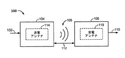
図1は、例示的な一実施形態によるワイヤレス電力伝達システム100の機能ブロック図である。エネルギー伝達を実行するためのワイヤレス場(たとえば、磁場または電磁場)105を生成するために、電力源(この図に示さず)から送電器104に入力電力102が供給され得る。受電器108は、ワイヤレス場105に結合し得、出力電力110に結合されたデバイス(この図に示さず)による蓄積または消費のための出力電力110を生成し得る。送電器104と受電器108の両方は、距離112だけ分離される。
FIG. 1 is a functional block diagram of a wireless
例示的な一実施形態では、送電器104および受電器108は、相互共振関係に従って構成される。受電器108の共振周波数および送電器104の共振周波数が実質的に同じであるか、または極めて近いとき、送電器104と受電器108との間の伝送損失は最小である。したがって、極めて近い(たとえば、場合によっては数ミリメートル内の)大型アンテナコイルを必要とする場合がある純粋に誘導性の解決策とは対照的に、より長い距離にわたってワイヤレス電力伝達が提供され得る。共振誘導結合技法は、様々な距離にわたって様々な誘導コイル構成を用いる、改善された効率および電力伝達をそのように可能にし得る。
In one exemplary embodiment,
送電器104によって生成されたワイヤレス場105に受電器108があるとき、受電器108は電力を受け得る。ワイヤレス場105は、送電器104によって出力されたエネルギーが受電器108によって取り込まれ得る領域に相当する。ワイヤレス場105は、以下でさらに説明するように、送電器104の「近距離場」に相当し得る。送電器104は、エネルギーを受電器108へ送るための送電アンテナまたは送電コイル114を含み得る。受電器108は、送電器104から送られたエネルギーを受けるか、または取り込むための受電アンテナまたは受電コイル118を含み得る。近距離場は、送電コイル114から離れて電力を最小限に放射する送電コイル114における電流および電荷から生じる強い反応場が存在する領域に相当し得る。近距離場は、送電コイル114の約1波長(または、その分数)内である領域に相当し得る。
When there is a
上記で説明したように、効率的なエネルギー伝達は、電磁波におけるエネルギーのほとんどを遠距離場に伝搬させるのではなく、ワイヤレス場105におけるエネルギーの大部分を受電コイル118に結合させることによって行われ得る。ワイヤレス場105内に位置決めされると、送電コイル114と受電コイル118との間に「結合モード」が発達し得る。この結合が起こり得る送電アンテナ114および受電アンテナ118の周囲のエリアは、本明細書で結合モード領域と呼ばれる。
As explained above, efficient energy transfer can be performed by coupling most of the energy in the
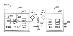
図2は、別の例示的な実施形態によるワイヤレス電力伝達システム200の機能ブロック図である。システム200は、送電器204および受電器208を含む。送電器204は、発振器222、ドライバ回路224、およびフィルタ/整合回路226を含み得る送電回路機構206を含み得る。発振器222は、周波数制御信号223に応答して調整され得る所望の周波数において信号を生成するように構成され得る。発振器222は、発振器信号をドライバ回路224に供給し得る。ドライバ回路224は、入力電圧信号(VD)225に基づいて、たとえば、送電アンテナ214の共振周波数において、送電アンテナ214を駆動するように構成され得る。ドライバ回路224は、発振器222から方形波を受けるとともに正弦波を出力するように構成されたスイッチング増幅器であってよい。
FIG. 2 is a functional block diagram of a wireless
フィルタ/整合回路226は、高調波または他の不要な周波数をフィルタ除去し得、送電器204のインピーダンスを送電アンテナ214に整合させ得る。送電アンテナ214を駆動する結果として、送電アンテナ214は、ワイヤレス場205を生成して、バッテリー236を充電するのに十分なレベルで電力をワイヤレス出力し得る。
Filter /
受電器208は、整合回路232および整流器回路234を含み得る受電回路機構210を含み得る。整合回路232は、受電回路機構210のインピーダンスを受電アンテナ218に整合させ得る。整流器回路234は、図2に示すように、交流(AC)電力入力から直流(DC)電力出力を生成して、バッテリー236を充電し得る。受電器208および送電器204は、追加として、別個の通信チャネル219(たとえば、Bluetooth(登録商標)、Zigbee、セルラーなど)上で通信し得る。受電器208および送電器204は、代替として、ワイヤレス場205の特性を使用するバンド内シグナリングを介して通信してもよい。
The
受電器208は、送電器204によって送られるとともに受電器208によって受けられる電力量が、バッテリー236を充電するのに適切であるかどうかを決定するように構成され得る。送電器204は、エネルギー伝達を行うための直接場結合係数(k)を有する、大部分は非放射の場を生成するように構成され得る。受電器208は、ワイヤレス場205に直接結合し得、受電回路機構210の出力に結合されたバッテリー(または、負荷)236による蓄積または消費のための出力電力を生成し得る。
The
上記で説明したように、送電器204と受電器208の両方は、ある距離だけ分離され、送電器204と受電器208との間の伝送損失を最小限に抑えるように相互共振関係に従って構成され得る。送電アンテナ214および受電アンテナ218が相互に共振し極近傍にあるとき、ワイヤレス電力伝達システム200は、結合係数(結合係数k)が、通常0.3を上回る強結合レジームとして説明され得る。いくつかの実施形態では、送電器204と受電器208との間の結合係数kは、2つの対応するアンテナ間の距離または対応するアンテナのサイズなどのうちの少なくとも1つに基づいて変化し得る。
As explained above, both
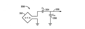
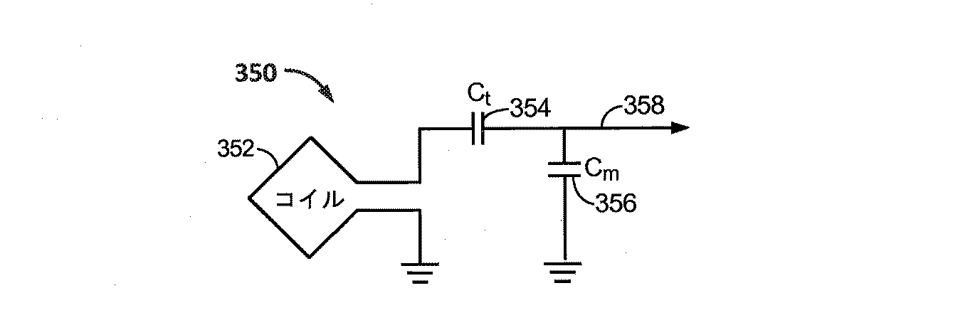
図3は、例示的な実施形態による、図2の送電回路機構206または受電回路機構210の一部分の概略図である。図3に示すように、送電または受電回路機構350は、アンテナ352を含み得る。アンテナ352はまた、「ループ」アンテナ352と呼ばれることがあり、または「ループ」アンテナ352として構成され得る。アンテナ352はまた、「磁気」アンテナもしくは誘導コイルと本明細書で呼ばれることがあり、または「磁気」アンテナもしくは誘導コイルとして構成され得る。「アンテナ」という用語は、一般に、別の「アンテナ」に結合するためのエネルギーをワイヤレスに出力しまたは受けることができる構成要素を指す。アンテナは、電力をワイヤレスに出力しまたは受けるように構成されているタイプのコイルと呼ばれることもある。本明細書で使用するとき、アンテナ352は、電力をワイヤレスに出力し、かつ/または受けるように構成されているタイプの「電力伝達構成要素」の一例である。
FIG. 3 is a schematic diagram of a portion of the power
アンテナ352は、空芯、またはフェライトコアなどの物理的コアを含み得る(この図に示さず)。
The
述べたように、送電器104(図2で参照したような送電器204)と受電器108(図2で参照したような受電器208)との間のエネルギーの効率的な伝達は、送電器104と受電器108との間で整合した共振またはほぼ整合した共振の間に行われ得る。しかしながら、送電器104と受電器108との間の共振が整合しないときであっても、効率に影響を及ぼすことがあるがエネルギーは伝達され得る。たとえば、共振が整合しないとき、効率がより低くなり得る。エネルギーの伝達は、エネルギーを送電コイル114から自由空間中に伝搬させるのではなく、送電コイル114(図2で参照したような送電コイル214)のワイヤレス場105(図2で参照したようなワイヤレス場205)から、ワイヤレス場105の近傍に存在する受電コイル118(図2で参照したような受電コイル218)にエネルギーを結合させることによって行われる。
As stated, the efficient transfer of energy between the transmitter 104 (
ループアンテナまたは磁気アンテナの共振周波数は、インダクタンスおよびキャパシタンスに基づく。インダクタンスは単にアンテナ352によって作り出されるインダクタンスであってよいが、所望の共振周波数において共振構造を作り出すために、アンテナのインダクタンスにキャパシタンスが加えられてよい。非限定的な例として、共振周波数において信号358を選択する共振回路を作り出すために、送電または受電回路機構350にキャパシタ354およびキャパシタ356が加えられてよい。したがって、より大きい直径のアンテナの場合、共振を持続させるのに必要とされるキャパシタンスのサイズは、ループの直径またはインダクタンスが大きくなるにつれて小さくなり得る。
The resonant frequency of the loop antenna or magnetic antenna is based on inductance and capacitance. The inductance may simply be the inductance created by the
さらに、アンテナの直径が大きくなるにつれて、近距離場の効率的なエネルギー伝達エリアが広くなり得る。他の構成要素を使用して形成された他の共振回路も可能である。別の非限定的な例として、キャパシタは、回路機構350の2つの端子間に並列に配置されてもよい。送電アンテナの場合、実質的にアンテナ352の共振周波数に相当する周波数を有する信号358は、アンテナ352への入力であり得る。
Furthermore, as the diameter of the antenna increases, the effective energy transfer area of the near field can be increased. Other resonant circuits formed using other components are possible. As another non-limiting example, a capacitor may be placed in parallel between two terminals of
図1において、送電器104は、送電コイル114の共振周波数に対応する周波数を有する、時間変動する磁場(または、電磁場)を出力し得る。受電器108がワイヤレス場105内にあるとき、時間変動する磁場(または、電磁場)は、受電コイル118において電流を誘導し得る。上記で説明したように、受電コイル118が送電コイル114の周波数で共振するように構成されている場合、エネルギーは効率的に伝達され得る。負荷を充電するかまたは負荷に電力供給するために供給され得るDC信号を生成するために、受電コイル118において誘導されたAC信号は上記で説明したように整流され得る。
In FIG. 1, the
図4は、本発明の例示的な実施形態による、図1のワイヤレス電力伝達システムにおいて使用され得る送電器404の機能ブロック図である。送電器404は、送電回路機構406および送電コイル414を含み得る。送電コイル414は、図3に示すようなコイル352であり得る。送電回路機構406は、送電コイル414の周りのエネルギー(たとえば、磁束)を発生させる発振信号を供給することによって、送電コイル414にRF電力を供給し得る。送電器404は、任意の適切な周波数で動作し得る。例として、送電器404は、13.56MHzのISM帯域において動作し得る。
FIG. 4 is a functional block diagram of a
送電回路機構406は、DCからACへの電力伝達の効率が増大または最大化されるような負荷をドライバ回路424に与えるための、固定インピーダンス整合回路409を含み得る。送電回路機構406は、受電器108(図1)に結合されたデバイスの自己ジャミングを防止するためのレベルまで、高調波放射を低減するように構成されたローパスフィルタ(LPF)408をさらに含み得る。他の例示的な実施形態は、限定はしないが、他の周波数を通過させながら特定の周波数を減衰させ、送電コイル414への出力電力またはドライバ回路424によって引き出されるDC電流などの測定可能な送電メトリックに基づいて変化し得る、適応インピーダンス整合を含み得るノッチフィルタを含む異なるフィルタトポロジーを含み得る。送電回路機構406は、発振器423によって決定されるようなRF信号を駆動するように構成されたドライバ回路424をさらに含む。送電回路機構406は、個別のデバイスもしくは回路から構成されてよく、または代替的に、一体型アセンブリから構成されてもよい。送電コイル414から出力される例示的なRF電力は、2.5ワット程度などの、1ワット〜10ワット程度であってよい。
The
送電回路機構406は、発振器423の周波数または位相を調整するために、かつ取り付けられたそれらの受電器を通じて隣接デバイスと対話するための通信プロトコルを実施するために出力電力レベルを調整するために、特定の受電器用の送電フェーズ(または、デューティサイクル)中に発振器423を選択的に有効化するためのコントローラ415をさらに含み得る。コントローラ415が本明細書でプロセッサ415と呼ばれる場合もあることに留意されたい。発振器位相および送電経路の中の関係する回路機構の調整により、特に、ある周波数から別の周波数に遷移するときの帯域外放射の低減が可能になり得る。
The
送電回路機構406は、送電コイル414によって生成された近距離場の近傍におけるアクティブな受電器の存在または不在を検出するための負荷感知回路416をさらに含み得る。例として、負荷感知回路416は、以下でさらに説明するように、送電コイル414によって生成される場の近傍におけるアクティブな受電器の存在または不在によって影響を及ぼされ得る、ドライバ回路424に流れる電流を監視する。ドライバ回路424における装荷に対する変化の検出は、エネルギーを送るために発振器423を有効化すべきかどうか、およびアクティブな受電器と通信すべきかどうかを決定する際に使用するために、コントローラ415によって監視される。以下でより十分に説明するように、ドライバ回路424において測定される電流は、無効なデバイスが送電器404のワイヤレス電力伝達領域内に位置決めされているかどうかを決定するために使用され得る。
The power
送電コイル414は、リッツ線を用いて実装されてよく、または抵抗損を低く保つように選択された厚さ、幅、および金属タイプを有するアンテナストリップとして実装されてもよい。一実施形態では、送電コイル414は、一般に、テーブル、マット、ランプ、または他のより可搬性が低い構成などの、より大きい構造物と関連するために構成され得る。したがって、送電コイル414は、一般に、実用的な寸法にするための「巻き(turn)」を必要としなくてよい。送電コイル414の例示的な実施形態は、「電気的に小型」(すなわち、波長の分数)であってよく、共振周波数を規定するためにキャパシタを使用することにより、使用可能なより低い周波数で共振するように同調され得る。
The
送電器404は、送電器404に関連し得る受電器デバイスの所在および状態についての情報を収集および追跡し得る。したがって、送電回路機構406は、(本明細書でプロセッサとも呼ばれる)コントローラ415に接続された、存在検出器480、密閉検出器460、またはそれらの組合せを含み得る。コントローラ415は、存在検出器480および密閉検出器460からの存在信号に応答して、ドライバ回路424によって供給される電力量を調整し得る。送電器404は、たとえば、ビルの中に存在する従来のAC電力を変換するためのAC-DC変換器(図示せず)、従来のDC電力源を送電器404にとって適切な電圧に変換するためのDC-DC変換器(図示せず)などのいくつかの電力源を通じて電力を受けてよく、または従来のDC電力源(図示せず)から直接電力を受けてもよい。
The
非限定的な例として、存在検出器480は、送電器404のカバレージエリアに挿入されている充電されるべきデバイスの最初の存在を感知するために利用される運動検出器であり得る。検出後、送電器404はオンにされてよく、所定の方法でRXデバイス上のスイッチをトグルするために、デバイスによって受けられたRF電力が使用されてよく、それにより、送電器404の駆動点インピーダンスへの変化が生じる。
As a non-limiting example,
別の非限定的な例として、存在検出器480は、たとえば、赤外線検出手段、運動検出手段、または他の適切な手段によって人を検出することが可能な検出器であってよい。いくつかの例示的な実施形態では、送電コイル414が特定の周波数で送り得る電力量を制限する規制があり得る。場合によっては、これらの規制は、人を電磁放射から保護することを意図している。しかしながら、たとえば、ガレージ、工場の現場、店舗などの、人によって占有されないか、または人によって占有される頻度が低いエリアの中に、送電コイル414が配置されている環境があり得る。これらの環境に人がいない場合、通常の電力制限規制を超えて送電コイル414の電力出力を増大させることが許容されてよい。言い換えれば、コントローラ415は、人の存在に応答して送電コイル414の電力出力を規制レベルまたはそれ未満に調整してよく、人が送電コイル414の電磁場から規制距離の外側にいるとき、送電コイル414の電力出力を規制レベルを超えるレベルに調整してもよい。
As another non-limiting example,
非限定的な例として、密閉検出器460(本明細書で密閉区画検出器または密閉空間検出器と呼ばれることもある)は、いつ筐体が閉状態または開状態にあるのかを決定するための感知スイッチなどのデバイスであってよい。密閉された状態にある筐体の中に送電器があるとき、送電器の電力レベルは増大されてよい。 As a non-limiting example, a hermetic detector 460 (sometimes referred to herein as a hermetic compartment detector or hermetic space detector) is used to determine when the enclosure is in a closed or open state. It may be a device such as a sensing switch. When the power transmitter is in a sealed enclosure, the power level of the power transmitter may be increased.
例示的な実施形態では、それによって送電器404が無期限にオンのままにならない方法が使用され得る。この場合、送電器404は、ユーザが決定した量の時間の後に停止するようにプログラムされ得る。この機能は、送電器404、特にドライバ回路424が、その周囲にあるワイヤレスデバイスが十分に充電された後、長く動作することを防止する。この事象は、中継器または受電コイルのいずれかから送られる、デバイスが十分に充電されているという信号を回路が検出しないことに起因し得る。送電器404がその周囲に別のデバイスが配置されている場合に自動的に停止することを防止するために、送電器404の自動停止機能は、その周囲で運動が検出されないものとして設定された期間の後にのみ活動化され得る。ユーザは、非アクティビティ時間間隔を決定し必要に応じてそれを変更することができる場合がある。非限定的な例として、その時間間隔は、特定のタイプのワイヤレスデバイスが最初に十分に放電されているという仮定の下で、そのデバイスを十分に充電するのに必要とされる時間間隔よりも長くてよい。
In an exemplary embodiment, a method may be used whereby the
図5は、本発明の例示的な実施形態による、図1のワイヤレス電力伝達システムにおいて使用され得る受電器508の機能ブロック図である。受電器508は、受電コイル518を含み得る受電回路機構510を含む。受電器508は、受けた電力をそこに供給するためのデバイス550にさらに結合する。受電器508は、デバイス550の外部にあるものとして示されるが、デバイス550に統合されてもよいことに留意されたい。エネルギーは、受電コイル518にワイヤレスに伝搬され得、次いで、受電回路機構510の残部を通じてデバイス550に結合され得る。例として、充電デバイスは、モバイルフォン、ポータブル音楽プレーヤ、ラップトップコンピュータ、タブレットコンピュータ、コンピュータ周辺デバイス、通信デバイス(たとえば、Bluetooth(登録商標)デバイス)、デジタルカメラ、補聴器(および、他の医療デバイス)などのデバイスを含み得る。
FIG. 5 is a functional block diagram of a
受電コイル518は、送電コイル414(図4)と同じ周波数で、または特定の周波数範囲内で共振するように同調され得る。受電コイル518は、送電コイル414と類似の寸法であってよく、または関連するデバイス550の寸法に基づいて異なってサイズ決定されてもよい。例として、デバイス550は、送電コイル414の直径または長さよりも短い直径寸法または長さ寸法を有するポータブル電子デバイスであってよい。そのような例では、受電コイル518は、同調キャパシタ(図示せず)のキャパシタンス値を低減させ、受電コイルのインピーダンスを増大させるために、多巻きコイルとして実装され得る。例として、受電コイル518は、コイルの直径を最大化し、受電コイル518のループ巻き数(すなわち、巻回)および巻線間キャパシタンスを低減するために、デバイス550の実質的な外周の周りに配置されてよい。
The
受電回路機構510は、受電コイル518へのインピーダンス整合をもたらし得る。受電回路機構510は、受けたRFエネルギー源をデバイス550が使用するための充電電力に変換するための電力変換回路機構506を含む。電力変換回路機構506は、RF-DC変換器520を含み、またDC-DC変換器522を含み得る。RF-DC変換器520は、受電コイル518において受けたRFエネルギー信号を、Vrectによって表される出力電圧を有する非交流電力に整流する。DC-DC変換器522(または、他の電力レギュレータ)は、整流されたRFエネルギー信号を、VoutおよびIoutによって表される出力電圧および出力電流を有する、デバイス550に適合するエネルギー電位(たとえば、電圧)に変換する。部分整流器および完全整流器、レギュレータ、ブリッジ、ダブラ、ならびにリニア変換器およびスイッチング変換器を含む、様々なRF-DC変換器が企図される。
The power
受電回路機構510は、受電コイル518を電力変換回路機構506に接続するための、または代替的に、電力変換回路機構506を切断するための、スイッチング回路機構512をさらに含み得る。電力変換回路機構506から受電コイル518を切断することは、デバイス550の充電を中断するだけでなく、送電器404(図2)によって「見られる」ような「負荷」も変化させる。
The power
上記で開示したように、送電器404は、送電器ドライバ回路424に供給されるバイアス電流の変動を検出し得る負荷感知回路416を含む。したがって、送電器404は、いつ受電器が送電器の近距離場の中に存在するのかを決定するための機構を有する。
As disclosed above, the
いくつかの実施形態では、受電器508は、近くの他の受電器への結合を除去するか、または近くの送電器における装荷を低減させるためにクローキングされ得る。受電器のこの「除荷」は、本明細書で「クローキング」とも呼ばれる。さらに、受電器508によって制御され送電器404によって検出される、除荷と装荷との間のこのスイッチングは、以下でより十分に説明するように、受電器508から送電器404への通信機構を提供し得る。加えて、受電器508から送電器404へメッセージを送ることを可能にするスイッチングに、プロトコルが関連付けられ得る。例として、スイッチング速度は、100μ秒程度であってよい。
In some embodiments, the
例示的な実施形態では、送電器404と受電器508との間の通信は、従来の双方向通信(すなわち、結合場を使用する帯域内シグナリング)ではなく、デバイス感知および充電制御機構を指す。言い換えれば、送電器404は、エネルギーが近距離場の中で利用可能であるかどうかを調整するために、送られる信号のオン/オフキーイングを使用し得る。受電器は、エネルギーのこれらの変化を送電器404からのメッセージとして解釈し得る。受電器側からは、どれくらいの電力が場から受け入れられているのかを調整するために、受電器508が受電コイル518の同調および離調を使用し得る。場合によっては、同調および離調は、スイッチング回路機構512を介して実現されてよい。送電器404は、場からの使用される電力のこの差を検出し得、これらの変化を受電器508からのメッセージとして解釈し得る。送信電力の変調および負荷挙動の他の形態が利用され得ることに留意されたい。
In the exemplary embodiment, communication between
受電回路機構510は、送電器から受電器への情報のシグナリングに相当し得る、受けたエネルギーの変動を識別するために使用される、シグナリング検出器/ビーコン回路機構514をさらに含み得る。さらに、受電回路機構510をワイヤレス充電用に構成するために、低減されたRF信号エネルギー(すなわち、ビーコン信号)の送信を検出し、低減されたRF信号エネルギーを、受電回路機構510内の電力供給されないかまたは電力が枯渇したかのいずれかの回路を呼び起こすための公称電力に整流するためにも、シグナリング/ビーコン回路機構514が使用され得る。
The
受電回路機構510は、本明細書で説明するスイッチング回路機構512の制御を含む、本明細書で説明する受電器508の処理を調整するためのプロセッサ516をさらに含む。受電器508のクローキングはまた、充電電力をデバイス550に供給する外部の有線充電ソース(たとえば、壁/USB電力)の検出を含む、他の事象が発生すると起こり得る。プロセッサ516はまた、受電器のクローキングを制御することに加えて、シグナリング検出器/ビーコン回路機構514を監視してビーコン状態を決定し、送電器404から送られたメッセージを抽出し得る。プロセッサ516はまた、性能を改善するためにDC-DC変換器522を調整し得る。
The
図6は、図4の送電回路機構406において使用され得る送電回路機構600の一部分の概略図である。送電回路機構600は、図4において上記で説明したようなドライバ回路624を含み得る。上記で説明したように、ドライバ回路624は、方形波を受けるとともに送電回路650に供給されるべき正弦波を出力するように構成され得るスイッチング増幅器であり得る。場合によっては、ドライバ回路624は、増幅器回路と呼ばれることがある。ドライバ回路624はE級増幅器として示されるが、任意の適切なドライバ回路624が本発明の実施形態に従って使用されてよい。ドライバ回路624は、図4に示すような発振器423からの入力信号602によって駆動され得る。ドライバ回路624はまた、送電回路650を通じて供給され得る最大電力を制御するように構成されている駆動電圧VDが供給され得る。高調波を除去または低減するために、送電回路機構600は、フィルタ回路626を含み得る。いくつかの実施形態では、フィルタ回路626は、3極(キャパシタ634、インダクタ632、およびキャパシタ636)の低域フィルタ回路626であってよい。
FIG. 6 is a schematic diagram of a portion of a power
フィルタ回路626によって出力された信号は、コイル614を備える送電回路650に供給され得る。送電回路650は、ドライバ回路624によって供給されるフィルタ処理済み信号の周波数で共振し得る、キャパシタンス620およびインダクタンスを有する直列共振回路を含み得る。様々な実施形態では、コイルまたは追加のキャパシタ構成要素が、インダクタンスまたはキャパシタンスを作り出し得る。送電回路650の負荷は、可変抵抗器622によって表され得る。負荷は、送電回路650から電力を受けるように位置決めされたワイヤレス電力受電器508の関数であり得る。
The signal output by the
様々な実施形態では、図1〜図6に関して上記で説明したワイヤレス電力伝送システム100は、近くの物体の検出に基づいて、ワイヤレス電力伝送を変化させ得る。近くの物体は、意図された受電器、充電されるべきデバイス、および/または外来物体を含み得る。外来物体は、たとえば、寄生受電器、無生物物体、または生物(たとえば、人、動物など)などの、意図された送電ターゲット以外の何か(すなわち、非充電デバイス)であり得る。寄生受電器は、たとえば、非電子的な金属物体、無許可の充電可能デバイスなどを含み得る。
In various embodiments, the wireless
たとえば、図4に関して上記で説明したように、送電器404は、近くの物体の存在、距離、配向、および/またはロケーションを検出し得る存在検出器480を含み得る。様々な他の実施形態では、存在検出器480は、たとえば、受電器508上、または他の場所などの別のロケーションにあってもよい。コントローラ415は、最初の距離内で外来物体が検出されたとき、送信電力を低減し得る。様々な実施形態では、ワイヤレス電力伝送システム100は、生物学的な安全性、防火性などに関する規則または規制に従って、ワイヤレス電力伝送の特性を調整し得る。たとえば、ワイヤレス電力伝送システム100は、近くの人体までの距離が与えられると、その人体に届く電磁場がしきい値を下回るように送信電力を調整し得る。
For example, as described above with respect to FIG. 4, the
再び図2を参照すると、いくつかの実施形態では、ワイヤレス電力伝達システム200は、複数の受電器208を含み得る。一実施形態では、TXコイル214のサイズは固定である。したがって、送電器204は、異なるサイズのRXコイル218にうまく整合されないことがある。様々な理由で、送電器204が複数のTXコイル214を使用することが望ましくあり得る。いくつかの実施形態では、複数のTXコイル214は、アレイをなして配置されてよい。いくつかの実施形態では、アレイはモジュール式であってよい。いくつかの実施形態では、アレイは同じかまたは実質的に同じサイズのTXコイル214を含んでよい。
Referring again to FIG. 2, in some embodiments, the wireless
様々な実施形態では、受電器208のロケーションおよび/またはそれらのRXコイル218のサイズに基づいて、各TXコイル214が独立してアクティブにされ得る。たとえば、比較的小さいRXコイル218を有する近くの受電器208に、単一のTXコイル214がワイヤレス電力を供給し得る。一方、比較的大きいRXコイル218を有する近くの受電器に、複数のTXコイル214がワイヤレス電力を供給し得る。RXコイル218の近くにないTXコイル214は、非活動化されてよい。
In various embodiments, each
いくつかの実施形態では、複数のTXコイル214は、広い送電エリアを形成し得る。送電エリアはスケーラブルであってよく、追加のTXコイル214を使用してもっと広いエリアをカバーし得る。TXコイル214は、広いエリアにわたるデバイスの自由な位置決めを可能にし得る。さらに、TXコイル214は、複数の受電器208を同時に充電するように構成され得る。いくつかの実施形態では、個々のTXコイル214は互いに結合し得る。結合されているTXコイル214は、たとえば、近隣の増幅器へ電力を駆動する1つの電力増幅器をもたらし得る。したがって、結合されたTXコイル214は、増幅器の不安定性および/または損傷を引き起こすことがある。互いに極近傍にあり同時にアクティブであるTXコイル214間の相互結合/相互インダクタンスを低減または除去するための方法、システム、および/または装置を、ワイヤレス電力伝達システム100が含むことが望ましくあり得る。
In some embodiments, the plurality of TX coils 214 may form a large power transmission area. The transmission area may be scalable and an
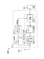
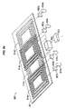
図7aは、例示的な実施形態による例示的な送電エリア700の斜視図である。図示のように、送電エリア700は、4つの送電回路(個々にラベル付けされてはいない)を含む。送電エリア700の送電回路は、それぞれ上記で説明した構成要素(たとえば、コイル、増幅器、共振構成要素)を備える、図1〜図6に関して上記で説明した送電器および/または送電回路機構を備え得る。図4に関して上記で説明したように、送電エリア700の中の送電回路は、第1の電力増幅器(PA)724a、第2のPA724b、第3のPA724c、および第4のPA724dを備え得る。PA724a〜724dは、図4の増幅器すなわちドライバ424に相当し得る。PA724a〜724dは、図3の共振キャパシタ354/356に相当し得るそれぞれの共振キャパシタ702a〜702dに接続されている。送電エリア700は、第1の送電コイル714a、第2の送電コイル714b、第3の送電コイル714c、および第4の送電コイル714d、ならびにすべての送電コイル714a〜714dが接続する共通接地725をさらに含む。送電コイル714a〜714dは、図4の送電コイル414に相当し得る。したがって、送電コイル714a〜714dの第1の端部は、それらそれぞれのPA724a〜724dに接続されており、送電コイル714a〜714dの第2の端部は、共通接地725に接続されている。図7aに示す送電エリア700は4つの送電回路を含むが、他の実施形態では、より多数またはより少数の送電回路(および、それらの関連する構成要素)が送電エリア700に含まれてよい。図示のように、送電コイル714aと714cとのペアは、送電コイル714bと714dとのペアと異なる共通平面に配置され得る。いくつかの実施形態では、共通接地725は、PA724a〜724dと共有され得る。
FIG. 7a is a perspective view of an exemplary
送電コイル714a〜714dは長方形であるものとして示されるが、いくつかの実施形態では、送電コイル714a〜714dは、任意の他の形状(たとえば、三角形、円形、六角形など)であってよい。いくつかの実施形態では、送電コイル714a〜714dは、送電コイルのアレイを形成し得、各送電コイル714a〜714dは、送電エリア700の他の送電コイル714a〜714dに実質的に隣接して位置決めされる。いくつかの実施形態では、送電コイル714a〜714dは、重複する方式で位置決めされてよく、送電コイル714a〜714dの各々は、送電エリア700の中で1つまたは複数の他の送電コイル714a〜714dと重複してよい。さらに、図7aに示す送電コイル714a〜714dは、多巻きコイルである。しかしながら、他の実施形態では、送電コイル714a〜714dは、単巻きコイルであってよく、単層または多層のコイルのいずれかであってよい。いくつかの実施形態では、送電コイル714a〜714dは、インダクタンスが2000nHであり得る。他の実施形態では、送電コイル714a〜714dは、インダクタンスが2000nHよりも大きくまたは小さくてもよい。他の実施形態では、送電コイル714a〜714dの各々は、異なる値のインダクタンスを有してもよく、または送電コイル714a〜714dの様々な組合せが、異なる値のインダクタンスを共有してもよい。
Although the
上記で説明したように、PA724a〜724dおよび送電コイル714a〜714dの各々は個別の送電回路を形成し得、送電回路のいずれも共通接地725の所を除いていかなる点においても接続され得ない。送電回路は、1つまたは複数の受電器または受電回路(図示せず)へ電力および/または通信をワイヤレスに送るためのワイヤレス場(図示せず)を生成するように働く。この図に示さないが、送電回路の各々は共振キャパシタを含み得る。上記で説明したように、図7aに示すように、送電コイル714aと714cとのペアは第1の平面に配置され得、送電コイル714bと714dとのペアは、第1の平面と異なる第2の平面に配置され得る。他の実施形態では、送電回路の4つの送電コイル714a〜714dのうちのいくつかは、回路板の同じ側または両側に配置され得る(すなわち、第1の平面は回路板の表側であってよく、第2の平面は回路板の裏側であってよい)。いくつかの実施形態では、回路板はプリント回路板(PCB701)を備え得る。いくつかの実施形態では、4つの送電コイル714a〜714dは、PCB701の同じ側に配置され得る。いくつかの他の実施形態では、送電コイル714a〜714dのペアは、PCB701の両側に配置され得る。たとえば、送電コイル714aおよび714cがPCB701の片側にあってよく、送電コイル714bおよび714dがPCB701の反対側にあってよい。図示される送電回路の4つの送電コイル714a〜714dは、互いに対して2つの平面(すなわち、PCB701の両側)のうちの1つに実質的に位置して示されるが、他の実施形態では、送電回路の送電コイル714a〜714dは、互いに対してより多数またはより少数の平面(または、層)に配置されてもよい。
As explained above, each of PAs 724a-724d and
送電回路は各々、図4に関して上記で説明したように、PA724a〜724dによって生成される信号に基づいて、関連する送電コイル714a〜714dによってワイヤレス場を生成するように構成され得る。しかしながら、送電回路が他の送電回路と極近傍にある(すなわち、ある送電回路からの送電コイル714aが別の送電回路からの送電コイル714bと極近傍にある)とき、相互インダクタンス(送電コイル714a〜714dの各ペア間での相互結合に起因する)が送電コイル714a〜714dの間に生成されることがある。相互インダクタンスは、あるインダクタ、ここでは送電コイル714aが、別のインダクタ、たとえば、送電コイル714bに及ぼし得る影響であり得、逆も同様である。他の送電コイル714a〜714dと極近傍にある送電コイル714a〜714dの間の相互インダクタンスは、送電コイル714a〜714dのアレイにわたる効率および場均一性に悪影響を有し得る。送電コイル714a〜714dのうちの2つの送電コイルの間の相互インダクタンスの量は、少なくとも部分的には、送電コイル714a〜714dのサイズおよび/または互いに対する送電コイル714a〜714dのロケーションに対応し得る。たとえば、2つの重複する送電コイル714aおよび714bは、送電コイル714aと714bの両方からの磁場が送電コイル714aと714bの両方の中心を同じ方向に通過し得るので、正の相互インダクタンスを有し得る。2つの隣接する送電コイル、たとえば、送電コイル714aおよび714cは、送電コイル714aおよび714cからの磁場が送電コイル714aおよび714cのそれぞれの中心を反対方向に通過し得るので、負の相互インダクタンスを有し得る。
Each of the power transmission circuits may be configured to generate a wireless field by associated
図7bは、例示的な実施形態による例示的な送電エリア700の概略図を示す。図7aに示すように、送電エリア700は、それぞれ個別の分離されたPA724a〜724dを有し相互インダクタンス消去回路または回路機構を伴わない複数の送電コイル714a〜714dを備え得る。図7bに示すように、4つの個別の送電回路がある。4つの送電回路は各々、送電コイル714a〜714dのうちの1つを備え得、送電コイル714a〜714dの各々は、PA724a〜724dにそれぞれ接続されており、電力増幅器724a〜724dとそれぞれの送電コイル714a〜714dとの間に共振キャパシタ702a〜702dを有する。共振キャパシタ702a〜702dは、共振回路を作り出すために、上記で説明したキャパシタ354、357、および/または620のうちの1つまたは複数を含み得る。送電コイル714a〜714dの反対側の端部において、送電コイル714a〜714dの各々は、共通接地725に直接接続されている帰路を有する。したがって、送電コイル714a〜714dの各々は、接地725において互いの送電コイル714a〜714dに接続されている。
FIG. 7b shows a schematic diagram of an exemplary
図2に関して上記で説明したように、送電アンテナ214と受電アンテナ218との間での結合が、それぞれ、存在し得るとともに結合係数または結合係数(k)に関係し得る。結合係数の値は、-1〜1で変化し得る。2つのコイル間の相互インダクタンスは、下の式1を使用して計算され得る。
As described above with respect to FIG. 2, the coupling between the transmitting
M=K*(L1*L2)の平方根 (式1) Square root of M = K * (L1 * L2) (Equation 1)
図7aおよび図7bに関して、隣接する送電コイル714a〜714dのうちの1つまたは複数が変動/変化する電流を伴って活動化されている(ワイヤレス場を生成する)とき、隣接または重複する送電コイル714a〜714dの間に相互インダクタンスが生成され得る。たとえば、相互インダクタンスM12は、2つの送電コイル714a〜714bのうちの少なくとも1つがアクティブであるときに送電コイル714aと714bとの間に作り出される相互インダクタンスを表し得る。同様に、相互インダクタンスM23は、送電コイル714bと714cとの間に作り出される相互インダクタンスを表し得、相互インダクタンスM13は、送電コイル714aと714cとの間の相互インダクタンスを表し得る。相互インダクタンスM34は、送電コイル714cおよび714dのうちの少なくとも1つがそれらを通る電流フローを有するときに送電コイル714cと714dとの間に生成される相互インダクタンスを表し得る。相互インダクタンスM14は、送電コイル714aおよび714dのうちの1つまたは複数の動作中に生成される相互インダクタンスを表し、相互インダクタンスM24は、送電コイル714bと714dとの間に生成される相互インダクタンスを表す。
7a and 7b, adjacent or overlapping power transmission coils when one or more of the adjacent
上記で説明したように、図7bに示す構成要素に照らして下のTable 1(表1)における例示的な値に示すように、送電コイル714a〜714dの様々な組合せの間の相互インダクタンスに関連する結合係数は、送電コイル714a〜714dがそれぞれほぼ同じサイズであるとき、送電コイル714a〜714dのうちの2つの間の距離に基づいて変化し得る。以下に示す結合係数(k)値は、インダクタンスが2000nHの送電コイル714a〜714dと、キャパシタンスが276pFの共振キャパシタ702a〜702dとを備える、ワイヤレス電力伝達システム100に基づき得る。いくつかの実施形態では、これらのインダクタンスまたはキャパシタンスのいずれかは、異なる値の場合があり、相互結合係数値(k)を変化させることがある。
As described above, in relation to the mutual inductance between various combinations of
隣接する送電コイル714a〜714dの間のこれらの相互インダクタンス結合係数は、下のTable 2(表2)における例示的な値に示すような、図示の送電コイル714a〜714dの組合せの間の相互インダクタンスに対応し得る。
These mutual inductance coupling coefficients between
図7cは、例示的な実施形態による、互いに関係する送電エリア700の送電コイル714a〜714cのレイアウトの水平方向の図を示す。図7cに示すように、送電エリア700は、送電コイル714a、送電コイル714b、および送電コイル714cを含む。2つの送電コイル714aおよび714bは、重複するレイアウトで示され(すなわち、送電コイル714aの少なくとも一部分が送電コイル714bの少なくとも一部分と重複する)、送電コイル714bおよび714cも重複する。距離s1は、2つの送電コイル714aと714bとの間の重複の量を示す。距離s2は、重複する2つの送電コイル714aと714bとの間のy方向での距離を示し、それらが水平方向で重複するときの重複する2つの送電コイル714aと714bとの間の高さの差分を表し得る。いくつかの実施形態では、送電コイル714aおよび714bがPCB701の両側に配置されるとき、距離s2はPCB701の厚さに相当し得る。重複の距離s1は、2つの送電コイル714aおよび714bのサイズに基づく可変の距離であり得る。重複の距離s2は、2つの送電コイル714aおよび714bがその上に取り付けられ得る基板(すなわち、プリント回路板(PCB701))の厚さに基づく可変の距離であり得る。受電器(図示せず)は、送電コイル714a〜714dの上方に、設計されているワイヤレス電力伝達用途に基づく距離において配置され得る。たとえば、大電力ワイヤレス電力伝達(たとえば、電気車両充電用のワイヤレス電力伝達)の場合、受電器と送電コイル714a〜714dとの間の距離は、低電力ワイヤレス電力伝達用途(たとえば、モバイルデバイスのワイヤレス充電)よりも長くなり得る。
FIG. 7c shows a horizontal view of the layout of the
図7cに示すように、2つの送電コイル714aおよび714cは、隣接するレイアウトで示される(すなわち、送電コイル714aおよび714cは重複せず、同じy軸平面にある)。距離s3は、2つの送電コイル714aと714cとの間の距離を示す。この図に示さないが、送電コイル714aおよび714cは、異なるy軸平面にあってよい。距離s3は、2つの送電コイル714aおよび714cのサイズ、ならびに/または送電エリア700にとってのワイヤレス電力伝達用途に基づく可変の距離であり得る。
As shown in FIG. 7c, the two
図8aは、例示的な実施形態による例示的な送電エリア800の斜視図である。図示のように、送電エリア800は4つの送電回路を含む。送電エリア800の送電回路は、図1〜図6に関して上記で説明した送電器および/または送電回路機構を備え得る。送電回路は、第1の電力増幅器(PA)824a、第2のPA824b、第3のPA824c、および第4のPA824dを備える。PA824a〜824dは、送電コイル814a〜814dに給電する前に、それぞれの共振キャパシタ802a〜802dに接続されている。送電エリア800は、第1の送電コイル814a、第2の送電コイル814b、第3の送電コイル814c、および第4の送電コイル814d、消去回路809、ならびにすべての送電コイル814a〜814dが消去回路809を通じて接続する共通接地825をさらに含む。したがって、送電コイル814a〜814dの第1の端部は、それらそれぞれのPA824に接続されており、送電コイル814a〜814dの第2の端部は、消去回路809を通じて共通接地825に接続されている。図8aに示す送電エリア800は4つの送電回路を含むが、他の実施形態では、より多数またはより少数の送電回路(および、それらの関連する構成要素)が送電エリア800に含まれてよい。いくつかの実施形態では、共通接地825はまた、PA824a〜824dのうちの1つまたは複数と共有され得る。
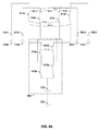
FIG. 8a is a perspective view of an exemplary
送電コイル814a〜814dは長方形であるものとして示されるが、いくつかの実施形態では、送電コイル814a〜814dは、任意の他の形状(たとえば、三角形、円形、六角形など)であってよい。いくつかの実施形態では、送電コイル814a〜814dは、送電コイルのアレイを形成し得、各送電コイル814a〜814dは、送電エリア800の他の送電コイル814a〜814dに実質的に隣接して位置決めされる。いくつかの実施形態では、送電コイル814a〜814dは、重複する方式で位置決めされてよく、送電コイル814a〜814dの各々は、送電エリア800の中で1つまたは複数の他の送電コイル814a〜814dと重複してよい。さらに、図8aに示す送電コイル814a〜814dは、多巻きコイルである。しかしながら、他の実施形態では、送電コイル814a〜814dは、単巻きコイルであってよく、単層または多層のコイルのいずれかであってよい。いくつかの実施形態では、送電コイル814a〜814dは、インダクタンスが2000nHであり得る。他の実施形態では、送電コイル814a〜814dは、インダクタンスが2000nHよりも大きくまたは小さくてもよい。他の実施形態では、送電コイル814a〜814dの各々は、異なる値のインダクタンスを有してもよく、または送電コイル814a〜814dの様々な組合せが、異なる値のインダクタンスを共有してもよい。
Although the
上記で説明したように、PA824a〜824dおよび送電コイル814a〜814dの各々は個別の送電回路を形成し得、送電回路のいずれも共通接地825の所および消去回路809の接続の所を除いていかなる点においても接続され得ない。送電回路は、1つまたは複数の受電器または受電回路(図示せず)へ電力および/または通信をワイヤレスに送るためのワイヤレス場(図示せず)を生成するように働く。この図に示さないが、送電回路の各々は共振キャパシタを含み得る。図示のように、送電回路の4つの送電コイル814a〜814dのうちのいくつかは、回路板の同じ側(すなわち、共面上)または両側に配置され得る。いくつかの実施形態では、4つの送電コイル814a〜814dは、プリント回路板(PCB801)の同じ側に配置され得る。いくつかの他の実施形態では、送電コイル814a〜814dのうちの1つまたは複数(たとえば、ペア)は、PCB801の両側に配置され得る。たとえば、送電コイル814aおよび814cがPCB801の片側にあってよく、送電コイル814bおよび814dがPCB801の反対側にあってよい。図示される送電回路の4つの送電コイル814a〜814dは、互いに対して2つの平面(すなわち、PCB801の両側)のうちの1つに実質的に位置して示されるが、他の実施形態では、送電回路の送電コイル814a〜814dは、互いに対してより多数またはより少数の平面(または、層)に配置されてもよい。さらに、いくつかの実施形態では、PA824a〜824dは、送電コイル814a〜814dおよび関連する回路機構(すなわち、共振キャパシタ802a〜802d)と一緒にPCB801上に配置されてもよい。いくつかの実施形態では、PA824a〜824dは、PCB801に配置されなくてよく、ただし、それらがそれらそれぞれの送電コイル814a〜814dに接続され得るような、PCB801上のコネクタを有してよい。いくつかの実施形態では、消去回路809は、PCB801上に配置され得る(図8aに示すように)。いくつかの実施形態では、共通接地825は、PCB801上に配置されてよく、またはPCB801全体によって共有される接続部であってもよい。
As explained above, each of PAs 824a-824d and
送電回路は各々、図4に関して上記で説明したように、PA824a〜824dによって生成される信号に基づいて、関連する送電コイル814a〜814dによってワイヤレス場を生成するように構成され得る。しかしながら、送電回路が他の送電回路と極近傍にある(すなわち、ある送電回路からの送電コイル814aが別の送電回路からの送電コイル814bと極近傍にある)とき、相互インダクタンス(送電コイル814a〜814dの各ペア間での相互結合に起因する)が送電コイル814a〜814dの間に生成されることがある。消去回路809は、送電コイル814a〜814dの間に生成される相互インダクタンスを低減および/または除去するように構成され得る。消去回路809は、送電コイル814a〜814dの1つもしくは複数のペアの相互インダクタンスまたは送電コイル814a〜814dのすべての相互インダクタンスに加えるか、またはそこから減じるように構成された1つまたは複数の電気構成要素を備え得る。いくつかの実施形態では、消去回路809は、送電コイル814a〜814dのうちの1つまたは複数の相互インダクタンスを補償するために、送電コイル814a〜814dまたは消去回路809のうちの少なくとも1つを移動させるように構成され得る。
Each of the power transmission circuits may be configured to generate a wireless field by associated
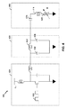
図8bは、例示的な実施形態による、それぞれ個別の分離された電力増幅器を有し相互インダクタンス消去回路を伴う、極近傍にある複数の送電コイルのシステムの概略図を示す。図8aと同様に、図8bは4つの個別の送電回路を示す。4つの送電回路は各々、送電コイル814a〜814dのうちの1つを備え得、送電コイル814a〜814dの各々は、電力増幅器824a〜824dにそれぞれ接続されており、電力増幅器824a〜824dとそれぞれの送電コイル814a〜814dとの間に共振キャパシタを有する。共振キャパシタ802a〜802dは、上記で説明したような共振回路を作り出すために、上記で説明したキャパシタ354および/または357のうちの1つまたは複数を含み得る。送電コイル814a〜814dの反対側の端部において、送電回路の各々は、相互インダクタンス消去回路809を介して共通接地に直接接続されている帰路を有する。消去回路809は、送電コイル814a〜814dのうちの1つまたは複数がアクティブであるとき、近接した送電コイル814a〜814dの間の相互インダクタンスに正または負の相互インダクタンスを加えるように構成された1つまたは複数の電気構成要素を備え得る。消去回路809における電気構成要素の数は、アレイの中の送電コイル814a〜814dの数に少なくとも部分的に基づいて変化し得る。結合されたインダクタおよびキャパシタを様々な配置および構成で使用することによって、正および/または負のインダクタンスが送電コイル814a〜814dの間の相互インダクタンスに取り入れられ得る。
FIG. 8b shows a schematic diagram of a system of multiple transmit coils in close proximity, each with its own separate power amplifier and with a mutual inductance cancellation circuit, according to an exemplary embodiment. Similar to FIG. 8a, FIG. 8b shows four separate power transmission circuits. Each of the four power transmission circuits may comprise one of
消去回路809は、送電コイル814a〜814dのアレイ全体の相互インダクタンスを補償しながら、送電コイル814a〜814dの個々のペア間の相互インダクタンスの補償を可能にし得る。たとえば、インダクタ810aおよび810bは、送電コイル814aと814dとの間にトランスT14を形成する1対の結合されたインダクタを備え得る。送電コイル814aは、送電コイル814dと同様に、インダクタ810aおよび810bによって形成されるトランスを通じて給電する。インダクタ810aおよび810bによって形成されるトランスにより、送電コイル814aおよび814dの相互インダクタンスに寄与することが可能になる。
送電コイル814aおよび814cの電流がインダクタ815aを通じて加算されるように、インダクタ815aは送電コイル814aおよび814cと直列であってよい。送電コイル814bおよび814dの電流がインダクタ815bを通じて加算されるように、インダクタ815bは送電コイル814bおよび814dと直列であってよい。インダクタ815aは、インダクタ810aおよび810bによって形成されるトランスと独立して、送電コイル814aと814cとの間の相互インダクタンスの制御を可能にし得る。同様に、インダクタ815bは、インダクタ810aおよび810bによって形成されるトランスと独立して、送電コイル814bと814dとの間の相互インダクタンスの制御を可能にし得る。インダクタ815aは、送電コイル814aおよび814cの相互インダクタンスにインダクタンスを加え得る。したがって、送電コイル814aと814cとの間の相互インダクタンスが(上記で説明したように)負であるので、これらの2つの送電コイル814aおよび814cと直列のインダクタ815aは、負の相互インダクタンスに正のインダクタンスを加え、この相互インダクタンスを相殺する助けとなる。同様に、インダクタ815bは、送電コイル814bおよび814dが隣接するので(上記で説明したように)負である送電コイル814bおよび814dの相互インダクタンスに、正のインダクタンスを加え得る。したがって、送電コイル814bおよび814dと直列のインダクタ815bからのインダクタンスは、送電コイル814a〜814dの間の相互インダクタンスを相殺する助けとなる。
結合されているインダクタ810aおよび810bは、送電コイル814aと814dとの間に正の相互インダクタンスを加えるように構成され得る。インダクタ815aは、送電コイル814aと814cとの間に正の相互インダクタンスを加えるように構成され得、インダクタ815bは、送電コイル814bと814dとの間に正の相互インダクタンスを加えるように構成され得る。キャパシタ820は、すべての送電コイル814a〜814dの間に負の相互インダクタンスを加えるように構成され得る。いくつかの実施形態では、インダクタおよび/またはキャパシタは、これらのロケーション、または新たなロケーションおよび異なる新たな接続部の間のいずれかにおいて、正または負の相互インダクタンスを加えるように交換され得る。
Coupled
キャパシタ820は、接地まですべての4つの送電コイル814a〜814dと直列である。キャパシタ820は、すべての送電コイル814a〜814dとの間に負のインダクタンスを加え、すべての4つの送電コイル814a〜814dの相互インダクタンスを互いに対してシフトする(0付近の最終センタリング(final centering)として働く)。キャパシタ820は、送電コイル814a〜814dの各々の相互インダクタンスを同じ量だけ変化させるために使用され得る。
図8aおよび図8bに関して、隣接する送電コイル814a〜814dのうちの1つまたは複数が変動/変化する電流を伴って活動化されている(ワイヤレス場を生成する)とき、隣接または重複する送電コイル814a〜814dの間に相互インダクタンスが生成され得る。たとえば、相互インダクタンスM12は、2つの送電コイル814a〜814bのうちの少なくとも1つがアクティブであるときに送電コイル814aと814bとの間に作り出される相互インダクタンスを表し得る。同様に、相互インダクタンスM23は、送電コイル814bと814cとの間に作り出される相互インダクタンスを表し得、相互インダクタンスM13は、送電コイル814aと814cとの間の相互インダクタンスを表し得る。相互インダクタンスM34は、送電コイル814cおよび814dのうちの少なくとも1つがそれらを通る電流フローを有するときに送電コイル814cと814dとの間に生成される相互インダクタンスを表し得る。相互インダクタンスM14は、送電コイル814aおよび814dのうちの1つまたは複数の動作中に生成される相互インダクタンスを表し、相互インダクタンスM24は、送電コイル814bと814dとの間に生成される相互インダクタンスを表す。
8a and 8b, adjacent or overlapping power transmission coils when one or more of the adjacent
上記で説明したように、図8bに示す構成要素に照らして下のTable 3(表3)における例示的な値に示すように、送電コイル814a〜814dの様々な組合せの間の相互インダクタンスに関連する結合係数は、送電コイル814a〜814dがそれぞれほぼ同じサイズであるとき、送電コイル814a〜814dのうちの2つの間の距離に基づいて変化し得る。以下に示す結合係数(k)値は、インダクタンスが2000nHの送電コイル814a〜814dと、キャパシタンスが、それぞれ、258pF、266pF、266pF、および259pFの共振キャパシタ802a〜802dとを備える、ワイヤレス電力伝達システム100に基づき得る。いくつかの実施形態では、これらのインダクタンスまたはキャパシタンスのいずれかは、異なる値の場合があり、相互結合係数値(k)を変化させることがある。さらに、結合されているインダクタ810a〜810bは、インダクタンスが65nH、結合係数が.99であり得、インダクタ815aおよび815bは各々、インダクタンスが110nHであり得る。キャパシタ820は、キャパシタンスが12600pFであり得る。
As described above, in relation to the mutual inductance between various combinations of
隣接する送電コイル814a〜814dの間のこれらの相互インダクタンスは、下のTable 4(表4)における例示的な値に示されるような、図示の送電コイル814a〜814dの組合せの間の相互インダクタンスに対応し得る。
These mutual inductances between adjacent
Table 2(表2)とTable 4(表4)との比較によって示されるように、消去回路809は、送電コイル814a〜814dの様々な組合せの間の相互インダクタンスを消去または大幅に低減しながら、複数の送電コイル814a〜814dが共通接地825を共有することを可能にする。いくつかの実施形態では、消去回路809内の構成要素は、送電コイル814a〜814dの組合せの間の相互インダクタンスの低減を可能にし得るが、相互インダクタンスの除去を可能にし得ない。したがって、いくつかの実施形態では、消去回路809は、複数の送電コイル814a〜814dのうちの1つまたは複数の送電コイル814a〜814dの、x方向またはy方向のうちの少なくとも1つでの、各送電コイル814a〜814dが重複する他の送電コイル814a〜814dに対する平行移動を利用し得る。いくつかの実施形態では、重複する送電コイル814a〜814dを重複の量が増大または減少するように移動させることにより、重複する送電コイル間の相互インダクタンスが増大または減少し得る。
As shown by the comparison between Table 2 and Table 4, the
いくつかの実施形態では、消去回路809自体が、送電コイル814a〜814dに対して異なるロケーションへ移動されてもよい。そのような移動は、送電コイル814a〜814dへの消去回路809の効果に影響を及ぼし得る。たとえば、消去回路809が送電コイル814a〜814dのすべての間で中央に置かれるとき、消去回路809は、消去回路809が4つの送電コイル814a〜814dのアレイの一方の端部または他方の端部に位置決めされるときと異なるように送電コイル814a〜814dと相互作用し得る。
In some embodiments, the
図8cは、例示的な実施形態による、互いに関係する送電エリア800の送電コイル814a〜814cのレイアウトの水平方向の図を示す。図8cのレイアウトおよび構成要素は、図7cに関して上記で説明したものと類似であり、ここで再び説明する必要はない。
FIG. 8c shows a horizontal view of the layout of the
消去回路809の統合は、送電コイル814a〜814dの異なる組合せの相互インダクタンスの独立した制御を可能にし得るので有利であり得る。上記で説明したように、インダクタ810aおよび810bによって形成されるトランスは、送電コイル814aと814dとの間の相互インダクタンスを制御し得、インダクタ815aおよび815bは、それぞれ、送電コイル814aの814cとの相互インダクタンス、および送電コイル814bの814dとの相互インダクタンスを制御し得る。上記で説明したように、キャパシタ820は、送電コイル814a〜814dの各々の相互インダクタンスを同じ量だけ調整することを可能にし得る。したがって、送電コイル814a〜814dの連続的なペア(すなわち、送電コイル814aの814bとのペア、送電コイル814bの814cとのペア、および送電コイル814cの814dとのペア)の相互インダクタンスの調整を可能にする物理的成分(誘導性または静電容量性の)が、消去回路809にあり得ない。しかしながら、送電コイル814a〜814dのこれらのペアの間の相互インダクタンスは、それらそれぞれの重複によって影響を及ぼされ得る(すなわち、送電コイル814aおよび814bの重複が、これらのコイルの間の相互インダクタンスM12に影響を及ぼし得る)。したがって、送電コイル814a〜814dのこれらの連続的なペアの間の相互インダクタンスは、送電コイル814a〜814dまたは消去回路809のうちの少なくとも1つの物理的ロケーション(すなわち、重複)を操作することによって「調整」すなわち補償され得る。たとえば、重複する送電コイル814a〜814dのペアの間の相互インダクタンスを調整するように、送電コイル814a〜814dのペアの重複が変えられてよい。いくつかの実施形態では、送電コイル814a〜814dのペアの重複の操作は、重複する送電コイル814a〜814dの相互インダクタンスのみに影響を及ぼし得る。いくつかの実施形態では、送電コイル814a〜814dの物理的ロケーションおよび重複は、送電エリア800を設計するときに調整され得る。たとえば、近傍にある送電コイル814a〜814dに対する各送電コイル814a〜814dの位置は、送電コイル814a〜814dの間の相互インダクタンスが最小化または低減されるようであってよい。
Integration of the
消去回路809の構成要素を使用して送電コイル814a〜814dの相互インダクタンスを調整することは、相互インダクタンスの「粗」同調として説明され得、送電コイル814a〜814dのペアの重複を調整することは、送電コイル814a〜814dの相互インダクタンスの「最終」同調または「微」同調を備え得る。いくつかの実施形態では、送電コイル814a〜814dの各ペアの個別の制御を可能にするために、追加のインダクタおよび/またはキャパシタが消去回路809に含まれてよい(たとえば、送電コイル814a〜814b、814b〜814c、および814c〜814dのペアの各々と直列にインダクタが導入されてよい)。代替として、上記で説明したように、消去回路809が再配置されてもよく、したがって、送電コイル814a〜814dの相互インダクタンスへの消去回路809の影響を変化させ得る。したがって、インダクタ810a、810b、815a、および815bとキャパシタ820との組合せ、ならびに送電コイル814a〜814dの位置合わせ(重複の調整)および消去回路809の位置合わせが、送電コイル814a〜814dの間の相互インダクタンスの組合せのすべてに対する補償を可能にし得る。
Adjusting the mutual inductance of the
消去回路809のロケーションが変えられると送電コイル814a〜814dの様相が変わるので、消去回路809の物理的ロケーションは、送電コイル814a〜814dの組合せの相互インダクタンスを変え得る。たとえば、送電コイル814a〜814dの長さが、送電コイル814a〜814dの互いへの、かつ消去回路809に対する相互インダクタンスの影響を変え得るので、少なくとも送電コイル814a〜814dの長さは各々、消去回路のロケーションに応じて変わり得る。したがって、いくつかの実施形態では、消去回路809は、送電コイル814a〜814dの様々な組合せの間の相互インダクタンスが最小化または低減されるように送電エリア800にあってよい。
Since the appearance of the
消去回路809を実装することの1つの利点は、送電コイル814a〜814dのアレイの中の個々の送電コイル814a〜814dが、負荷を受けることに従って必要に応じて活動化され得ることである。さらに、送電コイル814a〜814dのアレイが個別の送電コイル814a〜814dに分割され得る(すなわち、各個々の送電コイル814a〜814dが独立に駆動され得る)ので、送電コイル814a〜814dを駆動するPA824a〜824dは、送電コイル814a〜814dのアレイによって見られる任意の負荷を等しく配分し得る(すなわち、図8aのシステム800の場合、4つの送電コイル814a〜814dが4つの独立したPA824a〜824dを伴うことは、必要とされる全電力のうちの4分の1(1/4)しか各PAが生成する必要がないことを意味する)。いくつかの実施形態では、消去回路809は、複数のPA824a〜824dを結合することなく送電コイル814a〜814dを駆動するようにPA824a〜824dのうちの単一のPAを使用して、十分な大電力を供給することを可能にし得る。さらに、送電コイル814a〜814dのアレイに負荷が加えられるとき、消去回路809は、アレイの、近隣にある送電コイル814a〜814dを相互インダクタンスを介して損傷することなく、単一の送電コイル814a〜814dがそれの関連するPA824a〜824dとともに活動化されることを可能にする。したがって、消去回路809は、送電コイル814a〜814dの間の相互インダクタンスを除去することによって、より効率的な電力伝達をもたらし得る。
One advantage of implementing
図9は、例示的な実施形態による、ワイヤレス電力伝送の例示的な方法のフローチャート900である。図1〜図2に関して上記で説明したワイヤレス電力伝送システム100、図4に関して上記で説明した送電器、および図8a〜図8cに関して上記で説明した送電エリア800を参照しながらフローチャート900の方法が本明細書で説明されるが、いくつかの実施形態では、フローチャートの方法は、本明細書で説明する別のデバイス、または任意の他の適切なデバイスによって実施され得る。いくつかの実施形態では、フローチャート900におけるブロックは、たとえば、コントローラ415(図4で参照した)および/またはプロセッサシグナリングコントローラ516(図5で参照した)などの、プロセッサまたはコントローラによって実行され得る。フローチャート900の方法は本明細書で特定の順序を参照しながら説明されるが、様々な実施形態では、本明細書のブロックは、異なる順序で実行されるか、または省略されてよく、さらなるブロックが追加されてもよい。
FIG. 9 is a
ブロック905において、第1のドライバコイル(送電コイル814a〜814dのうちの1つ)が、第1のワイヤレス場を生成する。送電アンテナ814a〜814dのうちのいずれか1つが、第1のワイヤレス場を生成してよい。ワイヤレス場は、電力を別のデバイスへワイヤレスに伝達するため、または別のデバイスとワイヤレスに通信するために使用され得る。ブロック910において、第2のドライバコイル(送電コイル814a〜814dのうちの2番目)が、第2のワイヤレス場を生成する。ブロック915において、第3のドライバコイル(送電コイル814a〜814dのうちの3番目)が、第3のワイヤレス場を生成する。ブロック920において、消去回路809は、それぞれ、第1のドライバコイル、第2のドライバコイル、および第3のドライバコイルによって生成される第1のワイヤレス場、第2のワイヤレス場、および第3のワイヤレス場のうちの少なくとも1つによって生じる相互インダクタンスの少なくとも一部分を消去する。いくつかの実施形態では、上記で説明したように、消去回路は、第1、第2、および第3のワイヤレス場を生成する第1、第2、および第3の送電コイルの各々に正および/または負の相互インダクタンスを加える。いくつかの実施形態では、消去回路809は、送電コイル814a〜814dと直列のインダクタ(すなわち、インダクタ810a〜810bまたは815a〜815b)を使用して、正のインダクタンスを加え得る。いくつかの実施形態では、消去回路809は、送電コイル814a〜814dと直列のキャパシタ(すなわち、キャパシタ820)を使用して、負のインダクタンスを加え得る。いくつかの実施形態では、消去回路809は、送電コイル814a〜814dの相互インダクタンスを微同調させるために、送電コイル814a〜814dまたは消去回路809のうちの少なくとも1つを、x方向またはy方向のうちの少なくとも1つで移動させるようにさらに構成され得る。
At
上記で説明したように、送電コイル814a〜814dは、消去回路809を介して共通接地825に接続することによって、共通接地825を共有し得る。いくつかの実施形態では、共通接地825はまた、送電コイル814a〜814dの各々に接続されている電力増幅器824と共有され得る。いくつかの実施形態では、消去回路809は、正の相互インダクタンスおよび負の相互インダクタンスのうちの少なくとも1つを、少なくとも部分的に消去し得る。いくつかの実施形態では、ドライバコイル(送電コイル814a〜814d)を駆動するために使用される電力増幅器824a〜824dの各々は、隣接するドライバコイル間で90度ステップで互いに位相がずれて駆動され得る。キャパシタ820および/またはインダクタ810a〜810b/815a〜815bは、ドライバコイル(送電コイル814a〜814d)のうちの任意の2つ以上をブリッジし得る。いくつかの実施形態では、2つ以上のインダクタ810a〜810b/815a〜815bからトランスが形成され得る。いくつかの実施形態では、ドライバコイル(送電コイル814a〜814d)は、少なくとも1つの他のドライバコイルと重複するように構成され得る。いくつかの実施形態では、ドライバコイルは、共面上または非共面上に配置され得る。
As described above, the
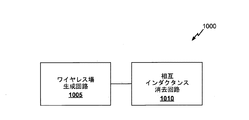
図10は、本発明の例示的な実施形態による、ワイヤレス電力を受電器に伝達するためのシステムの機能ブロック図である。ワイヤレスの電力伝送のために構成されたデバイス1000は、ワイヤレス場を生成するための第1の手段1005、および相互インダクタンス消去手段を備える。いくつかの実施形態では、ワイヤレス場を生成するための手段1005は、ワイヤレス場を生成するための複数の手段を備え得る。
FIG. 10 is a functional block diagram of a system for transferring wireless power to a power receiver, according to an illustrative embodiment of the invention. A
一実施形態では、ワイヤレス場を生成するための第1の手段1005は、ブロック905(図9)に関して上記で説明した機能のうちの1つまたは複数を実行するように構成され得る。様々な実施形態では、ワイヤレス場を生成するための第1の手段1005は、図8a〜図8cの送電コイル814a〜814dのうちの1つまたは複数によって実装され得る。いくつかの実施形態では、ワイヤレス場を生成するための複数の第1の手段1005は、ブロック905(図9)に関して上記で説明した機能のうちの1つまたは複数を実行するように構成され得る。
In one embodiment, the first means 1005 for generating a wireless field may be configured to perform one or more of the functions described above with respect to block 905 (FIG. 9). In various embodiments, the first means 1005 for generating a wireless field may be implemented by one or more of the
相互インダクタンスを消去するための第2の手段1010は、ブロック910(図9)に関して上記で説明した機能のうちの1つまたは複数を実行するように構成され得る。様々な実施形態では、相互インダクタンスを消去するための第2の手段1010は、消去回路809のうちの1つまたは複数によって実装され得る。いくつかの実施形態では、追加の手段が、図9に関して上記で説明したステップのうちの1つまたは複数を実行するように構成され得る。いくつかの実施形態では、電力を増幅するための手段が、ワイヤレス場(図示せず)を生成するために、ワイヤレス場を生成するための手段によって送るための電力を増幅するように構成され得る。いくつかの実施形態では、電力を増幅するための手段は、上記で説明した電力増幅器824a〜824dを備え得る。いくつかの実施形態では、ワイヤレス場を生成するための手段と共通接地を共有するための手段が、ワイヤレス場を生成するための手段を単一の接地に接続するように構成され得る。いくつかの実施形態では、単一の接地は、ワイヤレス場を生成するための手段および電力を増幅するための手段と共有され得る。いくつかの実施形態では、ワイヤレス場を生成するための手段のうちの少なくとも1つの位置を調整するための手段、および/または相互インダクタンスを消去するための手段の位置を調整するための手段が、ワイヤレス場を生成するための手段および/または相互インダクタンスを消去するための手段のうちの少なくとも1つを物理的に移動させるように構成され得る。いくつかの実施形態では、ワイヤレス場を生成するための手段のうちの少なくとも1つの位置を調整するための手段、および/または相互インダクタンスを消去するための手段の位置を調整するための手段は、x方向およびy方向で物理的に移動させるように構成されたx-y平行移動モーターまたは類似のデバイスのうちの1つを備え得る。
Second means 1010 for canceling mutual inductance may be configured to perform one or more of the functions described above with respect to block 910 (FIG. 9). In various embodiments, the
上記で説明した方法の様々な動作は、様々なハードウェアおよび/もしくはソフトウェア構成要素、回路、ならびに/またはモジュールなどの、動作を実行することが可能な任意の適切な手段によって実行され得る。概して、図に示される任意の動作は、動作を実行することが可能な対応する機能的手段によって実行され得る。 Various operations of the methods described above may be performed by any suitable means capable of performing operations, such as various hardware and / or software components, circuits, and / or modules. In general, any operation shown in the figures may be performed by corresponding functional means capable of performing the operation.
様々な異なる技術および技法のうちのいずれかを使用して、情報および信号が表され得る。たとえば、上記の説明全体にわたって参照され得るデータ、命令、コマンド、情報、信号、ビット、シンボル、およびチップは、電圧、電流、電磁波、磁場もしくは磁性粒子、光場もしくは光学粒子、またはそれらの任意の組合せによって表され得る。 Information and signals may be represented using any of a variety of different technologies and techniques. For example, data, instructions, commands, information, signals, bits, symbols, and chips that may be referred to throughout the above description are voltages, currents, electromagnetic waves, magnetic fields or magnetic particles, light fields or optical particles, or any of them Can be represented by a combination.
本明細書で開示する実施形態に関して説明された様々な例示的な論理ブロック、モジュール、回路、およびアルゴリズムステップは、電子ハードウェア、コンピュータソフトウェア、またはその両方の組合せとして実装され得る。ハードウェアおよびソフトウェアのこの互換性を明確に示すために、様々な例示的な構成要素、ブロック、モジュール、回路、およびステップが、概してそれらの機能に関して上記で説明された。そのような機能がハードウェアとして実装されるのか、それともソフトウェアとして実装されるのかは、特定の適用例およびシステム全体に課せられた設計制約によって決まる。説明された機能は特定の適用例ごとに様々な方法で実装され得るが、そのような実装決定は、本発明の実施形態の範囲からの逸脱を引き起こすものと解釈されるべきではない。 Various exemplary logic blocks, modules, circuits, and algorithm steps described in connection with the embodiments disclosed herein may be implemented as electronic hardware, computer software, or a combination of both. To clearly illustrate this interchangeability of hardware and software, various illustrative components, blocks, modules, circuits, and steps have been described above generally in terms of their functionality. Whether such functionality is implemented as hardware or software depends upon the particular application and design constraints imposed on the overall system. Although the described functionality may be implemented in a variety of ways for a particular application, such implementation decisions should not be construed as causing deviations from the scope of embodiments of the invention.
本明細書で開示する実施形態に関して説明された様々な例示的なブロック、モジュール、および回路は、汎用プロセッサ、デジタル信号プロセッサ(DSP)、特定用途向け集積回路(ASIC)、フィールドプログラマブルゲートアレイ(FPGA)もしくは他のプログラマブル論理デバイス、個別ゲートもしくはトランジスタ論理、個別ハードウェア構成要素、または本明細書で説明した機能を実行するように設計されたそれらの任意の組合せで、実装または実行され得る。汎用プロセッサはマイクロプロセッサであり得るが、代替として、プロセッサは、任意の従来のプロセッサ、コントローラ、マイクロコントローラ、またはステートマシンであってよい。プロセッサはまた、コンピューティングデバイスの組合せ、たとえば、DSPとマイクロプロセッサとの組合せ、複数のマイクロプロセッサ、DSPコアと連携する1つもしくは複数のマイクロプロセッサ、または任意の他のそのような構成として実装され得る。 Various exemplary blocks, modules, and circuits described with respect to the embodiments disclosed herein include general purpose processors, digital signal processors (DSPs), application specific integrated circuits (ASICs), field programmable gate arrays (FPGAs). ) Or other programmable logic device, individual gate or transistor logic, individual hardware components, or any combination thereof designed to perform the functions described herein. A general purpose processor may be a microprocessor, but in the alternative, the processor may be any conventional processor, controller, microcontroller, or state machine. The processor is also implemented as a combination of computing devices, eg, a DSP and microprocessor combination, multiple microprocessors, one or more microprocessors in conjunction with a DSP core, or any other such configuration. obtain.
本明細書で開示する実施形態に関して説明された方法またはアルゴリズムおよび機能のステップは、直接ハードウェアで具現化されてよく、プロセッサによって実行されるソフトウェアモジュールで具現化されてよく、またはその2つの組合せで具現化されてもよい。ソフトウェアで実装される場合、機能は、1つもしくは複数の命令もしくはコードとして有形の非一時的コンピュータ可読媒体上に記憶され、または有形の非一時的コンピュータ可読媒体を介して送信され得る。ソフトウェアモジュールは、ランダムアクセスメモリ(RAM)、フラッシュメモリ、読取り専用メモリ(ROM)、電気的プログラマブルROM(EPROM)、電気的消去可能プログラマブルROM(EEPROM)、レジスタ、ハードディスク、リムーバブルディスク、CD ROM、または、当技術分野で知られている任意の他の形態の記憶媒体の中に存在し得る。記憶媒体は、プロセッサが記憶媒体から情報を読み取り、かつ記憶媒体に情報を書き込むことができるように、プロセッサに結合される。代替として、記憶媒体はプロセッサと一体であってもよい。本明細書で使用するディスク(disk)およびディスク(disc)は、コンパクトディスク(disc)(CD)、レーザーディスク(登録商標)(disc)、光ディスク(disc)、デジタル多用途ディスク(disc)(DVD)、フロッピーディスク(disk)、およびブルーレイディスク(disc)を含み、ディスク(disk)は、通常、データを磁気的に再生し、ディスク(disc)は、レーザーを用いてデータを光学的に再生する。上記の組合せも、コンピュータ可読媒体の範囲内に含まれるべきである。プロセッサおよび記憶媒体は、ASICの中に存在してよい。ASICは、ユーザ端末の中に存在してよい。代替として、プロセッサおよび記憶媒体は、ユーザ端末の中で個別構成要素として存在してよい。 The method or algorithm and functional steps described with respect to the embodiments disclosed herein may be implemented directly in hardware, may be implemented in software modules executed by a processor, or a combination of the two. May be embodied. If implemented in software, the functions may be stored as one or more instructions or code on a tangible non-transitory computer readable medium or transmitted via a tangible non-transitory computer readable medium. Software modules can be random access memory (RAM), flash memory, read only memory (ROM), electrically programmable ROM (EPROM), electrically erasable programmable ROM (EEPROM), registers, hard disk, removable disk, CD ROM, or It can reside in any other form of storage medium known in the art. A storage medium is coupled to the processor such that the processor can read information from, and write information to, the storage medium. In the alternative, the storage medium may be integral to the processor. The disc and disc used in this specification are a compact disc (CD), a laser disc (registered trademark) (disc), an optical disc (disc), a digital versatile disc (DVD) ), Floppy disk, and Blu-ray disc, the disk normally reproduces data magnetically, and the disc optically reproduces data using a laser . Combinations of the above should also be included within the scope of computer-readable media. The processor and the storage medium may reside in an ASIC. The ASIC may be present in the user terminal. In the alternative, the processor and the storage medium may reside as discrete components in a user terminal.
本開示を要約するために、本発明のいくつかの態様、利点、および新規の特徴が本明細書で説明された。すべてのそのような利点が、本発明の任意の特定の実施形態に従って実現され得るとは限らないことを理解されたい。したがって、本発明は、本明細書で教示または示唆され得る他の利点を必ずしも実現することなく、本明細書で教示されるような1つの利点または利点のグループを実現または最適化するように具現化または実行され得る。 In order to summarize the present disclosure, several aspects, advantages and novel features of the present invention have been described herein. It should be understood that not all such advantages may be realized in accordance with any particular embodiment of the invention. Thus, the present invention may be implemented to realize or optimize one advantage or group of advantages as taught herein without necessarily realizing other advantages that may be taught or suggested herein. Or can be implemented.
上記で説明した実施形態の様々な修正が容易に明らかになり、本明細書で定義される一般原理は、本発明の趣旨または範囲を逸脱することなく他の実施形態に適用され得る。したがって、本発明は、本明細書で示される実施形態に限定されることを意図しておらず、本明細書で開示する原理および新規の特徴と一致する最も広い範囲を与えられるものとする。 Various modifications to the embodiments described above will be readily apparent and the general principles defined herein may be applied to other embodiments without departing from the spirit or scope of the invention. Accordingly, the present invention is not intended to be limited to the embodiments shown herein but is to be accorded the widest scope consistent with the principles and novel features disclosed herein.
100 ワイヤレス電力伝達システム
102 入力電力
104 送電器
105 ワイヤレス場
108 受電器
110 出力電力
114 送電コイル
118 受電コイル
200 ワイヤレス電力伝達システム
204 送電器
205 ワイヤレス場
206 送電回路機構
208 受電器
210 受電回路機構
214 送電アンテナ
218 受電アンテナ
219 別個の通信チャネル
222 発振器
223 周波数制御信号
224 ドライバ回路
225 入力電圧信号
226 フィルタ/整合回路
232 整合回路
234 整流器回路
236 バッテリー
350 送電または受電回路機構
352 アンテナ
354 キャパシタ
356 キャパシタ
404 送電器
406 送電回路機構
408 ローパスフィルタ(LPF)
409 インピーダンス整合回路
414 送電コイル
415 コントローラ
416 負荷感知回路
423 発振器
424 ドライバ回路
460 密閉検出器
480 存在検出器
506 電力変換回路機構
508 受電器
510 受電回路機構
512 スイッチング回路機構
514 シグナリング検出器/ビーコン回路機構
516 プロセッサ
518 受電コイル
520 RF-DC変換器
522 DC-DC変換器
550 デバイス
600 送電回路機構
602 入力信号
614 コイル
620 キャパシタンス
622 可変抵抗器
624 ドライバ回路
626 フィルタ回路
632 インダクタ
634 キャパシタ
636 キャパシタ
650 送電回路
700 送電エリア
701 プリント回路板
702 共振キャパシタ
714 送電コイル
724 電力増幅器(PA)
725 共通接地
800 送電エリア
801 プリント回路板
802 共振キャパシタ
809 消去回路
810 インダクタ
814 送電コイル
815 インダクタ
820 キャパシタ
824 電力増幅器(PA)
825 共通接地
1005 ワイヤレス場を生成するための手段
1010 相互インダクタンスを消去するための手段
100 wireless power transfer system
102 Input power
104 power transmitter
105 Wireless field
108 Power receiver
110 Output power
114 Power transmission coil
118 Power receiving coil
200 wireless power transfer system
204 Power transmitter
205 Wireless field
206 Power transmission circuit mechanism
208 Power receiver
210 Power receiving circuit mechanism
214 Power transmission antenna
218 Power receiving antenna
219 Separate communication channels
222 Oscillator
223 Frequency control signal
224 Driver circuit
225 Input voltage signal
226 Filter / matching circuit
232 matching circuit
234 Rectifier circuit
236 battery
350 Transmission or reception circuit mechanism
352 antenna
354 capacitors
356 capacitors
404 power transmitter
406 Power transmission circuit mechanism
408 Low-pass filter (LPF)
409 Impedance matching circuit
414 Power transmission coil
415 controller
416 Load sensing circuit
423 oscillator
424 Driver circuit
460 Sealed detector
480 Presence detector
506 Power conversion circuit mechanism
508 power receiver
510 Power receiving circuit mechanism
512 Switching circuit mechanism
514 Signaling detector / beacon circuitry
516 processor
518 Power receiving coil
520 RF-DC converter
522 DC-DC converter
550 devices
600 Power transmission circuit mechanism
602 Input signal
614 coil
620 capacitance
622 variable resistor
624 Driver circuit
626 Filter circuit
632 inductor
634 capacitors
636 capacitor
650 power transmission circuit
700 Power transmission area
701 printed circuit board
702 Resonant capacitor
714 power transmission coil
724 Power Amplifier (PA)
725 Common ground
800 Power transmission area
801 printed circuit boards
802 Resonant capacitor
809 Erase circuit
810 inductor
814 Power transmission coil
815 inductor
820 capacitors
824 Power Amplifier (PA)
825 Common ground
1005 Means for generating wireless fields
1010 Means for eliminating mutual inductance
Claims (30)
第1のドライバコイルと、
第2のドライバコイルと、
第3のドライバコイルと、
前記第1のドライバコイル、前記第2のドライバコイル、および前記第3のドライバコイルに動作可能に結合され、前記第1のドライバコイル、前記第2のドライバコイル、および前記第3のドライバコイルの間の相互インダクタンスを少なくとも部分的に消去するように構成された回路とを備え、前記第1、第2、および第3のドライバコイルが、前記回路を介して共通接地を共有するように構成される、
デバイス。 A device configured to send wireless power to a first power receiver,
A first driver coil;
A second driver coil;
A third driver coil;
The first driver coil, the second driver coil, and the third driver coil are operably coupled to the first driver coil, the second driver coil, and the third driver coil. And a circuit configured to at least partially eliminate mutual inductance between the first, second, and third driver coils configured to share a common ground through the circuit. The
device.
第1のドライバコイルを介して第1のワイヤレス場を生成するステップと、
第2のドライバコイルを介して第2のワイヤレス場を生成するステップと、
第3のドライバコイルを介して第3のワイヤレス場を生成するステップと、
前記第1のドライバコイル、前記第2のドライバコイル、および前記第3のドライバコイルに動作可能に結合され、前記第1のドライバコイル、前記第2のドライバコイル、および前記第3のドライバコイルの間の相互インダクタンスを少なくとも部分的に消去するように構成された消去回路を介して、前記第1のワイヤレス場、前記第2のワイヤレス場、および前記第3のワイヤレス場のうちの少なくとも1つによって生じる相互インダクタンスの少なくとも一部分を消去するステップと
を備える方法。 A method for sending wireless power to a receiver,
Generating a first wireless field via a first driver coil;
Generating a second wireless field via a second driver coil;
Generating a third wireless field via a third driver coil;
The first driver coil, the second driver coil, and the third driver coil are operably coupled to the first driver coil, the second driver coil, and the third driver coil. By at least one of the first wireless field, the second wireless field, and the third wireless field via an erasure circuit configured to at least partially erase the mutual inductance between Eliminating at least a portion of the resulting mutual inductance.
第1のワイヤレス場を生成するための手段と、
第2のワイヤレス場を生成するための手段と、
第3のワイヤレス場を生成するための手段と、
前記第1のワイヤレス場生成手段、前記第2のワイヤレス場生成手段、および前記第3のワイヤレス場生成手段に動作可能に結合され、前記第1のワイヤレス場生成手段、前記第2のワイヤレス場生成手段、および前記第3のワイヤレス場生成手段の間の相互インダクタンスを少なくとも部分的に消去するように構成された、相互インダクタンスを消去するための手段とを備え、前記第1、第2、および第3のワイヤレス場生成手段が、共通接地を共有するように構成される、
デバイス。 A device configured to send wireless power to a first power receiver,
Means for generating a first wireless field;
Means for generating a second wireless field;
Means for generating a third wireless field;
Operatively coupled to the first wireless field generating means, the second wireless field generating means, and the third wireless field generating means, wherein the first wireless field generating means, the second wireless field generating Means for erasing the mutual inductance configured to at least partially eliminate the mutual inductance between the third wireless field generating means, and the first, second, and second Three wireless field generating means are configured to share a common ground;
device.
Applications Claiming Priority (3)
| Application Number | Priority Date | Filing Date | Title |
|---|---|---|---|
| US14/524,944 US9780572B2 (en) | 2014-10-27 | 2014-10-27 | Wireless power multi-coil mutual induction cancellation methods and apparatus |
| US14/524,944 | 2014-10-27 | ||
| PCT/US2015/053495 WO2016069185A1 (en) | 2014-10-27 | 2015-10-01 | Wireless power multi-coil mutual induction cancellation methods and apparatus |
Publications (3)
| Publication Number | Publication Date |
|---|---|
| JP2017536070A true JP2017536070A (en) | 2017-11-30 |
| JP2017536070A5 JP2017536070A5 (en) | 2018-10-25 |
| JP6666338B2 JP6666338B2 (en) | 2020-03-13 |
Family
ID=54345588
Family Applications (1)
| Application Number | Title | Priority Date | Filing Date |
|---|---|---|---|
| JP2017519488A Expired - Fee Related JP6666338B2 (en) | 2014-10-27 | 2015-10-01 | Method and apparatus for wireless power multi-coil mutual induction cancellation |
Country Status (5)
| Country | Link |
|---|---|
| US (1) | US9780572B2 (en) |
| EP (1) | EP3213331A1 (en) |
| JP (1) | JP6666338B2 (en) |
| CN (1) | CN107112813B (en) |
| WO (1) | WO2016069185A1 (en) |
Cited By (2)
| Publication number | Priority date | Publication date | Assignee | Title |
|---|---|---|---|---|
| KR20190069698A (en) * | 2017-12-12 | 2019-06-20 | 한국과학기술원 | Apparatus for wireless power transfer to a moving vehicle having robustness to deviation |
| JP2023516686A (en) * | 2020-03-05 | 2023-04-20 | ヤンク テクノロジーズ,インコーポレーテッド | Isolated switching amplifier system |
Families Citing this family (40)
| Publication number | Priority date | Publication date | Assignee | Title |
|---|---|---|---|---|
| US20150091523A1 (en) * | 2013-10-02 | 2015-04-02 | Mediatek Singapore Pte. Ltd. | Wireless charger system that has variable power / adaptive load modulation |
| WO2015171910A1 (en) * | 2014-05-07 | 2015-11-12 | Witricity Corporation | Foreign object detection in wireless energy transfer systems |
| CN107257167B (en) | 2014-05-27 | 2020-01-21 | 松下知识产权经营株式会社 | Power transmission device and wireless power transmission system |
| DE102014118040B4 (en) * | 2014-12-05 | 2017-08-24 | Fraunhofer-Gesellschaft zur Förderung der angewandten Forschung e.V. | Control circuit for a base station for transmitting energy to a receiver by means of an electrical resonant circuit, evaluation device, method and computer program |
| EP3241223A4 (en) * | 2014-12-31 | 2018-06-13 | Massachusetts Institute Of Technology | Adaptive control of wireless power transfer |
| US10688874B2 (en) * | 2016-06-14 | 2020-06-23 | Intel Corporation | Vehicular inductive power transfer systems and methods |
| US10342984B2 (en) * | 2016-06-15 | 2019-07-09 | Boston Scientific Neuromodulation Corporation | Split coil for uniform magnetic field generation from an external charger for an implantable medical device |
| US10897148B2 (en) | 2016-09-23 | 2021-01-19 | Apple Inc. | Wireless charging mats with multi-layer transmitter coil arrangements |
| KR102644295B1 (en) * | 2016-11-08 | 2024-03-07 | 한국전자통신연구원 | Apparatus for charging power wirelessly and method thereof |
| CN110603736B (en) * | 2017-03-17 | 2021-12-21 | 宜普电源转换公司 | Large area scalable highly resonant wireless power coil |
| EP3438996B1 (en) * | 2017-08-02 | 2021-09-22 | Ningbo Geely Automobile Research & Development Co., Ltd. | A device for a wireless power transfer system for a vehicle |
| US10923955B2 (en) * | 2017-08-29 | 2021-02-16 | Apple Inc. | Wireless power system with resonant circuit tuning |
| CN107623364B (en) * | 2017-09-27 | 2020-12-29 | 哈尔滨工业大学 | Bidirectional space magnetic field adaptive power receiver for wireless charging of electric vehicles |
| US10714985B2 (en) * | 2017-10-11 | 2020-07-14 | Spark Connected LLC | Wireless power transfer system and method |
| CN209266128U (en) * | 2017-11-21 | 2019-08-16 | 台湾东电化股份有限公司 | wireless device |
| US10886783B2 (en) | 2018-01-15 | 2021-01-05 | Wits Co., Ltd. | Wireless power transmission apparatus |
| US10950383B2 (en) * | 2018-08-24 | 2021-03-16 | Etherdyne Technologies, Inc. | Large area power transmitter for wireless power transfer |
| US11069476B2 (en) * | 2018-10-08 | 2021-07-20 | Vayyar Imaging Ltd. | Self-contained device with planar overlapping coils |
| CN111049284A (en) | 2018-10-11 | 2020-04-21 | 恩智浦美国有限公司 | Method of pairing receiver and wireless charging transmitter |
| US11002874B2 (en) | 2018-12-21 | 2021-05-11 | Witricity Corporation | Foreign object detection circuit using mutual impedance sensing |
| CN109995151A (en) * | 2019-03-25 | 2019-07-09 | 浙江大学 | A kind of method for realizing that two coils decouple in wireless charging system |
| CN109904934B (en) * | 2019-03-25 | 2020-08-07 | 浙江大学 | A method for realizing decoupling of multiple transmitter coils placed in double rows and equidistant in a wireless power transmission system |
| CN109980756B (en) * | 2019-03-25 | 2020-12-01 | 浙江大学 | A device for realizing full decoupling of multiple transmitter coils in a wireless power transmission system |
| KR102659090B1 (en) * | 2019-03-29 | 2024-04-23 | 삼성전자주식회사 | Method for performing adaptive impedance matching, electronic device and storage medium therefor |
| CN111845389B (en) * | 2019-04-28 | 2022-06-07 | 中车株洲电力机车研究所有限公司 | Energy transmission device |
| US11909226B2 (en) | 2019-05-21 | 2024-02-20 | General Electric Company | Wireless power transmission apparatus with multiple primary coils and adjacent coil muting |
| CN112117815B (en) * | 2019-06-20 | 2026-01-13 | 恩智浦美国有限公司 | Multi-coil wireless charger |
| JP7624972B2 (en) * | 2019-09-04 | 2025-01-31 | ジーイー・ハイブリッド・テクノロジーズ・エルエルシー | WIRELESS POWER TRANSMISSION DEVICE WITH MULTIPLE CONTROLLERS AND ADJUSTMENT COIL DISCONNECTION - Patent application |
| JP7391705B2 (en) * | 2020-02-17 | 2023-12-05 | 日東電工株式会社 | laminated sheet |
| US20220084744A1 (en) * | 2020-09-16 | 2022-03-17 | Hyundai Motor Company | Infinity coil for wireless charging |
| US20220200351A1 (en) * | 2020-12-21 | 2022-06-23 | Analog Devices, Inc. | Contactless charging drawer for smart garments |
| CN116982236A (en) | 2021-02-16 | 2023-10-31 | 无线先进车辆电气化有限公司 | Dual Planar Wireless Power Transfer Pads |
| US20220294267A1 (en) * | 2021-02-16 | 2022-09-15 | Wireless Advanced Vehicle Electrification, Llc | Triangular arrangements for wireless power transfer pads |
| US12500451B2 (en) | 2021-05-20 | 2025-12-16 | Spark Connected LLC | Wireless power transmitter and receiver |
| EP4287458A4 (en) | 2021-05-21 | 2025-05-14 | Samsung Electronics Co., Ltd. | COIL FOR DETECTING FOREIGN MATERIAL, AND WIRELESS POWER TRANSMITTER COMPRISING SAME |
| WO2022244981A1 (en) * | 2021-05-21 | 2022-11-24 | 삼성전자 주식회사 | Coil for detecting foreign material, and wireless power transmitter comprising same |
| US12562600B2 (en) | 2021-07-20 | 2026-02-24 | Spark Connected LLC | Foreign object detection testing for wireless chargers |
| CN113488453B (en) * | 2021-07-27 | 2024-06-04 | 合肥工业大学 | Coiled inductor for radio frequency integrated circuit |
| CN114825650A (en) * | 2022-03-21 | 2022-07-29 | 中国人民解放军海军工程大学 | Array type wireless power transmission transmitting coil, design method and application |
| CN115648959B (en) * | 2022-10-26 | 2024-06-18 | 西南交通大学 | Rail transit contactless power supply system |
Citations (2)
| Publication number | Priority date | Publication date | Assignee | Title |
|---|---|---|---|---|
| JPH11503950A (en) * | 1995-04-28 | 1999-04-06 | マンスフィールド ピーター | Method and apparatus for eliminating the effects of mutual induction in a resonant coil device |
| JP2009164293A (en) * | 2007-12-28 | 2009-07-23 | Nec Tokin Corp | Non-contact power transmission device |
Family Cites Families (24)
| Publication number | Priority date | Publication date | Assignee | Title |
|---|---|---|---|---|
| US5576622A (en) * | 1991-11-14 | 1996-11-19 | Fonar Corporation | Shielded NMR radio frequency coil and method of performing an NMR experiment |
| WO1998037438A1 (en) * | 1997-02-25 | 1998-08-27 | Advanced Imaging Research, Inc. | Radio-frequency coil array for resonance analysis |
| FR2802700B1 (en) * | 1999-12-15 | 2002-07-19 | St Microelectronics Sa | INDUCTANCE STRUCTURE ON SEMICONDUCTOR SUBSTRATE |
| US6348794B1 (en) | 2000-01-18 | 2002-02-19 | Ge Yokogawa Medical Systems, Limited | RF coil for magnetic resonance imaging having three separate non-overlapping coils electrically isolated from each other |
| US7106070B2 (en) * | 2004-07-22 | 2006-09-12 | Midtronics, Inc. | Broad-band low-inductance cables for making Kelvin connections to electrochemical cells and batteries |
| JP4541800B2 (en) * | 2004-08-20 | 2010-09-08 | ルネサスエレクトロニクス株式会社 | Semiconductor device with inductor |
| US7135948B2 (en) * | 2004-10-05 | 2006-11-14 | Florida State University Research Foundation, Inc. | Dipole shim coil for external field adjustment of a shielded superconducting magnet |
| US6977571B1 (en) * | 2004-11-08 | 2005-12-20 | General Electric Company | Secondary coil circuit for use with a multi-section protected superconductive magnet coil circuit |
| US7521890B2 (en) * | 2005-12-27 | 2009-04-21 | Power Science Inc. | System and method for selective transfer of radio frequency power |
| FR2923324B1 (en) | 2007-11-05 | 2010-09-10 | Commissariat Energie Atomique | WIDEBAND INDUCTIVE ANTENNA FOR CONTACTLESS COMMUNICATION SYSTEMS |
| CN103259344B (en) * | 2007-12-21 | 2016-08-10 | 捷通国际有限公司 | Circuit for induced power transmission |
| CN101505174A (en) * | 2008-02-04 | 2009-08-12 | 深圳华为通信技术有限公司 | Interface circuit and method for suppressing electromagnetic interference |
| US10600564B2 (en) * | 2010-05-19 | 2020-03-24 | Auckland Uniservices Limited | Inductive power transfer system primary track topologies |
| JP2011250498A (en) * | 2010-05-24 | 2011-12-08 | Showa Aircraft Ind Co Ltd | Non-contact power feeding device |
| US8928450B2 (en) | 2010-06-10 | 2015-01-06 | General Electric Company | Transformer assembly for a magnetic resonance imaging system |
| US9953761B2 (en) | 2011-05-03 | 2018-04-24 | Phoenix Contact Gmbh & Co. Kg | Arrangement and method for contactless energy transmission with a coupling-minimized matrix of planar transmission coils |
| CN102957148B (en) * | 2011-08-22 | 2015-05-06 | 富士康(昆山)电脑接插件有限公司 | Filter circuit |
| KR101356623B1 (en) * | 2011-11-10 | 2014-02-03 | 주식회사 스파콘 | Power transmission coil and wireless power transmission apparatus |
| KR101923731B1 (en) * | 2012-02-03 | 2018-11-29 | 한국전자통신연구원 | Driving Apparatus of Brushless DC Motor |
| US9805863B2 (en) | 2012-07-27 | 2017-10-31 | Thoratec Corporation | Magnetic power transmission utilizing phased transmitter coil arrays and phased receiver coil arrays |
| US9275791B2 (en) * | 2012-08-31 | 2016-03-01 | Qualcomm Incorporated | Systems and methods for decoupling multiple wireless charging transmitters |
| US20140266018A1 (en) * | 2013-03-12 | 2014-09-18 | Qualcomm Incorporated | Systems and methods for extending the power capability of a wireless charger |
| US20150001950A1 (en) * | 2013-07-01 | 2015-01-01 | City University Of Hong Kong | Apparatus for transferring electromagnetic energy |
| US9800076B2 (en) * | 2014-02-14 | 2017-10-24 | Massachusetts Institute Of Technology | Wireless power transfer |
-
2014
- 2014-10-27 US US14/524,944 patent/US9780572B2/en active Active
-
2015
- 2015-10-01 CN CN201580057902.1A patent/CN107112813B/en active Active
- 2015-10-01 WO PCT/US2015/053495 patent/WO2016069185A1/en not_active Ceased
- 2015-10-01 JP JP2017519488A patent/JP6666338B2/en not_active Expired - Fee Related
- 2015-10-01 EP EP15784509.0A patent/EP3213331A1/en not_active Withdrawn
Patent Citations (2)
| Publication number | Priority date | Publication date | Assignee | Title |
|---|---|---|---|---|
| JPH11503950A (en) * | 1995-04-28 | 1999-04-06 | マンスフィールド ピーター | Method and apparatus for eliminating the effects of mutual induction in a resonant coil device |
| JP2009164293A (en) * | 2007-12-28 | 2009-07-23 | Nec Tokin Corp | Non-contact power transmission device |
Cited By (3)
| Publication number | Priority date | Publication date | Assignee | Title |
|---|---|---|---|---|
| KR20190069698A (en) * | 2017-12-12 | 2019-06-20 | 한국과학기술원 | Apparatus for wireless power transfer to a moving vehicle having robustness to deviation |
| KR102611133B1 (en) * | 2017-12-12 | 2023-12-07 | 한국과학기술원 | Apparatus for wireless power transfer to a moving vehicle having robustness to deviation |
| JP2023516686A (en) * | 2020-03-05 | 2023-04-20 | ヤンク テクノロジーズ,インコーポレーテッド | Isolated switching amplifier system |
Also Published As
| Publication number | Publication date |
|---|---|
| WO2016069185A1 (en) | 2016-05-06 |
| JP6666338B2 (en) | 2020-03-13 |
| US9780572B2 (en) | 2017-10-03 |
| US20160118806A1 (en) | 2016-04-28 |
| CN107112813A (en) | 2017-08-29 |
| CN107112813B (en) | 2020-07-14 |
| EP3213331A1 (en) | 2017-09-06 |
Similar Documents
| Publication | Publication Date | Title |
|---|---|---|
| JP6666338B2 (en) | Method and apparatus for wireless power multi-coil mutual induction cancellation | |
| JP6560247B2 (en) | System, apparatus, and method for configuration of a wireless power receiver coil | |
| EP2891254B1 (en) | Systems and methods for decoupling multiple wireless charging transmitters | |
| EP3036817B1 (en) | Systems, apparatus, and method for a dual mode wireless power receiver | |
| JP6382982B2 (en) | Systems and methods for efficient data communication and wireless power transfer coexistence | |
| JP5964985B2 (en) | System and method for low loss wireless power transmission | |
| EP2973939B1 (en) | Systems and methods for extending the power capability of a wireless charger | |
| US9148201B2 (en) | Systems and methods for calibration of a wireless power transmitter | |
| JP6401275B2 (en) | Wireless power orthogonal polarization antenna array | |
| US9093215B2 (en) | Push-pull driver for generating a signal for wireless power transfer | |
| US9196418B2 (en) | Push-pull driver with stage inversion and method of operation | |
| CN104981957A (en) | Active and adaptive field cancellation for wireless power systems |
Legal Events
| Date | Code | Title | Description |
|---|---|---|---|
| A521 | Request for written amendment filed |
Free format text: JAPANESE INTERMEDIATE CODE: A523 Effective date: 20170428 |
|
| A521 | Request for written amendment filed |
Free format text: JAPANESE INTERMEDIATE CODE: A523 Effective date: 20180913 |
|
| A621 | Written request for application examination |
Free format text: JAPANESE INTERMEDIATE CODE: A621 Effective date: 20180913 |
|
| A977 | Report on retrieval |
Free format text: JAPANESE INTERMEDIATE CODE: A971007 Effective date: 20190724 |
|
| A131 | Notification of reasons for refusal |
Free format text: JAPANESE INTERMEDIATE CODE: A131 Effective date: 20190729 |
|
| A521 | Request for written amendment filed |
Free format text: JAPANESE INTERMEDIATE CODE: A523 Effective date: 20191028 |
|
| TRDD | Decision of grant or rejection written | ||
| A01 | Written decision to grant a patent or to grant a registration (utility model) |
Free format text: JAPANESE INTERMEDIATE CODE: A01 Effective date: 20200127 |
|
| A61 | First payment of annual fees (during grant procedure) |
Free format text: JAPANESE INTERMEDIATE CODE: A61 Effective date: 20200220 |
|
| R150 | Certificate of patent or registration of utility model |
Ref document number: 6666338 Country of ref document: JP Free format text: JAPANESE INTERMEDIATE CODE: R150 |
|
| LAPS | Cancellation because of no payment of annual fees |