JP2017531319A - Image sensor bending by induced substrate expansion - Google Patents
Image sensor bending by induced substrate expansion Download PDFInfo
- Publication number
- JP2017531319A JP2017531319A JP2017515090A JP2017515090A JP2017531319A JP 2017531319 A JP2017531319 A JP 2017531319A JP 2017515090 A JP2017515090 A JP 2017515090A JP 2017515090 A JP2017515090 A JP 2017515090A JP 2017531319 A JP2017531319 A JP 2017531319A
- Authority
- JP
- Japan
- Prior art keywords
- image sensor
- sensor chip
- substrate
- volume
- volume change
- Prior art date
- Legal status (The legal status is an assumption and is not a legal conclusion. Google has not performed a legal analysis and makes no representation as to the accuracy of the status listed.)
- Pending
Links
- 239000000758 substrate Substances 0.000 title claims abstract description 199
- 238000005452 bending Methods 0.000 title description 18
- 238000000034 method Methods 0.000 claims abstract description 54
- 230000004044 response Effects 0.000 claims abstract description 11
- 230000003287 optical effect Effects 0.000 claims description 61
- 230000008569 process Effects 0.000 claims description 23
- 239000000126 substance Substances 0.000 claims description 17
- UFHFLCQGNIYNRP-UHFFFAOYSA-N Hydrogen Chemical compound [H][H] UFHFLCQGNIYNRP-UHFFFAOYSA-N 0.000 claims description 15
- 239000001257 hydrogen Substances 0.000 claims description 11
- 229910052739 hydrogen Inorganic materials 0.000 claims description 11
- RTAQQCXQSZGOHL-UHFFFAOYSA-N Titanium Chemical compound [Ti] RTAQQCXQSZGOHL-UHFFFAOYSA-N 0.000 claims description 7
- 238000006138 lithiation reaction Methods 0.000 claims description 7
- 229910001092 metal group alloy Inorganic materials 0.000 claims description 7
- 239000010936 titanium Substances 0.000 claims description 7
- WHXSMMKQMYFTQS-UHFFFAOYSA-N Lithium Chemical compound [Li] WHXSMMKQMYFTQS-UHFFFAOYSA-N 0.000 claims description 6
- 229910052744 lithium Inorganic materials 0.000 claims description 6
- 229910052987 metal hydride Inorganic materials 0.000 claims description 6
- 150000004681 metal hydrides Chemical class 0.000 claims description 6
- 229910052719 titanium Inorganic materials 0.000 claims description 6
- -1 titanium hydride Chemical compound 0.000 claims description 6
- 229920000642 polymer Polymers 0.000 claims description 5
- 229910052782 aluminium Inorganic materials 0.000 claims description 4
- XAGFODPZIPBFFR-UHFFFAOYSA-N aluminium Chemical compound [Al] XAGFODPZIPBFFR-UHFFFAOYSA-N 0.000 claims description 4
- 229920001971 elastomer Polymers 0.000 claims description 4
- 239000000806 elastomer Substances 0.000 claims description 4
- 230000036571 hydration Effects 0.000 claims description 4
- 238000006703 hydration reaction Methods 0.000 claims description 4
- 238000007614 solvation Methods 0.000 claims description 4
- 238000010521 absorption reaction Methods 0.000 claims description 3
- 238000006213 oxygenation reaction Methods 0.000 claims description 3
- 229910000048 titanium hydride Inorganic materials 0.000 claims description 2
- 238000012545 processing Methods 0.000 abstract description 5
- 230000008859 change Effects 0.000 description 125
- 238000006243 chemical reaction Methods 0.000 description 35
- 239000000463 material Substances 0.000 description 34
- 239000010410 layer Substances 0.000 description 18
- 239000003795 chemical substances by application Substances 0.000 description 11
- 230000007935 neutral effect Effects 0.000 description 11
- 238000013461 design Methods 0.000 description 9
- 238000005984 hydrogenation reaction Methods 0.000 description 8
- 230000035882 stress Effects 0.000 description 8
- XUIMIQQOPSSXEZ-UHFFFAOYSA-N Silicon Chemical compound [Si] XUIMIQQOPSSXEZ-UHFFFAOYSA-N 0.000 description 6
- 230000001070 adhesive effect Effects 0.000 description 6
- 238000000151 deposition Methods 0.000 description 6
- 238000003780 insertion Methods 0.000 description 6
- 230000037431 insertion Effects 0.000 description 6
- 239000004065 semiconductor Substances 0.000 description 6
- 229910052710 silicon Inorganic materials 0.000 description 6
- 239000010703 silicon Substances 0.000 description 6
- 239000000853 adhesive Substances 0.000 description 5
- 229910052732 germanium Inorganic materials 0.000 description 5
- GNPVGFCGXDBREM-UHFFFAOYSA-N germanium atom Chemical compound [Ge] GNPVGFCGXDBREM-UHFFFAOYSA-N 0.000 description 5
- MZRVEZGGRBJDDB-UHFFFAOYSA-N N-Butyllithium Chemical compound [Li]CCCC MZRVEZGGRBJDDB-UHFFFAOYSA-N 0.000 description 4
- 230000008961 swelling Effects 0.000 description 4
- 238000010586 diagram Methods 0.000 description 3
- 238000007493 shaping process Methods 0.000 description 3
- KDLHZDBZIXYQEI-UHFFFAOYSA-N Palladium Chemical compound [Pd] KDLHZDBZIXYQEI-UHFFFAOYSA-N 0.000 description 2
- 239000004696 Poly ether ether ketone Substances 0.000 description 2
- 230000004075 alteration Effects 0.000 description 2
- 238000003491 array Methods 0.000 description 2
- 230000009286 beneficial effect Effects 0.000 description 2
- 230000003139 buffering effect Effects 0.000 description 2
- 150000001875 compounds Chemical class 0.000 description 2
- 238000005336 cracking Methods 0.000 description 2
- 230000008021 deposition Effects 0.000 description 2
- 230000007613 environmental effect Effects 0.000 description 2
- 230000006870 function Effects 0.000 description 2
- 239000007789 gas Substances 0.000 description 2
- 230000003993 interaction Effects 0.000 description 2
- 230000002687 intercalation Effects 0.000 description 2
- 238000009830 intercalation Methods 0.000 description 2
- 150000002500 ions Chemical class 0.000 description 2
- 230000000873 masking effect Effects 0.000 description 2
- 229910052751 metal Inorganic materials 0.000 description 2
- 239000002184 metal Substances 0.000 description 2
- 150000002739 metals Chemical class 0.000 description 2
- 238000004377 microelectronic Methods 0.000 description 2
- 239000000203 mixture Substances 0.000 description 2
- 238000012986 modification Methods 0.000 description 2
- 230000004048 modification Effects 0.000 description 2
- 229920002530 polyetherether ketone Polymers 0.000 description 2
- 239000007787 solid Substances 0.000 description 2
- 238000001228 spectrum Methods 0.000 description 2
- 238000004544 sputter deposition Methods 0.000 description 2
- 238000003860 storage Methods 0.000 description 2
- 238000004381 surface treatment Methods 0.000 description 2
- 238000012546 transfer Methods 0.000 description 2
- 229910000838 Al alloy Inorganic materials 0.000 description 1
- 101000822695 Clostridium perfringens (strain 13 / Type A) Small, acid-soluble spore protein C1 Proteins 0.000 description 1
- 101000655262 Clostridium perfringens (strain 13 / Type A) Small, acid-soluble spore protein C2 Proteins 0.000 description 1
- 239000004593 Epoxy Substances 0.000 description 1
- 101000655256 Paraclostridium bifermentans Small, acid-soluble spore protein alpha Proteins 0.000 description 1
- 101000655264 Paraclostridium bifermentans Small, acid-soluble spore protein beta Proteins 0.000 description 1
- BLRPTPMANUNPDV-UHFFFAOYSA-N Silane Chemical compound [SiH4] BLRPTPMANUNPDV-UHFFFAOYSA-N 0.000 description 1
- ATJFFYVFTNAWJD-UHFFFAOYSA-N Tin Chemical compound [Sn] ATJFFYVFTNAWJD-UHFFFAOYSA-N 0.000 description 1
- XHCLAFWTIXFWPH-UHFFFAOYSA-N [O-2].[O-2].[O-2].[O-2].[O-2].[V+5].[V+5] Chemical compound [O-2].[O-2].[O-2].[O-2].[O-2].[V+5].[V+5] XHCLAFWTIXFWPH-UHFFFAOYSA-N 0.000 description 1
- 239000002253 acid Substances 0.000 description 1
- 238000001994 activation Methods 0.000 description 1
- 239000002318 adhesion promoter Substances 0.000 description 1
- 229910045601 alloy Inorganic materials 0.000 description 1
- 239000000956 alloy Substances 0.000 description 1
- 238000000137 annealing Methods 0.000 description 1
- 238000002048 anodisation reaction Methods 0.000 description 1
- QVGXLLKOCUKJST-UHFFFAOYSA-N atomic oxygen Chemical compound [O] QVGXLLKOCUKJST-UHFFFAOYSA-N 0.000 description 1
- 238000010923 batch production Methods 0.000 description 1
- 230000008901 benefit Effects 0.000 description 1
- 230000005540 biological transmission Effects 0.000 description 1
- 229920005549 butyl rubber Polymers 0.000 description 1
- 238000006757 chemical reactions by type Methods 0.000 description 1
- 238000004891 communication Methods 0.000 description 1
- 230000008878 coupling Effects 0.000 description 1
- 238000010168 coupling process Methods 0.000 description 1
- 238000005859 coupling reaction Methods 0.000 description 1
- 238000005137 deposition process Methods 0.000 description 1
- 238000009826 distribution Methods 0.000 description 1
- 239000002019 doping agent Substances 0.000 description 1
- 239000003792 electrolyte Substances 0.000 description 1
- 238000002474 experimental method Methods 0.000 description 1
- 238000010438 heat treatment Methods 0.000 description 1
- 150000002431 hydrogen Chemical class 0.000 description 1
- 238000002513 implantation Methods 0.000 description 1
- 239000012535 impurity Substances 0.000 description 1
- 229910052738 indium Inorganic materials 0.000 description 1
- APFVFJFRJDLVQX-UHFFFAOYSA-N indium atom Chemical compound [In] APFVFJFRJDLVQX-UHFFFAOYSA-N 0.000 description 1
- 239000012212 insulator Substances 0.000 description 1
- 229910000398 iron phosphate Inorganic materials 0.000 description 1
- WBJZTOZJJYAKHQ-UHFFFAOYSA-K iron(3+) phosphate Chemical compound [Fe+3].[O-]P([O-])([O-])=O WBJZTOZJJYAKHQ-UHFFFAOYSA-K 0.000 description 1
- 238000003475 lamination Methods 0.000 description 1
- 239000002346 layers by function Substances 0.000 description 1
- 239000007788 liquid Substances 0.000 description 1
- 229910001416 lithium ion Inorganic materials 0.000 description 1
- 239000011159 matrix material Substances 0.000 description 1
- 229910044991 metal oxide Inorganic materials 0.000 description 1
- 150000004706 metal oxides Chemical class 0.000 description 1
- 229910001463 metal phosphate Inorganic materials 0.000 description 1
- 238000000465 moulding Methods 0.000 description 1
- 230000003647 oxidation Effects 0.000 description 1
- 238000007254 oxidation reaction Methods 0.000 description 1
- 230000001590 oxidative effect Effects 0.000 description 1
- 239000001301 oxygen Substances 0.000 description 1
- 229910052760 oxygen Inorganic materials 0.000 description 1
- 229910052763 palladium Inorganic materials 0.000 description 1
- 238000009832 plasma treatment Methods 0.000 description 1
- 229920002492 poly(sulfone) Polymers 0.000 description 1
- 229920002635 polyurethane Polymers 0.000 description 1
- 239000004814 polyurethane Substances 0.000 description 1
- 229910000077 silane Inorganic materials 0.000 description 1
- 238000004088 simulation Methods 0.000 description 1
- 238000004901 spalling Methods 0.000 description 1
- 238000004528 spin coating Methods 0.000 description 1
- 238000005507 spraying Methods 0.000 description 1
- 230000008646 thermal stress Effects 0.000 description 1
- 229920001169 thermoplastic Polymers 0.000 description 1
- 229920001187 thermosetting polymer Polymers 0.000 description 1
- 239000004416 thermosoftening plastic Substances 0.000 description 1
- 229910052718 tin Inorganic materials 0.000 description 1
- 229910052720 vanadium Inorganic materials 0.000 description 1
- GPPXJZIENCGNKB-UHFFFAOYSA-N vanadium Chemical compound [V]#[V] GPPXJZIENCGNKB-UHFFFAOYSA-N 0.000 description 1
- 229910001935 vanadium oxide Inorganic materials 0.000 description 1
- 238000007740 vapor deposition Methods 0.000 description 1
- XLYOFNOQVPJJNP-UHFFFAOYSA-N water Substances O XLYOFNOQVPJJNP-UHFFFAOYSA-N 0.000 description 1
Images


Classifications
-
- H—ELECTRICITY
- H01—ELECTRIC ELEMENTS
- H01L—SEMICONDUCTOR DEVICES NOT COVERED BY CLASS H10
- H01L27/00—Devices consisting of a plurality of semiconductor or other solid-state components formed in or on a common substrate
- H01L27/14—Devices consisting of a plurality of semiconductor or other solid-state components formed in or on a common substrate including semiconductor components sensitive to infrared radiation, light, electromagnetic radiation of shorter wavelength or corpuscular radiation and specially adapted either for the conversion of the energy of such radiation into electrical energy or for the control of electrical energy by such radiation
- H01L27/144—Devices controlled by radiation
- H01L27/146—Imager structures
- H01L27/14601—Structural or functional details thereof
- H01L27/14603—Special geometry or disposition of pixel-elements, address-lines or gate-electrodes
- H01L27/14607—Geometry of the photosensitive area
-
- H—ELECTRICITY
- H01—ELECTRIC ELEMENTS
- H01L—SEMICONDUCTOR DEVICES NOT COVERED BY CLASS H10
- H01L27/00—Devices consisting of a plurality of semiconductor or other solid-state components formed in or on a common substrate
- H01L27/14—Devices consisting of a plurality of semiconductor or other solid-state components formed in or on a common substrate including semiconductor components sensitive to infrared radiation, light, electromagnetic radiation of shorter wavelength or corpuscular radiation and specially adapted either for the conversion of the energy of such radiation into electrical energy or for the control of electrical energy by such radiation
- H01L27/144—Devices controlled by radiation
- H01L27/146—Imager structures
- H01L27/14601—Structural or functional details thereof
- H01L27/14618—Containers
-
- H—ELECTRICITY
- H01—ELECTRIC ELEMENTS
- H01L—SEMICONDUCTOR DEVICES NOT COVERED BY CLASS H10
- H01L27/00—Devices consisting of a plurality of semiconductor or other solid-state components formed in or on a common substrate
- H01L27/14—Devices consisting of a plurality of semiconductor or other solid-state components formed in or on a common substrate including semiconductor components sensitive to infrared radiation, light, electromagnetic radiation of shorter wavelength or corpuscular radiation and specially adapted either for the conversion of the energy of such radiation into electrical energy or for the control of electrical energy by such radiation
- H01L27/144—Devices controlled by radiation
- H01L27/146—Imager structures
- H01L27/14601—Structural or functional details thereof
- H01L27/14625—Optical elements or arrangements associated with the device
- H01L27/14627—Microlenses
-
- H—ELECTRICITY
- H01—ELECTRIC ELEMENTS
- H01L—SEMICONDUCTOR DEVICES NOT COVERED BY CLASS H10
- H01L27/00—Devices consisting of a plurality of semiconductor or other solid-state components formed in or on a common substrate
- H01L27/14—Devices consisting of a plurality of semiconductor or other solid-state components formed in or on a common substrate including semiconductor components sensitive to infrared radiation, light, electromagnetic radiation of shorter wavelength or corpuscular radiation and specially adapted either for the conversion of the energy of such radiation into electrical energy or for the control of electrical energy by such radiation
- H01L27/144—Devices controlled by radiation
- H01L27/146—Imager structures
- H01L27/14601—Structural or functional details thereof
- H01L27/14625—Optical elements or arrangements associated with the device
- H01L27/14629—Reflectors
-
- H—ELECTRICITY
- H01—ELECTRIC ELEMENTS
- H01L—SEMICONDUCTOR DEVICES NOT COVERED BY CLASS H10
- H01L27/00—Devices consisting of a plurality of semiconductor or other solid-state components formed in or on a common substrate
- H01L27/14—Devices consisting of a plurality of semiconductor or other solid-state components formed in or on a common substrate including semiconductor components sensitive to infrared radiation, light, electromagnetic radiation of shorter wavelength or corpuscular radiation and specially adapted either for the conversion of the energy of such radiation into electrical energy or for the control of electrical energy by such radiation
- H01L27/144—Devices controlled by radiation
- H01L27/146—Imager structures
- H01L27/14683—Processes or apparatus peculiar to the manufacture or treatment of these devices or parts thereof
- H01L27/14687—Wafer level processing
-
- H—ELECTRICITY
- H01—ELECTRIC ELEMENTS
- H01L—SEMICONDUCTOR DEVICES NOT COVERED BY CLASS H10
- H01L27/00—Devices consisting of a plurality of semiconductor or other solid-state components formed in or on a common substrate
- H01L27/14—Devices consisting of a plurality of semiconductor or other solid-state components formed in or on a common substrate including semiconductor components sensitive to infrared radiation, light, electromagnetic radiation of shorter wavelength or corpuscular radiation and specially adapted either for the conversion of the energy of such radiation into electrical energy or for the control of electrical energy by such radiation
- H01L27/144—Devices controlled by radiation
- H01L27/146—Imager structures
- H01L27/14683—Processes or apparatus peculiar to the manufacture or treatment of these devices or parts thereof
- H01L27/14698—Post-treatment for the devices, e.g. annealing, impurity-gettering, shor-circuit elimination, recrystallisation
Abstract
幾つかの実施例において、湾曲した表面を有する画像センサチップを加工する技法及びアーキテクチャは、画像センサチップの第1の表面の上に基板を配置することを含み、第1の表面は、画像センサチップの第2の表面の反対側にあり、画像センサチップの第2の表面は、受光する光に応答して電気信号を生成する光センサを含む。加工することは、画像センサチップの上に力を加えて湾曲した画像センサチップをもたらすよう、基板の体積を変更することも含む。In some embodiments, a technique and architecture for processing an image sensor chip having a curved surface includes disposing a substrate over the first surface of the image sensor chip, the first surface comprising: Opposite the second surface of the chip, the second surface of the image sensor chip includes a photosensor that generates an electrical signal in response to the received light. Processing also includes changing the volume of the substrate to apply a force on the image sensor chip, resulting in a curved image sensor chip.
Description
光学系は、ほんの数例を挙げるだけでも、カメラ、望遠鏡、双眼鏡、オフィス機器、及び科学機器のような、多くのデバイスにおいて一般的に用いられている。光学系は、レンズ、ミラー、及び/又は1つ若しくはそれよりも多くの光検知(light sensing)デバイスを含むことがある。光学系の性能は、部分的に、要素間の光学的な相互作用を示す、光学系の全体的な設計並びに光学系の要素の各々の設計に依存する。例えば、1つのレンズの光出力は、後続のレンズ又は光検知デバイスの光入力であることがある。 Optical systems are commonly used in many devices, such as cameras, telescopes, binoculars, office equipment, and scientific equipment, to name just a few. The optical system may include lenses, mirrors, and / or one or more light sensing devices. The performance of the optical system depends, in part, on the overall design of the optical system as well as the design of each of the elements of the optical system, which shows the optical interaction between the elements. For example, the light output of one lens may be the light input of a subsequent lens or light sensing device.
CMOS、電荷結合素子(CCDs)、又はフォトダイオードのような、光検知デバイスが、様々な光学系内に存在する。しばしば、CMOS又はCCDsは、シリコン基板上に組み立てられるアレイ内に構成される。CMOS又はCCDアレイに光を提供する光学系の部分は、少なくとも部分的に、アレイの大きさ、アレイの解像度、及び光学系の残余に対するアレイの位置付けのような、アレイの具体的な詳細に基づき、設計されてよい。 Photodetection devices such as CMOS, charge coupled devices (CCDs), or photodiodes exist in various optical systems. Often, CMOS or CCDs are configured in an array that is assembled on a silicon substrate. The portion of the optical system that provides light to the CMOS or CCD array is based at least in part on the specific details of the array, such as the size of the array, the resolution of the array, and the positioning of the array relative to the remainder of the optical system. May be designed.
この開示は、画像センサを曲げる並びに形作る技法及びアーキテクチャを記載する。具体的には、例えば、シリコン又はゲルマニウムのような、平坦な比較的脆い材料から加工される(fabricated)画像センサは、画像センサの感光(light-sensitive)表面が球面、非球面、又は他の形状を有するように湾曲させられるよう、画像センサが加工された後に形作られてよい。 This disclosure describes techniques and architectures for bending and shaping image sensors. Specifically, for example, a fabricated image sensor fabricated from a flat, relatively brittle material, such as silicon or germanium, has a light-sensitive surface of the image sensor that is spherical, aspheric, or other It may be shaped after the image sensor is processed to be curved to have a shape.
湾曲した画像センサを形成するために、基板を画像センサの背面に連結させて(例えば、結合させて、付着させて、配置して、或いは取り付けて)よい。次に、基板は、基板の体積を増大させる任意の数の化学的又は物理的な反応に晒されてよい。体積を増大させることは、基板と画像センサとの間のひずみ勾配の故に画像センサ上に曲げ力を生成する。 To form a curved image sensor, the substrate may be connected to the back of the image sensor (eg, bonded, attached, placed, or attached). The substrate may then be exposed to any number of chemical or physical reactions that increase the volume of the substrate. Increasing the volume creates a bending force on the image sensor due to the strain gradient between the substrate and the image sensor.
この概要は、発明を実施するための形態において以下に更に詳細に記載する一揃いの着想を簡略化された形態において知らせるために提供される。この概要は請求する主題の鍵となる構成または本質的な構成を特定することを意図せず、請求する主題の範囲を限定するために用いられることも意図しない。例えば、「技法」(techniques)という用語は、上記文脈において並びに本文書を通じて許容されるような技法を行うために用いられてよい、加工機器(fabricating equipment)、制御システム(control system(s))、方法(method(s))、コンピュータ可読指令(computer-readable instructions)、モジュール(module(s))、アルゴリズム(algorithms)、又はハードウェア論理(例えば、フィールドプログラマブルゲートアレイ(EPGAs)、特定用途向け集積回路(ASICs)、特定用途向け規格品(ASSPs)、システム・オン・チップシステム(SOCs)、結合プログラム可能論理回路(CPLDs))を指すことがある。 This summary is provided to introduce a selection of concepts in a simplified form that are described in further detail below in the Detailed Description. This summary is not intended to identify key or essential features of the claimed subject matter, nor is it intended to be used to limit the scope of the claimed subject matter. For example, the term “techniques” may be used in the above context as well as to perform techniques as permitted throughout this document, fabricating equipment, control systems (s). , Methods (s), computer-readable instructions, modules (module (s)), algorithms, or hardware logic (eg field programmable gate arrays (EPGAs), application specific Integrated circuits (ASICs), application specific standards (ASSPs), system-on-chip systems (SOCs), coupled programmable logic circuits (CPLDs)).
発明を実施するための形態は、添付図面を参照して示される。図面において、参照番号の最左側のディジットは、参照番号が最初に現れる図面を特定している。異なる図中での同じ参照番号の使用は、類似の又は同一の品目又は構成を示している。 The detailed description is described with reference to the accompanying figures. In the drawings, the leftmost digit of a reference number identifies the drawing in which the reference number first appears. The use of the same reference numbers in different figures indicates similar or identical items or configurations.
(概要)
一般的に、光学系は、レンズ、ミラー、及び/又は電荷結合素子(CCDs)若しくは光エネルギを電気信号に変換し得る他のデバイスのような、1つ若しくはそれよりも多くの光検知(light sensing)デバイスを含んでよい。複数のCCDsが、例えば、シリコン、ゲルマニウム、又は他の半導体材料であってよい、基板上に加工される(fabricated)アレイ(例えば、画素化アレイ)において構成されてよい。基板上に加工される、CCD、CCDsのアレイ、又は任意の数の構成における1つ若しくはそれよりも多くの他の光検知実体のような、感光デバイスを、ここでは「画像センサチップ」と呼ぶ。しかしながら、この名称は、画像を検知するように構成される必要がなく、むしろあらゆる(可視的な又は可視的でない)光信号を検知するように構成される必要がある、光センサを指すことがあることが留意されなければならない。
(Overview)
In general, an optical system includes one or more light sensing devices such as lenses, mirrors, and / or charge coupled devices (CCDs) or other devices that can convert light energy into an electrical signal. sensing) device. A plurality of CCDs may be configured in a fabricated array (eg, a pixelated array) that may be, for example, silicon, germanium, or other semiconductor material. Photosensitive devices, such as CCDs, arrays of CCDs, or one or more other light sensing entities in any number of configurations that are fabricated on a substrate, are referred to herein as “image sensor chips”. . However, this name refers to an optical sensor that need not be configured to detect an image, but rather to detect any (visible or invisible) optical signal. It must be noted that there are.
画像センサチップは、画像センサチップの感光(light-sensitive)表面が湾曲した形状を有するように曲げられてよく、それは平坦表面の画像センサチップと比べて光学系の設計に多数の利点をもたらすことがある。具体的には、レンズ及び/又はミラーを含む光学系は、光学系が湾曲した画像センサチップを含むときに、平坦表面の画像センサチップと比べて、より少ない設計制約を有する。例えば、幾つかの設計制約は、レンズの数、色収差及び/又は空間収差についての許容公差等を含むことがある。球面、非球面、又は他の表面を有する画像センサチップは、画像センサチップの表面に亘る比較的均一な光強度及び空間周波数応答をもたらす高性能な光学系をもたらすことがある。 The image sensor chip may be bent so that the light-sensitive surface of the image sensor chip has a curved shape, which provides a number of advantages to the design of the optical system compared to a flat surface image sensor chip. There is. Specifically, an optical system that includes a lens and / or mirror has fewer design constraints when the optical system includes a curved image sensor chip than a flat surface image sensor chip. For example, some design constraints may include tolerances for the number of lenses, chromatic and / or spatial aberrations, and so forth. An image sensor chip having a spherical, aspheric, or other surface may result in a high performance optical system that provides a relatively uniform light intensity and spatial frequency response across the surface of the image sensor chip.
様々な例示的な実施態様において、画像センサチップは、「体積変化基板」(“volume-changing substrate”)を画像センサチップの上に結合(例えば、融合、溶接等)させ、(例えば、接着剤又は静電力を用いて)付着させ、(例えば、スパッタリング、注入、吹付け等によって)堆積させ、或いは取り付けることを含むプロセスにおいて、曲げられてよい。化学的な又は物理的な反応を用いて、体積変化基板の体積及び寸法を変更してよい。体積変化基板の体積膨張は、画像センサチップに移転する力を生成することがある。そのような力は、画像センサチップを湾曲した形状に曲げる或いは形作ることがある。様々な例示的な実施態様において、体積変化基板の体積及び寸法を変更することによって生成される力は、体積変化基板及び画像センサチップを互いに連結するために用いられるインターフェース層を介して、体積変化基板から画像センサチップに移転させられることがある。 In various exemplary embodiments, the image sensor chip may bond (eg, fuse, weld, etc.) a “volume-changing substrate” onto the image sensor chip (eg, an adhesive). Or may be bent in a process that includes depositing (using electrostatic force), depositing (eg, by sputtering, implantation, spraying, etc.), or attaching. Chemical or physical reactions may be used to change the volume and dimensions of the volume changing substrate. The volume expansion of the volume change substrate may generate a force that transfers to the image sensor chip. Such a force may bend or shape the image sensor chip into a curved shape. In various exemplary embodiments, the force generated by changing the volume and dimensions of the volume change substrate is changed through an interface layer used to couple the volume change substrate and the image sensor chip together. In some cases, the image sensor chip is transferred from the substrate.
体積変化基板は、張力によって画像センサチップを変形させ或いは曲げてよい。画像センサチップは、圧縮させられた状態にあるときに比べて、引張状態(in tension)にあるときに比較的低い暗電流を有することがあるので、張力(tension)を用いて画像センサチップを曲げることは有益なことがある。従って、体積変化基板は、所望の形状に曲げられ或いは変形させられる間に、画像センサチップの面積の実質的な部分が引張状態にあるように、設計されてよい。そのような設計は、画像センサチップを中立の曲げ軸の張力側に配置するよう、少なくとも部分的に、体積変化基板の剛性(stiffness)及び/又は厚さに基づいてよい。 The volume change substrate may deform or bend the image sensor chip by tension. An image sensor chip may have a relatively low dark current when in tension compared to when it is in a compressed state. It can be beneficial to bend. Thus, the volume change substrate may be designed such that a substantial portion of the area of the image sensor chip is in tension while being bent or deformed into a desired shape. Such a design may be based at least in part on the stiffness and / or thickness of the volume change substrate to place the image sensor chip on the tension side of the neutral bending axis.
体積膨張による画像センサチップの具体的な成形は、体積膨張プロセスに含まれる多数のパラメータのうちのいずれかを調節し或いは選択することによって制御されてよい。例えば、体積変化基板が膨張する具体的な形状は、少なくとも部分的に、体積変化基板(及び/又は、もし存在するならば、インターフェース層)の厚さ、画像センサチップの剛性、(例えば、マスキング又は膨張剤の局所的な塗布による)膨張に晒されない体積変化基板の部分と比較した膨張に晒される体積変化基板の部分等の、パターン又は分布に依存することがある。 The specific shaping of the image sensor chip by volume expansion may be controlled by adjusting or selecting any of a number of parameters involved in the volume expansion process. For example, the specific shape in which the volume change substrate expands can be at least partially the thickness of the volume change substrate (and / or the interface layer, if present), the stiffness of the image sensor chip, (eg, masking). It may depend on the pattern or distribution, such as the portion of the volume change substrate that is subjected to expansion compared to the portion of the volume change substrate that is not exposed to expansion (or by local application of an expansion agent).
幾つかの実施態様では、基板の膨張中にバイアス圧力を画像センサアセンブリの少なくとも部分に亘って適用して、特定の2D湾曲形状を強いてよい。例えば、基板の膨張中に画像センサの部分に型を配置してよい。 In some embodiments, bias pressure may be applied over at least a portion of the image sensor assembly during substrate expansion to force a specific 2D curved shape. For example, a mold may be placed on the image sensor portion during substrate expansion.
二次元湾曲(curvature)は、基板と適用されるマイクロエレクトロニクスの材料との間の熱ひずみ(thermal strain)特性不整合の故に、マイクロエレクトロニクスの処置中に起こることがある。しかしながら、そのような湾曲は、例えば、複数の画像センサチップを作ることがある半導体ウエハ全体に亘る比較的小さな撓み(deflections)をもたらすことがある。体積膨張は、熱ひずみによってもたらされる局所的なひずみ勾配(strain gradients)と比べてより大きいオーダの大きさ(magnitude)の、画像センサチップ上の局所的なひずみ勾配をもたらすことがある。体積膨張は、適度の温度及び圧力で達成されて、望ましくないひずみ(distortions)を引き起こすことがある画像センサチップ内の熱応力の可能性(potential)を減少させることがある。そのような適度の温度及び圧力は、センサエレクトロニクス及び追加的な機能層が処置中に傷付けられる可能性も減少させる。幾つかの実施例では、温度及び/又は圧力を制御して、基板の膨張の速度又は量を制御してよい。 Two-dimensional curvature may occur during microelectronic procedures due to thermal strain property mismatch between the substrate and the applied microelectronic material. However, such curvature can result in relatively small deflections across the semiconductor wafer, which can, for example, produce multiple image sensor chips. Volume expansion can result in a local strain gradient on the image sensor chip that is of a magnitude on the order of magnitude greater than the local strain gradients caused by thermal strain. Volume expansion can be achieved at moderate temperatures and pressures to reduce the potential for thermal stress in the image sensor chip that can cause undesirable distortions. Such moderate temperatures and pressures also reduce the possibility of sensor electronics and additional functional layers being damaged during the procedure. In some embodiments, temperature and / or pressure may be controlled to control the rate or amount of substrate expansion.
体積膨張によって画像センサチップを曲げるプロセスは、画像センサチップ、インターフェース/付着層、膨張を受ける基板、膨張剤、及び基板膨張をもたらす環境条件(例えば、温度、圧力、電気化学ポテンシャル)を達成するための様々な取付具又は容器を含んでよい。「膨張剤」(“swellant”)という用語は、基板と反応して或いは基板によって吸収されて基板に体積膨張を受けさせる材料(化学薬品、ガス、要素、化合物、混合物等)を記載するために用いられる。幾つかの実施において、膨張剤は、固体化合物(例えば、体積変化基板)内への膨張剤(例えば、分子又はイオン)の含有(inclusion)又は差込み(insertion)である、インターカレーション(intercalation)のために用いられてよい。 The process of bending the image sensor chip by volume expansion is to achieve the image sensor chip, interface / adhesion layer, substrate undergoing expansion, expansion agent, and environmental conditions that result in substrate expansion (eg, temperature, pressure, electrochemical potential). Various fittings or containers. The term “swellant” is used to describe a material (chemical, gas, element, compound, mixture, etc.) that reacts with or is absorbed by the substrate and causes the substrate to undergo volume expansion. Used. In some implementations, the swelling agent is an inclusion or insertion of a swelling agent (eg, molecule or ion) within a solid compound (eg, a volume change substrate), an intercalation. May be used for
様々な例示的な実施態様において、体積変化基板に結合される湾曲した画像センサチップの組み合わせは、引き続き光学系内に組み込まれてよいスタンドアローン(独立型)の光学デバイスを含んでよい。例えば、製造業者(manufacturer)は、体積変化基板に結合される湾曲した画像センサチップの組み合わせを含む光学デバイスを組立加工してよい。製造業者は、そのような光学デバイスを、光学系を製造する他の製造業者に供給してよい。光学デバイスは、そのような光学系中に組み込まれてよい。 In various exemplary embodiments, the curved image sensor chip combination coupled to the volume change substrate may include a stand-alone optical device that may subsequently be incorporated into the optical system. For example, a manufacturer may assemble an optical device that includes a combination of curved image sensor chips coupled to a volume change substrate. Manufacturers may supply such optical devices to other manufacturers that produce optical systems. The optical device may be incorporated into such an optical system.
様々な例示的な実施態様において、体積変化基板に結合される平面的な画像センサチップの組み合わせは、体積変化基板を化学的又は物理的なプロセスに晒すことによって平面的な画像センサチップを曲げ或いは形作る製造業者に提供されてよい、スタンドアローンの光学デバイスを含んでよい。製造業者は、光学デバイスを、レンズ系又は他の光学系中に組み込んでよく、或いは、結果として得られる湾曲した画像センサチップを、湾曲した画像センサチップを含む光学系を組立加工することがある他の製造業者に引き続き提供してよい。 In various exemplary embodiments, the combination of a planar image sensor chip coupled to a volumetric change substrate bends the planar image sensor chip by exposing the volumetric change substrate to a chemical or physical process. It may include a stand-alone optical device that may be provided to the forming manufacturer. The manufacturer may incorporate the optical device into a lens system or other optical system, or may assemble the resulting curved image sensor chip into an optical system that includes the curved image sensor chip. It may continue to be offered to other manufacturers.
図1乃至11を更に参照して、様々な例示的な実施態様を記載する。 With further reference to FIGS. 1-11, various exemplary embodiments will be described.
(例示的な環境)
図1は、様々な例示的な実施態様に従った画像センサチップ100の頂面図である。画像センサチップ100は、半導体基板102を含み、感光部分104が半導体基板102の上に組み立てられる。CCDアレイであってよい感光部分104は、例えば、1つ又はそれよりも多くの感光要素106を含む。各々のそのような感光要素106は、例えば、部分的に、感光部分104によって生成される、画像の画素(ピクセル)に対応してよい。感光部分104をアクティブ領域は光エネルギを電気エネルギ又は電気信号に変換し得る「アクティブ領域」(“active region”)と呼ぶことがある。その他のことが記されない限り、「光」(“light”)という用語は、スペクトルのいずれかの部分における電磁エネルギを指す。よって、例えば、光又は光エネルギは、電磁スペクトルの可視部分、赤外(IR)部分、近赤外(NIR)部分、及び紫外(UV)部分を含む。
(Example environment)
FIG. 1 is a top view of an
非アクティブ領域108(inactive region)が、少なくとも部分的に、感光部分104を取り囲んでよい。感光要素がなくてよい非アクティブ領域108は、感光部分104を作動させるための、様々な回路要素、導電性トレース等を含んでよい。例えば、感光部分104がCCDアレイであるならば、非アクティブ領域108は、CCD要素の行列を制御する回路構成を含んでよい。感光部分104及び非アクティブ領域108の各々は、画像センサチップ100の領域の任意の部分を占めてよい。感光部分104は、例えば、任意のアスペクト比(例えば、幅対高さ)を有する正方向又は長方形であってよい。
An
半導体基板102は、そのような要素の組み合わせを含む、任意の数の要素を含んでよく、それらのいずれかは、追加的な不純物(例えば、ドーパント)を含むことがある。例えば、半導体基板102は、シリコン又はゲルマニウムであってよい。幾つかの実施例において、画像センサチップ100の厚さは、約5〜10ミクロンから最大1ミリメートルに及んでよい。画像センサチップ100の幅又は長さは、約5ミリメートルから最大25ミリメートルの範囲内にあってよい。
The
画像センサチップ100は、画像センサチップ100に特別な仕方で光をもたらす光学系内に組み込まれてよい。例えば、幾つかの実施において、レンズ系は、画像センサチップ100の場所と一致する焦点平面を有するように構成されてよい。具体的な実施において、レンズ系は、画像センサチップ100の湾曲バージョンの湾曲表面と一致する焦点表面を有するように構成されてよい。他の実施において、レンズ系は、画像センサチップ100の焦点距離と一致する焦点距離を有するように構成されてよい。光学系の光学要素(例えば、レンズ及び/又はミラー)は、少なくとも部分的に、焦点距離及び焦点平面の場所を決定してよい。具体的には、感光部分104に光をもたらす光学系の部分が、少なくとも部分的に、感光部分104の大きさ、感光部分104の解像度、及び光学系の残部に対する感光部分104の位置付けのような、感光部分104の具体的な詳細に基づき、設計されてよい。光学系の性能は、光学要素の間の光学的な相互作用を示す、光学系の全体的な設計並びに光学系の各々の光学要素の設計に依存する。例えば、1つのレンズの光出力は、後続のレンズの光入力であってよい。一般的に、光学要素及び互いに対するそれらの配置の品質は、解像度(例えば、画素に対応するCCD要素のような感光要素106の密度)増大するに応じて、増大する。例えば、そのような品質は、少なくとも部分的に、構造収差及び光学収差、光透過又は反射、光均一性、位置付け等を非限定的に含む、個々の光学要素のパラメータに基づくことがある。
The
図2は、様々な例示的な実施態様に従った、画像センサチップ204と体積変化基板206とを含む構成202の中立軸200を例示する側面図である。体積変化基板206が化学的又は物理的な反応に応答して膨張するときに、力208が画像センサチップ204に加えられる。中立軸200は、圧縮中の材料から引張状態にある材料を分離する仮想表面である。例えば、力208に応答して、体積変化基板206は、中立軸200より上で圧縮状態にあってよく、中立軸より下で引張状態にあってよい。画像センサチップ204は、それが引張状態にあるよう、中立軸200より下に位置してよい。他の実施例において、基板膨張プロセスは、圧縮性の画像センサチップ204上で局所的な曲げモーメントを生むことがある。よって、純粋な曲げ応力は、専ら圧縮性であることがある。しかしながら、十分な体積膨張が生み出されず、他の力を用いて曲げ反応を防止するならば、基板膨張と関連を有する機械的アセンブリは付勢されて正味張力になることがある。そのような他の力は、型のような、機械的拘束又は表面圧力であることがある。画像センサチップ204の場所に対する中立軸200の場所は、画像センサチップ204の曲げの量に影響を及ぼすことがある。中立軸200の場所及び「形状」は、少なくとも部分的に、体積変化基板206の配置、厚さ、及び/又は形状、並びに、画像センサチップ204の剛性及び厚さのような、多数の要因に依存することがある。よって、加工業者は、少なくとも部分的に、これらの要因に基づき中立軸200をどこに配置するかを制御してよい。例えば、体積変化基板206の剛性を増大させることは、中立軸200をますます画像センサチップ204に向かって(場合によっては画像センサチップ204内に)位置付けることがある。体積変化基板206の剛性は、少なくとも部分的に、体積変化基板206の厚さ及び材料に依存することがある。
FIG. 2 is a side view illustrating a
図3乃至5は、幾つかの例示的な実施態様に従った、画像センサチップ100のような、画像センサチップを曲げる或いは形作る例示的なプロセスの様々な部分を例示している。そのようなプロセスは、手動で(例えば、人間によって)、自動的に(例えば、機械によって)、或いはそれらの組み合わせのいずれかで、あらゆる実体によって行われてよい。本明細書では、例えば、製造業者(manufacturer)、組立業者(assembler)、加工業者(fabricator)、建設業者(builder)であってよい、そのような実体を、「加工業者」(“fabricator”)と呼ぶ。そのようなプロセスは、複数(例えば、数十、数百、又は数千)の画像センサチップが同時に形作られることがある、バッチ処理を含んでよい。
3-5 illustrate various portions of an exemplary process for bending or shaping an image sensor chip, such as
図3は、様々な例示的な実施態様に従った、画像センサチップ302と体積変化基板304とを含む構成300の側面図である。画像センサチップ302は、例えば、図1に例示する感光部分104と同一又は類似であってよい、感光部分306を含む。幾つかの実施態様において、体積変化基板304は、画像センサチップ302の第1の表面308に結合され、積層され、或いはその他の方法で連結される。加工組立業者は、接着特性を有してよいインターフェース層310を用いて、そのような連結を行ってよい。しかしながら、幾つかの実施において、接着性インターフェース層は用いられなくてよい。その場合には、体積変化基板304を画像センサチップ302に直接的に連結してよい。
FIG. 3 is a side view of a
第1の表面308は、画像センサチップ302の感光部分である感光部分306を含む第2の表面312の反対側にある。第2の表面312は、例えば、図1に例示する非アクティブ領域と同一又は類似であってよい非アクティブ領域314も含んでよい。矢印316は、画像センサチップ302が受光するように構成される入射光の方向を示している。
The
画像センサチップ302のエッジ318は、体積変化基板304のエッジ320と一致してもしなくてもよい。幾つかの実施において、体積変化基板304は、画像センサチップ302のエッジ318を越えて延びてよい。他の実施において、画像センサチップ302は、体積変化基板304のエッジ320を越えて延びてよい。
The
膨張中、体積変化基板304は、画像センサチップ302で応力及びひずみを生じさせる力を生成することがある。比較的薄い画像センサチップ302の全体的なひずみ状態に対する曲げひずみの寄与は、より厚い画像センサチップと比べて、より少ないことがある。一般的に、曲げひずみ及び伸張ひずみの組み合わせは、画像センサチップ302を曲げ或いは形作ることがある。加工業者は、画像センサチップが機械的に強く、亀裂又は座屈を発生させないで曲げのために十分なひずみが適用されるのを可能にするよう、画像センサチップ302のための厚さを選択してよい。幾つかの具体的な実施において、画像センサチップ302は、約3〜約10ミクロンの範囲内のデバイス層厚さを有するシリコン・オン・インシュレータ(SOI)ウエハで組立加工されるCMOSセンサを含んでよい。
During expansion, the
体積変化基板304は、化学的又は物理的な反応の結果として膨張する任意の数の材料を含んでよい。そのような材料は、ほんの数例を挙げるだけでも、金属合金、アルミニウム、チタン、ポリマ、又はエラストマを含んでよい。化学的又は物理的な反応は、体積変化基板304を数多くの特定の化学薬品又は要素のうちのいずれかに晒すこと、並びに/或いは体積変化基板304に電流を適用することを含んでよい。
幾つかの実施において、体積変化基板304の初期的な(例えば、体積膨張前の)厚さは、画像センサチップ302に亘って実質的に一定であってよい。他の実施では、図3に例示するように、体積変化基板304の初期的な厚さは、画像センサチップ302に亘って異なってよい。幾つかの実施例において、体積変化基板304の厚さは、ほぼ画像センサチップ302の厚さから最大で画像センサチップよりも約25ミクロンよりも大きい厚さの範囲内にあってよい。他の実施例において、体積変化基板304の厚さは、画像センサチップ302の厚さよりも、少なくとも数倍大きくてよい。具体的な実施例として、画像センサチップ302は、約5〜10ミクロンの厚さであってよく、体積変化基板304は、約25〜100ミクロンの厚さであってよい。他の実施例において、画像センサチップ302の厚さは、10ミクロンよりも大きくてよく、体積変化基板304は、画像センサチップ302よりも少なくとも数倍厚くてよい。
In some implementations, the initial (eg, before volume expansion) thickness of the
幾つかの例示的な実施態様において、加工組立業者は、体積変化基板304の層厚さを調整することによって、画像センサチップ302の局所的な曲率を制御してよい。例えば、そのような層厚さは、有限要素シミュレーション又は実験によって決定されてよい。従って、画像センサチップ302の形状を制御して、所望の湾曲の大きさ(例えば、湾曲の局所的な半径)及び全体形状(例えば、放物線状又は球状)を達成してよい。
In some exemplary embodiments, the processing assembler may control the local curvature of the
インターフェース層310は、体積変化基板304を画像センサチップ302に接着してよく、画像センサチップ302からの体積変化基板304内の体積ひずみを少なくとも部分的に緩衝して、大きな界面応力が生じるのを防止してもよい。例えば、そのような緩衝がないならば、体積ひずみは、画像センサチップ302に対する体積変化基板304の界面に亘って増大し、スポーリング(spalling)又は亀裂(cracking)による画像センサチップの起こり得る故障を引き起こす。緩衝は特に有益である。何故ならば、体積変化基板304は有意な膨張(ひずみ)を受けることがあり、画像センサチップ302は如何なるひずみも受けないことがあるからである。従って、膨張した基板とセンサとの間の境界で、ひずみ不整合(mismatch)が起こることがあり、ひずみ不整合は、画像センサチップ302を剥離させ或いは破損させるように作用することがある局所的な応力をもたらす。インターフェース層310は、比較的高い局所的な応力を防止しながら、画像センサチップ302内に応力を移すのに十分な、接着特性及び弾力特性を有してよい。幾つかの実施において、インターフェース層310は、例えば、エポキシ又はポリウレタンのような、熱硬化接着剤を含んでよい。他の実施において、インターフェース層310は、ポリエーテルエーテルケトン(PEEK)又はポリスルホンポリマのような、熱可塑性プラスチックを含んでよい。そのような材料又は他のインターフェース層材料は、応力に晒されながら完全性(integrity)及び/又は接着を維持する、剛性、機械的強度、及び接着の適切な組み合わせを有することがある。幾つかの場合、加工業者は、画像センサチップ302の第1の表面308に並びに/或いは体積変化基板304に表面処理を適用して、画像センサチップ302と体積変化基板304との間の十分な接着強度を達成してよい。そのような表面処理は、例えば、プラズマ処理、酸洗(acid wash)若しくは基本洗浄(base wash)、及び/又は、例えば、シラン接着促進剤のような、界面処理を含んでよい。
The
幾つかの例示的な実施態様において、加工業者は、堆積プロセスによって体積変化基板304を画像センサチップ302の上に配置してよい。加工業者は、例えば、スピンコーティング、蒸着(vapor deposition)、スパッタリング等のような、任意の数の堆積技法(deposition techniques)を用いてよい。幾つかの実施において、加工業者は、体積変化基板304のための材料をインターフェース層の上に堆積させる前に、(例えば、堆積、積層、又は接着によって)画像センサチップ302の上にインターフェース層310を配置してよい。他の実施では、インターフェース層は、体積変化基板304が画像センサチップ302と直接的に接触するよう、構成300中に含められなくてよい。その場合、体積変化基板304は、画像センサチップ302上に直接的に堆積させられてよい。
In some exemplary embodiments, the processor may place the
加工業者は、少なくとも部分的に、材料の化学組成及び化学反応型に基づき、体積変化基板304のための材料を選択してよい。例えば、1つの等級(class)の材料は、水素ベースの膨張反応を受けることがある。多くの金属は、特定の圧力及び温度条件の下で水素を吸収し得る。水素膨張のための候補材料は、例えば、チタン、バナジウム、パラジウム、それらの合金、及びLaNis基金属を含む。そのような材料は、実質的な量の水素を受け入れることによって体積的に膨張する。例えば、少なくとも部分的に、材料及び水素挿入条件(例えば、材料を水素ガスに晒す圧力及び/又は温度)に基づき、体積変化基板304は、材料の当初の堆積の約1%〜30%だけ体積的に膨張してよい。
The processor may select a material for the
幾つかの具体的な実施例では、加工業者は、画像センサチップ302に結合されたチタン箔を水素ガスに晒してよい。結果として得られる水素化反応は、Ti+H2→TiH2と表現されてよい。チタン(又は他の材料)は、(水素ガスの)大気圧及び室温で、発熱反応であってよい、そのような反応を受けてよい。しかしながら、高温及び/又は高圧は、反応を速めることがある。いずれの場合にも、そのような反応は、少なくとも部分的に、温度、圧力、膨張の集中、体積変化基板304の表面状態等に依存して、約数分から最大数時間以上に及ぶ時間範囲において起こることがある。
In some specific examples, the processor may expose the titanium foil coupled to the
幾つかの実施において、加工業者は、膨張剤(例えば、水素ガス)に晒される体積変化基板304の表面が水素化反応を受けるのに比較的良好な状態にあるよう、体積変化基板304を事前処理してよい。具体的な実施例として、アクティブ化プロセスは、真空において摂氏約200度で体積変化基板304を焼いて、体積変化基板304上の表面酸化物を除去することを含んでよい。
In some implementations, the processor pre-defines the
幾つかの実施において、加工業者は、完全な水素化反応を許容する必要はない。例えば、加工業者は、体積変化基板304の膨張の量を制御する技法として、水素化反応を部分的に行ってよい。幾つかの具体的な実施例として、実質的に完全な水素化反応が体積変化基板304の体積膨張を約30%だけもたらしてよい。他方、部分的な水素化反応を用いて、体積変化材料304の体積膨張を0%〜30%の間の任意の量だけ達成してよい。
In some implementations, the processor need not tolerate a complete hydrogenation reaction. For example, a processor may partially perform the hydrogenation reaction as a technique for controlling the amount of expansion of the
体積変化基板304は、酸素化反応によって体積膨張を受け得る等級の材料を含んでよい。例えば、電気化学ポテンシャルを材料に印加することによって、アルミニウム及びチタンのような材料を酸化させて、体積膨張をもたらし得る。アルミニウム合金について、そのような酸化は、陽極処理プロセスと類似し或いは同じである。膨張の量は、酸化材料に印加される電圧及び/又は電流を制御することによって、少なくとも部分的に制御可能であってよい。
The
体積変化基板304は、更に、リチウムと化学的に反応することによって体積膨張を受け得る他の等級の材料を含んでよい。そのようなリチウムとの化学反応は、「リチオ化」(“lithiation”)と呼ばれることがある。リチオ化のための候補材料は、シリコン、ゲルマニウム、スズ、インジウム、金属酸化物(例えば、酸化バナジウム)、及び金属リン酸塩(例えば、リン酸鉄)を含む。リチオ化は、例えば、ブチルリチウム又は金属リチウムを用いて行われてよい。幾つかの実施において、加工業者は、リチウム反応の量及び/又は濃度を調節することによって膨張の量を少なくとも部分的に制御してよい。他の実施において、加工業者は、リチオ化中の電気化学ポテンシャルを調節することによって膨張の量を少なくとも部分的に制御してよい。例えば、少なくとも部分的に、材料及びリチオ化条件に依存して、体積変化基板304は、材料の当初の量の約1%〜300%だけ体積膨張してよい。
The
体積変化基板304は、水化又は溶媒和によって体積膨張を受け得る更に他の等級の材料を含んでよい。水化又は溶媒和のための候補材料は、例えば、ブチルゴムのような、幾つかのポリマ及びエラストマを含む。体積変化材料のこれらの及びいずれか他の等級が基板のために用いられてよい。
The
図4は、様々な例示的な実施態様に従った、湾曲した画像センサチップ402と、体積変化基板404と、反応容器406とを含む、システム400の側面図である。例えば、湾曲した画像センサチップ402は、体積変化基板304から体積膨張させられてよい体積変化基板404の体積膨張に続き、図3に例示した平坦な画像センサチップ302と同一又は類似でよい。例えば、体積変化基板304は、第1の厚さプロファイルを有し、体積変化基板404は、第1の厚さプロファイルと異なる第2の厚さプロファイルを有する。反応容器406は、画像センサチップを同時に形作るバッチ処理のために複数の湾曲した画像センサチップ402を収容するほど十分に大きくてよい。
FIG. 4 is a side view of a
体積変化基板404の体積膨張は、画像センサチップ402に亘って非均一に作用する力408を生成することがある。従って、力408は、センサチップ402を所望の球面、非球面、又は他の形状に変形させることがある曲げ応力を引き起こす。具体的には、画像センサチップ402の残余の部分が変形するときに、感光領域410が変形することがある。
Volume expansion of the
体積変化基板404の体積膨張によって誘発される湾曲の形状及び量は、数多くの要因によって少なくとも部分的に制御されてよい。例えば、体積変化基板404への膨張の挿入の量は、体積膨張の量に影響を及ぼすことがある。そのような挿入の量は、少なくとも部分的に、例えば、プロセスに含まれる温度、圧力、及び電圧のような、多数のプロセスパラメータに依存することがある。他の例として、体積変化基板404(又は体積変化基板304)の厚さプロファイルは、体積変化基板404の体積膨張の量に影響を及ぼすことがあり、以下に議論する。更に他の例として、マスク及び/又は電極パターンが、体積変化基板404の体積膨張の量に影響を及ぼすことがある。体積変化基板404の特定の領域をマスキングすることは、膨張剤の吸収を阻止し或いは減少させ、よって、体積変化基板404の局所的な膨張を解消し或いは減少させ、且つ画像センサチップ402の湾曲を減少させる。同様に、電極を体積変化基板404の特定の領域に配置することによって、電気化学的に引き起こされる膨張反応は、体積変化基板404の所望の局所的な領域に制約されることがある。体積変化基板404の体積膨張によって誘発される湾曲の形状及び量は、画像センサチップ402の特定の領域への体積変化基板404の材料の体積を制限することによって、少なくとも部分的に制御されることもある。
The shape and amount of curvature induced by volume expansion of the
反応容器406は、体積膨張を引き起こす幾つかの化学的又は物理的な反応のために用いられなくてよい。しかしながら、他の化学的又は物理的な反応のために、反応容器406は、様々な圧力及び/又は温度で1つ又はそれよりも多くの膨張剤を収容してよい。例えば、反応容器406は、反応容器406の内側に制御された圧力をもたらすよう弁(図示せず)を備える加圧ガス容器又はポンプを含んでよい。他の実施例において、反応容器406は、反応容器406の内側の温度を制御するよう加熱要素(図示せず)を含んでよい。幾つかの実施において、反応容器406は、センサ湾曲及び/又は膨張の速度をモニタリングするようセンサ412を含んでよい。そのようなセンサは、体積変化基板404の体積変化によって誘発される曲げを受ける1つ又はそれよりも多くの画像センサチップ402の上に集束される、カメラを含んでよい。他の実施例において、カメラは体積変化基板404の上に集束されてよい。人間の操作者は、そのようなカメラによって生成される画像を観察することによって、画像センサチップ402の湾曲及び/又は体積変化基板404の体積をモニタリングしてよい。マシンビジョンを代わりに用いて、そのようなカメラのデジタル画像を解析して、画像センサチップ402の湾曲及び/又は体積変化基板404の体積を自動的にモニタリングしてよい。更に他の実施例において、センサ412は、特定の体積変化基板及び/又は特定の画像センサチップ402の上に配置されるひずみ計を含んでよい。(画像センサチップ402を使用不能にすることがある)付属のひずみ計を備えるそのような特定の体積変化基板及び/又は特定の画像センサチップは、例えば、バッチプロセスにおける複数の画像センサチップ402の中の犠牲サンプルであってよい。画像センサチップ402及び/又は体積変化基板404の撓み及び/又は湾曲を測定する方法を用いて、成形プロセスを所望の量の膨張に限定してよい。例えば、多数のインターカレーション(intercalation)及び膨張反応が、(例えば、反応容器406内の温度、圧力、又は電圧を下げることのような)膨張をオンデマンド式に停止させるプロセス変数によって制御されてよい。
The
水素化反応を含む幾つかの実施において、反応容器406は、水素が寸お圧力レベルを制御する調整器(図示せず)を含んでよい。加工業者は、反応容器406の内側で定圧で水素ガスの温度を上昇させてよい。そのような条件の下で、水素は体積変化基板404内に移動して、膨張反応を引き起こし、そして、画像センサデバイス402湾曲を減少させることがある。
In some implementations involving hydrogenation reactions, the
化学反応を含む幾つかの実施において、(体積膨張の量を少なくとも部分的に決定する)体積変化基板404内への膨張剤の挿入の速度及び量は、体積変化基板404を晒す膨張剤(例えば、ブチルリチウム)の割合及び濃度によって制御されてよい。 In some implementations involving chemical reactions, the rate and amount of expansion agent insertion into the volume change substrate 404 (which at least partially determines the amount of volume expansion) can be determined by the expansion agent that exposes the volume change substrate 404 (eg, , Butyllithium) ratio and concentration.
電気化学プロセスを含む幾つかの実施において、反応容器406は、電解質(固体又は液体)と、体積変化基板404と接触する一対の電極と、例えば、インターカラント(例えば、溶液中のLiイオン)のような、膨張剤源とを含んでよい。反応容器406内の環境を制御して、Liと水又は酸素との間の反応を防止するのを助けてよい。加えて、反応容器406は、精密な量の電圧又は電流を供給して体積変化基板404内へのイオンの挿入を制御し得る、電気源(例えば、電圧源又は電流源)を含んでよい。
In some implementations, including electrochemical processes, the
幾つかの例示的な実施態様では、体積変化基板404の体積膨張の前に、間に、又は後に、加工業者は、湾曲した画像センサチップ402と体積変化基板404とを含む構成414に1つ又はそれよりも多くの力を適用して、湾曲した画像センサチップ402の形状に形成型418の成形させられた表面416の形状を持つようにさせてよい。換言すると、加工業者は、湾曲した画像センサチップ402が変形して成形させられた表面416の形状になるよう、構成414及び形成型418を一緒に圧搾してよい。形成型418は、体積変化基板404の体積膨張に起因する変形が均一に起こるのを助ける。一般的に、比較的大きなレベルの誘発させられる湾曲で、薄いシェルが、球面の種類の湾曲ではなく、円筒形の(例えば、1軸の)湾曲に戻る、不安定性が生じることがある。そのような不安定性を防止するのを助けるために、ポジ形状の表面(positive-shape surface)を含む形成型418が感光領域410に近接近して配置されてよい。
In some exemplary implementations, before, during, or after volume expansion of the
図5は、幾つかの例示的な実施態様に従った、成形させられた画像センサチップ502と形状変化基板504とを含むセンサモジュール500の側面図である。センサモジュール500は、図4に例示する構成414と同一又は類似であってよい。成形させられた画像センサチップ502は、ほんの数例を挙げるだけでも、球面、放物線状、非球面、又は1つ若しくはそれよりも多くの反曲点を有する複合形状であってよい。成形させられた画像センサチップ502は、感光部分506を含む。センサモジュール500は、例えば、光学系内に組み込み得るスタンドアローンの光学デバイスであってよい。具体的には、加工業者は、センサモジュール500を組み立て、センサモジュール500を(加工業者と同じ実体であってよい)組立業者に提供してよい。組立業者は、センサモジュール500を、光学系内に組み込まれてよい画像センサとして用いてよい。
FIG. 5 is a side view of a
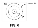
図6は、多数の例示的な実施態様に従った、体積変化基板の中心領域の周りで同心状に異なる厚さを有する体積変化基板600の頂面図である。体積変化基板600の厚さは、体積変化基板600に取り付けられる(例えば、結合される或いは接着される)画像センサチップ(図6に示されていない)の曲げの形状に影響を与える特別な仕方において異なってよい。等値線602(iso-lines)は一定の厚さの線を示す。隣接する等値線602の間の間隔は異なってよく、変化する厚さを示す。例えば、互いに比較的近く離間する等値線602は、厚さが(Rによって示す)半径方向において比較的短い距離に亘って素早く変化することを示す。同心状の等値線602は、体積変化基板600の厚さが径方向において対称的に異なることを示す。従って、加工業者は、画像センサチップを球面の形状(例えば、等しい間隔を有する同心状の等値線)、非球面又は放物線状の形状(例えば、等しくない間隔を有する同心状の等値線)、又はより複雑な形状(例えば、特異な間隔を有する非同心状の等値線)に形成するために、そのような方法において異なる厚さを有する体積変化基板600を用いてよい。
FIG. 6 is a top view of a
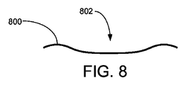
図7及び8は、様々な例示的な実施態様に従った、湾曲した画像センサチップの感光部分の形状を例示する断面図である。図7では、湾曲した画像センサチップ702の感光部分700が、球面又は非球面の形状を有する。そのような形状は、反射地点を有さない。感光部分700は、凹面である。他方、図8に例示するように、湾曲した画像センサチップ802の感光部分800は、1つ又はそれよりも多くの反射地点を含む複雑な形状を有する。感光部分800の部分は、球面又は非球面の形状を含んでよい。そのような複雑な形状は、多数の光学系において有用なことがある。上述のような体積変化基板を、適用される力及び/又はトルクとの組み合わせにおいて設計して、感光部分800の複雑な形状をもたらしてよい。
7 and 8 are cross-sectional views illustrating the shape of the photosensitive portion of a curved image sensor chip, according to various exemplary embodiments. In FIG. 7, the
図9は、様々な例示的な実施態様に従った、体積変化基板902に取り付けられる、湾曲した画像センサチップ900の湾曲を例示する、断面図である。体積変化基板に結合される湾曲した画像センサチップの組み合わせは、引き続き光学系内に組み込まれてよい、スタンドアローンの光学デバイスを含んでよい。そのような光学系の光学軸904が、画像センサチップ900に関して示されている。体積変化基板の寸法及び体積は、光学系にとって或いは膨張剤のない場合に典型的である環境条件(例えば、室温、大気圧)の下で、(例えば、数十年以上)一定なままであってよい。例えば、体積変化基板902の体積膨張をもたらす水素化反応は発熱性であってよい。従って、体積膨張した基板は、比較的化学的及び物理的に安定的である。
FIG. 9 is a cross-sectional view illustrating the curvature of a curved
少なくとも部分的に、画像センサチップ900の湾曲した形状に基づく、画像センサチップ900の焦点距離は、画像センサチップ900が光学系内に組み込まれるときに、有意な要因であることがある。画像センサチップ900の形状が実質的に球面であるとき、画像センサチップ900の書店距離は、画像センサチップ900の曲率半径Rの逆と少なくとも略等しい。画像センサチップ900が非球面の形状を有するならば、画像センサチップ900の曲率半径は、光学軸904からの距離に応じて変化する。画像センサチップ900を含む光学系は、そのような可変な曲率半径に適合するように設計されてよい。
The focal length of the
図10は、様々な例示的な実施態様に従った、画像センサモジュール1002と、レンズアセンブリ1004とを含む、光学系1000の断面図である。具体的には、画像センサモジュール1002は、湾曲した画像センサチップ1006及び体積変化基板を含む。湾曲した画像センサチップ1006は、感光部分1010を含む。湾曲した画像センサチップ1006及び体積変化基板1008は、それぞれ、図3に例示した湾曲した画像センサチップ302及び体積変化基板304と類似又は同一であってよい。幾つかの実施態様において、体積変化基板1008は、湾曲した画像センサチップ1006の湾曲した形状を維持するよう十分に剛的であってよい。
FIG. 10 is a cross-sectional view of an
湾曲した画像センサチップ1006(又は感光部分1010)は、焦点距離を生じさせる形状を有してよい。そのような焦点距離は、画像センサモジュール1002を光学系1000内に配置するときに考慮されてよい。具体的には、レンズアセンブリ1004は、光1012を受光し、光に対して光学的に影響を及ぼし、且つ湾曲した画像センサチップ1006の上に画像を集束させる光出力1014を生成するように、設計されてよく、湾曲した画像センサチップ1006は、レンズアセンブリ1004からある距離1016にあってよい。距離1016は、湾曲した画像センサチップ1006の焦点距離と少なくとも略等しくてよい。幾つかの実施態様において、湾曲した画像センサチップ1006の焦点距離の逆は、湾曲した画像繊細チップ1006の曲率半径と少なくとも略等しくてよい。レンズアセンブリ1004及び画像センサモジュール1002は、光学軸1018に沿って整列させられてよい。
The curved image sensor chip 1006 (or photosensitive portion 1010) may have a shape that produces a focal length. Such focal length may be considered when placing the
図11は、幾つかの例示的な実施態様に従った、画像センサチップを曲げるプロセス1100を例示するフロー図である。例えば、そのような画像センサチップは、図3に示す画像センサチップ302と同一又は類似であってよい。プロセス1100は、図3乃至5に描写するプロセスと類似又は同一であってよく、加工業者によって行われてよい。ブロック1102で、加工業者は、画像センサチップの第1の表面の上に基板を配置してよく、画像センサチップの第1の表面は、画像センサチップの第2の表面の反対側にあり、画像センサチップの第2の表面は、受光する光に応答して電気信号を生成する光センサを含む。ブロック1104で、加工業者は、画像センサチップの上に力を加えて湾曲した画像センサチップをもたらすよう、基板の体積を変更してよい。
FIG. 11 is a flow diagram illustrating a
(例示的な節)
A.画像センサチップの第1の表面の上に基板を配置するステップであって、前記第1の表面は、画像センサチップの第2の表面の反対側にあり、画像センサチップの第2の表面は、受光する光に応答して電気信号を生成する光センサを含む、ステップと、画像センサチップの上に力を加えて湾曲した画像センサチップをもたらすよう、基板の体積を変更するステップとを含む、方法。
(Example section)
A. Placing a substrate on a first surface of an image sensor chip, wherein the first surface is opposite the second surface of the image sensor chip, and the second surface of the image sensor chip is Including a photosensor that generates an electrical signal in response to received light, and applying a force on the image sensor chip to change the volume of the substrate to provide a curved image sensor chip. ,Method.
B.湾曲した画像センサチップの前記第2の側面は、凹球面又は非球面の形状を有する、段落Aに記載する方法。 B. The method of paragraph A, wherein the second side of the curved image sensor chip has a concave spherical or aspherical shape.
C.画像センサチップの第1の表面の上に基板を配置するステップは、インターフェース層を用いて画像センサチップの第1の表面を基板に連結するステップを含む、段落A及びBのうちのいずれかに記載する方法。 C. Placing the substrate on the first surface of the image sensor chip includes coupling the first surface of the image sensor chip to the substrate using an interface layer, in any of paragraphs A and B. How to describe.
D.基板は、金属合金を含み、基板の体積を変更するステップは、基板を水素に晒して、基板が水素を吸収するのを許容するステップを含む、段落A乃至Cのうちのいずれかに記載する方法。 D. The substrate includes a metal alloy, and changing the volume of the substrate includes exposing the substrate to hydrogen and allowing the substrate to absorb hydrogen, according to any of paragraphs A-C. Method.
E.基板は、金属合金を含み、基板の体積を変更するステップは、基板の少なくとも部分に電流を適用して、酸素化反応を行うステップを含む、段落A乃至Cのうちのいずれかに記載する方法。 E. The method of any of paragraphs A-C, wherein the substrate includes a metal alloy and the step of changing the volume of the substrate includes applying an electric current to at least a portion of the substrate to perform an oxygenation reaction. .
F.金属合金は、アルミニウム又はチタンを含む、段落A乃至Dのうちのいずれかに記載する方法。 F. The method according to any one of paragraphs A to D, wherein the metal alloy comprises aluminum or titanium.
G.基板の体積を変更するステップは、リチオ化プロセスにおいて基板をリチウム基の化学薬品に晒すステップを含む、段落A乃至Cのうちのいずれかに記載する方法。 G. The method of any of paragraphs A-C, wherein altering the volume of the substrate comprises exposing the substrate to a lithium-based chemical in a lithiation process.
H.基板は、ポリマ又はエラストマを含み、基板の体積を変更するステップは、水化プロセス又は溶媒和プロセスにおいて基板を1つ又はそれよりも多くの化学薬品に晒すステップを含む、段落A乃至Cのうちのいずれかに記載する方法。 H. Of paragraphs A-C, wherein the substrate comprises a polymer or elastomer, and the step of changing the volume of the substrate comprises exposing the substrate to one or more chemicals in a hydration or solvation process. The method described in any one of.
I.基板の体積を変更するステップは、制御された温度、圧力、又は電圧を前記基板の特定の部分に適用するステップを含む、段落A乃至Cのうちのいずれかに記載する方法。 I. The method of any of paragraphs A through C, wherein changing the volume of the substrate comprises applying a controlled temperature, pressure, or voltage to a particular portion of the substrate.
J.基板の体積を変更するステップ前に、基板は、第1の厚さプロファイルを有し、基板の体積を変更するステップの後に、基板は、第1の厚さプロファイルと異なる第2の厚さプロファイルを有する、段落A乃至Cのうちのいずれかに記載する方法。 J. et al. Before the step of changing the volume of the substrate, the substrate has a first thickness profile, and after the step of changing the volume of the substrate, the substrate has a second thickness profile that is different from the first thickness profile. The method according to any one of paragraphs A to C, comprising:
K.画像センサの前記第2の表面に隣接して形成型を配置するステップを更に含む、段落A乃至Cのうちのいずれかに記載する方法。 K. The method of any of paragraphs A through C, further comprising positioning a mold adjacent to the second surface of the image sensor.
L.第1の側面と、第1の側面の反対側にある第2の側面とを有し、第2の側面は、受光する光に応答して電気信号を生成する光センサを含む、湾曲した画像センサチップと、湾曲した画像センサチップの第1の側面を覆い、水素化金属を含む、基板とを含む、装置。 L. A curved image having a first side and a second side opposite to the first side, the second side including a photosensor that generates an electrical signal in response to the received light An apparatus comprising: a sensor chip; and a substrate covering a first side of the curved image sensor chip and comprising a metal hydride.
M.湾曲した画像センサチップの前記第2の側面は、凹球面又は非球面の形状を有する、段落Lに記載する装置。 M.M. The apparatus of paragraph L, wherein the second side surface of the curved image sensor chip has a concave spherical or aspherical shape.
N.水素化金属は、水素化チタン又は水素化バナジウムを含む、段落L及びMのうちのいずれかに記載する装置。 N. The apparatus according to any of paragraphs L and M, wherein the metal hydride comprises titanium hydride or vanadium hydride.
O.基板を湾曲した画像センサチップの第2の側面に連結するインターフェース層を更に含む、段落L乃至Nのうちのいずれかに記載する装置。 O. The apparatus of any of paragraphs L through N, further comprising an interface layer connecting the substrate to the second side of the curved image sensor chip.
P.湾曲した画像センサチップは、湾曲した画像センサチップの第2の側面の逆の焦点距離と少なくとも略等しい曲率半径を有する、段落L乃至Oのうちのいずれかに記載する装置。 P. The apparatus according to any of paragraphs L through O, wherein the curved image sensor chip has a radius of curvature that is at least approximately equal to the opposite focal length of the second side of the curved image sensor chip.
Q.1つ若しくはそれよりも多くのレンズ又はミラーと、第1の側面と、第1の側面の反対側にある第2の側面とを有し、第2の側面は、1つ若しくはそれよりも多くのレンズ又はミラーから受光する光に応答して電気信号を生成する光センサを含む、湾曲した画像センサチップと、湾曲した画像センサチップの第2の側面を覆い、水素化金属を含む、基板とを含む、システム。 Q. Having one or more lenses or mirrors, a first side and a second side opposite the first side, wherein the second side is one or more A curved image sensor chip that includes an optical sensor that generates an electrical signal in response to light received from the lens or mirror of the lens, and a substrate that covers a second side of the curved image sensor chip and includes a metal hydride. Including the system.
R.基板は、基板による1つ若しくはそれよりも多くの膨張させる化学薬品の吸収を少なくとも部分的に妨げるマスク領域を含む、段落Qに記載するシステム。 R. The system of paragraph Q, wherein the substrate includes a mask region that at least partially impedes absorption of one or more inflating chemicals by the substrate.
S.湾曲した画像センサチップは、湾曲した画像センサチップの第2の側面の逆の焦点距離と少なくとも略等しい曲率半径を有する、段落Q及びRのうちのいずれかに記載するシステム。 S. The system of any of paragraphs Q and R, wherein the curved image sensor chip has a radius of curvature that is at least approximately equal to the opposite focal length of the second side of the curved image sensor chip.
T.画像センサチップは、シリコン又はゲルマニウムを含む、段落Q乃至Sのうちのいずれかに記載するシステム。 T. T. The system of any of paragraphs Q through S, wherein the image sensor chip comprises silicon or germanium.
(結論)
構造的な構成及び/又は方法論的な行為に特異な言語において主題を記載したが、付属の請求項において定められる主題は記載する特異な構成または行為に必ずしも限定されないことが理解されなければならない。むしろ特異の構成及びステップは、請求項を実施する例示的な形態として開示される。
(Conclusion)
Although the subject matter has been described in language specific to structural arrangements and / or methodological acts, it is to be understood that the subject matter defined in the appended claims is not necessarily limited to the specific configurations or acts described. Rather, the specific configurations and steps are disclosed as exemplary forms of implementing the claims.
上述の方法及びプロセスの全ては、1つ又はそれよりも多くの汎用コンピュータ又はプロセッサによって実行されるソフトウェアコードモジュールを介して完全に自動化されて具現されてよい。コードモジュールは、任意の種類のコンピュータ可読媒体、コンピュータ記憶媒体、又は他のコンピュータ記憶デバイス内に格納されてよい。方法の一部又は全部は、代替的に、例えば、量子コンピュータ又は量子アニーリング装置(annealer)のような、特殊なコンピュータハードウェアにおいて具現されてよい。 All of the methods and processes described above may be implemented fully automated via software code modules executed by one or more general purpose computers or processors. A code module may be stored in any type of computer readable media, computer storage media, or other computer storage devices. Some or all of the methods may alternatively be embodied in specialized computer hardware, such as, for example, a quantum computer or a quantum annealing device.
とりわけ、「できる」(“can”)、「できた」(“could”)、「〜してよい」(“may”)又は「〜ことがある」(“may”)のような、条件的な言語は、特段の断りのない限り、特定の実施例が特定の構成、要素、及び/又はステップを含むが、他の実施例がそれらを含まないことを伝える文脈内で理解される。よって、そのような条件的な言語は、特定の構成、要素、及び/又はステップが、1つ又はそれよりも多くの実施例のためにいずれにしても必要とされること、或いは、1つ又はそれよりも多くの実施例が、使用者入力又は使用者プロンプトを伴って或いは伴わないで、特定の構成、要素、及び/又はステップがいずれかの特定の実施例に含まれるか又はいずれかの特定の実施例において行われるべきかを決定する論理を必ず含むことを暗示することを、概して意図しない。 In particular, conditional such as “can”, “could”, “may” or “may” Unless otherwise noted, certain languages are understood within the context that a particular embodiment includes a particular configuration, element, and / or step, but that other embodiments do not. Thus, such conditional language is such that a particular configuration, element, and / or step is required anyway for one or more embodiments, or one Or more than one embodiment, with or without user input or user prompt, with particular configurations, elements, and / or steps included in any particular embodiment, or any It is generally not intended to imply that it necessarily includes logic to determine what should be done in this particular embodiment.
「X、Y、又はZのうちの少なくとも1つ」のような接続言語は、特段の断りのない限り、ある品目、用語等が、X、Y、Z、又はそれらの組み合わせのいずれかであることを伝えるものと理解されるべきである。 A connection language such as “at least one of X, Y, or Z” is an item, term, etc. that is either X, Y, Z, or a combination thereof, unless otherwise specified. It should be understood as a communication.
本明細書中で記載する或いは添付の図面中に描写するフロー図中のあらゆる慣例的な記述、要素、又はブロックは、慣例における具体的な論理機能又は要素を実施するための1つ又はそれよりも多くの実行可能な指令を含むコードの部分、セグメント、又はモジュールを潜在的に表すものとして理解されなければならない。代替的な実施が、本明細書中に記載する実施例の範囲内に含められ、それらの要素又は機能は、当業者によって理解されるものとして含められる機能性に依存して、実質的に同時又は逆の順序を含んで、図示され或いは議論されたものから削除され或いはバラバラの順序で実行されてよい。 Any conventional descriptions, elements, or blocks in the flow diagrams set forth herein or depicted in the accompanying drawings may be used to implement one or more specific logic functions or elements in the practice. Must also be understood as potentially representing a portion, segment, or module of code that contains many executable instructions. Alternative implementations are included within the scope of the embodiments described herein, and their elements or functions are substantially simultaneous, depending on the functionality included as understood by those skilled in the art. Or it may be deleted from what is shown or discussed, including the reverse order, or performed in a disjoint order.
多くの変形及び修正が上述の実施例に対して行われてよく、それらの要素は、他の許容される実施例の中にあるものとして理解されるべきであることが強調されなければならない。全てのそのような修正及び変形は、この開示の範囲内で本明細書中に含まれ且つ後続の請求項によって保護されることが意図される。 It should be emphasized that many variations and modifications may be made to the above-described embodiments, and that those elements should be understood as being within other acceptable embodiments. All such modifications and variations are intended to be included herein within the scope of this disclosure and protected by the following claims.
Claims (15)
前記画像センサチップの上に力を加えて湾曲した画像センサチップをもたらすよう、前記基板の体積を変更するステップとを含む、
方法。 Disposing a substrate on a first surface of an image sensor chip, wherein the first surface is opposite to a second surface of the image sensor chip and the second of the image sensor chip; The surface includes a photosensor that generates an electrical signal in response to the received light; and
Changing the volume of the substrate to apply a force on the image sensor chip to provide a curved image sensor chip;
Method.
該湾曲した画像センサチップの前記第1の側面を覆い、水素化金属を含む、基板とを含む、
装置。 A curved surface having a first side and a second side opposite to the first side, the second side including an optical sensor that generates an electrical signal in response to received light Image sensor chip
Covering the first side of the curved image sensor chip and including a metal hydride,
apparatus.
第1の側面と、該第1の側面の反対側にある第2の側面とを有し、該第2の側面は、前記1つ若しくはそれよりも多くのレンズ又はミラーから受光する光に応答して電気信号を生成する光センサを含む、湾曲した画像センサチップと、
該湾曲した画像センサチップの前記第2の側面を覆い、水素化金属を含む、基板とを含む、
システム。 One or more lenses or mirrors;
A first side and a second side opposite the first side, the second side being responsive to light received from the one or more lenses or mirrors A curved image sensor chip including an optical sensor that generates an electrical signal
Covering the second side of the curved image sensor chip and including a metal hydride,
system.
Applications Claiming Priority (3)
| Application Number | Priority Date | Filing Date | Title |
|---|---|---|---|
| US14/491,903 US9570488B2 (en) | 2014-09-19 | 2014-09-19 | Image sensor bending by induced substrate swelling |
| US14/491,903 | 2014-09-19 | ||
| PCT/US2015/049277 WO2016044040A1 (en) | 2014-09-19 | 2015-09-10 | Image sensor bending by induced substrate swelling |
Publications (1)
| Publication Number | Publication Date |
|---|---|
| JP2017531319A true JP2017531319A (en) | 2017-10-19 |
Family
ID=54199296
Family Applications (1)
| Application Number | Title | Priority Date | Filing Date |
|---|---|---|---|
| JP2017515090A Pending JP2017531319A (en) | 2014-09-19 | 2015-09-10 | Image sensor bending by induced substrate expansion |
Country Status (16)
| Country | Link |
|---|---|
| US (2) | US9570488B2 (en) |
| EP (1) | EP3195360B1 (en) |
| JP (1) | JP2017531319A (en) |
| KR (1) | KR102444392B1 (en) |
| CN (1) | CN107078142B (en) |
| AU (1) | AU2015318206A1 (en) |
| BR (1) | BR112017003628A2 (en) |
| CA (1) | CA2961181A1 (en) |
| CL (1) | CL2017000648A1 (en) |
| CO (1) | CO2017002554A2 (en) |
| IL (1) | IL250482A0 (en) |
| MX (1) | MX2017003531A (en) |
| PH (1) | PH12017500248A1 (en) |
| RU (1) | RU2017108847A (en) |
| SG (1) | SG11201701827YA (en) |
| WO (1) | WO2016044040A1 (en) |
Families Citing this family (19)
| Publication number | Priority date | Publication date | Assignee | Title |
|---|---|---|---|---|
| US9570488B2 (en) | 2014-09-19 | 2017-02-14 | Microsoft Technology Licensing, Llc | Image sensor bending by induced substrate swelling |
| US10373995B2 (en) | 2014-09-19 | 2019-08-06 | Microsoft Technology Licensing, Llc | Image sensor bending using tension |
| CN104486555B (en) * | 2014-10-28 | 2019-02-12 | 北京智谷睿拓技术服务有限公司 | Image Acquisition control method and device |
| US11128786B2 (en) * | 2014-11-21 | 2021-09-21 | Apple Inc. | Bending a circuit-bearing die |
| JP6463159B2 (en) * | 2015-02-05 | 2019-01-30 | キヤノン株式会社 | IMAGING DEVICE, ITS CONTROL METHOD, PROGRAM, AND STORAGE MEDIUM |
| US10304900B2 (en) | 2015-04-02 | 2019-05-28 | Microsoft Technology Licensing, Llc | Bending semiconductor chip in molds having radially varying curvature |
| US9870927B2 (en) | 2015-04-02 | 2018-01-16 | Microsoft Technology Licensing, Llc | Free-edge semiconductor chip bending |
| US9893058B2 (en) * | 2015-09-17 | 2018-02-13 | Semiconductor Components Industries, Llc | Method of manufacturing a semiconductor device having reduced on-state resistance and structure |
| KR102072666B1 (en) * | 2016-01-26 | 2020-02-03 | 한국전자통신연구원 | Optical imaging device |
| US10062727B2 (en) | 2016-09-09 | 2018-08-28 | Microsoft Technology Licensing, Llc | Strain relieving die for curved image sensors |
| US10361235B2 (en) * | 2016-11-23 | 2019-07-23 | Industrial Technology Research Institute | Image sensor |
| FR3061990B1 (en) * | 2017-01-18 | 2019-04-19 | Commissariat A L'energie Atomique Et Aux Energies Alternatives | METHOD FOR COLLECTIVELY PRODUCING CURVED ELECTRONIC CIRCUITS |
| FR3073322B1 (en) * | 2017-11-07 | 2021-12-03 | Commissariat Energie Atomique | PROCESS FOR MAKING AT LEAST ONE CURVED ELECTRONIC CIRCUIT |
| CN107959781B (en) * | 2017-12-11 | 2020-07-31 | 信利光电股份有限公司 | Camera module and adjustment control method thereof |
| US11848349B1 (en) * | 2018-06-21 | 2023-12-19 | Hrl Laboratories, Llc | Curved semiconductor and method of forming the same |
| US10418408B1 (en) * | 2018-06-22 | 2019-09-17 | Omnivision Technologies, Inc. | Curved image sensor using thermal plastic substrate material |
| TWI660493B (en) * | 2018-12-06 | 2019-05-21 | 財團法人工業技術研究院 | Image sensor and manufacturing method thereof |
| CN116413885A (en) * | 2019-09-24 | 2023-07-11 | 核心光电有限公司 | Thin pop-up camera and lens for such camera |
| US11862653B2 (en) | 2020-04-02 | 2024-01-02 | Hrl Laboratories, Llc | Curved imaging sensor package with architected substrate |
Family Cites Families (55)
| Publication number | Priority date | Publication date | Assignee | Title |
|---|---|---|---|---|
| EP0576144B1 (en) | 1992-05-22 | 1998-08-05 | Matsushita Electronics Corporation | Solid state image sensor and manufacturing method thereof |
| US5349443A (en) | 1992-11-25 | 1994-09-20 | Polaroid Corporation | Flexible transducers for photon tunneling microscopes and methods for making and using same |
| JP2809215B2 (en) | 1996-09-26 | 1998-10-08 | 日本電気株式会社 | Solid-state imaging camera |
| JPH1174164A (en) | 1997-08-27 | 1999-03-16 | Canon Inc | Wafer-processing device, wafer support device, wafer-processing method, and manufacture of wafer |
| US6255025B1 (en) * | 1998-07-13 | 2001-07-03 | Fuji Xerox Co., Ltd. | Filter and process for producing same |
| US6312959B1 (en) | 1999-03-30 | 2001-11-06 | U.T. Battelle, Llc | Method using photo-induced and thermal bending of MEMS sensors |
| US6706448B1 (en) * | 1999-08-30 | 2004-03-16 | Georgia Tech Research Corp. | Method and apparatus for lithiating alloys |
| JP4604307B2 (en) | 2000-01-27 | 2011-01-05 | ソニー株式会社 | Imaging apparatus, method for manufacturing the same, and camera system |
| US9314339B2 (en) * | 2000-03-27 | 2016-04-19 | Formae, Inc. | Implants for replacing cartilage, with negatively-charged hydrogel surfaces and flexible matrix reinforcement |
| TWI313059B (en) * | 2000-12-08 | 2009-08-01 | Sony Corporatio | |
| DE10122324A1 (en) | 2001-05-08 | 2002-11-14 | Philips Corp Intellectual Pty | Flexible integrated monolithic circuit |
| US6791072B1 (en) | 2002-05-22 | 2004-09-14 | National Semiconductor Corporation | Method and apparatus for forming curved image sensor module |
| US6881491B2 (en) * | 2003-05-16 | 2005-04-19 | Alcoa Inc. | Protective fluoride coatings for aluminum alloy articles |
| JP4705748B2 (en) * | 2003-05-30 | 2011-06-22 | ルネサスエレクトロニクス株式会社 | Manufacturing method of semiconductor device |
| JP2005278133A (en) * | 2003-07-03 | 2005-10-06 | Fuji Photo Film Co Ltd | Solid state imaging device and optical device |
| US20050035514A1 (en) | 2003-08-11 | 2005-02-17 | Supercritical Systems, Inc. | Vacuum chuck apparatus and method for holding a wafer during high pressure processing |
| US7397066B2 (en) | 2004-08-19 | 2008-07-08 | Micron Technology, Inc. | Microelectronic imagers with curved image sensors and methods for manufacturing microelectronic imagers |
| US7432596B1 (en) | 2004-10-12 | 2008-10-07 | Energy Innovations, Inc. | Apparatus and method for bonding silicon wafer to conductive substrate |
| US7190039B2 (en) * | 2005-02-18 | 2007-03-13 | Micron Technology, Inc. | Microelectronic imagers with shaped image sensors and methods for manufacturing microelectronic imagers |
| US7683303B2 (en) | 2006-01-17 | 2010-03-23 | Sri International | Nanoscale volumetric imaging device having at least one microscale device for electrically coupling at least one addressable array to a data processing means |
| US7507944B1 (en) | 2006-06-27 | 2009-03-24 | Cypress Semiconductor Corporation | Non-planar packaging of image sensor |
| JP2008092532A (en) | 2006-10-05 | 2008-04-17 | Matsushita Electric Ind Co Ltd | Imaging apparatus, manufacturing method therefor and mobile phone unit |
| US7733397B2 (en) | 2006-12-22 | 2010-06-08 | Palo Alto Research Center Incorporated | Sensor surface with 3D curvature formed by electronics on a continuous 2D flexible substrate |
| US7742090B2 (en) | 2006-12-22 | 2010-06-22 | Palo Alto Research Center Incorporated | Flexible segmented image sensor |
| JP2009049499A (en) | 2007-08-14 | 2009-03-05 | Fujifilm Corp | Method for mounting semiconductor chip, and semiconductor device |
| KR101378418B1 (en) | 2007-11-01 | 2014-03-27 | 삼성전자주식회사 | image sensor module and fabrication method thereof |
| US8077235B2 (en) | 2008-01-22 | 2011-12-13 | Palo Alto Research Center Incorporated | Addressing of a three-dimensional, curved sensor or display back plane |
| US8372726B2 (en) | 2008-10-07 | 2013-02-12 | Mc10, Inc. | Methods and applications of non-planar imaging arrays |
| KR101567067B1 (en) | 2008-12-02 | 2015-11-06 | 엘지이노텍 주식회사 | Camera Module |
| US8248499B2 (en) | 2009-02-23 | 2012-08-21 | Gary Edwin Sutton | Curvilinear sensor system |
| US20120159996A1 (en) * | 2010-12-28 | 2012-06-28 | Gary Edwin Sutton | Curved sensor formed from silicon fibers |
| US8836805B2 (en) | 2012-07-17 | 2014-09-16 | Gary Edwin Sutton | Curved sensor system |
| CN102413999A (en) | 2009-02-27 | 2012-04-11 | Hoya株式会社 | Method of producing mold for lens and method of producing eyeglass lens |
| GB0915473D0 (en) | 2009-09-07 | 2009-10-07 | St Microelectronics Res & Dev | Improvements in or relating to CMOS sensors |
| WO2011059766A1 (en) * | 2009-10-29 | 2011-05-19 | The Board Of Trustees Of The Leland Stanford Junior University | Devices, systems and methods for advanced rechargeable batteries |
| EP2388987A1 (en) | 2010-05-19 | 2011-11-23 | Thomson Licensing | Camera with volumetric sensor chip |
| JP5724322B2 (en) | 2010-11-24 | 2015-05-27 | ソニー株式会社 | Method for manufacturing solid-state imaging device |
| WO2012097163A1 (en) | 2011-01-14 | 2012-07-19 | The Board Of Trustees Of The University Of Illinois | Optical component array having adjustable curvature |
| US9228822B2 (en) | 2011-01-24 | 2016-01-05 | President And Fellows Of Harvard College | Non-differential elastomer curvature sensor |
| US8878116B2 (en) * | 2011-02-28 | 2014-11-04 | Sony Corporation | Method of manufacturing solid-state imaging element, solid-state imaging element and electronic apparatus |
| JP5720304B2 (en) | 2011-02-28 | 2015-05-20 | ソニー株式会社 | Solid-state imaging device and electronic device |
| JP5658189B2 (en) * | 2011-03-21 | 2015-01-21 | ゲイリー・エドウィン・サットン | Mobile communication device having a curved sensor camera, curved sensor camera having a movable optical unit, and curved sensor made of silicon fiber |
| JP2012249003A (en) | 2011-05-26 | 2012-12-13 | Toshiba Corp | Solid-state imaging device, manufacturing method of the same, and camera module |
| US20150120661A1 (en) | 2012-04-04 | 2015-04-30 | Scribble Technologies Inc. | System and Method for Generating Digital Content |
| FR2989518A1 (en) | 2012-04-13 | 2013-10-18 | St Microelectronics Crolles 2 | Method for manufacturing integrated image sensor, involves forming pixels at end of columns, and deforming structure such that another end of each of columns is brought closer or separated to form surface in shape of polyhedral cap |
| FR2989519A1 (en) | 2012-04-13 | 2013-10-18 | St Microelectronics Crolles 2 | METHOD OF MANUFACTURING A CURVED SURFACE IMAGE SENSOR |
| US10334181B2 (en) | 2012-08-20 | 2019-06-25 | Microsoft Technology Licensing, Llc | Dynamically curved sensor for optical zoom lens |
| JP6135109B2 (en) | 2012-12-07 | 2017-05-31 | ソニー株式会社 | Solid-state imaging device, manufacturing method of solid-state imaging device, and electronic apparatus |
| JP2015070159A (en) | 2013-09-30 | 2015-04-13 | ソニー株式会社 | Solid state image sensor and manufacturing method therefor, and electronic apparatus |
| KR101557942B1 (en) | 2014-01-08 | 2015-10-12 | 주식회사 루멘스 | Light emitting device package and its manufacturing method |
| US9551856B2 (en) | 2014-05-19 | 2017-01-24 | Google Inc. | MEMS-released curved image sensor |
| US9570488B2 (en) | 2014-09-19 | 2017-02-14 | Microsoft Technology Licensing, Llc | Image sensor bending by induced substrate swelling |
| US10373995B2 (en) | 2014-09-19 | 2019-08-06 | Microsoft Technology Licensing, Llc | Image sensor bending using tension |
| US9349763B1 (en) | 2015-02-10 | 2016-05-24 | Omnivision Technologies, Inc. | Curved image sensor systems and methods for manufacturing the same |
| US9998643B2 (en) | 2015-03-24 | 2018-06-12 | Semiconductor Components Industries, Llc | Methods of forming curved image sensors |
-
2014
- 2014-09-19 US US14/491,903 patent/US9570488B2/en active Active
-
2015
- 2015-09-10 RU RU2017108847A patent/RU2017108847A/en not_active Application Discontinuation
- 2015-09-10 CN CN201580050442.XA patent/CN107078142B/en active Active
- 2015-09-10 BR BR112017003628A patent/BR112017003628A2/en not_active Application Discontinuation
- 2015-09-10 AU AU2015318206A patent/AU2015318206A1/en not_active Abandoned
- 2015-09-10 MX MX2017003531A patent/MX2017003531A/en unknown
- 2015-09-10 CA CA2961181A patent/CA2961181A1/en not_active Abandoned
- 2015-09-10 SG SG11201701827YA patent/SG11201701827YA/en unknown
- 2015-09-10 JP JP2017515090A patent/JP2017531319A/en active Pending
- 2015-09-10 EP EP15770998.1A patent/EP3195360B1/en active Active
- 2015-09-10 WO PCT/US2015/049277 patent/WO2016044040A1/en active Application Filing
- 2015-09-10 KR KR1020177010521A patent/KR102444392B1/en active IP Right Grant
-
2017
- 2017-01-04 US US15/398,266 patent/US9859314B2/en active Active
- 2017-02-07 IL IL250482A patent/IL250482A0/en unknown
- 2017-02-09 PH PH12017500248A patent/PH12017500248A1/en unknown
- 2017-03-16 CL CL2017000648A patent/CL2017000648A1/en unknown
- 2017-03-17 CO CONC2017/0002554A patent/CO2017002554A2/en unknown
Also Published As
| Publication number | Publication date |
|---|---|
| US9859314B2 (en) | 2018-01-02 |
| AU2015318206A1 (en) | 2017-03-16 |
| KR102444392B1 (en) | 2022-09-16 |
| IL250482A0 (en) | 2017-03-30 |
| CN107078142A (en) | 2017-08-18 |
| SG11201701827YA (en) | 2017-04-27 |
| US9570488B2 (en) | 2017-02-14 |
| WO2016044040A1 (en) | 2016-03-24 |
| BR112017003628A2 (en) | 2017-12-12 |
| CN107078142B (en) | 2020-08-18 |
| EP3195360A1 (en) | 2017-07-26 |
| KR20170056689A (en) | 2017-05-23 |
| RU2017108847A (en) | 2018-09-17 |
| MX2017003531A (en) | 2017-06-21 |
| US20170117311A1 (en) | 2017-04-27 |
| EP3195360B1 (en) | 2019-05-01 |
| US20160086987A1 (en) | 2016-03-24 |
| CA2961181A1 (en) | 2016-03-24 |
| CO2017002554A2 (en) | 2017-06-20 |
| PH12017500248A1 (en) | 2017-07-03 |
| CL2017000648A1 (en) | 2017-11-17 |
Similar Documents
| Publication | Publication Date | Title |
|---|---|---|
| JP2017531319A (en) | Image sensor bending by induced substrate expansion | |
| KR102466067B1 (en) | Image sensor bending using tension | |
| Guenter et al. | Highly curved image sensors: a practical approach for improved optical performance | |
| US10062727B2 (en) | Strain relieving die for curved image sensors | |
| CN107431079B (en) | Free edge semiconductor chip bending | |
| EP3278362B1 (en) | Bending semiconductor chip in molds having radially varying curvature | |
| WO2012097163A1 (en) | Optical component array having adjustable curvature | |
| Dumas et al. | Infrared camera based on a curved retina | |
| Chambion et al. | Tunable curvature of large visible CMOS image sensors: Towards new optical functions and system miniaturization | |
| Hugot et al. | Flexible focal plane arrays for UVOIR wide field instrumentation | |
| Chambion et al. | Curved sensors for compact high-resolution wide-field designs: prototype demonstration and optical characterization | |
| Gaschet et al. | Curved sensors for compact high-resolution wide field designs | |
| Tekaya et al. | Mechanical behavior of flexible silicon devices curved in spherical configurations | |
| Shaw et al. | A study of the sensor shape of a hemispherical electronic eye variable focus camera lens |