JP2017520168A - Feedback reception path using RF filter - Google Patents
Feedback reception path using RF filter Download PDFInfo
- Publication number
- JP2017520168A JP2017520168A JP2016569647A JP2016569647A JP2017520168A JP 2017520168 A JP2017520168 A JP 2017520168A JP 2016569647 A JP2016569647 A JP 2016569647A JP 2016569647 A JP2016569647 A JP 2016569647A JP 2017520168 A JP2017520168 A JP 2017520168A
- Authority
- JP
- Japan
- Prior art keywords
- filter
- elliptical
- node
- signal
- notch
- Prior art date
- Legal status (The legal status is an assumption and is not a legal conclusion. Google has not performed a legal analysis and makes no representation as to the accuracy of the status listed.)
- Ceased
Links
Images
Classifications
-
- H—ELECTRICITY
- H04—ELECTRIC COMMUNICATION TECHNIQUE
- H04B—TRANSMISSION
- H04B1/00—Details of transmission systems, not covered by a single one of groups H04B3/00 - H04B13/00; Details of transmission systems not characterised by the medium used for transmission
- H04B1/06—Receivers
- H04B1/10—Means associated with receiver for limiting or suppressing noise or interference
- H04B1/12—Neutralising, balancing, or compensation arrangements
-
- H—ELECTRICITY
- H04—ELECTRIC COMMUNICATION TECHNIQUE
- H04B—TRANSMISSION
- H04B1/00—Details of transmission systems, not covered by a single one of groups H04B3/00 - H04B13/00; Details of transmission systems not characterised by the medium used for transmission
- H04B1/02—Transmitters
- H04B1/04—Circuits
- H04B1/0475—Circuits with means for limiting noise, interference or distortion
-
- H—ELECTRICITY
- H04—ELECTRIC COMMUNICATION TECHNIQUE
- H04B—TRANSMISSION
- H04B15/00—Suppression or limitation of noise or interference
-
- H—ELECTRICITY
- H04—ELECTRIC COMMUNICATION TECHNIQUE
- H04B—TRANSMISSION
- H04B1/00—Details of transmission systems, not covered by a single one of groups H04B3/00 - H04B13/00; Details of transmission systems not characterised by the medium used for transmission
- H04B1/02—Transmitters
- H04B1/04—Circuits
- H04B2001/0408—Circuits with power amplifiers
- H04B2001/0416—Circuits with power amplifiers having gain or transmission power control
Abstract
装置は、楕円インダクタンスキャパシタンス(LC)フィルタと、楕円LCフィルタに直列に結合された抵抗容量性(RC)ノッチフィルタとを含む。楕円LCフィルタおよびRCノッチフィルタは、フィードバック受信経路によって受信された無線周波数(RF)信号をフィルタ処理するように構成される。The apparatus includes an elliptical inductance capacitance (LC) filter and a resistive capacitive (RC) notch filter coupled in series with the elliptical LC filter. The elliptical LC filter and the RC notch filter are configured to filter radio frequency (RF) signals received by the feedback receive path.
Description
関連出願の相互参照
[0001]本出願は、その内容全体が参照により本明細書に明確に組み込まれる、同一出願人が所有する、2014年5月29日に出願された米国仮特許出願第62/004,758号、および2015年3月20日に出願された米国非仮特許出願第14/664,622号の優先権を主張する。
Cross-reference of related applications
[0001] This application is a US Provisional Patent Application No. 62 / 004,758 filed May 29, 2014, owned by the same applicant, the entire contents of which are expressly incorporated herein by reference. , And US Non-Provisional Patent Application No. 14 / 664,622, filed March 20, 2015.
[0002]本開示は、一般に電子機器に関し、より詳細には、送信機および受信機に関する。 [0002] The present disclosure relates generally to electronic devices, and more particularly to transmitters and receivers.
[0003]概して、送信機および受信機のために使用されるダイ面積を低減することが望ましい。ダイ面積は、利用可能なインターフェースピンの数によって制限されることがあるので、ピンの数を低減することは、ダイ面積が低減されることを可能にし得る。 [0003] In general, it is desirable to reduce the die area used for transmitters and receivers. Since the die area may be limited by the number of interface pins available, reducing the number of pins may allow the die area to be reduced.
[0004]開ループ電力制御を使用して、送信電力制御が達成され得る。開ループ電力制御は、工場較正時間を増加させることがあり、電源変動および温度変動により、精度劣化を受け得、複雑なルックアップテーブルを使用し得る。代替的に、送信された信号を検出し、ダウンコンバートするためにフィードバック受信機が使用され得る。ダウンコンバートされた信号情報は、送信電力を制御するためにフィードバックループ中で使用され得る。 [0004] Transmit power control may be achieved using open loop power control. Open loop power control can increase factory calibration time, can suffer from accuracy degradation due to power and temperature fluctuations, and can use complex look-up tables. Alternatively, a feedback receiver can be used to detect and downconvert the transmitted signal. The downconverted signal information can be used in a feedback loop to control transmit power.
[0005]ポータブル通信デバイスは、複数の周波数バンド中で信号を同時に送信および受信し得る。たとえば、モバイル通信用グローバルシステム(GSM(登録商標))は777MHzから792MHzまでのアップリンク周波数バンドを使用し得、汎用パケット無線サービス(GPRS)は880MHzから915MHzまでのアップリンク周波数バンドを使用し得、ワイヤレスローカルエリアネットワーク(WLAN)システムは2.4ギガヘルツ(GHz)および2.484GHzからの範囲にあるチャネルを使用し得る。表1に、ハンドヘルドモバイル通信デバイスにおいて使用されるいくつかの従来の無線周波数通信プロトコルによって使用され得る例示的な送信チャネル周波数を示す。 [0005] A portable communication device may transmit and receive signals simultaneously in multiple frequency bands. For example, a global system for mobile communications (GSM) may use an uplink frequency band from 777 MHz to 792 MHz, and a general packet radio service (GPRS) may use an uplink frequency band from 880 MHz to 915 MHz. Wireless local area network (WLAN) systems may use channels in the range from 2.4 GHz (GHz) and 2.484 GHz. Table 1 shows exemplary transmission channel frequencies that may be used by several conventional radio frequency communication protocols used in handheld mobile communication devices.

[0006]表1は、「アグレッサ」バンド中の信号周波数の範囲と比較して、比較的より低いメガヘルツ(MHz)単位の周波数の範囲によって定義される「ビクティム」バンドを含む。表1は、ビクティムバンドの各々について、バンドまたはチャネル識別子と、チャネル識別子に対応する低い周波数と、チャネル識別子に対応する高い周波数とを示している。ビクティムバンドは、第1の送信経路(TX1)を介して第1の信号として送信され得、アグレッサバンドは、ワイヤレスローカルエリアネットワーク(WLAN)送信機を含み得る第2の送信経路(TX2)を介して、第2の信号として送信され得る。アグレッサバンドは、低い周波数および高い周波数によって示されるTX2バンドを含み、また、低い周波数および対応する高い周波数によって示されるWLANバンドを含む。ビクティムバンドは777MHzから915MHzまでの送信周波数によって表され、アグレッサバンドは2300MHzから2690MHzまでの送信周波数によって表される。各アグレッサバンドの送信周波数は、対応するビクティムバンドの送信周波数よりも約3倍高い。 [0006] Table 1 includes a "victim" band defined by a relatively lower range of frequencies in megahertz (MHz) compared to the range of signal frequencies in the "aggressor" band. Table 1 shows for each victim band, a band or channel identifier, a low frequency corresponding to the channel identifier, and a high frequency corresponding to the channel identifier. The victim band may be transmitted as a first signal via a first transmission path (TX1), and the aggressor band may be transmitted via a second transmission path (TX2) that may include a wireless local area network (WLAN) transmitter. Can be transmitted as the second signal. The aggressor band includes a TX2 band indicated by a low frequency and a high frequency, and also includes a WLAN band indicated by a low frequency and a corresponding high frequency. The victim band is represented by a transmission frequency from 777 MHz to 915 MHz, and the aggressor band is represented by a transmission frequency from 2300 MHz to 2690 MHz. The transmission frequency of each aggressor band is approximately three times higher than the transmission frequency of the corresponding victim band.
[0007]フィードバック経路受信機を使用して(たとえば、TX1において)ローバンド送信信号を検出する送信電力制御方法は、比較的高い電力で(たとえば、TX2において)WLAN送信信号を同時に送信するシステムにおける課題を提示し得る。たとえば、周波数TX1における送信信号電力が第1のアンテナにおいて0デシベルミリワット(dBm)であるとき、周波数TX1においてフィードバック経路受信機に達する電力は、−25dBmであり得る。フィードバック経路受信機入力において−55dBmの3次相互変調ひずみの測度を与えるために、周波数TX2において除去を行うフィルタが使用され得る。言い換えれば、TX1における基本周波数の信号電力は、TX2における第2の送信信号の動作によって導入される3次相互変調からの信号電力よりも、355dBm大きいことが望ましい。周波数TX2における送信信号電力が第2のアンテナにおいて24dBmであるとき、および15デシベル(dB)のアンテナ分離(antenna isolation)を仮定すると、フィードバック受信経路中のフィードバック信号電力は、システムが25dBの結合損失と追加の10dBの3次フィードバック除去とを有するとき、約−26dBmと同じくらい高くなり得る。したがって、約30dBの減衰を与えるフィルタが、−55dBmの3次相互変調ひずみを達成し得る。 [0007] A transmission power control method that detects a low-band transmission signal using a feedback path receiver (eg, in TX1) is a problem in systems that simultaneously transmit WLAN transmission signals with relatively high power (eg, in TX2). Can be presented. For example, when the transmit signal power at frequency TX1 is 0 decibel milliwatts (dBm) at the first antenna, the power reaching the feedback path receiver at frequency TX1 may be −25 dBm. A filter that removes at frequency TX2 may be used to provide a measure of third order intermodulation distortion of -55 dBm at the feedback path receiver input. In other words, the signal power of the fundamental frequency in TX1 is desirably 355 dBm larger than the signal power from the third-order intermodulation introduced by the operation of the second transmission signal in TX2. When the transmit signal power at frequency TX2 is 24 dBm at the second antenna, and assuming 15 decibel (dB) antenna isolation, the feedback signal power in the feedback receive path is a coupling loss of 25 dB by the system. And an additional 10 dB of third order feedback cancellation can be as high as about -26 dBm. Thus, a filter that provides about 30 dB of attenuation can achieve a third-order intermodulation distortion of -55 dBm.
[0008]トランシーバの出力段が2つまたはそれ以上の送信周波数において同時に動作させられ、出力段構成要素(たとえば、電力増幅器、カプラおよびアンテナ)が非線形利得応答を有するとき、相互変調ひずみがもたらされる。事実上、電力増幅器、アンテナおよびカプラが非線形応答プロファイルを有するとき、これらの要素は、送信信号を混合し、2*(TX1)、2*(TX2)および(TX1)+(TX2)において追加の2次信号をもたらす。これらの2次信号は、基本周波数から取り除かれ、差動信号動作の使用によって低減または回避され得る。しかしながら、基本送信周波数TX1およびTX2と2次信号との組合せを含む3次相互変調信号も生成され、当該の周波数バンド内に現われ得る。すなわち、これらの3次相互変調信号は、基本周波数TX1および基本周波数TX2においてまたはその近くで生じ、これらの周波数におけるフィルタの適用は、フィードバック経路受信機の有効性に有害であろう。 [0008] Intermodulation distortion is introduced when the output stage of the transceiver is operated simultaneously at two or more transmit frequencies and the output stage components (eg, power amplifier, coupler and antenna) have a non-linear gain response . In effect, when the power amplifier, antenna and coupler have a non-linear response profile, these elements mix the transmitted signal and add in 2 * (TX1), 2 * (TX2) and (TX1) + (TX2) Provides a secondary signal. These secondary signals can be removed from the fundamental frequency and reduced or avoided by using differential signal operation. However, a third order intermodulation signal including a combination of the fundamental transmission frequencies TX1 and TX2 and the second order signal can also be generated and appear in the frequency band of interest. That is, these third order intermodulation signals occur at or near the fundamental frequency TX1 and fundamental frequency TX2, and application of filters at these frequencies may be detrimental to the effectiveness of the feedback path receiver.
[0009]図において、別段に規定されていない限り、様々な図の全体を通して、同様の参照番号は同様の部分を指す。「102a」または「102b」などの英文字名称をもつ参照番号について、英文字名称は、同じ図中に存在する2つの同様の部分または要素を区別し得る。参照番号が、すべての図において同じ参照番号を有するすべての部分を包含するものとする場合、参照番号に対する英文字名称は省略され得る。 [0009] In the drawings, like reference numerals refer to like parts throughout the various views unless otherwise specified. For reference numbers having an English character name such as “102a” or “102b”, the English character name may distinguish two similar parts or elements present in the same figure. If a reference number is intended to encompass all parts having the same reference number in all figures, the English letter name for the reference number may be omitted.
[0018]「例示的」という単語は、本明細書では「例、事例、または例示の働きをすること」を意味するために使用する。「例示的」として本明細書で説明するいかなる態様も、必ずしも他の態様よりも好適または有利であると解釈されるべきであるとは限らない。 [0018] The word "exemplary" is used herein to mean "serving as an example, instance, or illustration." Any aspect described herein as "exemplary" is not necessarily to be construed as preferred or advantageous over other aspects.
[0019]また、本明細書では、「アプリケーション」という用語は、オブジェクトコード、スクリプト、バイトコード、マークアップ言語ファイル、およびパッチなど、実行可能なコンテンツを有するファイルを含み得る。さらに、本明細書で言及する「アプリケーション」は、開かれる必要があり得るドキュメント、またはアクセスされる必要がある他のデータファイルなど、本来実行可能でないファイルを含み得る。 [0019] Also, as used herein, the term "application" may include files with executable content, such as object code, scripts, bytecodes, markup language files, and patches. Furthermore, an “application” as referred to herein may include files that are not inherently executable, such as documents that may need to be opened or other data files that need to be accessed.
[0020]本明細書で使用する「オンライン」という用語は、データまたは音声通信セッションに関与するときなど、通信デバイスが使用中である間、本明細書で説明するような送信電力制御を実行することを指す。 [0020] The term "online" as used herein performs transmit power control as described herein while a communication device is in use, such as when involved in a data or voice communication session. Refers to that.
[0021]図1は、ワイヤレス通信システム120と通信するワイヤレスデバイス110を示す図である。ワイヤレス通信システム120は、ロングタームエボリューション(LTE(登録商標):Long Term Evolution)システム、符号分割多元接続(CDMA)システム、モバイル通信用グローバルシステム(GSM)システム、ワイヤレスローカルエリアネットワーク(WLAN)システム、または何らかの他のワイヤレスシステムであり得る。CDMAシステムは、広帯域CDMA(WCDMA(登録商標))、CDMA 1X、エボリューションデータオプティマイズド(EVDO:Evolution-Data Optimized)、時分割同期CDMA(TD−SCDMA:Time Division Synchronous CDMA)、またはCDMAの何らかの他のバージョンを実装し得る。簡単のために、図1は、2つの基地局130および132と1つのシステムコントローラ140とを含むワイヤレス通信システム120を示している。概して、ワイヤレス通信システムは、任意の数の基地局と、ネットワークエンティティの任意のセットとを含み得る。
FIG. 1 is a diagram illustrating a
[0022]ワイヤレスデバイス110は、ユーザ機器(UE)、移動局、端末、アクセス端末、加入者ユニット、局などと呼ばれることもある。ワイヤレスデバイス110は、セルラーフォン、スマートフォン、タブレット、ワイヤレスモデム、携帯情報端末(PDA)、ハンドヘルドデバイス、ラップトップコンピュータ、スマートブック、ネットブック、タブレット、コードレスフォン、ワイヤレスローカルループ(WLL)局、Bluetooth(登録商標)デバイスなどであり得る。ワイヤレスデバイス110はワイヤレス通信システム120と通信し得る。ワイヤレスデバイス110はまた、放送局(たとえば、放送局134)からの信号、1つまたは複数のグローバルナビゲーション衛星システム(GNSS:global navigation satellite systems)中の衛星(たとえば、衛星150)からの信号などを受信し得る。ワイヤレスデバイス110は、LTE、WCDMA、CDMA 1X、EVDO、TD−SCDMA、GSM、802.11など、ワイヤレス通信のための1つまたは複数の無線技術をサポートし得る。
[0022] The
[0023]ワイヤレスデバイス110は、複数のキャリア上での動作を含む、キャリアアグリゲーションをサポートし得る。キャリアアグリゲーションはマルチキャリア動作と呼ばれることもある。ワイヤレスデバイス110は、ローバンド(LB)周波数バンドグループ(たとえば、1つまたは複数の周波数バンド中に含まれる最高周波数が1000メガヘルツ(MHz)を超えない1つまたは複数の周波数バンドの「バンドグループ」)、ミッドバンド(MB)周波数バンドグループ(たとえば、1つまたは複数の周波数バンド中に含まれる最低周波数が1000MHzを超え、1つまたは複数の周波数バンド中に含まれる最高周波数が2300MHzを超えない1つまたは複数の周波数バンドのバンドグループ)、および/またはハイバンド(HB)周波数バンドグループ(たとえば、1つまたは複数の周波数バンド中に含まれる最低周波数が2300MHzを超える1つまたは複数の周波数バンドのバンドグループ)中で動作することが可能であり得る。たとえば、ローバンドは698〜960MHzをカバーし得、ミッドバンドは1475〜2170MHzをカバーし得、ハイバンドは2300〜2690MHzと3400〜3800MHzとをカバーし得る。ローバンド、ミッドバンド、およびハイバンドは、バンドの3つのグループ(またはバンドグループ)を指し、各バンドグループは、いくつかの周波数バンド(または単に、「バンド」)を含む。いくつかの実装形態では、各バンドは、200MHzよりも小さいかまたはそれに等しいバンド幅を有し得、1つまたは複数のキャリアを含み得る。各キャリアは、LTEでは最高20MHzをカバーし得る。LTEリリース11は35個のバンドをサポートし、それらのバンドは、LTE/UMTSバンドと呼ばれ、3GPP(登録商標) TS36.101に記載されている。
[0023] The
[0024]ワイヤレスデバイス110は、送信のためにワイヤレス信号を生成するための送信経路を有するトランシーバを含み得る。ワイヤレスデバイス100の受信フィードバック経路は、ワイヤレスデバイス110が送信された信号の電力制御を実行することを可能にするためのエネルギー測定回路に、送信された信号の一部分を与え得る。ワイヤレスデバイス110は、フィードバック受信経路においてビクティム周波数バンド(たとえば、TX1送信)に対するアグレッサ周波数バンド(たとえば、TX2送信)の成分を減衰させるように構成された、受信フィードバック経路中のRFフィルタを含む。ワイヤレスデバイス110の受信フィードバック経路中で実装され得るRFフィルタの例について、図2〜図6に関してさらに詳細に説明する。
[0024] The
[0025]概して、キャリアアグリゲーション(CA)は、2つのタイプ、すなわちイントラバンドCAとインターバンドCAとに分類され得る。イントラバンドCAは、同じバンド内の複数のキャリア上での動作を指す。インターバンドCAは、異なるバンド中の複数のキャリア上での動作を指す。 [0025] In general, carrier aggregation (CA) can be classified into two types: intraband CA and interband CA. Intraband CA refers to operation on multiple carriers within the same band. Inter-band CA refers to operation on multiple carriers in different bands.
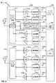
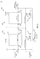
[0026]図2に、図1中のワイヤレスデバイス110の例示的な設計のブロック図を示す。この例示的な設計では、ワイヤレスデバイス110は、1次アンテナ210に結合されたトランシーバ220と、2次アンテナ212に結合されたトランシーバ222と、データプロセッサ/コントローラ280とを含む。トランシーバ220は、複数の周波数バンド、複数の無線技術、キャリアアグリゲーションなどをサポートするために、複数(K個)の受信機230pa〜230pkと複数(K個)の送信機250pa〜250pkとを含む。トランシーバ222は、複数の周波数バンド、複数の無線技術、キャリアアグリゲーション、受信ダイバーシティ、複数の送信アンテナから複数の受信アンテナへの多入力多出力(MIMO)送信などをサポートするために、複数(L個)の受信機230sa〜230slと複数(L個)の送信機250sa〜250slとを含む。
[0026] FIG. 2 shows a block diagram of an exemplary design of
[0027]図2に示されている例示的な設計では、各受信機230pa〜230pkおよび230sa〜230slは、それぞれ、LNA240pa〜240pkおよび240sa〜240slと、受信回路242pa〜242pkおよび242sa〜242slとを含む。データ受信では、1次アンテナ210は、基地局および/または他の送信機局から信号を受信し、受信RF信号を与え、その受信RF信号は、アンテナインターフェース回路224を介してルーティングされ、選択された受信機(たとえば、受信機230pk)に入力RF信号として提示される。同様にして、2次アンテナ212は、基地局および/または他の送信機局から信号を受信し、受信RF信号を与え、その受信RF信号は、アンテナインターフェース回路226を介してルーティングされ、選択された受信機に入力RF信号として提示される。
[0027] In the exemplary design shown in FIG. 2, each receiver 230pa-230pk and 230sa-230sl has LNA 240pa-240pk and 240sa-240sl and receive circuits 242pa-242pk and 242sa-242sl, respectively. Including. For data reception,
[0028]アンテナインターフェース回路224は、スイッチ、デュプレクサ、送信フィルタ、受信フィルタ、整合回路などを含み得る。以下の説明では、受信機230pkが選択された受信機であると仮定する。受信機230pk内で、LNA240pkが、入力RF信号を増幅し、出力RF信号を与える。
[0028] The
[0029]受信回路242pkは、出力RF信号をRFからベースバンドにダウンコンバートし、ダウンコンバートされた信号を増幅し、フィルタ処理し、データプロセッサ/コントローラ280にアナログ入力信号を与え得る。受信回路242pkは、ミキサ、フィルタ、増幅器、整合回路、発振器、局部発振器(LO)生成器、位相ロックループ(PLL:phase locked loop)などを含み得る。トランシーバ220、222中の各残りの受信機230pa、230sa、230slは、受信機230pkと同様の様式で動作し得る。
[0029] Receive circuit 242pk may downconvert the output RF signal from RF to baseband, amplify and filter the downconverted signal, and provide an analog input signal to data processor /
[0030]図2に示されている例示的な設計では、各送信機250pa〜250pkおよび250sa〜250slは、それぞれ、送信回路252pa〜252pkおよび252sa〜252slと、電力増幅器(PA)254pa〜254pkおよび254sa〜254slとを含む。データ送信では、データプロセッサ/コントローラ280は、送信されるべきデータを処理(たとえば、符号化および変調)し、選択された送信機にアナログ出力信号を与える。以下の説明では、送信機250paが選択された送信機であると仮定する。送信機250pa内で、送信回路252paは、アナログ出力信号を増幅し、フィルタ処理し、ベースバンドからRFにアップコンバートし、被変調RF信号を与える。送信回路252paは、増幅器、フィルタ、ミキサ、整合回路、発振器、LO生成器、PLLなどを含み得る。PA254paは、被変調RF信号を受信し、増幅し、送信RF信号を与える。送信RF信号は、アンテナインターフェース回路224中のカプラ296を通してルーティングされ、1次アンテナ210を介して送信される。トランシーバ220、222中の各残りの送信機250pk、250sa、25slは、送信機250paと同様の様式で動作し得る。
[0030] In the exemplary design shown in FIG. 2, each transmitter 250pa-250pk and 250sa-250s1, respectively, has a transmission circuit 252pa-252pk and 252sa-252sl and a power amplifier (PA) 254pa-254pk and 254sa to 254sl. For data transmission, the data processor /
[0031]図2は、受信機230pa〜230pkおよび230sa〜230slならびに送信機250pa〜250pkおよび250sa〜250slの例示的な設計を示している。受信機および送信機はまた、フィルタ、整合回路など、図2に示されていない他の回路を含み得る。トランシーバ220および222の全部または一部分が、1つまたは複数のアナログ集積回路(IC)、RF IC(RFIC)、混合信号ICなどの上に実装され得る。たとえば、LNA240pa〜240pkおよび240sa〜240slならびに受信回路242pa〜242pkおよび242sa〜242slは、RFICなどであり得る1つのモジュール上に実装され得る。トランシーバ220および222中の回路は他の様式でも実装され得る。
[0031] FIG. 2 shows an exemplary design of receivers 230pa-230pk and 230sa-230sl and transmitters 250pa-250pk and 250sa-250sl. The receiver and transmitter may also include other circuits not shown in FIG. 2, such as filters, matching circuits, and the like. All or a portion of
[0032]カプラ296は、電力増幅器254paから受信された信号の一部分を、フィードバック受信信号として、フィードバック受信経路を介してフィードバック受信回路298paに与える。フィードバック受信サーキュイティ298paは、RFフィルタ294を含む。RFフィルタ294は、抵抗容量性(RC)ノッチフィルタ292などの第2のフィルタと直列に結合された、楕円インダクティブキャパシタンス(LC)フィルタ290などの第1のフィルタを含む多段フィルタである。フィードバック受信サーキュイティ298paは、図5に関してさらに詳細に説明するものなど、楕円LCフィルタ290および/またはRCノッチフィルタ292がバイパスされることを可能にするバイパス回路(図示せず)をさらに含み得る。フィードバック受信サーキュイティ298paの出力(たとえば、RCノッチフィルタ292の出力)は、データプロセッサ/コントローラ280において制御回路284に与えられ得る。楕円LCフィルタ290は、比較的鋭いフィルタロールオフとともに(たとえば、送信機250paの)ビクティムバンドのキャリア周波数において比較的低いインバンドリップル(in-band ripple)またはインバンドドループ(in-band droop)を与えるように構成され得る。RCノッチフィルタ292は、アグレッサバンド(たとえば、送信機250saにおいて送信されたWLAN信号)のキャリア周波数を含む周波数ノッチ内の周波数成分を減衰させるように構成され得る。制御回路284は、RFフィルタ294から受信された信号の1つまたは複数の信号エネルギー測定を実行し、閉ループ電力制御動作の一部として送信機250paの送信電力を調整するように構成され得る。RFフィルタ294の例示的な実装形態が図4〜図6に関して説明され、RFフィルタ294の周波数応答の一例が図7に示されている。図7に関してさらに詳細に説明するように、RFフィルタ294は、ビクティムバンド周波数において比較的低い減衰(またはインバンド「ドループ」)を与え得、ビクティムバンド周波数の約3倍の周波数にあるアグレッサバンドの強い減衰を与え得る。その結果、−55dBmの3次相互変調ひずみが達成され得る。
[0032] Coupler 296 provides a portion of the signal received from power amplifier 254pa as a feedback received signal to feedback receiving circuit 298pa via a feedback receiving path. Feedback receiving circulatory 298 pa includes an
[0033]データプロセッサ/コントローラ280は、ワイヤレスデバイス110のための様々な機能を実行し得る。たとえば、データプロセッサ/コントローラ280は、受信機230pa〜230pkおよび230sa〜230slを介して受信されたデータと、送信機250pa〜250pkおよび250sa〜250slを介して送信されるべきデータとのための処理を実行し得る。データプロセッサ/コントローラ280は、トランシーバ220および222内の様々な回路の動作を制御し得る。メモリ282は、データプロセッサ/コントローラ280のプログラムコードおよびデータを記憶し得る。データプロセッサ/コントローラ280は、1つまたは複数の特定用途向け集積回路(ASIC)および/または他のIC上に実装され得る。制御サーキュイティ284はデータプロセッサ/コントローラ280内に含まれるものとして示されているが、他の実装形態では、制御サーキュイティ284は、データプロセッサ/コントローラ280の外部にあり得る。
[0033] The data processor /
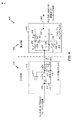
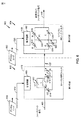
[0034]図3に、RFトランシーバ310とフロントエンドサブシステム350とを含むワイヤレス通信デバイス300の例示的な実施形態を示す。ワイヤレス通信デバイス300は、図1のワイヤレス通信デバイス110に対応し得る。フロントエンドサブシステム350は、送信周波数TX1において動作する第1の送信信号を、増幅し、フィルタ処理し、アンテナ355に制御可能に与える。さらに、RFトランシーバ310およびフロントエンドサブシステム350は、TX2の送信周波数において動作する第2の送信信号を、増幅し、フィルタ処理し、アンテナ365に制御可能に与える。
FIG. 3 illustrates an exemplary embodiment of a
[0035]フロントエンドサブシステム350は、RFトランシーバ310のデジタルアナログ変換器(DAC)342からアンテナ355に、TX1におけるアナログ信号を制御可能に結合する送信経路351を含む。送信経路351は、電力増幅器352と、パスバンドフィルタ354と、スイッチ356と、カプラ358との直列構成を含む。電力増幅器352は、DAC342から送信信号を受信し、接続341上の利得制御信号に従って送信信号の増幅されたバージョンをフォワーディングする。パスバンドフィルタ354は、TX1を下回る周波数およびTX1を上回る周波数において外来信号または雑音を減衰させる。増幅された送信信号のパスバンドフィルタ処理されたバージョンは、接続343上の制御信号に従って、スイッチ356によってカプラ358に選択的にフォワーディングされる。カプラ358は、アンテナ355などの第1のアンテナに結合されるように構成される。カプラ358は、増幅された送信信号のパスバンドフィルタ処理されたバージョンのエネルギーの大部分をアンテナ355に受け渡し、増幅された送信信号のパスバンドフィルタ処理されたバージョンの一部分は、接続359上でRFトランシーバ310のフィードバック経路314にフォワーディングされる。フィードバック経路314は、アナログデジタル変換器(ADC)346を含み、また、以下でさらに詳細に説明するように、第1のロケーション394において、第2のロケーション396において、または第3のロケーション398においてRFフィルタ294を含む。
[0035] The
[0036]同様に、送信経路361は、RFトランシーバ310のDAC344からアンテナ365に、TX2におけるアナログ信号を制御可能に結合する。送信経路361は、電力増幅器362と、パスバンドフィルタ364と、スイッチ366と、カプラ368との直列構成を含む。電力増幅器362は、DAC344から送信信号を受信し、接続345上の利得制御信号に従って送信信号の増幅されたバージョンをフォワーディングする。パスバンドフィルタ364は、TX2を下回る周波数およびTX2を上回る周波数において外来信号または雑音を減衰させる。増幅された送信信号のパスバンドフィルタ処理されたバージョンは、接続347上の制御信号に従って、スイッチ366によってカプラ368に選択的にフォワーディングされる。カプラ368は、アンテナ365などの第2のアンテナに結合されるように構成される。カプラ368は、信号エネルギーの大部分をアンテナ365に受け渡す。
[0036] Similarly, transmit
[0037]電力フィードバック信号を使用して(たとえば、TX1において)ローバンド送信信号を検出するために、比較的高い電力において(たとえば、TX2において)WLAN送信信号を同時に送信する間、RFフィルタ294は、フィードバック経路314中でWLANトランジット信号周波数をフィルタ処理するために使用され得る。図3の例示的な実施形態に示されているように、フィードバック経路314は、RFトランシーバ310における1つまたは複数の構成要素を含み得、またフロントエンドサブシステム350における1つまたは複数の構成要素を含み得る。したがって、RFフィルタ294は、フロントエンドサブシステム350中の第1のロケーション394において、RFトランシーバ310とフロントエンドサブシステム350との間のインターフェース303におけるまたはその近くの第2のロケーション396において、あるいはRFトランシーバ310中の第3のロケーション398において実装され得る。第3のロケーション398は、(RFフィルタ294がトランシーバチップ392上に位置する)オンチップ構成395に対応し得る。オンチップ構成395を使用してRFフィルタ294を実装することは、(たとえば、トランシーバチップ392の外部の)外部フィルタとしてRFフィルタ294を実装することと比較して、より低いコスト(たとえば、より低い部品表(BOM:bill of material))を生じ得る。フィードバック経路314に沿ったロケーションにかかわらず、RFフィルタ294は、第1の送信信号電力の一部分を受信し、変更されたフィードバック信号を生成するように構成され得る。変更されたフィードバック信号は、周波数の第1の範囲(TX1)にわたって比較的小さいインバンドドループ(たとえば、信号電力変化)を有し得、第2の送信周波数(TX2)において比較的大きい信号電力除去を有し得る。
[0037] While simultaneously transmitting the WLAN transmission signal at relatively high power (eg, at TX2) to detect the low-band transmission signal using the power feedback signal (eg, at TX1), the
[0038]接続341および接続345上の利得制御信号のうちの1つまたは複数は、ワイヤレス通信システム300から放射する送信信号電力をプログラム的に調整する、図2のデータプロセッサ/コントローラ280などのベースバンドプロセッサまたはコントローラから発生し得る。
[0038] One or more of the gain control signals on
[0039]接続343および接続347上のスイッチ制御信号のうちの1つまたは複数は、図2のデータプロセッサ/コントローラ280などのベースバンドプロセッサまたはコントローラから発生し得る。ベースバンドプロセッサまたはコントローラは、RFトランシーバ310およびフロントエンドサブシステム350の外側に位置し得る。接続343および接続347上のスイッチ制御信号は、第1および第2の送信信号がワイヤレス通信システム300からいつ放射するかのタイミングをプログラム的に調整するために、ベースバンドプロセッサまたはコントローラによって使用され得る。したがって、ベースバンドプロセッサまたはコントローラは、複数のワイヤレス通信プロトコルをサポートする適宜にタイミングをとられた送信信号の送信を協調させるために、1つまたは複数のアプリケーション、プログラム、構成要素、データベース、テーブル、またはモジュールに従って機能し得る。ベースバンドプロセッサまたはコントローラは、1つまたは複数の追加の内部または外部送信機(図示せず)からの干渉信号を回避するように(またはその影響を低減するように)プログラムされ得る。
[0039] One or more of the switch control signals on
[0040]例示的な実施形態では、ベースバンドプロセッサまたはコントローラは、電力推定を実行するためにフィードバック信号同相および直交位相成分を受信するように構成され得る。たとえば、受信フィードバック経路314は、図2の受信回路242に関して説明したように、1つまたは複数のミキサ、フィルタ、増幅器、整合回路、発振器、局部発振器(LO)生成器、および/または位相ロックループ(PLL)などの構成要素を含み得る。例示的な実施形態では、ベースバンドプロセッサまたはコントローラは、直流(DC)オフセットによる誤差を回避するために1つまたは複数の信号処理技法を利用するように構成され得る。例示的な実施形態では、ベースバンドプロセッサまたはコントローラは、RFトランシーバ310に送信信号と制御信号とを与え、RFトランシーバ310は、電力制御を実行するためにオンライン電力推定を行う。デジタルベースバンドモジュールは、フロントエンドサブシステム350によって送信信号に適用される利得を更新するために、推定された電力情報を使用し得る。
[0040] In an exemplary embodiment, the baseband processor or controller may be configured to receive feedback signal in-phase and quadrature components to perform power estimation. For example, the receive
[0041]図4は、多段RFフィルタ400の一実施形態(たとえば、図2および図3のRFフィルタ294の一実施形態)を示す例示的な図である。第1の段402は、カプラ(たとえば、図2のカプラ296または図3のカプラ358)に最も近く、ローパス楕円フィルタ410などの楕円LCフィルタを含む。ADC(たとえば、図3のADC346)に最も近い第2の段404は、RCノッチフィルタ430を含む。第1の段402の出力は、接続422を介して第2の段404の入力に結合される。
[0041] FIG. 4 is an exemplary diagram illustrating one embodiment of a multi-stage RF filter 400 (eg, one embodiment of
[0042]ローパス楕円フィルタ(LPEF:low-pass elliptical filter)410は、集積回路中の回路要素を使用して実装され得るRLC回路を含む。LPEF410は、第1のノード405(入力ノード)と第2のノード420(出力ノード)とに結合された第1のキャパシタ412を含む。インダクタ411は、第1のノード405と第2のノード420とに結合される。第2のキャパシタ414は、第1のノード405と第3のノード415とに結合される。第3のキャパシタ416は、第2のノード420と第3のノード415とに結合される。抵抗器413は、第2のノード420と第3のノード415とに結合される。
[0042] A low-pass elliptical filter (LPEF) 410 includes an RLC circuit that may be implemented using circuit elements in an integrated circuit. The
[0043]LPEF410は、接続422における出力信号によって特徴づけられる。出力信号は、周波数のパスバンド範囲中のリップル(「インバンドリップル」)および周波数のストップバンド範囲中のリップル、ならびにパスバンド周波数とストップバンド周波数との間の遷移(「フィルタロールオフ」)を含む。キャパシタンス値(第1のキャパシタ412のC1、第2のキャパシタ414のC2、および第3のキャパシタ416のC3)、抵抗器413の抵抗Rおよびインダクタ411のインダクタンスLのうちの1つまたは複数が、低いインバンドリップルと比較的鋭いフィルタロールオフとを引き起こすように選択され得る。少なくとも1つのそれぞれのキャパシタと並列な1つまたは複数の追加のインダクタは、パスバンドとストップバンドとの間の遷移のレートを変更するためにLPEF410に追加され得る。集積回路設計および製造の当業者は、多段フィルタ400の第1の段410から所望の特性を達成するために、回路要素を複製することと、抵抗値、インダクタンス値およびキャパシタンス値を選択することとが可能である。
[0043] The
[0044]図示された例示的な実施形態では、RCノッチフィルタ430はツイン「T」ノッチフィルタ(twin "T" notch filter)である。ツイン「T」ノッチフィルタ(TTNF)430は、集積回路中の回路要素を使用して実装され得るRC回路を含む。TTNF430は、第1のノード425(入力ノード)と第2のノード427とに結合された第1の抵抗器432を含む。第1のキャパシタ431は、第1のノード425と第3のノード429とに結合される。第2の抵抗器436は、第2のノード427と第4のノード437(出力ノード)とに結合される。第2のキャパシタ435は、第3のノード429と第4のノード437とに結合される。第3の抵抗器433および第3のキャパシタ434は、第2のノード427と第3のノード429との間に直列に結合される。第3の抵抗器433と、第1のキャパシタ431と、第2のキャパシタ435とは、第1の「T」を形成する。第3のキャパシタ434と、第1の抵抗器432と、第2の抵抗器436とは、第2の「T」を形成する。図示のように、第1のキャパシタ431および第2のキャパシタ435は、入力ノード425と出力ノード437との間の第1の抵抗器432および第2の抵抗器436と並列である。
[0044] In the illustrated exemplary embodiment,
[0045]TTNF430は、接続440上の出力信号によって特徴づけられ得る。出力信号は、ノッチ周波数において狭いストップバンドまたはノッチを含む。キャパシタンス値および抵抗値は、ノッチ周波数および/または1つまたは複数の他のフィルタ特性を設定するように選択され得る。一例として、抵抗器433は、抵抗器432の抵抗の1/2であり、抵抗器436の抵抗の1/2である抵抗を有し得る。さらに、キャパシタ434は、キャパシタ431のキャパシタンスの2倍であり、キャパシタ435のキャパシタンスの2倍であるキャパシタンスを有し得る。抵抗およびキャパシタンスが上記で与えられた比に正確に一致するほど、出力ノード440においてノッチは深くなる。集積回路設計および製造の当業者は、多段フィルタ400の第2の段430から所望の特性を達成するために、回路構成を複製することと、抵抗値およびキャパシタンス値を選択することとが可能である。
[0045]
[0046]図5は、多段RFフィルタ500の第1の段502および第2の段504の一方または両方がバイパスされることを可能にする回路要素および接続を示す図である。第1の段502は、図4の第1の段402に対応し得、第2の段504は図4の第2の段404に対応し得る。バイパス回路520は、フィードバック受信信号がRFフィルタ500の少なくとも一部分をバイパスすることを可能にするように構成される。バイパス回路520は、LPEF410に結合された(たとえば、LPEF410の入力501とLPEF410の出力503とに結合された)第1段バイパストランジスタ512を含む単段バイパス回路を含む。バイパス回路520は、RCノッチフィルタ430に結合された(たとえば、RCノッチフィルタ430の入力505とRCノッチフィルタ430の出力507とに結合された)第2段バイパストランジスタ514を含む。バイパス回路520は、LPEF410の入力501とRCノッチフィルタ430の出力507とに結合された多段バイパストランジスタ510を含む多段バイパス回路を含む。多段バイパストランジスタ510は、フィードバック受信信号が多段RFフィルタ500をバイパスする(すなわち、第1の段502の楕円LCフィルタ410をバイパスし、第2の段504のRCノッチフィルタ430をバイパスする)ことを可能にし得る。
[0046] FIG. 5 is a diagram illustrating circuit elements and connections that allow one or both of the
[0047]図5の回路図に示されているように、多段フィルタ500は、多段バイパストランジスタ510のゲートにおいて多段フィルタバイパスイネーブル信号509を受信したことに応答して、バイパスされ得る。多段バイパストランジスタ510が多段フィルタバイパスイネーブル信号509を受信するとき、多段バイパストランジスタ510は入力ノード405を出力ノード440に結合し、フィードバック信号(たとえば、図3のカプラ358からのTX電力フィードバック信号388)は多段フィルタ500をバイパスする。さらに示されているように、多段フィルタ500の第1の段502は、第1段バイパストランジスタ512のゲートにおいて第1段バイパスイネーブル信号511を受信したことに応答して、バイパスされ得る。第1段バイパストランジスタ512が第1段バイパスイネーブル信号511を受信するとき、入力ノード405は接続422に結合され、フィードバック信号はローパス楕円フィルタ410をバイパスし、第2の段504の入力にフォワーディングされる。このモードで動作しているとき、フィードバック信号は、ツイン「T」RCノッチフィルタ430によってフィルタ処理され、ローパス楕円フィルタ410によってフィルタ処理されない。逆に、第2の段504は、第2段バイパストランジスタ514のゲートにおいて第2段バイパスイネーブル信号513を受信したことに応答して、バイパスされ得る。第2段バイパストランジスタ514が第2段バイパスイネーブル信号513を受信するとき、接続422は出力ノード440に結合され、接続422上のローパスフィルタ処理されたフィードバック信号は、ツイン「T」RCノッチフィルタ430をバイパスする。このモードで動作しているとき、フィードバック信号は、LPEF410によってフィルタ処理され、ツイン「T」RCノッチフィルタ430によってフィルタ処理されない。各フィルタ段502、504がフィードバック受信経路上のフィードバック受信信号のエネルギーに影響を及ぼし得るので、フィルタ段502、504の一方または両方は、アグレッサバンド信号が送信されていない(または比較的低い送信電力を使用して送信されていない)とき、フィードバック受信信号を使用する閉ループ電力制御動作によってバイパスされ得る。
[0047] As shown in the circuit diagram of FIG. 5,
[0048]図6は、調整可能なフィルタ構成要素を有する多段フィルタ600の第1の段602および第2の段604を示す回路図である。多段フィルタ600は、例示的な、非限定的な例として、図2および図3のRFフィルタ294、図4のRFフィルタ400、または図5のRFフィルタ500に対応し得る。多段フィルタ600は、楕円LCフィルタ(たとえば、図4のLPEF410)が調整可能な構成要素を含む、第1の段602の実装形態を含む。たとえば、第1のキャパシタ612、第2のキャパシタ614、第3のキャパシタ616、および抵抗器613は、それぞれ、図4の第1のキャパシタ412、第2のキャパシタ414、第3のキャパシタ416、および抵抗器413の調整可能なバージョンに対応し得る。
[0048] FIG. 6 is a circuit diagram illustrating a
[0049]制御回路680は、楕円LCフィルタの少なくとも1つの構成要素の調整可能な値に対応するデジタルコード690を受信するように構成され得る。例示のために、制御ワードは、キャパシタ612、キャパシタ614、およびキャパシタ616のうちの1つまたは複数のキャパシタンスを変化させるために適用され得る様々な制御信号を与えるために、バス610上に与えられ得る。たとえば、キャパシタ612は、入力ノード405と接続422との間に並列に結合される複数の切替え容量性要素(switched capacitive element)を含み得る。制御回路680は、キャパシタ612のキャパシタンスを変更するために切替え容量性要素の各々に与えられるアクティブ化または非アクティブ化信号を生成するために、受信された制御ワード(または受信されたコードワードの一部分)を復号するように構成され得る。同様に、制御回路680は、キャパシタ614および/またはキャパシタ616の切替え可能容量性要素に対応するアクティブ化または非アクティブ化信号を生成するために、受信されたコードワード(または受信されたコードワードの部分)を復号するように構成され得る。バス610を介して通信された追加の制御信号が、同様に、抵抗器613の抵抗を変化させるためにLPEF410の制御入力に適用され得る。いくつかの実装形態では、第1のノード405と接続422とに結合されたインダクタ611は、インダクタ611のインダクタンスを変更するために制御回路680に応答し得る。したがって、様々な制御信号は、データまたは音声通信セッションに関与するときなど、通信デバイスが使用中である間、多段フィルタ600の第1の段602の1つまたは複数の特性を制御可能に調整するために使用され得る。
[0049] The
[0050]多段フィルタ600は、RCノッチフィルタ(たとえば、図4のツイン「T」RCノッチフィルタ430)が調整可能な構成要素を含む、第2の段604の実装形態をも含む。たとえば、第1の抵抗器632、第2の抵抗器636、第3の抵抗器633、第1のキャパシタ631、第2のキャパシタ635、および第3のキャパシタ634は、それぞれ、図4の第1の抵抗器432、第2の抵抗器436、第3の抵抗器433、第1のキャパシタ431、第2のキャパシタ435、および第3のキャパシタ434の調整可能なバージョンに対応し得る。
[0050] The
[0051]制御回路682は、RCノッチフィルタの少なくとも1つの受動構成要素の調整可能な値に対応するデジタルコード692を受信するように構成され得る。例示のために、第2の制御ワードは、多段フィルタ600の第2の段604におけるキャパシタンス値間の特定の関係を達成するために、キャパシタ634、キャパシタ631、およびキャパシタ635のうちの1つまたは複数のキャパシタンスを変化させるために適用される制御信号を導入するためにバス630上に与えられ得る。同様に、バス630を介して通信された1つまたは複数の追加の制御信号が、抵抗器633の抵抗または抵抗器632および抵抗器636のそれぞれの抵抗を変化させるために適用され得る。
[0051] The
[0052]したがって、多段フィルタ600の1つまたは複数の段の性能は、多段フィルタ600の1つまたは複数の構成要素の値を調整するために制御信号を使用して変更され得る。たとえば、図2の制御回路284は、それぞれ、バス610とバス630とを介して制御回路680、682において受信される1つまたは複数の制御ワードを生成し得る。例示のために、制御ワードは、アグレッサバンドのキャリア周波数に基づいておよび/またはビクティムバンドのキャリア周波数に基づいてなど、1つまたは複数のトランシーバの動作モードに基づいて、フィルタ性能を変更するために生成され得る。
[0052] Accordingly, the performance of one or more stages of
[0053]図6はフィルタ段602および604の特定の受動構成要素を調整可能であるものとして示しているが、他の実装形態では、より少数の構成要素が調整可能であり得るか、または追加の構成要素が調整可能であり得る。段602および604は調整可能な構成要素を含むものとして示されているが、他の実装形態では、段602または段604のうちの1つは調整可能な構成要素を含まないことがある。
[0053] Although FIG. 6 illustrates certain passive components of filter stages 602 and 604 as adjustable, in other implementations, fewer components may be adjustable or additional The components may be adjustable. Although
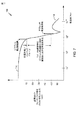
[0054]図7は、図4の多段フィルタ400の適用後の受信機フィードバック経路中の送信信号電力対送信信号周波数のプロット700である。送信信号周波数は水平軸に沿って示される。出力電力は、垂直軸上に信号強度(dB)によって示される。例示的な信号トレース710は、送信フィードバック経路中に挿入されるときの多段フィルタ400が、約775MHzから915MHzの間(ビクティムバンドの範囲)の所望の低いインバンドドループまたは変動と、約2.4GHzから2.48GHzの間の比較的近いWLAN周波数における極めて高い除去(信号損失)とを与えることを示す。ビクティムバンドにおける低いインバンドドループおよび鋭いロールオフは、図4、図5、または図6のLPEF410などの楕円LCフィルタによって引き起こされ得る。アグレッサバンドに近い大きな減衰は、図4、図5、または図6のツイン「T」RCノッチフィルタ430などのRFノッチフィルタの周波数ノッチに起因し得る。
[0054] FIG. 7 is a
[0055]例示的な実施形態では、図2および図3のRFフィルタ294、図4の多段フィルタ400、図5の多段フィルタ500、ならびに/または図6の多段フィルタ600は、当該の無線周波数信号の周波数に近い周波数を有する無線周波数信号を除去するために、任意の受信機に適用され得る。
[0055] In the exemplary embodiment,
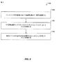
[0056]図8を参照すると、方法の例示的な実施形態が示されており、全体的に800と称される。方法800は、図1のワイヤレスデバイス110など、受信フィードバック経路中の多段フィルタをもつトランシーバを含むワイヤレスデバイスにおいて実行され得る。たとえば、方法800は、例示的な、非限定的な例として、図1または図2のワイヤレスデバイス110、図3の通信デバイス300、あるいは図4の多段フィルタ400、図5の多段フィルタ500、または図6の多段フィルタ600を含むデバイスによって実行され得る。
[0056] Referring to FIG. 8, an exemplary embodiment of the method is shown and generally designated 800. The
[0057]802において、フィードバック受信経路において無線周波数(RF)信号を受信する。たとえば、RF信号は、フィードバック受信信号(たとえば、フィードバック受信信号388)を含み得、図3のカプラ358を介してフィードバック経路314において受信され得る。RF信号は、図3の第1の送信経路351を介してアンテナ355に与えられた送信信号の少なくとも一部分に対応し得る。
[0057] At 802, a radio frequency (RF) signal is received in a feedback receive path. For example, the RF signal may include a feedback received signal (eg, feedback received signal 388) and may be received in
[0058]804において、RF信号を楕円インダクタンスキャパシタンス(LC)フィルタにおいてフィルタ処理する。楕円LCフィルタは、例示的な、非限定的な例として、図2および図3のRFフィルタ294、図4の多段フィルタ400、図5の多段フィルタ500、または図6の多段フィルタ600など、多段フィルタの第1の段であり得る。例示のために、RF信号は、例示的な、非限定的な例として、図2の楕円LCフィルタ290において、あるいは図4、図5、または図6のローパス楕円フィルタ310においてフィルタ処理され得る。
[0058] At 804, the RF signal is filtered in an elliptical inductance capacitance (LC) filter. The elliptical LC filter is a multistage filter, such as the
[0059]806において、楕円LCフィルタの出力を抵抗容量性(RC)ノッチフィルタを用いてフィルタ処理する。RCノッチフィルタは、例示的な、非限定的な例として、図2および図3のRFフィルタ294、図4の多段フィルタ400、図5の多段フィルタ500、または図6の多段フィルタ600など、多段フィルタの第2の段であり得る。例示のために、LCフィルタの出力は、例示的な、非限定的な例として、図2のRCノッチフィルタ292、あるいは図4、図5、または図6のRCノッチフィルタ430において受信され得る。
[0059] At 806, the output of the elliptical LC filter is filtered using a resistive capacitive (RC) notch filter. The RC notch filter is a multi-stage filter, such as the
[0060]楕円LCフィルタおよびRCノッチフィルタは、ワイヤレス通信デバイスのトランシーバチップ中のオンチップフィルタ中に含まれ得る。たとえば、楕円LCフィルタおよびRCノッチフィルタは、図3のトランシーバチップ392上のオンチップ構成395など、図3のRFトランシーバ310を含むトランシーバチップ中に含まれるオンチップフィルタであり得る。
[0060] An elliptical LC filter and an RC notch filter may be included in an on-chip filter in a transceiver chip of a wireless communication device. For example, the elliptical LC filter and the RC notch filter may be on-chip filters included in a transceiver chip that includes the
[0061]方法800はまた、楕円LCフィルタまたはRCノッチフィルタの少なくとも1つの構成要素の特性を調整することを含み得る。たとえば、1つまたは複数の受信された制御信号は、キャパシタ612、キャパシタ614、および/またはキャパシタ616のうちの1つまたは複数のキャパシタンスを変化させるために、抵抗器613の抵抗を変化させるために、あるいはそれらの任意の組合せのために適用され得る。代替的に、または追加として、1つまたは複数の受信された制御信号は、キャパシタ631、キャパシタ634、および/またはキャパシタ635のうちの1つまたは複数のキャパシタンスを変化させるために、抵抗器632、抵抗器633、および/または抵抗器636の抵抗を変化させるために、あるいはそれらの任意の組合せのために適用され得る。
[0061] The
[0062]方法800は、RF信号が楕円LCフィルタまたはRCノッチフィルタのうちの少なくとも1つをバイパスすることを可能にするように構成されたバイパス回路において、制御信号を受信することを含み得る。たとえば、制御信号は、図5の多段フィルタバイパスイネーブル信号509、第1段バイパスイネーブル信号511、または第2段バイパスイネーブル信号513のうちの1つまたは複数に対応し得る。
[0062]
[0063]図8は方法800の要素の特定の順序を示しているが、他の実施形態では、方法800の要素は別の順序で実行され得ることを理解されたい。さらに、方法800の要素のうちの2つまたはそれ以上(あるいはすべて)が、同時にまたは実質的に同時に実行され得る。たとえば、楕円LCフィルタとRCノッチフィルタとを含む多段フィルタは、時間変動受信フィードバック信号を連続的に受信し得、楕円LCフィルタおよびRCノッチフィルタは、直列に結合された構成において、受信された信号をフィルタ処理するように連続的に動作し得る。
[0063] Although FIG. 8 illustrates a particular order of the elements of
[0064]開示する実施形態とともに、楕円インダクタンスキャパシタンス(LC)フィルタ処理のための手段を含む装置について説明する。たとえば、楕円LCフィルタ処理のための手段は、図2の楕円LCフィルタ290、図4、図5、または図6のLPEF410、低いインバンドリップルと比較的鋭いフィルタロールオフとを導入する1つまたは複数の他のフィルタ回路、あるいはそれらの任意の組合せに対応し得る。
[0064] An apparatus including means for elliptical inductance capacitance (LC) filtering is described with the disclosed embodiments. For example, the means for elliptical LC filtering may be one of introducing
[0065]本装置は、楕円LCフィルタ処理のための手段に直列に結合された抵抗容量性(RC)ノッチフィルタ処理のための手段を含む。たとえば、RCノッチフィルタ処理のための手段は、図2のRCノッチフィルタ292、図4、図5、または図6のツイン「T」RCノッチフィルタ430、周波数ノッチ内の信号成分を減衰させる1つまたは複数の他のフィルタ回路、あるいはそれらの任意の組合せに対応し得る。
[0065] The apparatus includes means for resistive capacitive (RC) notch filtering coupled in series to means for elliptical LC filtering. For example, means for RC notch filter processing include
[0066]楕円LCフィルタ処理のための手段およびRCノッチフィルタ処理のための手段は、フィードバック受信経路によって受信された無線周波数(RF)信号をフィルタ処理するように構成され得る。たとえば、楕円LCフィルタ処理のための手段およびRCノッチフィルタ処理のための手段は、図2および図3のRFフィルタ294の段、図4の多段フィルタ400の段、図5の多段フィルタ500の段、図6の多段フィルタ600の段、フィルタ回路のうちの1つまたは複数の段、またはそれらの任意の組合せに対応し得る。
[0066] The means for elliptical LC filtering and the means for RC notch filtering may be configured to filter a radio frequency (RF) signal received by the feedback receive path. For example, the means for elliptical LC filter processing and the means for RC notch filter processing include the stages of the
[0067]例示的な実施形態では、楕円LCフィルタ処理のための手段およびRCノッチフィルタ処理のための手段は、トランシーバチップ中に含まれる。たとえば、楕円LCフィルタ処理のための手段およびRCノッチフィルタ処理のための手段は、図3のオンチップ構成395を有するRFフィルタ294などのRFフィルタに対応し得る。楕円LCフィルタ処理のための手段およびRCノッチフィルタ処理のための手段は、ビクティムバンドとアグレッサバンドとに関して説明するものなど、RF信号のキャリア周波数の第3高調波に対応するRF信号の成分を減衰させるように構成されるフィルタ処理のための手段に含まれ得る。
[0067] In an exemplary embodiment, means for elliptical LC filtering and means for RC notch filtering are included in the transceiver chip. For example, the means for elliptical LC filtering and the means for RC notch filtering may correspond to an RF filter such as
[0068]本装置は、楕円LCフィルタ処理のための手段またはRCノッチフィルタ処理のための手段のうちの少なくとも1つをバイパスするための手段をも含み得る。たとえば、バイパスするための手段は、フィードバック受信機信号が楕円LCフィルタ処理のための手段をバイパスし、RCノッチフィルタ処理のための手段をバイパスすることを可能にする多段バイパス回路を含み得る。例示のために、バイパスするための手段は、図5のバイパス回路520、図5の多段バイパストランジスタ510、図5の第1段バイパストランジスタ512、図5の第2段バイパストランジスタ514、フィルタ処理のための手段の少なくとも一部分をバイパスするように構成された1つまたは複数の他の回路、またはそれらの任意の組合せを含み得る。
[0068] The apparatus may also include means for bypassing at least one of means for elliptical LC filtering or means for RC notch filtering. For example, the means for bypassing may include a multi-stage bypass circuit that allows the feedback receiver signal to bypass the means for elliptical LC filtering and bypass the means for RC notch filtering. For purposes of illustration, the means for bypassing are:
[0069]多段フィルタをもつフィードバック受信経路は、1つまたは複数のIC、アナログIC、RFIC、混合信号IC、ASIC、プリント回路板(PCB)、電子デバイスなどの上に実装され得る。また、多段フィルタは、相補型金属酸化物半導体(CMOS)、NチャネルMOS(NMOS)、PチャネルMOS(PMOS)、バイポーラ接合トランジスタ(BJT)、バイポーラCMOS(BiCMOS)、シリコンゲルマニウム(SiGe)、ガリウムヒ素(GaAs)、ヘテロ接合バイポーラトランジスタ(HBT)、高電子移動度トランジスタ(HEMT)、シリコンオンインシュレータ(SOI)など、様々なICプロセス技術を使用して作製され得る。 [0069] A feedback receive path with a multi-stage filter may be implemented on one or more ICs, analog ICs, RFICs, mixed signal ICs, ASICs, printed circuit boards (PCBs), electronic devices, and the like. The multi-stage filter includes complementary metal oxide semiconductor (CMOS), N channel MOS (NMOS), P channel MOS (PMOS), bipolar junction transistor (BJT), bipolar CMOS (BiCMOS), silicon germanium (SiGe), gallium. It can be fabricated using various IC process technologies such as arsenic (GaAs), heterojunction bipolar transistor (HBT), high electron mobility transistor (HEMT), silicon on insulator (SOI).
[0070]本明細書で説明するように受信フィードバック経路の上に多段フィルタを実装する装置は、スタンドアロンデバイスであり得るか、またはより大きいデバイスの一部であり得る。デバイスは、(i)スタンドアロンIC、(ii)データおよび/または命令を記憶するためのメモリICを含み得る1つまたは複数のICのセット、(iii)RF受信機(RFR)またはRF送信機/受信機(RTR)などのRFIC、(iv)移動局モデム(MSM)などのASIC、(v)他のデバイス内に埋め込まれ得るモジュール、(vi)受信機、セルラーフォン、ワイヤレスデバイス、ハンドセット、またはモバイルユニット、(vii)その他であり得る。 [0070] An apparatus that implements a multi-stage filter on the receive feedback path as described herein may be a stand-alone device or may be part of a larger device. The device may comprise (i) a stand-alone IC, (ii) a set of one or more ICs that may include a memory IC for storing data and / or instructions, (iii) an RF receiver (RFR) or an RF transmitter / An RFIC such as a receiver (RTR), (iv) an ASIC such as a mobile station modem (MSM), (v) a module that can be embedded in another device, (vi) a receiver, cellular phone, wireless device, handset, or It can be a mobile unit, (vii) others.
[0071]1つまたは複数の例示的な設計では、説明した機能は、ハードウェア、ソフトウェア、ファームウェア、またはそれらの任意の組合せで実装され得る。ソフトウェアで実装される場合、機能は、1つまたは複数の命令またはコードとしてコンピュータ可読媒体上に記憶され得る。コンピュータ可読媒体は、ある場所から別の場所へのコンピュータプログラムの転送を可能にする任意の媒体を含む、コンピュータ記憶媒体とコンピュータ通信媒体の両方を含む。記憶媒体は、コンピュータによってアクセスされ得る任意の利用可能な媒体であり得る。例示的な実施形態では、記憶媒体は、データを記憶するストレージデバイスである。ストレージデバイスは信号ではない。ストレージデバイスは、物理ストレージ材料の光反射率または磁気配向、トランジスタのフローティングゲートにまたはキャパシタのプレートに記憶された電荷量などに基づいてデータを記憶し得る。限定ではなく例として、コンピュータ可読媒体は、RAM、ROM、EEPROM(登録商標)、CD−ROMまたは他の光ディスクストレージ、磁気ディスクストレージまたは他の磁気ストレージデバイス、あるいは命令またはデータ構造の形態のプログラムコードを搬送または記憶するために使用され得、コンピュータによってアクセスされ得る、任意の他の媒体を備えることができる。また、いかなる接続もコンピュータ可読媒体と適切に呼ばれる。たとえば、ソフトウェアが、同軸ケーブル、光ファイバーケーブル、ツイストペア、デジタル加入者回線(DSL)、または赤外線、無線、およびマイクロ波などのワイヤレス技術を使用して、ウェブサイト、サーバ、または他のリモートソースから送信される場合、同軸ケーブル、光ファイバーケーブル、ツイストペア、DSL、または赤外線、無線、およびマイクロ波などのワイヤレス技術は、媒体の定義に含まれる。本明細書で使用するディスク(disk)およびディスク(disc)は、コンパクトディスク(disc)(CD)、レーザーディスク(登録商標)(disc)、光ディスク(disc)、デジタル多用途ディスク(disc)(DVD)、フロッピー(登録商標)ディスク(disk)およびblu−ray(登録商標)ディスク(disc)を含み、ここで、ディスク(disk)は、通常、データを磁気的に再生し、ディスク(disc)は、データをレーザーで光学的に再生する。上記の組合せもコンピュータ可読媒体の範囲内に含まれるべきである。 [0071] In one or more exemplary designs, the functions described may be implemented in hardware, software, firmware, or any combination thereof. If implemented in software, the functions may be stored on a computer-readable medium as one or more instructions or code. Computer-readable media includes both computer storage media and computer communication media including any medium that facilitates transfer of a computer program from one place to another. A storage media may be any available media that can be accessed by a computer. In the exemplary embodiment, the storage medium is a storage device that stores data. The storage device is not a signal. The storage device may store data based on the light reflectivity or magnetic orientation of the physical storage material, the amount of charge stored on the floating gate of the transistor or on the plate of the capacitor, and the like. By way of example, and not limitation, computer-readable media includes RAM, ROM, EEPROM®, CD-ROM or other optical disk storage, magnetic disk storage or other magnetic storage device, or program code in the form of instructions or data structures. Any other medium that can be used to transport or store and that can be accessed by a computer can be provided. Any connection is also properly termed a computer-readable medium. For example, software sends from a website, server, or other remote source using coaxial cable, fiber optic cable, twisted pair, digital subscriber line (DSL), or wireless technologies such as infrared, wireless, and microwave Where included, coaxial technology, fiber optic cable, twisted pair, DSL, or wireless technologies such as infrared, radio, and microwave are included in the definition of media. As used herein, a disk and a disc are a compact disc (CD), a laser disc (registered trademark) (disc), an optical disc (disc), a digital versatile disc (DVD). ), Floppy disk, and blu-ray disk, where the disk normally reproduces data magnetically, and the disk is The data is optically reproduced with a laser. Combinations of the above should also be included within the scope of computer-readable media.
[0072]本明細書で使用する「構成要素」、「データベース」、「モジュール」、「システム」などの用語は、ハードウェア、ファームウェア、ハードウェアとソフトウェアの組合せ、ソフトウェア、または実行中のソフトウェアなど、コンピュータ関連のエンティティを指すものとする。例示のために、図2のデータプロセッサ280は、本明細書で説明したように、フィードバック受信信号の多段フィルタ処理に基づいて、閉ループ電力制御動作中に1つまたは複数の利得制御信号の値を選択するためのプログラム命令、図5に関して説明したように、1つまたは複数のバイパスイネーブル信号の値を選択するためのプログラム命令、図6に関して説明したように、調整可能な受動構成要素の1つまたは複数の値を選択するためのプログラム命令、あるいはそれらの任意の組合せを実行し得る。例示的な、非限定的な例として、構成要素は、プロセッサ上で実行しているプロセス、プロセッサ、オブジェクト、実行ファイル、実行スレッド、プログラム、および/またはコンピュータであり得る。例として、コンピューティングデバイス上で実行しているアプリケーションと、そのコンピューティングデバイスの両方が構成要素であり得る。1つまたは複数の構成要素がプロセスおよび/または実行スレッド内に常駐し得、1つの構成要素が1つのコンピュータ上に配置され得、および/または2つまたはそれ以上のコンピュータ間に分散され得る。さらに、構成要素は、データ構造を記憶している様々なコンピュータ可読媒体から実行し得る。
[0072] As used herein, the terms "component", "database", "module", "system", etc. refer to hardware, firmware, a combination of hardware and software, software, or running software, etc. , And refers to a computer-related entity. For purposes of illustration, the
[0073]選択された態様について詳細に図示および説明したが、以下の特許請求の範囲によって定義されるように、本発明の範囲から逸脱することなく、様々な置換および改変を本明細書で行い得ることを理解されよう。 [0073] Although selected embodiments have been shown and described in detail, various substitutions and modifications may be made herein without departing from the scope of the invention as defined by the following claims. You will understand that you get.
[0073]選択された態様について詳細に図示および説明したが、以下の特許請求の範囲によって定義されるように、本発明の範囲から逸脱することなく、様々な置換および改変を本明細書で行い得ることを理解されよう。
以下に、本願出願の当初の特許請求の範囲に記載された発明を付記する。
[C1]
楕円インダクタンスキャパシタンス(LC)フィルタと、
前記楕円LCフィルタに直列に結合された抵抗容量性(RC)ノッチフィルタと、を備え、
前記楕円LCフィルタおよび前記RCノッチフィルタが、フィードバック受信経路によって受信された無線周波数(RF)信号をフィルタ処理するように構成された、装置。
[C2]
前記楕円LCフィルタおよび前記RCノッチフィルタが、トランシーバチップ中に含まれるオンチップフィルタを備える、C1に記載の装置。
[C3]
前記RF信号が前記楕円LCフィルタまたは前記RCノッチフィルタのうちの少なくとも1つをバイパスすることを可能にするように構成されたバイパス回路をさらに備える、C1に記載の装置。
[C4]
前記バイパス回路が、
前記楕円LCフィルタに結合された第1段バイパストランジスタと、
前記RCノッチフィルタに結合された第2段バイパストランジスタと
を備える、C3に記載の装置。
[C5]
前記バイパス回路が、前記楕円LCフィルタの入力と前記RCノッチフィルタの出力とに結合された多段バイパストランジスタを備える、C3に記載の装置。
[C6]
前記楕円LCフィルタが調整可能な構成要素を含む、C1に記載の装置。
[C7]
前記RCノッチフィルタが調整可能な構成要素を含む、C1に記載の装置。
[C8]
前記楕円LCフィルタが、
第1のノードと第2のノードとに結合された第1のキャパシタと、
前記第1のノードと前記第2のノードとに結合されたインダクタとを備える、C1に記載の装置。
[C9]
前記楕円LCフィルタが、
前記第1のノードと第3のノードとに結合された第2のキャパシタと、
前記第2のノードと前記第3のノードとに結合された第3のキャパシタと、
前記第2のノードと前記第3のノードとに結合された抵抗器とをさらに備える、C8に記載の装置。
[C10]
前記RCノッチフィルタが、
第1のノードと第2のノードとに結合された第1の抵抗器と、
前記第1のノードと第3のノードとに結合された第1のキャパシタと、
前記第2のノードと第4のノードとに結合された第2の抵抗器と、
前記第3のノードと前記第4のノードとに結合された第2のキャパシタとを備える、C1に記載の装置。
[C11]
前記RCノッチフィルタが、前記第2のノードと前記第3のノードとの間で直列に結合された第3の抵抗器と第3のキャパシタとをさらに備える、C10に記載の装置。
[C12]
前記フィードバック受信経路がRF送信経路のカプラに結合される、C1に記載の装置。
[C13]
前記楕円LCフィルタおよび前記RCノッチフィルタが、前記RF信号のキャリア周波数の第3高調波に対応する前記RF信号の成分を減衰させるように構成されたRFフィルタ中に含まれる、C1に記載の装置。
[C14]
楕円インダクタンスキャパシタンス(LC)フィルタ処理のための手段と、
楕円LCフィルタ処理のための前記手段に直列に結合された抵抗容量性(RC)ノッチフィルタ処理のための手段と、を備え、
楕円LCフィルタ処理のための前記手段およびRCノッチフィルタ処理のための前記手段が、フィードバック受信経路によって受信された無線周波数(RF)信号をフィルタ処理するように構成された、装置。
[C15]
楕円LCフィルタ処理のための前記手段およびRFノッチフィルタ処理のための前記手段が、トランシーバチップ中に含まれる、C14に記載の装置。
[C16]
楕円LCフィルタ処理のための前記手段またはRCノッチフィルタ処理のための前記手段のうちの少なくとも1つをバイパスするための手段をさらに備える、C14に記載の装置。
[C17]
楕円LCフィルタ処理のための前記手段またはRCノッチフィルタ処理のための前記手段が、調整可能な構成要素を含む、C14に記載の装置。
[C18]
フィードバック受信経路において無線周波数(RF)信号を受信することと、
楕円インダクタンスキャパシタンス(LC)フィルタにおいて前記RF信号をフィルタ処理することと、
抵抗容量性(RC)ノッチフィルタを用いて前記楕円LCフィルタの出力をフィルタ処理することと
を備える方法。
[C19]
前記楕円LCフィルタまたは前記RCノッチフィルタの少なくとも1つの構成要素の特性を調整することをさらに備える、C18に記載の方法。
[C20]
前記RF信号が前記楕円LCフィルタまたは前記RCノッチフィルタのうちの少なくとも1つをバイパスすることを可能にするように構成されたバイパス回路において、制御信号を受信することをさらに備える、C18に記載の方法。
[0073] Although selected embodiments have been shown and described in detail, various substitutions and modifications may be made herein without departing from the scope of the invention as defined by the following claims. You will understand that you get.
Hereinafter, the invention described in the scope of claims of the present application will be appended.
[C1]
An elliptical inductance capacitance (LC) filter;
A resistive capacitive (RC) notch filter coupled in series with the elliptical LC filter;
The apparatus, wherein the elliptical LC filter and the RC notch filter are configured to filter radio frequency (RF) signals received by a feedback receive path.
[C2]
The apparatus of C1, wherein the elliptical LC filter and the RC notch filter comprise on-chip filters included in a transceiver chip.
[C3]
The apparatus of C1, further comprising a bypass circuit configured to allow the RF signal to bypass at least one of the elliptical LC filter or the RC notch filter.
[C4]
The bypass circuit is
A first stage bypass transistor coupled to the elliptical LC filter;
A second stage bypass transistor coupled to the RC notch filter;
The apparatus according to C3, comprising:
[C5]
The apparatus of C3, wherein the bypass circuit comprises a multi-stage bypass transistor coupled to an input of the elliptical LC filter and an output of the RC notch filter.
[C6]
The apparatus of C1, wherein the elliptical LC filter includes adjustable components.
[C7]
The apparatus of C1, wherein the RC notch filter includes adjustable components.
[C8]
The elliptical LC filter is
A first capacitor coupled to the first node and the second node;
The apparatus of C1, comprising an inductor coupled to the first node and the second node.
[C9]
The elliptical LC filter is
A second capacitor coupled to the first node and a third node;
A third capacitor coupled to the second node and the third node;
The apparatus of C8, further comprising a resistor coupled to the second node and the third node.
[C10]
The RC notch filter is
A first resistor coupled to the first node and the second node;
A first capacitor coupled to the first node and a third node;
A second resistor coupled to the second node and a fourth node;
The apparatus of C1, comprising a second capacitor coupled to the third node and the fourth node.
[C11]
The apparatus of C10, wherein the RC notch filter further comprises a third resistor and a third capacitor coupled in series between the second node and the third node.
[C12]
The apparatus of C1, wherein the feedback receive path is coupled to a coupler of an RF transmit path.
[C13]
The apparatus of C1, wherein the elliptical LC filter and the RC notch filter are included in an RF filter configured to attenuate a component of the RF signal corresponding to a third harmonic of a carrier frequency of the RF signal .
[C14]
Means for elliptical inductance capacitance (LC) filtering;
Means for resistive capacitive (RC) notch filtering coupled in series with said means for elliptical LC filtering;
The apparatus, wherein the means for elliptical LC filtering and the means for RC notch filtering are configured to filter radio frequency (RF) signals received by a feedback receive path.
[C15]
The apparatus of C14, wherein the means for elliptical LC filtering and the means for RF notch filtering are included in a transceiver chip.
[C16]
The apparatus of C14, further comprising means for bypassing at least one of the means for elliptical LC filtering or the means for RC notch filtering.
[C17]
The apparatus of C14, wherein the means for elliptical LC filtering or the means for RC notch filtering includes adjustable components.
[C18]
Receiving a radio frequency (RF) signal in a feedback receive path;
Filtering the RF signal in an elliptical inductance capacitance (LC) filter;
Filtering the output of the elliptical LC filter using a resistive capacitive (RC) notch filter;
A method comprising:
[C19]
The method of C18, further comprising adjusting a characteristic of at least one component of the elliptical LC filter or the RC notch filter.
[C20]
The method of C18, further comprising receiving a control signal in a bypass circuit configured to allow the RF signal to bypass at least one of the elliptical LC filter or the RC notch filter. Method.
Claims (20)
前記楕円LCフィルタに直列に結合された抵抗容量性(RC)ノッチフィルタと、
を備え、
前記楕円LCフィルタおよび前記RCノッチフィルタが、フィードバック受信経路によって受信された無線周波数(RF)信号をフィルタ処理するように構成された、装置。 An elliptical inductance capacitance (LC) filter;
A resistive capacitive (RC) notch filter coupled in series to the elliptical LC filter;
With
The apparatus, wherein the elliptical LC filter and the RC notch filter are configured to filter radio frequency (RF) signals received by a feedback receive path.
前記楕円LCフィルタに結合された第1段バイパストランジスタと、
前記RCノッチフィルタに結合された第2段バイパストランジスタと
を備える、請求項3に記載の装置。 The bypass circuit is
A first stage bypass transistor coupled to the elliptical LC filter;
4. The apparatus of claim 3, comprising a second stage bypass transistor coupled to the RC notch filter.
第1のノードと第2のノードとに結合された第1のキャパシタと、
前記第1のノードと前記第2のノードとに結合されたインダクタと
を備える、請求項1に記載の装置。 The elliptical LC filter is
A first capacitor coupled to the first node and the second node;
The apparatus of claim 1, comprising an inductor coupled to the first node and the second node.
前記第1のノードと第3のノードとに結合された第2のキャパシタと、
前記第2のノードと前記第3のノードとに結合された第3のキャパシタと、
前記第2のノードと前記第3のノードとに結合された抵抗器と
をさらに備える、請求項8に記載の装置。 The elliptical LC filter is
A second capacitor coupled to the first node and a third node;
A third capacitor coupled to the second node and the third node;
The apparatus of claim 8, further comprising a resistor coupled to the second node and the third node.
第1のノードと第2のノードとに結合された第1の抵抗器と、
前記第1のノードと第3のノードとに結合された第1のキャパシタと、
前記第2のノードと第4のノードとに結合された第2の抵抗器と、
前記第3のノードと前記第4のノードとに結合された第2のキャパシタと
を備える、請求項1に記載の装置。 The RC notch filter is
A first resistor coupled to the first node and the second node;
A first capacitor coupled to the first node and a third node;
A second resistor coupled to the second node and a fourth node;
The apparatus of claim 1, comprising a second capacitor coupled to the third node and the fourth node.
楕円LCフィルタ処理のための前記手段に直列に結合された抵抗容量性(RC)ノッチフィルタ処理のための手段と、
を備え、
楕円LCフィルタ処理のための前記手段およびRCノッチフィルタ処理のための前記手段が、フィードバック受信経路によって受信された無線周波数(RF)信号をフィルタ処理するように構成された、装置。 Means for elliptical inductance capacitance (LC) filtering;
Means for resistive capacitive (RC) notch filtering coupled in series with said means for elliptical LC filtering;
With
The apparatus, wherein the means for elliptical LC filtering and the means for RC notch filtering are configured to filter radio frequency (RF) signals received by a feedback receive path.
楕円インダクタンスキャパシタンス(LC)フィルタにおいて前記RF信号をフィルタ処理することと、
抵抗容量性(RC)ノッチフィルタを用いて前記楕円LCフィルタの出力をフィルタ処理することと
を備える方法。 Receiving a radio frequency (RF) signal in a feedback receive path;
Filtering the RF signal in an elliptical inductance capacitance (LC) filter;
Filtering the output of the elliptical LC filter using a resistive capacitive (RC) notch filter.
Applications Claiming Priority (5)
| Application Number | Priority Date | Filing Date | Title |
|---|---|---|---|
| US201462004758P | 2014-05-29 | 2014-05-29 | |
| US62/004,758 | 2014-05-29 | ||
| US14/664,622 US9762274B2 (en) | 2014-05-29 | 2015-03-20 | Feedback receive path with RF filter |
| US14/664,622 | 2015-03-20 | ||
| PCT/US2015/030403 WO2015183548A1 (en) | 2014-05-29 | 2015-05-12 | Feedback receive path with rf filter |
Publications (2)
| Publication Number | Publication Date |
|---|---|
| JP2017520168A true JP2017520168A (en) | 2017-07-20 |
| JP2017520168A5 JP2017520168A5 (en) | 2018-06-07 |
Family
ID=54699540
Family Applications (1)
| Application Number | Title | Priority Date | Filing Date |
|---|---|---|---|
| JP2016569647A Ceased JP2017520168A (en) | 2014-05-29 | 2015-05-12 | Feedback reception path using RF filter |
Country Status (6)
| Country | Link |
|---|---|
| US (1) | US9762274B2 (en) |
| EP (1) | EP3149861B1 (en) |
| JP (1) | JP2017520168A (en) |
| KR (1) | KR20170012256A (en) |
| CN (1) | CN106416087B (en) |
| WO (1) | WO2015183548A1 (en) |
Families Citing this family (16)
| Publication number | Priority date | Publication date | Assignee | Title |
|---|---|---|---|---|
| JP6500913B2 (en) * | 2015-01-21 | 2019-04-17 | 株式会社村田製作所 | High frequency circuit component and communication device |
| US9549406B1 (en) * | 2015-09-14 | 2017-01-17 | Elwha Llc | Automatically adjustable radiofrequency link |
| DE102016114663A1 (en) | 2016-08-08 | 2018-02-08 | Snaptrack, Inc. | multiplexer |
| US10348528B2 (en) | 2016-11-11 | 2019-07-09 | Qualcomm Incorporation | Systems and methods to provide upconverting with notch filtering |
| KR20190024068A (en) | 2017-08-31 | 2019-03-08 | (주)에스알테크날러지 | A method of manufacturing an RF filter using of laser trench |
| KR20190024067A (en) | 2017-08-31 | 2019-03-08 | (주)에스알테크날러지 | A method of manufacturing an RF filter using of laser etching |
| CN110022160B (en) | 2017-12-07 | 2022-07-05 | 英飞凌科技股份有限公司 | System and method for radio frequency filter |
| US10547289B2 (en) * | 2018-04-25 | 2020-01-28 | Qualcomm Incorporated | High order miller N-path filter |
| WO2019235181A1 (en) * | 2018-06-04 | 2019-12-12 | 株式会社村田製作所 | Radio frequency front-end module and communication device |
| US10951202B2 (en) | 2018-07-20 | 2021-03-16 | Futurewei Technologies, Inc. | Method and apparatus for RC/CR phase error calibration of measurement receiver |
| CN110444893B (en) * | 2019-08-16 | 2020-05-26 | 歌尔科技有限公司 | Monopole antenna bandwidth adjusting method and system |
| CN111600625A (en) * | 2020-05-14 | 2020-08-28 | 锐石创芯(深圳)科技有限公司 | Radio frequency front-end circuit and radio frequency front-end device |
| KR102656705B1 (en) * | 2020-05-25 | 2024-04-11 | 삼성전자주식회사 | A radio frequency transmitter configured to select output power control range and an wireless communication device including the same |
| US11736091B2 (en) | 2021-12-20 | 2023-08-22 | International Business Machines Corporation | Baseband filter for current-mode signal path |
| US20230253990A1 (en) * | 2022-02-10 | 2023-08-10 | Qualcomm Incorporated | Multi-band input stage of receiver with selectable third harmonic filter |
| WO2024019493A1 (en) * | 2022-07-20 | 2024-01-25 | 삼성전자 주식회사 | Electronic device and method for controlling communication by electronic device |
Citations (6)
| Publication number | Priority date | Publication date | Assignee | Title |
|---|---|---|---|---|
| US5694082A (en) * | 1995-02-22 | 1997-12-02 | Mikom Gmbh | Circuit arrangement for determining intermodulation products |
| WO2006090436A1 (en) * | 2005-02-23 | 2006-08-31 | Renesas Technology Corp. | Receiving circuit |
| JP2006295522A (en) * | 2005-04-11 | 2006-10-26 | Sony Ericsson Mobilecommunications Japan Inc | Portable telephone terminal |
| US20090280766A1 (en) * | 2008-05-07 | 2009-11-12 | Ahmadreza Rofougaran | Method And System For On-Demand Signal Notching In A Receiver |
| WO2013156189A1 (en) * | 2012-04-16 | 2013-10-24 | Alcatel Lucent | Cross-talk cancellation in a multiband transceiver |
| US20140029683A1 (en) * | 2012-07-26 | 2014-01-30 | Telefonaktiebolaget L M Ericsson (Publ) | Multi-Band Observation Receiver |
Family Cites Families (29)
| Publication number | Priority date | Publication date | Assignee | Title |
|---|---|---|---|---|
| US3643173A (en) * | 1970-05-18 | 1972-02-15 | Gen Electric | Tuneable microelectronic active band-pass filter |
| US4099125A (en) * | 1976-06-23 | 1978-07-04 | Motorola, Inc. | Frequency error correction circuit |
| GB2168864A (en) * | 1984-12-19 | 1986-06-25 | Philips Electronic Associated | Radio receiver/transmitter filters |
| US5345375A (en) * | 1991-12-16 | 1994-09-06 | Regents Of The University Of Minnesota | System and method for reducing harmonic currents by current injection |
| US5745523A (en) | 1992-10-27 | 1998-04-28 | Ericsson Inc. | Multi-mode signal processing |
| US5663675A (en) | 1995-06-07 | 1997-09-02 | American Microsystems, Inc. | Multiple stage tracking filter using a self-calibrating RC oscillator circuit |
| GB9601488D0 (en) * | 1996-01-25 | 1996-03-27 | Rca Thomson Licensing Corp | Time reversal filter |
| US20020085724A1 (en) * | 1997-02-06 | 2002-07-04 | James A. Grasfield | Stethoscope communication and remote diagnosis system |
| US6975843B2 (en) * | 2000-12-21 | 2005-12-13 | Telefonaktiebolaget L M Ericsson (Publ) | Method and an arrangement relating to telecommunications systems |
| JP3805221B2 (en) | 2001-09-18 | 2006-08-02 | 株式会社日立国際電気 | Distortion compensation device |
| US7761067B1 (en) * | 2003-05-15 | 2010-07-20 | Marvell International Ltd. | Iterative filter circuit calibration |
| US20070140391A1 (en) | 2005-12-20 | 2007-06-21 | Jianping Pan | Rf complex bandpass-notch filter for rf receiver and tv tuner |
| US7368999B2 (en) * | 2006-07-10 | 2008-05-06 | Jds Uniphase Corporation | DC offset cancellation for a trans-impedance amplifier |
| JP4903217B2 (en) | 2006-10-25 | 2012-03-28 | パナソニック株式会社 | Transmission method and transmission apparatus |
| US8237509B2 (en) | 2007-02-23 | 2012-08-07 | Qualcomm, Incorporated | Amplifier with integrated filter |
| US8295396B2 (en) * | 2007-08-22 | 2012-10-23 | Texas Instruments Incorporated | System and method for power control in a wireless transmitter |
| US8014373B2 (en) | 2007-09-19 | 2011-09-06 | John Mezzalingua Associates, Inc. | Filtered antenna assembly |
| US8090332B2 (en) * | 2007-12-12 | 2012-01-03 | Qualcomm, Incorporated | Tracking filter for a receiver |
| EP2249482A1 (en) | 2008-04-17 | 2010-11-10 | Panasonic Corporation | Receiver and electronic device using the same |
| US8688045B2 (en) | 2008-11-19 | 2014-04-01 | Qualcomm Incorporated | FM transmitter and non-FM receiver integrated on single chip |
| US8058949B2 (en) * | 2009-04-27 | 2011-11-15 | Mediatek Inc. | Compact RC notch filter for quadrature and differential signaling |
| US8217728B2 (en) * | 2009-12-21 | 2012-07-10 | Electronics And Telecommunications Research Institute | LC voltage-controlled oscillator |
| US9130622B2 (en) * | 2010-08-02 | 2015-09-08 | Analog Devices, Inc. | Apparatus and method for low voltage radio transmission |
| DE102010064396A1 (en) * | 2010-12-30 | 2012-07-05 | Intel Mobile Communications GmbH | High frequency-regenerative receiver assembly for detecting transmission signal characteristic of transmission signal of radio frequency transmission arrangement, obtains calibration signal in calibration phase based on signal combination |
| US8798570B2 (en) * | 2011-12-12 | 2014-08-05 | Amr M. Fahim | Accurate radio frequency filtering using active intermediate frequency feedback |
| US9178553B2 (en) * | 2012-01-31 | 2015-11-03 | Broadcom Corporation | Systems and methods for enhancing audio quality of FM receivers |
| US8526890B1 (en) | 2012-03-11 | 2013-09-03 | Mediatek Inc. | Radio frequency modules capable of self-calibration |
| JP6084030B2 (en) * | 2012-12-27 | 2017-02-22 | ルネサスエレクトロニクス株式会社 | Semiconductor device and filter circuit adjustment method |
| US20150236798A1 (en) * | 2013-03-14 | 2015-08-20 | Peregrine Semiconductor Corporation | Methods for Increasing RF Throughput Via Usage of Tunable Filters |
-
2015
- 2015-03-20 US US14/664,622 patent/US9762274B2/en not_active Expired - Fee Related
- 2015-05-12 JP JP2016569647A patent/JP2017520168A/en not_active Ceased
- 2015-05-12 WO PCT/US2015/030403 patent/WO2015183548A1/en active Application Filing
- 2015-05-12 EP EP15728672.5A patent/EP3149861B1/en active Active
- 2015-05-12 CN CN201580028699.5A patent/CN106416087B/en not_active Expired - Fee Related
- 2015-05-12 KR KR1020167032811A patent/KR20170012256A/en unknown
Patent Citations (6)
| Publication number | Priority date | Publication date | Assignee | Title |
|---|---|---|---|---|
| US5694082A (en) * | 1995-02-22 | 1997-12-02 | Mikom Gmbh | Circuit arrangement for determining intermodulation products |
| WO2006090436A1 (en) * | 2005-02-23 | 2006-08-31 | Renesas Technology Corp. | Receiving circuit |
| JP2006295522A (en) * | 2005-04-11 | 2006-10-26 | Sony Ericsson Mobilecommunications Japan Inc | Portable telephone terminal |
| US20090280766A1 (en) * | 2008-05-07 | 2009-11-12 | Ahmadreza Rofougaran | Method And System For On-Demand Signal Notching In A Receiver |
| WO2013156189A1 (en) * | 2012-04-16 | 2013-10-24 | Alcatel Lucent | Cross-talk cancellation in a multiband transceiver |
| US20140029683A1 (en) * | 2012-07-26 | 2014-01-30 | Telefonaktiebolaget L M Ericsson (Publ) | Multi-Band Observation Receiver |
Also Published As
| Publication number | Publication date |
|---|---|
| CN106416087B (en) | 2018-12-21 |
| EP3149861A1 (en) | 2017-04-05 |
| EP3149861B1 (en) | 2018-10-24 |
| US20150349821A1 (en) | 2015-12-03 |
| KR20170012256A (en) | 2017-02-02 |
| WO2015183548A1 (en) | 2015-12-03 |
| CN106416087A (en) | 2017-02-15 |
| US9762274B2 (en) | 2017-09-12 |
Similar Documents
| Publication | Publication Date | Title |
|---|---|---|
| JP2017520168A (en) | Feedback reception path using RF filter | |
| JP6046279B2 (en) | Amplifier with multiple outputs and configurable degeneration inductors | |
| JP5893806B2 (en) | Amplifier with shunt switch | |
| US9331720B2 (en) | Combined directional coupler and impedance matching circuit | |
| US9306603B2 (en) | Tunable radio frequency (RF) front-end architecture using filter having adjustable inductance and capacitance | |
| US9374043B2 (en) | Dual stage carrier-aggregation (CA) low noise amplifier (LNA) having harmonic rejection and high linearity | |
| EP3295559A1 (en) | Radio frequency low noise amplifier with on-chip matching and built-in tunable filter | |
| JP6181328B2 (en) | Carrier aggregation amplifier using dual gain control | |
| JP2015046913A (en) | Power amplifier with switched output matching for multi-mode operation | |
| JP2015508621A (en) | Impedance matching circuit with tunable notch filter for power amplifier | |
| US9800280B2 (en) | Noise suppression in radio frequency receivers | |
| US9473091B2 (en) | Amplifier with common-mode filter | |
| US20150358041A1 (en) | Calibration and tuning for a tunable filter having adjustable inductance and capacitance | |
| US20200099342A1 (en) | Multi-mode hybrid radio frequency (rf) power amplifier with driver amplifier bypass | |
| JP2018532295A (en) | Low noise amplifier and notch filter | |
| JP2017517201A (en) | Multistage amplifier with RC network | |
| US9642166B2 (en) | Cross-connected cascode low noise amplifier for carrier aggregation | |
| US20210099140A1 (en) | Wide bandwidth radio frequency (rf) amplifier | |
| US20170201408A1 (en) | Wireless receiver for carrier aggregation |
Legal Events
| Date | Code | Title | Description |
|---|---|---|---|
| A521 | Written amendment |
Free format text: JAPANESE INTERMEDIATE CODE: A523 Effective date: 20180416 |
|
| A621 | Written request for application examination |
Free format text: JAPANESE INTERMEDIATE CODE: A621 Effective date: 20180416 |
|
| A01 | Written decision to grant a patent or to grant a registration (utility model) |
Free format text: JAPANESE INTERMEDIATE CODE: A01 Effective date: 20190226 |
|
| A045 | Written measure of dismissal of application [lapsed due to lack of payment] |
Free format text: JAPANESE INTERMEDIATE CODE: A045 Effective date: 20190625 |