JP2017512680A - Transparent articles including electromagnetic radiation shields - Google Patents
Transparent articles including electromagnetic radiation shields Download PDFInfo
- Publication number
- JP2017512680A JP2017512680A JP2016558634A JP2016558634A JP2017512680A JP 2017512680 A JP2017512680 A JP 2017512680A JP 2016558634 A JP2016558634 A JP 2016558634A JP 2016558634 A JP2016558634 A JP 2016558634A JP 2017512680 A JP2017512680 A JP 2017512680A
- Authority
- JP
- Japan
- Prior art keywords
- panel
- viewing panel
- substrate
- conductive
- viewing
- Prior art date
- Legal status (The legal status is an assumption and is not a legal conclusion. Google has not performed a legal analysis and makes no representation as to the accuracy of the status listed.)
- Pending
Links
Images


Classifications
-
- C—CHEMISTRY; METALLURGY
- C08—ORGANIC MACROMOLECULAR COMPOUNDS; THEIR PREPARATION OR CHEMICAL WORKING-UP; COMPOSITIONS BASED THEREON
- C08J—WORKING-UP; GENERAL PROCESSES OF COMPOUNDING; AFTER-TREATMENT NOT COVERED BY SUBCLASSES C08B, C08C, C08F, C08G or C08H
- C08J7/00—Chemical treatment or coating of shaped articles made of macromolecular substances
- C08J7/04—Coating
-
- H—ELECTRICITY
- H05—ELECTRIC TECHNIQUES NOT OTHERWISE PROVIDED FOR
- H05B—ELECTRIC HEATING; ELECTRIC LIGHT SOURCES NOT OTHERWISE PROVIDED FOR; CIRCUIT ARRANGEMENTS FOR ELECTRIC LIGHT SOURCES, IN GENERAL
- H05B6/00—Heating by electric, magnetic or electromagnetic fields
- H05B6/64—Heating using microwaves
- H05B6/76—Prevention of microwave leakage, e.g. door sealings
- H05B6/766—Microwave radiation screens for windows
-
- B—PERFORMING OPERATIONS; TRANSPORTING
- B32—LAYERED PRODUCTS
- B32B—LAYERED PRODUCTS, i.e. PRODUCTS BUILT-UP OF STRATA OF FLAT OR NON-FLAT, e.g. CELLULAR OR HONEYCOMB, FORM
- B32B17/00—Layered products essentially comprising sheet glass, or glass, slag, or like fibres
- B32B17/06—Layered products essentially comprising sheet glass, or glass, slag, or like fibres comprising glass as the main or only constituent of a layer, next to another layer of a specific material
-
- B—PERFORMING OPERATIONS; TRANSPORTING
- B32—LAYERED PRODUCTS
- B32B—LAYERED PRODUCTS, i.e. PRODUCTS BUILT-UP OF STRATA OF FLAT OR NON-FLAT, e.g. CELLULAR OR HONEYCOMB, FORM
- B32B33/00—Layered products characterised by particular properties or particular surface features, e.g. particular surface coatings; Layered products designed for particular purposes not covered by another single class
-
- C—CHEMISTRY; METALLURGY
- C03—GLASS; MINERAL OR SLAG WOOL
- C03C—CHEMICAL COMPOSITION OF GLASSES, GLAZES OR VITREOUS ENAMELS; SURFACE TREATMENT OF GLASS; SURFACE TREATMENT OF FIBRES OR FILAMENTS MADE FROM GLASS, MINERALS OR SLAGS; JOINING GLASS TO GLASS OR OTHER MATERIALS
- C03C17/00—Surface treatment of glass, not in the form of fibres or filaments, by coating
- C03C17/006—Surface treatment of glass, not in the form of fibres or filaments, by coating with materials of composite character
- C03C17/008—Surface treatment of glass, not in the form of fibres or filaments, by coating with materials of composite character comprising a mixture of materials covered by two or more of the groups C03C17/02, C03C17/06, C03C17/22 and C03C17/28
-
- C—CHEMISTRY; METALLURGY
- C03—GLASS; MINERAL OR SLAG WOOL
- C03C—CHEMICAL COMPOSITION OF GLASSES, GLAZES OR VITREOUS ENAMELS; SURFACE TREATMENT OF GLASS; SURFACE TREATMENT OF FIBRES OR FILAMENTS MADE FROM GLASS, MINERALS OR SLAGS; JOINING GLASS TO GLASS OR OTHER MATERIALS
- C03C17/00—Surface treatment of glass, not in the form of fibres or filaments, by coating
- C03C17/06—Surface treatment of glass, not in the form of fibres or filaments, by coating with metals
-
- C—CHEMISTRY; METALLURGY
- C03—GLASS; MINERAL OR SLAG WOOL
- C03C—CHEMICAL COMPOSITION OF GLASSES, GLAZES OR VITREOUS ENAMELS; SURFACE TREATMENT OF GLASS; SURFACE TREATMENT OF FIBRES OR FILAMENTS MADE FROM GLASS, MINERALS OR SLAGS; JOINING GLASS TO GLASS OR OTHER MATERIALS
- C03C17/00—Surface treatment of glass, not in the form of fibres or filaments, by coating
- C03C17/22—Surface treatment of glass, not in the form of fibres or filaments, by coating with other inorganic material
-
- C—CHEMISTRY; METALLURGY
- C08—ORGANIC MACROMOLECULAR COMPOUNDS; THEIR PREPARATION OR CHEMICAL WORKING-UP; COMPOSITIONS BASED THEREON
- C08J—WORKING-UP; GENERAL PROCESSES OF COMPOUNDING; AFTER-TREATMENT NOT COVERED BY SUBCLASSES C08B, C08C, C08F, C08G or C08H
- C08J7/00—Chemical treatment or coating of shaped articles made of macromolecular substances
- C08J7/04—Coating
- C08J7/043—Improving the adhesiveness of the coatings per se, e.g. forming primers
-
- C—CHEMISTRY; METALLURGY
- C08—ORGANIC MACROMOLECULAR COMPOUNDS; THEIR PREPARATION OR CHEMICAL WORKING-UP; COMPOSITIONS BASED THEREON
- C08J—WORKING-UP; GENERAL PROCESSES OF COMPOUNDING; AFTER-TREATMENT NOT COVERED BY SUBCLASSES C08B, C08C, C08F, C08G or C08H
- C08J7/00—Chemical treatment or coating of shaped articles made of macromolecular substances
- C08J7/04—Coating
- C08J7/044—Forming conductive coatings; Forming coatings having anti-static properties
-
- C—CHEMISTRY; METALLURGY
- C08—ORGANIC MACROMOLECULAR COMPOUNDS; THEIR PREPARATION OR CHEMICAL WORKING-UP; COMPOSITIONS BASED THEREON
- C08J—WORKING-UP; GENERAL PROCESSES OF COMPOUNDING; AFTER-TREATMENT NOT COVERED BY SUBCLASSES C08B, C08C, C08F, C08G or C08H
- C08J7/00—Chemical treatment or coating of shaped articles made of macromolecular substances
- C08J7/04—Coating
- C08J7/046—Forming abrasion-resistant coatings; Forming surface-hardening coatings
-
- C—CHEMISTRY; METALLURGY
- C09—DYES; PAINTS; POLISHES; NATURAL RESINS; ADHESIVES; COMPOSITIONS NOT OTHERWISE PROVIDED FOR; APPLICATIONS OF MATERIALS NOT OTHERWISE PROVIDED FOR
- C09D—COATING COMPOSITIONS, e.g. PAINTS, VARNISHES OR LACQUERS; FILLING PASTES; CHEMICAL PAINT OR INK REMOVERS; INKS; CORRECTING FLUIDS; WOODSTAINS; PASTES OR SOLIDS FOR COLOURING OR PRINTING; USE OF MATERIALS THEREFOR
- C09D5/00—Coating compositions, e.g. paints, varnishes or lacquers, characterised by their physical nature or the effects produced; Filling pastes
- C09D5/24—Electrically-conducting paints
-
- B—PERFORMING OPERATIONS; TRANSPORTING
- B32—LAYERED PRODUCTS
- B32B—LAYERED PRODUCTS, i.e. PRODUCTS BUILT-UP OF STRATA OF FLAT OR NON-FLAT, e.g. CELLULAR OR HONEYCOMB, FORM
- B32B2307/00—Properties of the layers or laminate
- B32B2307/20—Properties of the layers or laminate having particular electrical or magnetic properties, e.g. piezoelectric
- B32B2307/212—Electromagnetic interference shielding
-
- C—CHEMISTRY; METALLURGY
- C03—GLASS; MINERAL OR SLAG WOOL
- C03C—CHEMICAL COMPOSITION OF GLASSES, GLAZES OR VITREOUS ENAMELS; SURFACE TREATMENT OF GLASS; SURFACE TREATMENT OF FIBRES OR FILAMENTS MADE FROM GLASS, MINERALS OR SLAGS; JOINING GLASS TO GLASS OR OTHER MATERIALS
- C03C2217/00—Coatings on glass
- C03C2217/20—Materials for coating a single layer on glass
- C03C2217/25—Metals
-
- C—CHEMISTRY; METALLURGY
- C03—GLASS; MINERAL OR SLAG WOOL
- C03C—CHEMICAL COMPOSITION OF GLASSES, GLAZES OR VITREOUS ENAMELS; SURFACE TREATMENT OF GLASS; SURFACE TREATMENT OF FIBRES OR FILAMENTS MADE FROM GLASS, MINERALS OR SLAGS; JOINING GLASS TO GLASS OR OTHER MATERIALS
- C03C2217/00—Coatings on glass
- C03C2217/20—Materials for coating a single layer on glass
- C03C2217/28—Other inorganic materials
-
- C—CHEMISTRY; METALLURGY
- C03—GLASS; MINERAL OR SLAG WOOL
- C03C—CHEMICAL COMPOSITION OF GLASSES, GLAZES OR VITREOUS ENAMELS; SURFACE TREATMENT OF GLASS; SURFACE TREATMENT OF FIBRES OR FILAMENTS MADE FROM GLASS, MINERALS OR SLAGS; JOINING GLASS TO GLASS OR OTHER MATERIALS
- C03C2217/00—Coatings on glass
- C03C2217/20—Materials for coating a single layer on glass
- C03C2217/29—Mixtures
-
- C—CHEMISTRY; METALLURGY
- C08—ORGANIC MACROMOLECULAR COMPOUNDS; THEIR PREPARATION OR CHEMICAL WORKING-UP; COMPOSITIONS BASED THEREON
- C08J—WORKING-UP; GENERAL PROCESSES OF COMPOUNDING; AFTER-TREATMENT NOT COVERED BY SUBCLASSES C08B, C08C, C08F, C08G or C08H
- C08J2300/00—Characterised by the use of unspecified polymers
- C08J2300/12—Polymers characterised by physical features, e.g. anisotropy, viscosity or electrical conductivity
-
- C—CHEMISTRY; METALLURGY
- C08—ORGANIC MACROMOLECULAR COMPOUNDS; THEIR PREPARATION OR CHEMICAL WORKING-UP; COMPOSITIONS BASED THEREON
- C08J—WORKING-UP; GENERAL PROCESSES OF COMPOUNDING; AFTER-TREATMENT NOT COVERED BY SUBCLASSES C08B, C08C, C08F, C08G or C08H
- C08J2367/00—Characterised by the use of polyesters obtained by reactions forming a carboxylic ester link in the main chain; Derivatives of such polymers
- C08J2367/02—Polyesters derived from dicarboxylic acids and dihydroxy compounds
Abstract
電子レンジのためのビューイングパネルを形成する方法は、導電性コーティングを含むフィルムを金型に入れ、導電性コーティングを有するフィルムの表面に対して基材を成形させ、ビューイングパネルを形成する工程、あるいは基材を射出成形し、成形後に導電性コーティングを基材の表面に適用し、ビューイングパネルを形成する工程を含むことができ、ここで、基材は、透明なポリマまたはガラスから選択され、導電性コーティングは、ASTM D4935により決定すると、30MHzから3.0GHzに対して25dBを超えるEMIシールド効果を有し、ならびにビューイングパネルは、430THzから790THzの周波数を有する入射光の50%以上の透過率を有する。A method of forming a viewing panel for a microwave oven includes a step of placing a film including a conductive coating in a mold, forming a substrate on the surface of the film having the conductive coating, and forming the viewing panel. Alternatively, the method may comprise the steps of injection molding the substrate and applying a conductive coating to the surface of the substrate after molding to form a viewing panel, wherein the substrate is selected from a transparent polymer or glass The conductive coating has an EMI shielding effect of more than 25 dB from 30 MHz to 3.0 GHz as determined by ASTM D4935, and the viewing panel has more than 50% of incident light having a frequency of 430 THz to 790 THz Of transmittance.
Description
本発明は、電磁放射線シールドを含む透明物品の技術に関する。 The present invention relates to the technology of transparent articles including electromagnetic radiation shields.
ガラス板から製造された電子レンジ(microwave oven)ドアビューイングパネル(viewing panel)は、産業および/または政府規制を満たすために、オーブン内箱(キャビティ:cavity)の外側に透過しないようにEMIを制限するための電磁干渉(EMI)シールドを必要とする可能性がある。金属は良好なEMIシールド材料となり得る。ビューイングパネルはEMIのパネルを通る透過を制限するために、金属シートを組み込むことができる。金属シートは穴あきとすることができ、これにより、シールド機能を維持しながらパネルを通した視認性を改善することができる。 Microwave oven door viewing panels made from glass plates allow EMI to pass outside the oven cavities to meet industrial and / or government regulations. It may require an electromagnetic interference (EMI) shield to limit. Metal can be a good EMI shielding material. The viewing panel can incorporate a metal sheet to limit transmission through the EMI panel. The metal sheet can be perforated, thereby improving the visibility through the panel while maintaining the shielding function.
電子レンジドアのビューイングパネルに組み込まれた穴あき金属シートは、効果的にマイクロ波のビューイングパネルを通る透過を制限することができ、マイクロ波透過に対する産業および/または政府標準を満たすことができる。しかしながら、マイクロ波透過を制限することに加えて、穴あき金属シートは、ヒトの目に見える光の透過、例えば、430テラヘルツ(THz)から790THzの周波数、または390ナノメートル(nm)から700nmの空気中での波長を有するEMIを制限することができる。その結果、穴あき金属シートを有するビューイングパネルは、電子レンジ内箱の内側に置かれた食品のイメージを曖昧にする場合があり、これは、消費者にとって望ましくない可能性がある。このように、視認性(パネルを通る可視光透過率)とマイクロ波シールドの間にトレードオフが存在し得る。穴が大きくなるほどマイクロ波シールドは不満足なものとなり得るが、穴が小さいと視認性が低減する可能性がある。その結果、消費者にはオーブン内箱内の食品のイメージを曖昧にするパネルが押し付けられる可能性がある。 Perforated metal sheets incorporated into microwave door viewing panels can effectively limit the transmission of microwaves through the viewing panel and meet industry and / or government standards for microwave transmission . However, in addition to limiting microwave transmission, perforated metal sheets can transmit human visible light, for example, frequencies from 430 terahertz (THz) to 790 THz, or 390 nanometers (nm) to 700 nm. EMI having wavelengths in air can be limited. As a result, viewing panels with perforated metal sheets may obscure the image of food placed inside the microwave oven box, which may be undesirable for consumers. Thus, there can be a trade-off between visibility (visible light transmission through the panel) and the microwave shield. The larger the hole, the more unsatisfactory the microwave shield may be, but the smaller the hole, the lower the visibility. As a result, consumers may be forced to press panels that obscure the image of food in the oven box.
加えて、穴あき金属シートは電子レンジドアアセンブリの重量を増加させ得る。より重いドアを支持するために、より強いヒンジが使用されることになり、これによりさらに電子レンジの重量およびコストが増加する可能性がある。さらに、穴あき金属シートおよびガラス板を有するビューイングパネルは、少なくとも一部は、各構成要素を別の形状に形成し、それらを一緒に組み立てるのに関連するかなり高いコストのために、平面構造に制限され得る。よって、そのような構造物を電子レンジに組み込むことは、設計の自由を制限することになり得る。 In addition, perforated metal sheets can increase the weight of the microwave door assembly. Stronger hinges will be used to support heavier doors, which may further increase the weight and cost of the microwave oven. In addition, viewing panels with perforated metal sheets and glass plates are at least partially planar due to the rather high costs associated with forming each component into a different shape and assembling them together. Can be limited. Thus, incorporating such a structure into a microwave oven can limit design freedom.
よって、当技術分野においては、増加した可視光透過率、マイクロ波放射に対する関係する全国および産業標準を満たす十分なマイクロ波シールド能力を有し、パネルの重量およびコストを低減させることができ、改善された美的感覚および曲線設計を可能にするより大きな設計の自由を提供することができる、電子レンジビューイングパネルが必要とされる。 Thus, the art has improved visible light transmission, sufficient microwave shielding ability to meet the relevant national and industry standards for microwave radiation, can reduce panel weight and cost, and improve What is needed is a microwave viewing panel that can provide greater design freedom that allows for an improved aesthetic and curve design.
電子レンジのためのビューイングパネルを形成する方法は、導電性コーティングを含むフィルムを金型に入れ、導電性コーティングを有するフィルムの表面に対して基材を成形させ、ビューイングパネルを形成する工程、あるいは基材を射出成形し、成形後に導電性コーティングを基材の表面に適用し、ビューイングパネルを形成する工程を含むことができ、ここで、基材は、透明なポリマまたはガラスから選択され、導電性コーティングは、ASTM D4935により決定すると、30MHzから3.0GHzに対して25dBを超えるEMIシールド効果を有し、ならびにビューイングパネルは、430THzから790THzの周波数を有する入射光の50%以上の透過率を有する。 A method of forming a viewing panel for a microwave oven includes a step of placing a film including a conductive coating in a mold, forming a substrate on the surface of the film having the conductive coating, and forming the viewing panel. Alternatively, the method may comprise the steps of injection molding the substrate and applying a conductive coating to the surface of the substrate after molding to form a viewing panel, wherein the substrate is selected from a transparent polymer or glass The conductive coating has an EMI shielding effect of more than 25 dB from 30 MHz to 3.0 GHz as determined by ASTM D4935, and the viewing panel has more than 50% of incident light having a frequency of 430 THz to 790 THz Of transmittance.
電子レンジのためのビューイングパネルを形成する方法は、導電性コーティングを含むフィルムを基材に連結させ、パネルプリフォームを形成させる工程、ならびにパネルプリフォームを熱成形または真空成形して、ビューイングパネルを形成させる工程を含むことができ、ここで、基材は、透明なポリマまたはガラスから選択され、コーティングは1.0オーム/sq以下の表面抵抗を有し、ならびにビューイングパネルは、430THzから790THzの周波数を有する入射光の50%以上の透過率を有する。 A method of forming a viewing panel for a microwave oven includes the steps of joining a film containing a conductive coating to a substrate to form a panel preform, and thermoforming or vacuum forming the panel preform to view Forming a panel, wherein the substrate is selected from a transparent polymer or glass, the coating has a surface resistance of 1.0 ohm / sq or less, and the viewing panel is 430 THz To a transmittance of 50% or more of incident light having a frequency of 790 THz.
電子レンジのためのビューイングパネルは、透明なポリマまたはガラスを含む基材と、基材の表面に隣接する導電性コーティングとを備えることができ、ここで、コーティングは、導電性ナノ粒子、導電性金属ナノワイヤ、炭素同素体、または、前記の少なくとも1つを含む組み合わせから選択される導電性ナノ粒子を含み、ここで、導電性ナノ粒子はネットワーク状に配列されたナノメートルサイズの金属粒子であり、ビューイングパネルは、430THzから790THzの周波数を有する入射光の50%以上の透過率を有し、ならびにビューイングパネルは、ASTM D4935により決定すると、30MHzから3.0GHzに対して25dBを超えるEMIシールド効果を有する。 A viewing panel for a microwave oven may comprise a substrate comprising a transparent polymer or glass and a conductive coating adjacent to the surface of the substrate, wherein the coating comprises conductive nanoparticles, conductive Conductive nanoparticles selected from conductive metal nanowires, carbon allotropes, or combinations comprising at least one of the foregoing, wherein the conductive nanoparticles are nanometer-sized metal particles arranged in a network The viewing panel has a transmissivity of 50% or more of incident light having a frequency from 430 THz to 790 THz, and the viewing panel is more than 25 dB EMI for 30 MHz to 3.0 GHz as determined by ASTM D4935 Has a shielding effect.
上記および他の特徴は、下記図面および詳細な説明により例示される。 The above described and other features are exemplified by the following drawings and detailed description.
以下、図面に言及するが、図面は例示的な実施形態であり、ここで、同様の要素には同様の番号が付される。 Reference will now be made to the drawings, which are exemplary embodiments, wherein like elements are numbered alike.
電子レンジは、オーブン内箱内に置かれた食品を、それらをマイクロ波、例えば、300ギガヘルツ(GHz)から300メガヘルツ(MHz)の周波数を有する電磁干渉(EMI)に曝露することにより、調理することができる。電気エネルギーをEMIに変換するためのマグネトロン、または同様の装置は、マイクロ波をオーブン内箱に送り込むことができる。金属プレート、または金属コート表面を電子レンジ内箱の壁に沿って配置することができ、これにより、マイクロ波をオーブン内箱内に閉じ込めることができる。オーブン内箱にアクセスするためのドアはオーブンの壁上に配置することができる。ビューイングパネル(例えば、窓)は、オーブンのドア上に配置することができ、これにより、使用者は、電子レンジ内箱内で調理される食品を見ることができる。電子レンジの表面からのマイクロ波透過は、産業、国際、および/または政府規約および標準(例えば、2013年4月1日に改正された21CFR1030.10、国際無線干渉特別委員会(CISPR)11、CISPR19、連邦通信委員会(FCC)パート18、欧州標準EN55011、および同様の標準)により制御することができる。透明な基材、例えば、透明なポリマ基材または透明なガラス基材、および導電性コーティングを含むより軽量の電子レンジビューイングパネルが開示され、ここで、ビューイングパネルは、ガラスおよびEMIシールドのための金属シートで製造された電子レンジビューイングパネルと比べて増加した可視光透過率を有する。ビューイングパネルはまた、十分なマイクロ波シールド能力を有し(すなわち、マイクロ波周波数におけるEMIシールド)、マイクロ波放射に対する関係する全国および産業標準を満たし、改善された美的感覚および曲線設計を可能にするより大きな設計の自由を提供することができる。導電性コーティングは、基材の表面に隣接して配置することができる。導電性コーティングは、基材の表面に直接連結させることができる。導電性コーティングは、基材の表面に連結されたポリマフィルムの表面に連結させることができる。
Microwave ovens cook foods placed in oven boxes by exposing them to microwaves, for example, electromagnetic interference (EMI) having a frequency of 300 gigahertz (GHz) to 300 megahertz (MHz). be able to. A magnetron, or similar device, for converting electrical energy to EMI can feed microwaves into an oven box. A metal plate, or metal-coated surface, can be placed along the wall of the microwave oven box so that microwaves can be confined within the oven box. A door to access the oven box can be located on the oven wall. A viewing panel (e.g., a window) can be placed on the oven door so that the user can see the food being cooked in the microwave oven box. Microwave transmission from the surface of microwave ovens is subject to industrial, international, and / or government codes and standards (eg, 21 CFR 1030.10, revised April 1, 2013, International Radio Interference Special Commission (CISPR) 11, CISPR 19, Federal Communications Commission (FCC)
導電性コーティング、例えば、透明導電性コーティングは、電子レンジビューイングパネル(例えば、電子レンジ窓)上または中に含められると、軽量、高い透明性、および効率的なマイクロ波ブロッキングを提供することができる。例えば、コーティングは50%を超える、例えば、60%を超える、例えば、70%を超える可視光の透過率を有することができる。導電性コーティングは連続して導電性とすることができる。導電性コーティングは、50オーム毎スクウェア(Ω/sq)未満、例えば、25Ω/sq未満、例えば、10Ω/sq未満、例えば、1Ω/sq未満のシート抵抗を有することができる。 Conductive coatings, such as transparent conductive coatings, can provide light weight, high transparency, and efficient microwave blocking when included on or in a microwave viewing panel (eg, microwave window). it can. For example, the coating may have a visible light transmission greater than 50%, such as greater than 60%, such as greater than 70%. The conductive coating can be continuously conductive. The conductive coating can have a sheet resistance of less than 50 ohms per square (Ω / sq), such as less than 25 Ω / sq, such as less than 10 Ω / sq, such as less than 1 Ω / sq.
図1はビューイングパネル2の断面を示す図である。ビューイングパネル2は基材6および導電性コーティング4を含むことができ、ここで、基材6は内面14および外面12を含むことができる。導電性コーティング4は、基材6の外面12に隣接することができる。導電性コーティングは、基材6の内面14に隣接することができる。導電性コーティング4は、基材6の表面12、14に直接適用することができる。ビューイングパネル2は、少なくとも1つの次元、例えば、w軸次元で湾曲させることができる。ビューイングパネル2は、2次元、例えば、w軸およびh軸次元で湾曲させることができる。ビューイングパネル2は、w軸に沿って測定される幅Wを有することができる。ビューイングパネル2は、d軸に沿って測定される奥行きDを有することができる。奥行きDはビューイングパネルの全厚Tよりも大きくすることができる。重心16でのビューイングパネルの奥行きはビューイングパネル2の外周に沿ったある点での奥行きDpよりも大きくすることができる。奥行きDは、ビューイングパネル2の全厚Tの2倍より大きくすることができる。ビューイングパネル2の奥行きDは、重心16で最大にすることができる。ビューイングパネル2は、重心16と一致しない最大奥行きを有することができる。導電性コーティング4は、基材6の幅Wの一部にわたって分散させることができる。導電性コーティング4は、基材6の幅W全体にわたって分散させることができる。導電性コーティング4は、基材6の高さHの一部にわたって分散させることができる。導電性コーティング4は、基材6の高さH全体にわたって分散させることができる。導電性コーティング4は、基材6の外面12の一部にわたって分散させることができる。導電性コーティング4は、基材6の外面12全体にわたって分散させることができる。
FIG. 1 is a view showing a cross section of the
図2は、ビューイングパネル22の断面を示す図である。ビューイングパネルは基材6、導電性コーティング4、および保護材料10を含むことができ、ここで、基材6は、内面14および外面12を含むことができる。ビューイングパネル22は、導電性フレーム20に隣接して配置することができる。導電性フレーム20は、ビューイングパネル22の外周縁18に接することができる。導電性フレーム20はビューイングパネル22の外周の一部に沿って延在することができる。導電性フレーム20は、ビューイングパネル2の外周全体に沿って延在することができ、そのため、ビューイングパネル2を取り囲むことができる。導電性フレーム20は、ビューイングパネル2の表面12、14の一部に沿って延在することができる。導電性フレーム20は、導電性コーティング4と電気的に連絡することができる。保護材料10は、基材6の表面12、14に隣接して配置することができる。保護材料10は下位層に摩耗、紫外線照射、微生物、細菌、腐食、または、前記の少なくとも1つを含む組み合わせに対する抵抗性を提供することができる。
FIG. 2 is a view showing a cross section of the
図3はビューイングパネル32の一部の断面を示す図である。ビューイングパネル2は導電性コーティング4がフィルム8の表面に隣接して配置されているフィルム8、基材6、および保護材料10を含むことができる。導電性コーティング4は、基材6の外面12に隣接して配置されたフィルム8の表面上に配置することができる。導電性コーティング4は、基材6の外面12に隣接して配置された表面と反対のフィルム8の表面上に配置することができる。基材6は、フィルム8上に、例えばフィルムインサート成形または同様のプロセスにより、射出成形させることができる。導電性コーティング4は、フィルム8に適用することができ、フィルム8は、基材6の表面12、14上に層化することができる。基材6および、導電性コーティング4を有するフィルム8は、熱成形、真空成形、または同様のプロセスによりビューイングパネル2に成形することができる。保護材料10は、ビューイングパネル2の表面に適用することができる。保護材料10は液状塗料とすることができる。保護材料10は、任意の好適な湿式コーティング技術、例えば、ローラーコーティング、スクリーン印刷、スプレッディング、スプレーコーティング、スピンコーティング、浸漬、などを使用して適用することができる。保護材料10はフィルムとすることができ、または、フィルムに適用することができ、これは、ビューイングパネル2の一側面に接着させることができる。保護材料10はガラスとすることができる。接着促進剤を保護材料10を有するフィルムに組み込み、ビューイングパネル2の表面への接着性を改善することができる。
FIG. 3 is a view showing a cross section of a part of the
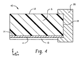
図4はビューイングパネル42の一部の断面を示す図である。ビューイングパネル42は外面12および内面14を含む基材6および基材の表面に隣接する導電性コーティング4を含むことができる。導電性コーティング4は、基材6の表面12、14に直接適用することができる。ビューイングパネル2は、導電性フレーム20に接することができる。導電性フレーム20は、導電性コーティング4と電気的に連絡することができる。導電性フレーム20は、ビューイングパネル42の基材6の外面12の一部に沿って延在することができる。導電性フレーム20は、ビューイングパネル42の基材6の内面14の一部に沿って延在することができる。導電性フレーム20は、ビューイングパネル42の外周縁18に接することができる。導電性フレーム20は、ビューイングパネル42の外周縁全体18に沿って延在することができ、そのため、ビューイングパネル42を取り囲むことができる(例えば、ビューイングパネル42の外周縁全体18に沿って延在することができ、基材の一部および/または導電性コーティング4の一部に沿って延在することができる)。保護材料10は、基材6の表面12、14に隣接して配置することができる。保護材料10は、基材6の表面12、14上に配置することができる。保護材料10は、導電性コーティング4に隣接して配置することができる。保護材料10は、導電性コーティング4の表面の一部に沿って配置することができる。ビューイングパネル42は、導電性コーティング4と導電性フレーム20の間で電気接続性を提供することができる任意の機械的または化学的アタッチメントを使用して導電性フレーム20に連結させることができる(例えば、導電性接着剤、留め具、摩擦嵌合(frictional fit))。基材6は、導電性フレーム20上に射出成形させることができ、導電性コーティング4は、ビューイングパネル42の表面に適用することができる。導電性フレーム20は、少なくとも1つの次元、例えば、d軸次元に沿って、導電性コーティング4に接することができる。導電性フレーム20は、2次元、例えば、d軸次元およびw軸次元に沿って、導電性コーティング4に接することができる。導電性フレーム20は、3次元、例えば、d軸次元、w軸次元、およびh軸次元に沿って、導電性コーティング4に接することができる。
FIG. 4 is a view showing a cross section of a part of the viewing panel 42. The viewing panel 42 can include a substrate 6 including an
図5は、ビューイングパネル52の断面を示す図である。ビューイングパネル52は、基材6および導電性コーティング4を有することができる。ビューイングパネル52はh軸次元に沿って測定される、高さHを有することができる。ビューイングパネル52は、w軸次元に沿って測定される幅Wを有することができる。ビューイングパネル52は、d軸次元に沿って測定される奥行きDを有することができる。導電性コーティング4は、基材の表面6に隣接することができる。ビューイングパネル52は、縁に沿って曲げることができ、そのため、ビューイングパネル2は少なくとも1つの軸に沿って非対称であり、例えば、中心線24について非対称である。基材6および導電性コーティング4上の曲縁26は、導電性フレーム20と導電性コーティング4の間の電気的連絡に対してより大きな面積を提供することができる。導電性コーティング4は、基材6の幅Wの一部にわたって分散させることができる。導電性コーティング4は、基材6の幅W全体にわたって分散させることができる。導電性コーティング4は、基材6の高さHの一部にわたって分散させることができる。導電性コーティング4は、基材6の高さH全体にわたって分散させることができる。
FIG. 5 is a view showing a cross section of the
図7は本明細書で記載されるビューイングパネル82を有する電子レンジドア80を示す図である。本明細書で開示されるビューイングパネル2、22、32、42、52のいずれも、図7の電子レンジドア80と共に使用することができることが理解されるべきである。
FIG. 7 is a diagram illustrating a microwave door 80 having a
基材は任意の形成プロセス、例えば、ポリマ形成プロセスにより形成させることができる。基材は透明材料、例えば、ガラスまたはポリマ基材を含むことができる。例えば、基材は、押出加工、カレンダー加工(calendaring)、成形(例えば、射出成形)、熱成形、真空成形、または他の望ましい形成プロセスにより形成させることができる。基材は平面シートとして製造することができる。基材は、湾曲して形成させることができる。基材は、平面ではないように形成させることができる。基材は、基材の高さ寸法および幅寸法により規定される平面と同一平面内にないように形成させることができる。基材は、湾曲形状で形成させることができ、そのため、奥行き寸法は基材の最大厚さを超える(例えば、基材の厚さは製造の不完全性、例えば、ツール公差、温度などのプロセス条件の変動、冷却下での収縮の変動、などのために変動し得ることが認められる)。基材は、基材の一部が、パネルの平均厚さの2倍以上の奥行き寸法を有するように、湾曲させることができる。基材は、基材の重心で測定される基材の奥行きが、基材の外周に沿ったある点で測定される基材の奥行きより大きくなるように、湾曲させることができる。基材は、基材の奥行き寸法が、基材の重心で最も大きくなるように湾曲させることができる。 The substrate can be formed by any forming process, such as a polymer forming process. The substrate can comprise a transparent material, such as a glass or polymer substrate. For example, the substrate can be formed by extrusion, calendering, molding (eg, injection molding), thermoforming, vacuum forming, or other desired forming processes. The substrate can be manufactured as a flat sheet. The substrate can be formed to be curved. The substrate can be formed so that it is not planar. The substrate can be formed so that it is not in the same plane as the plane defined by the height and width dimensions of the substrate. The substrate can be formed in a curved shape so that the depth dimension exceeds the maximum thickness of the substrate (eg, the substrate thickness is a process such as manufacturing imperfections, eg tool tolerance, temperature, etc. It is recognized that it can vary due to variations in conditions, variations in shrinkage under cooling, etc.). The substrate can be curved so that a portion of the substrate has a depth dimension that is more than twice the average thickness of the panel. The substrate can be curved such that the depth of the substrate measured at the center of gravity of the substrate is greater than the depth of the substrate measured at a point along the circumference of the substrate. The substrate can be curved so that the depth dimension of the substrate is greatest at the center of gravity of the substrate.
導電性コーティングを有するフィルムは、基材の表面上に層化させることができ、ビューイングパネルが形成される。導電性コーティングは、基材の表面に直接適用することができ、ビューイングパネルが形成される。一実施形態では、導電性コーティングを含むフィルムは、金型に入れることができ、ポリマ基材はフィルムの表面に対して射出成形することができ、ビューイングパネルが形成される。一実施形態では、導電性コーティングを含むフィルムは、基材(例えば、ポリマ基材)上に層化させることができ、フィルムおよび基材は熱成形させて、ビューイングパネルにすることができる。フィルムは、これに付着された導電性コーティングの追加の層を有することができる。例えば、フィルムは、1以上の導電性コーティング層を有することができ、例えば、フィルムは、2以上の導電層、例えば、3以上の導電性コーティング層、例えば、5以上の導電性コーティング層、例えば、10以上の導電性コーティング層、例えば、15以上の導電性コーティング層を有することができる。 A film having a conductive coating can be layered on the surface of the substrate to form a viewing panel. The conductive coating can be applied directly to the surface of the substrate, forming a viewing panel. In one embodiment, the film containing the conductive coating can be placed in a mold and the polymer substrate can be injection molded against the surface of the film to form a viewing panel. In one embodiment, a film comprising a conductive coating can be layered on a substrate (eg, a polymer substrate), and the film and substrate can be thermoformed into a viewing panel. The film can have an additional layer of conductive coating attached thereto. For example, a film can have one or more conductive coating layers, for example, a film can have two or more conductive layers, such as three or more conductive coating layers, such as five or more conductive coating layers. It can have 10 or more conductive coating layers, for example, 15 or more conductive coating layers.
基材の外周形状は任意の形状、例えば、円形、楕円、または直線または曲線縁を有する多角形の形状とすることができる。 The outer peripheral shape of the substrate can be any shape, for example, a circle, an ellipse, or a polygon having a straight or curved edge.
フィルムは、熱成形、真空成形、または同様のプロセスを用いて形成された基材に接着させることができる。フィルムは接着促進剤を含むことができる。フィルムは、基材に接着剤を用いて接着させることができる。導電性コーティングは、任意の好適な湿式コーティング技術を用いて、基材またはフィルムに適用することができる。例えば、導電性コーティングは、スクリーン印刷、スプレッディング、スプレーコーティング、スピンコーティング、浸漬、などを用いて適用することができる。一実施形態では、基材は射出成形して、基材の厚さを超える奥行き寸法を有する形状にすることができ、導電性コーティングは、基材の表面に適用することができる。一実施形態では、導電性コーティングは、平面フィルムに適用することができ、平面フィルムおよび基材は、フィルムおよび基材を、全厚(例えば、フィルム、コーティング、および基材の合わせた厚さ)を超える奥行き寸法を有するビューイングパネルに形成することができる熱成形ツール内に配置することができる。 The film can be adhered to a substrate formed using thermoforming, vacuum forming, or similar processes. The film can include an adhesion promoter. The film can be adhered to the substrate using an adhesive. The conductive coating can be applied to the substrate or film using any suitable wet coating technique. For example, the conductive coating can be applied using screen printing, spreading, spray coating, spin coating, dipping, and the like. In one embodiment, the substrate can be injection molded into a shape having a depth dimension that exceeds the thickness of the substrate, and the conductive coating can be applied to the surface of the substrate. In one embodiment, the conductive coating can be applied to a planar film, where the planar film and substrate are the entire thickness of the film and substrate (eg, the combined thickness of the film, coating, and substrate). Can be placed in a thermoforming tool that can be formed into a viewing panel having a depth dimension greater than.
導電性コーティングは、導電性ナノ粒子、導電性金属ナノワイヤ、炭素同素体、例えば炭素ナノチューブ、グラフェン、など、および前記の少なくとも1つを含む組み合わせを含む導電性ナノ粒子から形成させることができる。金属ナノ粒子は銅および銀ナノ粒子を含むことができる。規則正しいネットワークを有する金属メッシュフィルムを使用することができる。透過率は約70から約80%とすることができ、オーム/スクウェアで測定される抵抗は0.5未満とすることができる。導電性コーティングは、導電性トレースおよび透明なセル、すなわち、ほとんどナノ粒子を有さない空隙のパターニングネットワークに形成される導電性金属ナノ粒子から形成させることができる。ネットワークは、ランダムまたは規則正しい形状とすることができ、透過率は約70%とすることができ、抵抗は0.05オーム/スクウェア未満とすることができる。透明なセルは、1ミリメートル(mm)未満、例えば、0.5mm未満、例えば、0.25mm未満のサイズを有することができる。透明な導電性コーティングは、例えば、米国特許第7,601,406号に記載される。 The conductive coating can be formed from conductive nanoparticles comprising conductive nanoparticles, conductive metal nanowires, carbon allotropes such as carbon nanotubes, graphene, and the like, and combinations comprising at least one of the foregoing. The metal nanoparticles can include copper and silver nanoparticles. A metal mesh film with a regular network can be used. The transmission can be about 70 to about 80%, and the resistance measured in ohms / square can be less than 0.5. The conductive coating can be formed from conductive metal nanoparticles formed in conductive traces and transparent cells, i.e., a voided patterning network with few nanoparticles. The network can be random or regular in shape, the transmission can be about 70%, and the resistance can be less than 0.05 ohm / square. Transparent cells can have a size of less than 1 millimeter (mm), such as less than 0.5 mm, such as less than 0.25 mm. Transparent conductive coatings are described, for example, in US Pat. No. 7,601,406.
導電性コーティング(例えば、導電性金属ナノ粒子層)は、いくつかの技術、例えば、導電性インクの印刷(例えば、フレキソ印刷、スクリーン印刷、インクジェット、グラビア印刷)、例えば、銀粒子に還元させることができるハロゲン化銀エマルジョンのコーティングおよびパターニング、導電性ナノワイヤ分散物のコーティング、および銀ナノ粒子分散物またはエマルジョンの自己組織化により、基材に適用することができる。 Conductive coatings (eg, conductive metal nanoparticle layers) can be reduced to several techniques, eg, conductive ink printing (eg, flexographic printing, screen printing, ink jet, gravure printing), eg, silver particles. Can be applied to the substrate by coating and patterning of silver halide emulsions, coating of conductive nanowire dispersions, and self-assembly of silver nanoparticle dispersions or emulsions.
導電性コーティングはEMIシールド材料を含むことができる。導電性コーティングは、純粋な金属、例えば銀(Ag)、ニッケル(Ni)、銅(Cu)、または同様のシールド金属、その金属酸化物、前記の少なくとも1つを含む組み合わせ、および前記の少なくとも1つを含む金属合金、あるいは米国特許第5,476,535号において記載される冶金化学プロセス(MCP)により生成される金属または金属合金を含むことができる。導電性コーティングの金属粒子はナノメートルサイズとすることができ、例えば、例として、粒子の90%は、100ナノメートル(nm)未満の球相当径を有することができる。導電性コーティングの金属は、これが適用される基材表面上の開口を規定する相互に連結された金属トレースのネットワークを形成することができる。導電性コーティングの表面抵抗は1.0オーム/スクエア(オーム/sq)以下とすることができる。導電性コーティングは、ASTM D4935によって決定すると、30メガヘルツ(MHz)から1.5ギガヘルツ(GHz)に対し、25デシベル(dB)を超える、例えば、30dBから80dB、または、40dBから80dBのEMIシールド効果を有することができる。導電性コーティングはネットワーク状に配列された炭素系粒子、例えば、金属メッシュを有する炭素系粒子を含むことができる。炭素系粒子を含む導電性コーティングは、規則正しいネットワーク状に配列することができる。炭素系粒子を含む導電性コーティングは不規則ネットワーク状に配列させることができる。炭素系粒子は、グラフェン、炭素ナノチューブ、または、前記の少なくとも1つを含む組み合わせを含むことができる。 The conductive coating can include an EMI shielding material. The conductive coating may be a pure metal, such as silver (Ag), nickel (Ni), copper (Cu), or similar shielding metal, its metal oxide, a combination comprising at least one of the above, and at least one of the above Or metal or metal alloys produced by the metallurgical chemical process (MCP) described in US Pat. No. 5,476,535. The metal particles of the conductive coating can be nanometer sized, for example, by way of example, 90% of the particles can have a sphere equivalent diameter of less than 100 nanometers (nm). The metal of the conductive coating can form a network of interconnected metal traces that define openings on the substrate surface to which it is applied. The surface resistance of the conductive coating can be 1.0 ohm / square (ohm / sq) or less. Conductive coatings, as determined by ASTM D4935, have an EMI shielding effect of over 30 decibels (dB), for example 30 dB to 80 dB, or 40 dB to 80 dB, for 30 megahertz (MHz) to 1.5 gigahertz (GHz) Can have. The conductive coating may include carbon-based particles arranged in a network, for example, carbon-based particles having a metal mesh. Conductive coatings containing carbon-based particles can be arranged in a regular network. Conductive coatings containing carbon-based particles can be arranged in an irregular network. The carbon-based particles can include graphene, carbon nanotubes, or a combination including at least one of the above.
基材は、ガラス基材とすることができる。基材は、透明なポリマ基材とすることができ、この場合、透明なポリマ基材は熱可塑性樹脂、熱硬化性樹脂、または、前記の少なくとも1つを含む組み合わせを含むことができる。透明なポリマ基材および基材に連結されたフィルムは、同じポリマ材料を含むことができ、または異なるポリマ材料を含むことができる。 The substrate can be a glass substrate. The substrate can be a transparent polymer substrate, in which case the transparent polymer substrate can comprise a thermoplastic resin, a thermosetting resin, or a combination comprising at least one of the foregoing. The transparent polymer substrate and the film coupled to the substrate can comprise the same polymer material or can comprise different polymer materials.
可能な熱可塑性樹脂としては下記が挙げられるが、それらに限定されない:オリゴマ、ポリマ、イオノマ、デンドリマ、コポリマ、例えばグラフトコポリマ、ブロックコポリマ(例えば、スターブロックコポリマ、ランダムコポリマ、など)または、前記の少なくとも1つを含む組み合わせ。そのような熱可塑性樹脂の例としては下記が挙げられるが、それらに限定されない:ポリカーボネート(例えば、ポリカーボネートのブレンド(例えば、ポリカーボネート−ポリブタジエンブレンド、コポリエステルポリカーボネート))、ポリスチレン(例えば、ポリカーボネートおよびスチレンのコポリマ、ポリフェニレンエーテル−ポリスチレンブレンド)、ポリイミド(例えば、ポリエーテルイミド)、アクリロニトリル−スチレン−ブタジエン(ABS)、ポリアリレート、ポリアルキルメタクリレート(例えば、ポリメチルメタクリレート(PMMA))、ポリエステル(例えば、コポリエステル、ポリチオエステル)、ポリオレフィン(例えば、ポリプロピレン(PP)およびポリエチレン、高密度ポリエチレン(HDPE)、低密度ポリエチレン(LDPE)、直鎖状低密度ポリエチレン(LLDPE))、ポリアミド(例えば、ポリアミドイミド)、ポリアリレート、ポリスルホン(例えば、ポリアリールスルホン、ポリスルホンアミド)、ポリフェニレンスルフィド、ポリテトラフルオロエチレン、ポリエーテル(例えば、ポリエーテルケトン(PEK)、ポリエーテルエーテルケトン(PEEK)、ポリエーテルスルホン(PES))、ポリアクリル、ポリアセタール、ポリベンゾキサゾール(例えば、ポリベンゾチアジノフェノチアジン、ポリベンゾチアゾール)、ポリオキサジアゾール、ポリピラジノキノキサリン、ポリピロメリトイミド、ポリキノキサリン、ポリベンズイミダゾール、ポリオキシインドール、ポリオキソイソインドリン(例えば、ポリジオキソイソインドリン)、ポリトリアジン、ポリピリダジン、ポリピペラジン、ポリピリジン、ポリピペリジン、ポリトリアゾール、ポリピラゾール、ポリピロリドン、ポリカルボラン、ポリオキサビシクロノナン、ポリジベンゾフラン、ポリフタルアミド、ポリアセタール、ポリ無水物、ポリビニル(例えば、ポリビニルエーテル、ポリビニルチオエーテル、ポリビニルアルコール、ポリビニルケトン、ポリハロゲン化ビニル、ポリビニルニトリル、ポリビニルエステル、ポリ塩化ビニル)、ポリスルホネート、ポリスルフィド、ポリ尿素、ポリフォスファゼン、ポリシラザン、ポリシロキサン、フルオロポリマ(例えば、ポリフッ化ビニル(PVF)、ポリフッ化ビニリデン(PVDF)、ポリフッ化ビニル(PVF)、フッ素化エチレン−プロピレン(FEP)、ポリエチレンテトラフルオロエチレン(ETFE))または、前記の少なくとも1つを含む組み合わせ。 Possible thermoplastic resins include, but are not limited to: oligomers, polymers, ionomers, dendrimers, copolymers, such as graft copolymers, block copolymers (eg, star block copolymers, random copolymers, etc.) or the aforementioned A combination comprising at least one. Examples of such thermoplastic resins include, but are not limited to: polycarbonate (eg, a blend of polycarbonate (eg, polycarbonate-polybutadiene blend, copolyester polycarbonate)), polystyrene (eg, of polycarbonate and styrene). Copolymer, polyphenylene ether-polystyrene blend), polyimide (eg, polyetherimide), acrylonitrile-styrene-butadiene (ABS), polyarylate, polyalkyl methacrylate (eg, polymethyl methacrylate (PMMA)), polyester (eg, copolyester) , Polythioesters), polyolefins (eg, polypropylene (PP) and polyethylene, high density polyethylene (HDPE) Low density polyethylene (LDPE), linear low density polyethylene (LLDPE)), polyamide (eg, polyamideimide), polyarylate, polysulfone (eg, polyarylsulfone, polysulfonamide), polyphenylene sulfide, polytetrafluoroethylene, poly Ethers (eg, polyetherketone (PEK), polyetheretherketone (PEEK), polyethersulfone (PES)), polyacryl, polyacetal, polybenzoxazole (eg, polybenzothiazinophenothiazine, polybenzothiazole), Polyoxadiazole, polypyrazinoquinoxaline, polypyromellitimide, polyquinoxaline, polybenzimidazole, polyoxyindole, polyoxoisoindoline (eg Dioxoisoindoline), polytriazine, polypyridazine, polypiperazine, polypyridine, polypiperidine, polytriazole, polypyrazole, polypyrrolidone, polycarborane, polyoxabicyclononane, polydibenzofuran, polyphthalamide, polyacetal, polyanhydride, Polyvinyl (eg, polyvinyl ether, polyvinyl thioether, polyvinyl alcohol, polyvinyl ketone, polyhalogenated vinyl, polyvinyl nitrile, polyvinyl ester, polyvinyl chloride), polysulfonate, polysulfide, polyurea, polyphosphazene, polysilazane, polysiloxane, fluoro Polymer (eg, polyvinyl fluoride (PVF), polyvinylidene fluoride (PVDF), polyvinyl fluoride (PVF), fluorinated ethylene Len-propylene (FEP), polyethylene tetrafluoroethylene (ETFE)) or a combination comprising at least one of the foregoing.
より特定的には、熱可塑性樹脂としては、下記が挙げられるが、それらに限定されない:ポリカーボネート樹脂(例えば、レキサン(Lexan)(商標)樹脂、SABICイノベーティブプラスチックス事業(SABIC’s Innovative Plastics business)から市販)、ポリフェニレンエーテル−ポリスチレン樹脂(例えば、ノリル(Noryl)(商標)樹脂、SABICイノベーティブプラスチックス事業から市販)、ポリエーテルイミド樹脂(例えば、ウルテム(Ultem)(商標)樹脂、SABICイノベーティブプラスチックス事業から市販)、ポリブチレンテレフタレート−ポリカーボネート樹脂(例えば、キセノイ(Xenoy)(商標)樹脂、SABICイノベーティブプラスチックス事業から市販)、コポリエステルカーボネート樹脂(例えば、レキサン(商標)SLX樹脂、SABICイノベーティブプラスチックス事業から市販)、または、前記樹脂の少なくとも1つを含む組み合わせ。さらにいっそう特定的には、熱可塑性樹脂としては下記が挙げられるが、それらに限定されない:ポリカーボネート、ポリエステル、ポリアクリレート、ポリアミド、ポリエーテルイミド、ポリフェニレンエーテルのホモポリマおよびコポリマ、または、前記樹脂の少なくとも1つを含む組み合わせ。ポリカーボネートは、ポリカーボネートのコポリマ(例えば、ポリカーボネート−ポリシロキサン、例えばポリカーボネート−ポリシロキサンブロックコポリマ)、直鎖状ポリカーボネート、分枝ポリカーボネート、エンドキャップされたポリカーボネート(例えば、ニトリルによりエンドキャップされたポリカーボネート)、または、前記の少なくとも1つを含む組み合わせ、例えば、分枝および直鎖状ポリカーボネートの組み合わせを含むことができる。 More specifically, thermoplastic resins include, but are not limited to, polycarbonate resins (eg, Lexan ™ resin, SABIC's Innovative Plastics business). ), Polyphenylene ether-polystyrene resin (eg, Noryl ™ resin, commercially available from SABIC Innovative Plastics), polyetherimide resin (eg, Ultem ™ resin, SABIC Innovative Plastics) Commercially available), polybutylene terephthalate-polycarbonate resins (eg, Xenoy ™ resin, SABIC Innovative Plastics) Commercially available from business), copolyestercarbonate resins (e.g., Lexan (TM) SLX resin, commercially available from SABIC Innovative Plastics business), or a combination comprising at least one of the resin. More specifically, thermoplastic resins include, but are not limited to: polycarbonates, polyesters, polyacrylates, polyamides, polyetherimides, polyphenylene ether homopolymers and copolymers, or at least one of the above resins. Combination including one. Polycarbonates are polycarbonate copolymers (eg, polycarbonate-polysiloxane, eg, polycarbonate-polysiloxane block copolymer), linear polycarbonate, branched polycarbonate, end-capped polycarbonate (eg, nitrile end-capped polycarbonate), or , Combinations comprising at least one of the foregoing, for example, combinations of branched and linear polycarbonates.
ビューイングパネルの透明なポリマ基材および/またはフィルムは、この型のポリマ組成物中に通常組み入れられる様々な添加物を含むことができ、ただし、添加物(複数可)はポリマの所望の特性、特に、透明性、たわみ、応力、および曲げ剛性に著しく悪影響を及ぼさないように選択されるということを条件とする。そのような添加物は、基材および/またはフィルムを形成するための成分の混合中の好適な時間に混合することができる。例示的な添加物としては、衝撃改質剤、フィラー、補強剤、抗酸化剤、熱安定剤、光安定剤、紫外(UV)光安定剤、可塑剤、潤滑剤、離型剤、帯電防止剤、着色剤(例えばカーボンブラックおよび有機染料)、表面効果添加物、放射線安定剤(例えば、赤外線吸収)、難燃剤、および抗ドリップ剤が挙げられる。添加物の組み合わせ、例えば、熱安定剤、離型剤、および紫外線安定剤の組み合わせが、使用され得る。添加物の総量(衝撃改質剤、フィラー、または補強剤以外)は、基材および/またはフィルムの組成物の総重量に基づき、0.001重量パーセント(wt%)から5wt%とすることができる。 The transparent polymer substrate and / or film of the viewing panel can include various additives normally incorporated into this type of polymer composition, provided that the additive (s) are the desired properties of the polymer. In particular, provided that it is selected so as not to significantly affect transparency, deflection, stress, and bending stiffness. Such additives can be mixed at a suitable time during the mixing of the components to form the substrate and / or film. Exemplary additives include impact modifiers, fillers, reinforcing agents, antioxidants, heat stabilizers, light stabilizers, ultraviolet (UV) light stabilizers, plasticizers, lubricants, mold release agents, antistatics. Agents, colorants (eg, carbon black and organic dyes), surface effect additives, radiation stabilizers (eg, infrared absorption), flame retardants, and anti-drip agents. Combinations of additives can be used, for example, a combination of heat stabilizer, mold release agent, and UV stabilizer. The total amount of additives (other than impact modifiers, fillers, or reinforcing agents) may be 0.001 weight percent (wt%) to 5 wt% based on the total weight of the substrate and / or film composition. it can.
基材は、表面エネルギーを変化させる、または、導電性コーティングの接着を増強させるために、物理または化学技術、例えば紫外線(UV)、コロナ、プラズマ、または化学プライマを使用して、前処理することができる。 The substrate is pretreated using physical or chemical techniques such as ultraviolet (UV), corona, plasma, or chemical primers to change the surface energy or enhance adhesion of the conductive coating. Can do.
導電性コーティング(例えば、透明な導電性コーティング)は、電気抵抗を減少させるために、追加の導電性金属層を用いて、メッキすることができる。メッキ技術は、銀および銅などの導電性金属を用いた無電解および電気メッキを含むことができる。メッキ技術は、米国特許第8,105,472号および米国特許公開第2011/0003141号に記載される。 A conductive coating (eg, a transparent conductive coating) can be plated with an additional conductive metal layer to reduce electrical resistance. Plating techniques can include electroless and electroplating using conductive metals such as silver and copper. Plating techniques are described in US Pat. No. 8,105,472 and US Patent Publication No. 2011/0003141.
透明な導電性コーティングが電子レンジの窓アセンブリに含められる場合、コーティングは、窓の外側または内側に配置することができる。透明な導電性コーティングが電子レンジの窓アセンブリに含められる場合、コーティングは多層窓内の1つの層として配置することができ、例えば、導電性ネットワークに対する保護を提供するための2つ以上の透明な基材間に挟まれている。透明な導電性コーティングの単一の層を使用することができ、または複数の層を、任意でそれらの間に空間を配置して使用することができる。透明な導電性コーティングは窓の透明な部分全体を被覆することができる(例えば、100%)。透明な導電性コーティングは、窓の一部(例えば、50%以上)を被覆することができる。透明な導電性コーティングは、電子レンジの金属ドアフレームまたは筐体に接地することができる。コーティングと金属フレームの間の電気的接続は、様々な技術、例えば、限定はされないが導電性インクまたはペースト、銅テープなどの導電性テープ、はんだ付け接続、または導電性接着剤により達成することができる。接続の一端は、電子レンジの金属ドアフレームまたは筐体に付着させることができ、接続の他端は、透明な導電性コーティングに付着させることができる。コーティングへの電気的付着は、外周の周りの複数の位置でまたは連続して実施することができ、導電性ネットワークの全ての部分への十分な接続が提供される。 If a transparent conductive coating is included in the microwave window assembly, the coating can be placed outside or inside the window. If a transparent conductive coating is included in the microwave window assembly, the coating can be arranged as a single layer in a multi-layer window, eg, two or more transparent to provide protection against the conductive network. It is sandwiched between the substrates. A single layer of transparent conductive coating can be used, or multiple layers can be used, optionally with a space between them. A transparent conductive coating can cover the entire transparent portion of the window (eg, 100%). The transparent conductive coating can cover a portion of the window (eg, 50% or more). The transparent conductive coating can be grounded to the metal door frame or housing of the microwave oven. The electrical connection between the coating and the metal frame can be achieved by various techniques such as, but not limited to, conductive inks or pastes, conductive tapes such as copper tape, soldered connections, or conductive adhesives. it can. One end of the connection can be attached to the metal door frame or housing of the microwave oven, and the other end of the connection can be attached to the transparent conductive coating. Electrical attachment to the coating can be performed at multiple locations around the perimeter or sequentially, providing sufficient connectivity to all portions of the conductive network.
ビューイングパネルは、430THzから790THzの周波数を有する入射EMIの50%以上(例えば、50パーセント透過率)、例えば、60%から100%、または、70%から100%を透過させることができる。ビューイングパネルの透明なポリマ、基材、フィルム、および/または材料は、430THzから790THzの周波数を有する入射EMIの50%以上、例えば、75%から100%、または、90%から100%を透過させることができる。実験室スケールサンプルに対するパーセント透過率は、ASTM D1003、手順Bを用い、CIE標準発光体Cを使用して決定することができる。ASTM D−1003(手順B、分光光度計、使用するのは発光体C、拡散照明、一方向観察)は下記としてパーセント透過率を規定する: The viewing panel can transmit 50% or more (eg, 50 percent transmittance) of incident EMI having a frequency from 430 THz to 790 THz, eg, 60% to 100%, or 70% to 100%. The transparent polymer, substrate, film, and / or material of the viewing panel transmits more than 50% of incident EMI having a frequency of 430 THz to 790 THz, for example, 75% to 100%, or 90% to 100% Can be made. The percent transmission for laboratory scale samples can be determined using ASTM D1003, Procedure B and using CIE standard illuminant C. ASTM D-1003 (Procedure B, spectrophotometer, using illuminant C, diffuse illumination, unidirectional observation) defines percent transmission as follows:

Io=入射光の強度。
導電性フレームは、ビューイングパネルの周りに導電性コーティングと電気的に連絡させて配置することができる。導電性フレームと電気的に連絡した導電性コーティングを有するビューイングパネルは、2.2GHzから2.6GHzに対し、垂直偏波および水平偏波の両方について、関係する標準(例えば、国際標準、例えばCISPR11、CISPR19、CISPR13、など、または全国標準、例えばFCCパート18、EN55011、または同様の全国もしくは国際標準)により決定すると、1マイクロボルトに対し30デシベル以上(dBμV)、例えば、30dBμVから75dBμV、または、35dBμVから75dBμVのEMIシールド効果を有することができる。
The conductive frame can be placed in electrical communication with the conductive coating around the viewing panel. Viewing panels having a conductive coating in electrical communication with a conductive frame, for 2.2 GHz to 2.6 GHz, for both vertical and horizontal polarization, are relevant standards (eg international standards such as As determined by CISPR11, CISPR19, CISPR13, etc. or national standards such as
下記実施例は、本明細書で開示されるビューイングパネルを形成する方法およびビューイングパネルの例示にすぎず、この範囲を制限することは意図されない。 The following examples are merely illustrative of methods and viewing panels for forming the viewing panels disclosed herein and are not intended to limit this scope.
実施例1:熱成形サンプル試験
この実施例では、シート熱成形ツールを、2%(サンプル1)、4%(サンプル2)、6%(サンプル3)、8%(サンプル4)、10%(サンプル5)、および12%(サンプル6)の様々な曲げ半径を有する6つのドーム形状サンプルを用いて構築した。使用した熱成形ツールは、ゲイス(GEISS)(商標)AG U8機とした。熱成形プロセスでは、フィルムサンプルを、上部および底部オーブンにより表面の上および下から加熱し、温度センサがフィルムの上および底表面温度をモニタし、熱成形ツールが底部センサにより活性化され、底部フィルム温度がセットポイント(例えば、加工処理温度)に到達すると、底部オーブンは後退し、ツールはフィルムに上がり込み、真空引きし、上部オーブン下でフィルムサンプルを成形させる。簡単に言うと、熱成形中、ツールが機械内に配置され、機械開口部と一列になるように調整され、サンプル(例えば、未成形シート)が、開口プレートとo−リング開口部の間に配置され、サンプルはクランプフレームにより固定され、フィルムは所望の温度まで加熱され、ツールはサンプルに入り込み、真空引きされ、サンプルは成形されてツール形状となる。サンプル中、機械は100%加熱強度で動作された。加工処理時間は各サンプルに対して変動し、フィルムサンプルが設定温度に到達した時に、機械により出力された。
Example 1: Thermoforming Sample Test In this example, a sheet thermoforming tool was tested with 2% (Sample 1), 4% (Sample 2), 6% (Sample 3), 8% (Sample 4), 10% ( Samples 5) and 6 dome-shaped samples with various bend radii of 12% (Sample 6) were constructed. The thermoforming tool used was a GEISS ™ AG U8 machine. In the thermoforming process, film samples are heated from above and below the surface by top and bottom ovens, temperature sensors monitor the top and bottom surface temperatures of the film, thermoforming tools are activated by the bottom sensor, and the bottom film When the temperature reaches a set point (eg, processing temperature), the bottom oven is retracted and the tool is raised into the film and evacuated to form a film sample under the top oven. Briefly, during thermoforming, the tool is placed in the machine and adjusted to align with the machine opening and a sample (eg, an unformed sheet) is placed between the opening plate and the o-ring opening. Once placed, the sample is secured by a clamp frame, the film is heated to the desired temperature, the tool enters the sample, is evacuated, and the sample is molded into a tool shape. During the sample, the machine was operated at 100% heating intensity. Processing time varied for each sample and was output by the machine when the film sample reached the set temperature.
熱成形サンプルでは、ポリエチレンテレフタレート(PET)が基材材料として使用され、使用された導電性コーティングは、0.005オーム毎スクウェア以下の表面抵抗、70%以上の透過率、および3.5%以下のヘイズ値を有する導電性フィルムであった。基材は0.125mmの厚さを有し、導電性コーティングは14マイクロメートル(μm)の厚さを有した。 In thermoformed samples, polyethylene terephthalate (PET) is used as the substrate material, and the conductive coating used is a surface resistance of 0.005 ohms per square or less, a transmittance of 70% or more, and 3.5% or less It was the electroconductive film which has the haze value of. The substrate had a thickness of 0.125 mm and the conductive coating had a thickness of 14 micrometers (μm).
実施例2:EMIシールド試験
この実施例では、サンプル1および6を試験し、金属基材および実施例1で記載されるのと同じ導電性フィルムを有するサンプル7ならびにポリエチレンテレフタレート基材および実施例1で記載されるのと同じ導電性フィルムを有するサンプル8、平面サンプル(すなわち、曲げなし)と比較した。各サンプルにおける基材は0.125mmの厚さとし、一方、導電性コーティングは14μmの厚さとした。サンプルの各々を、ビューイングパネルを形成する電子レンジドアに取り付けた。実施例で使用した電子レンジは、シャープ(SHARP)製の、モデル#RE−TE−W5とし、400mm×365mm×275mmの外寸および300mm×335mm×200mmの内寸、12キログラム(kg)の重量、2.45ギガヘルツ(GHz)の周波数(波長および12.2センチメートル(cm))を有した。この電子レンジに対する電力は500ワットであった。
Example 2: EMI Shield Test In this example,
マイクロ波放射線放出試験(すなわち、電力密度試験)を各サンプルについて、マイクロ波調理機器のためのUL923に従い実施した。この場合、試験を実施する前には、放射線放出は電子レンジドアから5cm以上の位置で1ミリワット毎平方センチメートル(mW/cm2)未満でなければならず、試験中、放出されるマイクロ波放射線は電子レンジドアから5cm以上の位置で5mW/cm2未満でなければならない。内箱負荷は約8.5cmの内径を有する600mLビーカー内の275±15ミリリットル(mL)の室温(例えば、20±5℃)の水道水である。マイクロ波放射線放出をドアを完全に閉めて測定し(密閉試験)および、これを内箱中へのマイクロ波エネルギーの発生が可能となる位置まで開けて測定する(開放試験)。 A microwave radiation emission test (ie, power density test) was performed for each sample in accordance with UL 923 for microwave cooking equipment. In this case, before conducting the test, the radiation emission must be less than 1 milliwatt per square centimeter (mW / cm 2 ) at least 5 cm from the microwave door, and during the test, the emitted microwave radiation is an electron Must be less than 5 mW / cm 2 at 5 cm or more from the range door. The inner box load is 275 ± 15 milliliters (mL) of room temperature (eg, 20 ± 5 ° C.) tap water in a 600 mL beaker having an inner diameter of about 8.5 cm. Microwave radiation emission is measured with the door completely closed (sealing test) and opened to a position where microwave energy can be generated in the inner box (open test).
試験では、開放試験に対する負荷力は開くのに必要な力の1.5倍とし、密閉試験では、閉じるのに必要な力の2.0倍とした。放射線放出を測定するために、プローブをビューイングパネルの中心部分内の電子レンジドアの中心位置の前にセットした。放射線放出を50mmで20秒間測定し、その後、ドアを10mm開き、試験を再び実施した。 In the test, the load force for the open test was 1.5 times the force required to open, and in the sealed test, it was 2.0 times the force required to close. In order to measure radiation emission, the probe was set in front of the center position of the microwave door in the central part of the viewing panel. Radiation emission was measured at 50 mm for 20 seconds, after which the door was opened 10 mm and the test was performed again.
図6はこれらの試験からの結果を示す。サンプル1、6、7、および8を試験し、密閉試験70および開放試験72に対して測定した。図6で見てわかるように、放射線放出(電力密度)をmW/cm2で測定したが、値はサンプル1および6では減少せず、本明細書で開示される透明物品は、金属ドアに比べおよび平面基材に比べ十分なEMIシールドを提供することができることが意味される。値は全てのサンプル間で一致しており、本明細書で開示される透明物品は、電子レンジドア適用において価値を見出すことができることが示され、この場合、透明物品は可視光透過率の増加、マイクロ波放射のための関係する全国および産業標準を満たす十分なマイクロ波シールド能力を提供することができ、パネルの重量およびコストを低減させることができ、改善された美的感覚および曲線設計を可能にするより大きな設計の自由を提供することができる。
FIG. 6 shows the results from these tests.
本明細書で他に特に規定がなければ、標準、規則、試験方法など、例えばASTM D1003、ASTM D4935、ASTM1746、FCCパート18、CISPR11、およびCISPR19へのいずれかの言及は、本願の出願時に効力のある標準、規則、ガイダンスまたは方法を示す。
Unless otherwise specified herein, any reference to standards, rules, test methods, etc., such as ASTM D1003, ASTM D4935, ASTM 1746,
電磁干渉シールドを含む透明物品は少なくとも下記実施形態を含む: A transparent article comprising an electromagnetic interference shield includes at least the following embodiments:
実施形態1:電子レンジのためのビューイングパネルを形成する方法であって、導電性コーティングを含むフィルムを金型に入れ、導電性コーティングを有するフィルムの表面に対して基材を成形させ、ビューイングパネルを形成する工程、あるいは基材を射出成形し、成形後に導電性コーティングを基材の表面に適用し、ビューイングパネルを形成する工程を含み、ここで、基材は、透明なポリマまたはガラスから選択され、導電性コーティングは、ASTM D4935により決定すると、30MHzから3.0GHzに対して25dBを超えるEMIシールド効果を有し、ならびにビューイングパネルは、430THzから790THzの周波数を有する入射光の50%以上の透過率を有する、方法。 Embodiment 1: A method of forming a viewing panel for a microwave oven, wherein a film containing a conductive coating is placed in a mold, a substrate is molded against the surface of the film having the conductive coating, and the view Forming a viewing panel, or injection molding the substrate and applying a conductive coating to the surface of the substrate after molding to form a viewing panel, wherein the substrate is a transparent polymer or The conductive coating selected from glass has an EMI shielding effect greater than 25 dB from 30 MHz to 3.0 GHz as determined by ASTM D4935, and the viewing panel has incident light with a frequency of 430 THz to 790 THz. A method having a transmittance of 50% or more.
実施形態2:電子レンジのためのビューイングパネルを形成する方法であって、導電性コーティングを含むフィルムを基材に連結させ、パネルプリフォームを形成させる工程、ならびにパネルプリフォームを熱成形または真空成形して、ビューイングパネルを形成させる工程を含み、ここで、基材は、透明なポリマまたはガラスから選択され、コーティングは1.0オーム/sq以下の表面抵抗を有し、ならびにビューイングパネルは、430THzから790THzの周波数を有する入射光の50%以上の透過率を有する、方法。 Embodiment 2: A method for forming a viewing panel for a microwave oven, wherein a film comprising a conductive coating is connected to a substrate to form a panel preform, and the panel preform is thermoformed or vacuumed Forming a viewing panel, wherein the substrate is selected from a transparent polymer or glass, the coating has a surface resistance of 1.0 ohm / sq or less, and the viewing panel Is a method having a transmittance of 50% or more of incident light having a frequency of 430 THz to 790 THz.
実施形態3:コーティングは1.0オーム/sq以下の表面抵抗を有する、実施形態1の方法。
Embodiment 3: The method of
実施形態4:コーティングは、ASTM D4935により決定すると、30MHzから3.0GHzに対して25dBを超えるEMIシールド効果を有する、実施形態2の方法。
Embodiment 4: The method of
実施形態5:導電性材料のフレームをビューイングパネルに接合させる工程を含む、実施形態1−4のいずれかの方法。 Embodiment 5: The method of any of Embodiments 1-4, comprising joining a frame of conductive material to the viewing panel.
実施形態6:導電性材料のフレームを金型に導入し、基材をフレームに対して成形する工程を含む、実施形態1または実施形態3の方法。
Embodiment 6: The method of
実施形態7:導電性材料のフレームを熱成形ツールまたは真空成形ツールに導入し、パネルプリフォームをフレームに対して熱成形または真空成形する工程を含む、実施形態2、4、または5のいずれかの方法。
Embodiment 7: Any of
実施形態8:保護材料を導電性コーティングに適用する工程を含み、保護材料は、液状塗料、保護フィルム、またはガラスから選択される、実施形態1−7のいずれかの方法。 Embodiment 8: The method of any of Embodiments 1-7, comprising applying a protective material to the conductive coating, wherein the protective material is selected from a liquid paint, a protective film, or glass.
実施形態9:パネルをトリミングする工程含む、実施形態1−8のいずれかの方法。 Embodiment 9: The method of any of Embodiments 1-8, comprising the step of trimming the panel.
実施形態10:ビューイングパネルは高さ寸法および幅寸法により規定される平面と同一平面内にないような形状とされる、実施形態1−9のいずれかの方法。
実施形態11:ビューイングパネルは、奥行き寸法がパネルの最大厚さを超えるような湾曲形状を有する、実施形態1−9のいずれかの方法。 Embodiment 11: The method of any of Embodiments 1-9, wherein the viewing panel has a curved shape such that the depth dimension exceeds the maximum thickness of the panel.
実施形態12:ビューイングパネルの一部は、パネルの平均厚さの2倍以上の奥行き寸法を有する、実施形態1−10のいずれかの方法。 Embodiment 12: The method of any of embodiments 1-10, wherein a portion of the viewing panel has a depth dimension that is greater than or equal to twice the average thickness of the panel.
実施形態13:パネルの中心で測定されるパネルの中心奥行きは、パネルの外周で測定される縁奥行きより大きい、実施形態1−11のいずれかの方法。 Embodiment 13: The method of any of embodiments 1-11, wherein the center depth of the panel measured at the center of the panel is greater than the edge depth measured at the perimeter of the panel.
実施形態14:ビューイングパネルの奥行き寸法は、ビューイングパネルの重心で最も大きい、実施形態1−12のいずれかの方法。 Embodiment 14: The method of any of Embodiments 1-12, wherein the depth dimension of the viewing panel is largest at the center of gravity of the viewing panel.
実施形態15:電子レンジのためのビューイングパネルであって、透明なポリマまたはガラスを含む基材と、基材の表面に隣接する導電性コーティングとを備え、ここで、コーティングは、導電性ナノ粒子、導電性金属ナノワイヤ、炭素同素体、または、前記の少なくとも1つを含む組み合わせから選択される導電性ナノ粒子を含み、導電性ナノ粒子はネットワーク状に配列され、ビューイングパネルは、430THzから790THzの周波数を有する入射光の50%以上の透過率を有し、ならびに、ビューイングパネルは、ASTM D4935により決定すると、30MHzから3.0GHzに対して25dBを超えるEMIシールド効果を有する、ビューイングパネル。 Embodiment 15 A viewing panel for a microwave oven comprising a substrate comprising a transparent polymer or glass and a conductive coating adjacent to the surface of the substrate, wherein the coating comprises conductive nano Including conductive nanoparticles selected from particles, conductive metal nanowires, carbon allotropes, or combinations comprising at least one of the foregoing, wherein the conductive nanoparticles are arranged in a network, and the viewing panel is from 430 THz to 790 THz A viewing panel having an EMI shielding effect of greater than 25 dB for 30 MHz to 3.0 GHz as determined by ASTM D4935 .
実施形態16:コーティングは、1.0オーム/sq以下の表面抵抗を有する、実施形態15のビューイングパネル。 Embodiment 16: The viewing panel of embodiment 15, wherein the coating has a surface resistance of 1.0 ohm / sq or less.
実施形態17:導電性コーティングは直接、基材に連結される、実施形態15または実施形態16のビューイングパネル。
Embodiment 17: The viewing panel of embodiment 15 or
実施形態18:導電性コーティングは、フィルムに接着され、フィルムは基材に連結される、実施形態15または実施形態16のビューイングパネル。
Embodiment 18: The viewing panel of embodiment 15 or
実施形態19:導電性コーティングに隣接する保護材料を含み、保護材料は、液状塗料、保護フィルム、またはガラスから選択される、実施形態15−18のいずれかのビューイングパネル。 Embodiment 19 The viewing panel of any of embodiments 15-18, comprising a protective material adjacent to the conductive coating, wherein the protective material is selected from a liquid paint, a protective film, or glass.
実施形態20:ビューイングパネルは高さ寸法および幅寸法により規定される平面と同一平面内にないような形状とされる、実施形態15−19のいずれかの方法。
実施形態21:ビューイングパネルは、奥行き寸法がパネルの最大厚さを超えるような湾曲形状を有する、実施形態15−20のいずれかのビューイングパネル。 Embodiment 21: The viewing panel of any of embodiments 15-20, wherein the viewing panel has a curved shape such that the depth dimension exceeds the maximum thickness of the panel.
実施形態22:ビューイングパネルの一部は、パネルの平均厚さの2倍以上の奥行き寸法を有する、実施形態15−21のいずれかのビューイングパネル。
実施形態23:パネルの中心で測定されるパネルの中心奥行きは、パネルの外周で測定される縁奥行きより大きい、実施形態15−22のいずれかのビューイングパネル。 Embodiment 23: The viewing panel of any of embodiments 15-22, wherein the center depth of the panel measured at the center of the panel is greater than the edge depth measured at the perimeter of the panel.
実施形態24:ビューイングパネルの奥行き寸法は、ビューイングパネルの重心で最も大きい、実施形態15−23のいずれかのビューイングパネル。 Embodiment 24: The viewing panel of any of embodiments 15-23, wherein the depth dimension of the viewing panel is largest at the center of gravity of the viewing panel.
実施形態25:実施形態1−24のいずれかのビューイングパネルを含む電子レンジドア。 Embodiment 25: A microwave oven door including the viewing panel of any of Embodiments 1-24.
一般に、発明は、代替的に、本明細書で開示される任意の適切な構成要素を含む、これらから構成される、またはこれらから本質的に構成され得る。発明は加えて、またはその代わりに、先行技術組成物で使用される、または、そうでなければ、本発明の機能および/または目的の達成に必要でない任意の構成要素、材料、材料成分、アジュバントまたは種を欠く、または実質的に含まないように策定することができる。 In general, the invention may alternatively comprise, consist of, or consist essentially of any suitable component disclosed herein. The invention is in addition to or instead of any component, material, material component, adjuvant used in prior art compositions or otherwise not necessary to achieve the functions and / or objectives of the present invention. Or it can be formulated to be lacking or substantially free of species.
本明細書で開示される全ての範囲は終点を含み、終点は独立して互いに組み合わせ可能である(例えば、「25wt%まで、または、より特定的には、5wt%から20wt%」の範囲は、終点および「5wt%から25wt%」の範囲の全ての中間値を含む、など)。「組み合わせ」は、ブレンド、混合物、合金、反応生成物、などを含む。さらに、「第1の」「第2の」などの用語は、本明細書ではいずれの順、量、または重要性も示さないが、むしろ、1つの要素を別の要素と比較して示すために使用される。「1つの(a、an)」および「その(the)」という用語は本明細書では、量の制限を示さず、本明細書で別記されない限り、または文脈により明確に反対されない限り、単数形および複数形の両方を含むと解釈されるべきである。添え字「(複数可)」は、本明細書では、これが修飾する用語の単数形および複数形の両方を含むことが意図され、よって、1つ以上のその用語を含む(例えば、フィルム(複数可)は1つ以上のフィルムを含む)。明細書を通して、「1つの実施形態」、「別の実施形態」、「一実施形態」、などへの言及は、実施形態に関連して記載される特定の要素(例えば、特徴、構造、および/または特性)が、本明細書で記載される少なくとも1つの実施形態に包含され、他の実施形態では存在してもよく、または存在しなくてもよいことを意味する。加えて、記載される要素は、様々な実施形態において任意の好適な様式で組み合わせることができることが理解されるべきである。 All ranges disclosed herein include endpoints and the endpoints can be independently combined with each other (eg, a range of “up to 25 wt%, or more specifically 5 wt% to 20 wt%” Endpoints and include all intermediate values in the range of “5 wt% to 25 wt%”, etc.). “Combination” includes blends, mixtures, alloys, reaction products, and the like. Furthermore, terms such as “first”, “second” do not indicate any order, amount, or importance herein, but rather to indicate one element as compared to another. Used for. The terms “a (an)” and “the” herein do not imply a limit on the amount, and unless stated otherwise herein or otherwise clearly contradicted by context, And should be construed to include both plural forms. The subscript “(s)” is intended herein to include both the singular and plural terms of which it modifies, and thus includes one or more of that term (eg, film (s) Yes) includes one or more films). Throughout the specification, references to “one embodiment,” “another embodiment,” “one embodiment,” and the like refer to particular elements (eg, features, structures, and Is included in at least one embodiment described herein and may or may not be present in other embodiments. In addition, it is to be understood that the described elements can be combined in any suitable manner in the various embodiments.
特定の実施形態について記載してきたが、現在のところ予期されないまたは予期され得ない代替案、改変、変更、改善および実質的な等価物は、出願人または他の当業者であれば思いつくことができる。したがって、出願された、および補正される可能性のある添付の特許請求の範囲は、そのような代替案、改変、変更、改善および実質的な等価物を全て包含することが意図される。 While specific embodiments have been described, alternatives, modifications, changes, improvements and substantial equivalents that are not currently or unexpectedly anticipated can be conceived by the applicant or other person skilled in the art. . Accordingly, the appended claims as filed and subject to amendment are intended to embrace all such alternatives, modifications, variations, improvements and substantial equivalents.
Claims (20)
導電性コーティングを含むフィルムを金型に入れ、前記導電性コーティングを有する前記フィルムの表面に対して基材を成形させ、前記ビューイングパネルを形成する工程、あるいは
基材を射出成形し、成形後に導電性コーティングを前記基材の表面に適用し、前記ビューイングパネルを形成する工程、
を含み、
前記基材は、透明なポリマまたはガラスから選択され、
前記導電性コーティングは、ASTM D4935により決定すると、30MHzから3.0GHzに対して25dBを超えるEMIシールド効果を有し、ならびに
前記ビューイングパネルは、430THzから790THzの周波数を有する入射光の50%以上の透過率を有する、方法。 A method of forming a viewing panel for a microwave oven, comprising:
A film containing a conductive coating is placed in a mold, a base is formed on the surface of the film having the conductive coating, and the viewing panel is formed, or the base is injection-molded, and after molding Applying a conductive coating to the surface of the substrate to form the viewing panel;
Including
The substrate is selected from a transparent polymer or glass;
The conductive coating has an EMI shielding effect of more than 25 dB from 30 MHz to 3.0 GHz as determined by ASTM D4935, and the viewing panel has more than 50% of incident light having a frequency of 430 THz to 790 THz Having a transmittance of.
導電性コーティングを含むフィルムを基材に連結させ、パネルプリフォームを形成させる工程、ならびに
前記パネルプリフォームを熱成形または真空成形して、前記ビューイングパネルを形成させる工程、
を含み、
前記基材は、透明なポリマまたはガラスから選択され、
前記コーティングは1.0オーム/sq以下の表面抵抗を有し、ならびに
前記ビューイングパネルは、430THzから790THzの周波数を有する入射光の50%以上の透過率を有する、方法。 A method of forming a viewing panel for a microwave oven, comprising:
Connecting a film containing a conductive coating to a substrate to form a panel preform, and thermoforming or vacuum forming the panel preform to form the viewing panel;
Including
The substrate is selected from a transparent polymer or glass;
The method wherein the coating has a surface resistance of 1.0 ohm / sq or less, and the viewing panel has a transmittance of 50% or more of incident light having a frequency of 430 THz to 790 THz.
透明なポリマまたはガラスを含む基材と、
前記基材の表面に隣接する導電性コーティングと
を含み、
前記コーティングは、導電性ナノ粒子、導電性金属ナノワイヤ、炭素同素体、または、前記の少なくとも1つを含む組み合わせから選択される導電性ナノ粒子を含み、前記導電性ナノ粒子はネットワーク状に配列され、
前記ビューイングパネルは、430THzから790THzの周波数を有する入射光の50%以上の透過率を有し、ならびに
前記ビューイングパネルは、ASTM D4935により決定すると、30MHzから3.0GHzに対して25dBを超えるEMIシールド効果を有する、ビューイングパネル。 A viewing panel for a microwave oven,
A substrate comprising a transparent polymer or glass;
A conductive coating adjacent to the surface of the substrate;
The coating includes conductive nanoparticles selected from conductive nanoparticles, conductive metal nanowires, carbon allotropes, or a combination comprising at least one of the above, and the conductive nanoparticles are arranged in a network,
The viewing panel has a transmissivity of 50% or more of incident light having a frequency of 430 THz to 790 THz, and the viewing panel exceeds 25 dB for 30 MHz to 3.0 GHz as determined by ASTM D4935 Viewing panel with EMI shielding effect.
Applications Claiming Priority (3)
| Application Number | Priority Date | Filing Date | Title |
|---|---|---|---|
| US201461969645P | 2014-03-24 | 2014-03-24 | |
| US61/969,645 | 2014-03-24 | ||
| PCT/IB2015/052157 WO2015145355A1 (en) | 2014-03-24 | 2015-03-24 | Transparent articles including electromagnetic radiation shielding |
Publications (2)
| Publication Number | Publication Date |
|---|---|
| JP2017512680A true JP2017512680A (en) | 2017-05-25 |
| JP2017512680A5 JP2017512680A5 (en) | 2018-05-17 |
Family
ID=52824513
Family Applications (1)
| Application Number | Title | Priority Date | Filing Date |
|---|---|---|---|
| JP2016558634A Pending JP2017512680A (en) | 2014-03-24 | 2015-03-24 | Transparent articles including electromagnetic radiation shields |
Country Status (6)
| Country | Link |
|---|---|
| US (1) | US20180220501A1 (en) |
| EP (1) | EP3122805B1 (en) |
| JP (1) | JP2017512680A (en) |
| KR (1) | KR20160135814A (en) |
| CN (1) | CN106103555A (en) |
| WO (1) | WO2015145355A1 (en) |
Families Citing this family (27)
| Publication number | Priority date | Publication date | Assignee | Title |
|---|---|---|---|---|
| WO2015024177A1 (en) | 2013-08-20 | 2015-02-26 | Whirlpool Corporation | Method for detecting the status of popcorn in a microwave |
| JP6368371B2 (en) | 2013-12-23 | 2018-08-01 | ワールプール コーポレイション | Cut-off circuit for radio frequency generator |
| WO2016144872A1 (en) | 2015-03-06 | 2016-09-15 | Whirlpool Corporation | Method of calibrating a high power amplifier for a radio frequency power measurement system |
| US10531524B2 (en) * | 2015-03-09 | 2020-01-07 | Whirlpool Corporation | Microwave oven having door with transparent panel |
| ES2690269T3 (en) * | 2015-03-16 | 2018-11-20 | Martin Christ Gefriertrocknungsanlagen Gmbh | Freeze dryer with a viewing window |
| WO2016196939A1 (en) | 2015-06-03 | 2016-12-08 | Whirlpool Corporation | Method and device for electromagnetic cooking |
| EP3400756B8 (en) | 2016-01-08 | 2020-02-26 | Whirlpool Corporation | Multiple cavity microwave oven insulated divider |
| EP3400755A1 (en) | 2016-01-08 | 2018-11-14 | Whirlpool Corporation | Method and apparatus for determining heating strategies |
| WO2017131698A1 (en) | 2016-01-28 | 2017-08-03 | Whirlpool Corporation | Method and apparatus for delivering radio frequency electromagnetic energy to cook foodstuff |
| US10827570B2 (en) | 2016-02-15 | 2020-11-03 | Whirlpool Corporation | Method and apparatus for delivering radio frequency electromagnetic energy to cook foodstuff |
| KR102451452B1 (en) * | 2016-02-29 | 2022-10-06 | 삼성전자주식회사 | Cooking apparatus |
| EP3551935B1 (en) | 2016-12-06 | 2022-05-25 | Whirlpool Corporation | Microwave oven with full glass door |
| WO2018133021A1 (en) * | 2017-01-20 | 2018-07-26 | Whirlpool Corporation | Transparent conductive door for a microwave oven and methods of making the same |
| CN107218638B (en) | 2017-06-08 | 2019-09-20 | 广东美的厨房电器制造有限公司 | A kind of shield plate of microwave and microwave cooking device |
| WO2018224337A1 (en) * | 2017-06-09 | 2018-12-13 | Arcelik Anonim Sirketi | A cooking accessory |
| EP3451794A1 (en) | 2017-09-01 | 2019-03-06 | Whirlpool Corporation | Crispness and browning in full flat microwave oven |
| US11039510B2 (en) | 2017-09-27 | 2021-06-15 | Whirlpool Corporation | Method and device for electromagnetic cooking using asynchronous sensing strategy for resonant modes real-time tracking |
| CN107864604A (en) * | 2017-11-10 | 2018-03-30 | 中国科学院西安光学精密机械研究所 | A kind of ELECTROMAGNETIC RADIATION SHIELDING structure |
| EP3525551A1 (en) * | 2018-02-13 | 2019-08-14 | SABIC Global Technologies B.V. | Transparent electromagnetic shielding panels and assemblies containing the same |
| US10772165B2 (en) | 2018-03-02 | 2020-09-08 | Whirlpool Corporation | System and method for zone cooking according to spectromodal theory in an electromagnetic cooking device |
| US11404758B2 (en) | 2018-05-04 | 2022-08-02 | Whirlpool Corporation | In line e-probe waveguide transition |
| US10912160B2 (en) | 2018-07-19 | 2021-02-02 | Whirlpool Corporation | Cooking appliance |
| CN110667129A (en) * | 2019-09-09 | 2020-01-10 | 北京碳垣新材料科技有限公司 | Carbon nano tube-polyphosphazene composite material and preparation method thereof |
| US11765796B2 (en) | 2020-03-31 | 2023-09-19 | Midea Group Co., Ltd. | Microwave cooking appliance with leak detection |
| US11849526B2 (en) | 2020-03-31 | 2023-12-19 | Midea Group Co., Ltd. | Microwave cooking appliance with increased visibility into the cavity |
| US11770882B2 (en) | 2020-03-31 | 2023-09-26 | Midea Group Co., Ltd. | Microwave cooking appliance with user interface display |
| CN114641102B (en) * | 2020-12-15 | 2024-01-26 | 安徽宇航派蒙健康科技股份有限公司 | Preparation method of graphene composite heating body |
Citations (4)
| Publication number | Priority date | Publication date | Assignee | Title |
|---|---|---|---|---|
| JPH06272870A (en) * | 1993-01-19 | 1994-09-27 | Nifco Inc | Door member for microwave oven and manufacture thereof |
| JP2007088219A (en) * | 2005-09-22 | 2007-04-05 | Fujifilm Corp | Translucent electromagnetic wave shielding film, display panel film, display panel optical filter and plasma display panel |
| JP2009277761A (en) * | 2008-05-13 | 2009-11-26 | Mitsubishi Gas Chem Co Inc | Method for producing light transmission electromagnetic wave shielding laminate exhibiting excellent bendability |
| FR2976651A1 (en) * | 2011-06-16 | 2012-12-21 | Topinox Sarl | Window for microwave oven, has layer comprising transparent carbon nanomaterial that absorbs and/or reflects microwaves and printed as coating on transparent pane, where layer is conductive and electrically connected with oven |
Family Cites Families (15)
| Publication number | Priority date | Publication date | Assignee | Title |
|---|---|---|---|---|
| US2627259A (en) * | 1942-06-24 | 1953-02-03 | Gen Motors Corp | Valve |
| IL106958A (en) | 1993-09-09 | 1996-06-18 | Ultrafine Techn Ltd | Method of producing high-purity ultra-fine metal powder |
| US5981927A (en) * | 1996-12-13 | 1999-11-09 | Osepchuk; John | High visibility microwave oven door with screen and microwave absorbing material |
| KR20020086586A (en) * | 2000-02-28 | 2002-11-18 | 아메스 베리 그룹, 인크 | Methods and apparatus for emi shielding |
| US6768654B2 (en) * | 2000-09-18 | 2004-07-27 | Wavezero, Inc. | Multi-layered structures and methods for manufacturing the multi-layered structures |
| WO2003013199A2 (en) * | 2001-07-27 | 2003-02-13 | Eikos, Inc. | Conformal coatings comprising carbon nanotubes |
| US7601406B2 (en) | 2002-06-13 | 2009-10-13 | Cima Nanotech Israel Ltd. | Nano-powder-based coating and ink compositions |
| KR100565454B1 (en) * | 2003-06-23 | 2006-03-29 | 김옥순 | Kimchi preparation method using buck wheat shoot crude liquid and/or buck wheat shoot |
| CN101522947A (en) | 2005-06-10 | 2009-09-02 | 西玛耐诺技术以色列有限公司 | Enhanced transparent conductive coatings and methods for making them |
| FR2895588B1 (en) * | 2005-12-26 | 2008-04-04 | Faurecia Cooling Systems | ELECTRIC MOTOR OF A MOTOR VEHICLE AND ASSOCIATED MOUNTING METHOD |
| EP2018366A4 (en) * | 2006-05-16 | 2010-08-04 | Univ Mcgill | Hybrid molecules having mixed vitamin d receptor agonism and histone deacetylase inhibitory properties |
| ITMI20071109A1 (en) * | 2007-05-31 | 2008-12-01 | Sunstar Engineering Pte Ltd | "METHOD FOR MANUFACTURE OF DISC BRAKE CALIPERS WITH FORCED CAP" |
| WO2009082705A1 (en) | 2007-12-20 | 2009-07-02 | Cima Nanotech Israel Ltd. | Microstructured material and process for its manufacture |
| CN201383886Y (en) * | 2008-11-27 | 2010-01-13 | 中国乐凯胶片集团公司 | Transparent electromagnetic wave screened film used for microwave oven |
| JP2012027186A (en) * | 2010-07-22 | 2012-02-09 | Sony Corp | Sound signal processing apparatus, sound signal processing method and program |
-
2015
- 2015-03-24 CN CN201580015557.5A patent/CN106103555A/en active Pending
- 2015-03-24 WO PCT/IB2015/052157 patent/WO2015145355A1/en active Application Filing
- 2015-03-24 EP EP15715852.8A patent/EP3122805B1/en active Active
- 2015-03-24 KR KR1020167029382A patent/KR20160135814A/en not_active Application Discontinuation
- 2015-03-24 JP JP2016558634A patent/JP2017512680A/en active Pending
- 2015-03-24 US US15/128,571 patent/US20180220501A1/en not_active Abandoned
Patent Citations (4)
| Publication number | Priority date | Publication date | Assignee | Title |
|---|---|---|---|---|
| JPH06272870A (en) * | 1993-01-19 | 1994-09-27 | Nifco Inc | Door member for microwave oven and manufacture thereof |
| JP2007088219A (en) * | 2005-09-22 | 2007-04-05 | Fujifilm Corp | Translucent electromagnetic wave shielding film, display panel film, display panel optical filter and plasma display panel |
| JP2009277761A (en) * | 2008-05-13 | 2009-11-26 | Mitsubishi Gas Chem Co Inc | Method for producing light transmission electromagnetic wave shielding laminate exhibiting excellent bendability |
| FR2976651A1 (en) * | 2011-06-16 | 2012-12-21 | Topinox Sarl | Window for microwave oven, has layer comprising transparent carbon nanomaterial that absorbs and/or reflects microwaves and printed as coating on transparent pane, where layer is conductive and electrically connected with oven |
Also Published As
| Publication number | Publication date |
|---|---|
| US20180220501A1 (en) | 2018-08-02 |
| KR20160135814A (en) | 2016-11-28 |
| CN106103555A (en) | 2016-11-09 |
| EP3122805A1 (en) | 2017-02-01 |
| EP3122805B1 (en) | 2020-07-08 |
| WO2015145355A1 (en) | 2015-10-01 |
Similar Documents
| Publication | Publication Date | Title |
|---|---|---|
| JP2017512680A (en) | Transparent articles including electromagnetic radiation shields | |
| CN109416182B (en) | Microwave oven with full glass door | |
| Gong et al. | Effect of carbon nanotubes on electromagnetic interference shielding of carbon fiber reinforced polymer composites | |
| CN111684864B (en) | Transparent electromagnetic shielding panel and assembly comprising same | |
| BR112012000203B1 (en) | method for protecting a substrate against lightning | |
| TW201442042A (en) | Two-sided laser patterning on thin film substrates | |
| TWI699279B (en) | Electromagnetic-wave shielding film, preparation method, and use thereof | |
| KR101631055B1 (en) | Multifunctional cover and tent having broadband radar shielding, waterproof, antimycotic, fireproof properties | |
| WO2016020766A1 (en) | Conductive multilayer sheet for thermal forming applications | |
| Ashraf et al. | Design of carbon/glass/epoxy‐based radar absorbing composites: Microwaves attenuation properties | |
| Choi et al. | Multifunctional microwave heating and absorbing honeycomb core using nickel-coated glass fabric | |
| Feng et al. | Transparent and Stretchable Electromagnetic Interference Shielding Film with Fence‐like Aligned Silver Nanowire Conductive Network | |
| Kim et al. | Transparent, water-repellent, antiviral, antistatic, and flexible Cu–Plasma-Polymerized fluorocarbon nanocomposite thin films | |
| Jabari et al. | Laser heat treatment of aerosol-jet additive manufactured graphene patterns | |
| EP3571444B1 (en) | Transparent conductive door for a microwave oven and methods of making the same | |
| US10306818B2 (en) | Multi-layer graphene-metal-polymer sheet for shielding electromagnetic wave | |
| KR102095072B1 (en) | Microwave curing of multi-layer coatings | |
| EP1930363A3 (en) | Film with metal coating | |
| US20160152834A1 (en) | Decorative coating | |
| US20070102427A1 (en) | Microwave temperature control with conductively coated thermoplastic particles | |
| Hoang et al. | Carbon nanotubes materials and their application to guarantee safety from exposure to electromagnetic fields | |
| Palomba et al. | Optical and electrical characterizations of graphene nanoplatelet coatings on low density polyethylene | |
| JP5902496B2 (en) | Baking paste composition, laminated glass using the same, and method for producing laminated glass | |
| CN206932500U (en) | A kind of antistatic plastic structure with metal appearance | |
| US11882680B2 (en) | Electromagnetic interference shielding structures |
Legal Events
| Date | Code | Title | Description |
|---|---|---|---|
| A521 | Request for written amendment filed |
Free format text: JAPANESE INTERMEDIATE CODE: A523 Effective date: 20161013 |
|
| A521 | Request for written amendment filed |
Free format text: JAPANESE INTERMEDIATE CODE: A523 Effective date: 20180326 |
|
| A621 | Written request for application examination |
Free format text: JAPANESE INTERMEDIATE CODE: A621 Effective date: 20180326 |
|
| A977 | Report on retrieval |
Free format text: JAPANESE INTERMEDIATE CODE: A971007 Effective date: 20190208 |
|
| A131 | Notification of reasons for refusal |
Free format text: JAPANESE INTERMEDIATE CODE: A131 Effective date: 20190219 |
|
| A521 | Request for written amendment filed |
Free format text: JAPANESE INTERMEDIATE CODE: A523 Effective date: 20190520 |
|
| A02 | Decision of refusal |
Free format text: JAPANESE INTERMEDIATE CODE: A02 Effective date: 20191008 |