JP2017508421A - Operation signal conversion correction circuit and operation signal conversion correction method - Google Patents
Operation signal conversion correction circuit and operation signal conversion correction method Download PDFInfo
- Publication number
- JP2017508421A JP2017508421A JP2016565529A JP2016565529A JP2017508421A JP 2017508421 A JP2017508421 A JP 2017508421A JP 2016565529 A JP2016565529 A JP 2016565529A JP 2016565529 A JP2016565529 A JP 2016565529A JP 2017508421 A JP2017508421 A JP 2017508421A
- Authority
- JP
- Japan
- Prior art keywords
- sequence
- link
- logic
- input
- conversion
- Prior art date
- Legal status (The legal status is an assumption and is not a legal conclusion. Google has not performed a legal analysis and makes no representation as to the accuracy of the status listed.)
- Pending
Links
Images


Classifications
-
- H—ELECTRICITY
- H04—ELECTRIC COMMUNICATION TECHNIQUE
- H04L—TRANSMISSION OF DIGITAL INFORMATION, e.g. TELEGRAPHIC COMMUNICATION
- H04L1/00—Arrangements for detecting or preventing errors in the information received
- H04L1/24—Testing correct operation
Abstract
【課題】チップ内に差動信号転換訂正回路を搭載する。【解決手段】データフレーム送信モジュールは具体的な論理のシーケンスを生成し、入出力ポートによる送信を終了する。受信側はそのシーケンスを受信し、処理し、解析する。そして、リンクの送信状態を検出する。受信側のコンパレータは、そのシーケンスを受信し、対応する比較、チェック、フィードバック制御を実行する。そして、リンクの検出と差動訂正の目的を達成する。転換制御信号生成モジュールは、コンパレータの比較結果を受信し、対応する制御信号を生成し、転換動作を実行するか否かリンクを制御する。A differential signal conversion correction circuit is mounted in a chip. A data frame transmission module generates a specific logic sequence and terminates transmission by an input / output port. The receiving side receives, processes, and analyzes the sequence. Then, the transmission state of the link is detected. The receiving-side comparator receives the sequence and performs corresponding comparison, check, and feedback control. And the purpose of link detection and differential correction is achieved. The conversion control signal generation module receives the comparison result of the comparator, generates a corresponding control signal, and controls the link to execute the conversion operation.
Description
本発明は、情報通信分野に関し、特に作動信号転換訂正回路および作動信号転換訂正方法に関する。 The present invention relates to the field of information communication, and more particularly to an operation signal conversion correction circuit and an operation signal conversion correction method.
コンピュータ技術と集積回路技術の高度な発達で、高性能コンピュータシステムがますます経済社会の発展に必要となる。これはコンピュータシステムの設計の困難さに大きなチャレンジをもたらし、例えばシステム相互接続のデータ送信率とデータ送信帯域幅が前例のないレベルに達する。システムの相互接続の場所は、チップ、ボード、およびシステムを含む。現在、コンピュータシステムのキーチップグループ間の送信周波数は約10GHzに達し、データ送信帯域幅は数十GB/sに達し、高速信号送信率は約10Gbpsに達し、また、高速信号送信帯域幅は数十チャネルに達する。 With the advanced development of computer technology and integrated circuit technology, high performance computer systems are increasingly required for economic and social development. This presents a major challenge to the difficulty of designing computer systems, for example, the data transmission rate and data transmission bandwidth of system interconnections reach unprecedented levels. System interconnection locations include chips, boards, and systems. Currently, the transmission frequency between key chip groups of computer systems reaches about 10 GHz, the data transmission bandwidth reaches several tens of GB / s, the high-speed signal transmission rate reaches about 10 Gbps, and the high-speed signal transmission bandwidth is several Reach ten channels.
高速信号は送信するために差動信号を採用する。そして、それは信号ラインを大量に増加させ、チップ設計、PCB設計、およびシステム設計に大きなチャレンジをもたらす。例えば、QPIインタフェースシリアルデータ信号の帯域幅は20チャネルに達し、各チャネルは送信するために差動信号を採用する。従って、これはチップ間のシリアルデータマルチャネルの差動高速送信設計に大きな問題をもたらす。一方では、高ビットのワイドシリアルデータ差動信号はシステムのPCB設計にチャレンジをもたらし、信号品質の必要条件のためにマルチチャネル信号は厳密に分類されて配線されることができない。他方、マルチプロセッサシステムでは、1個のマザーボードに複数のプロセッサまたは他のチップグループを搭載することができ、マルチチャネルの高速ポートを分類して配線することができないことをもたらし、ポートのいくつかはジグザグに配列されなければならず、配線されるべき逆の差動信号さえジグザグに配列されなければならない。上記チャレンジは、PCB設計、チップ設計、および検証に対して大きな複雑さをもたらし、システムの設計と検証期間に深刻な影響を及ぼす。従って、チップ内に差動信号転換訂正回路を搭載することは効果的にその問題を解決する。 High-speed signals employ differential signals for transmission. And it increases signal lines in large numbers and poses great challenges for chip design, PCB design, and system design. For example, the bandwidth of a QPI interface serial data signal reaches 20 channels, and each channel employs a differential signal for transmission. This therefore poses a major problem for the serial data multi-channel differential high-speed transmission design between chips. On the other hand, high bit wide serial data differential signals pose challenges to system PCB design, and multi-channel signals cannot be strictly classified and routed due to signal quality requirements. On the other hand, in a multi-processor system, multiple processors or other chip groups can be mounted on a single motherboard, resulting in the inability to classify and wire multi-channel high-speed ports, and some of the ports It must be arranged in a zigzag, and even the reverse differential signal to be wired must be arranged in a zigzag. The above challenges introduce significant complexity for PCB design, chip design, and verification and have a serious impact on system design and verification time. Therefore, mounting the differential signal conversion correction circuit in the chip effectively solves the problem.
ここでの開示は、先行技術の欠陥を解決し、作動信号転換訂正回路および作動信号転換訂正方法を提供する。
ここで開示される1つの実施形態は、以下の方法で実施されることができる。作動信号転換訂正回路は、2つの相互接続されるノードの間に配置される次のモジュールを含む。
The present disclosure solves the deficiencies of the prior art and provides an actuation signal conversion correction circuit and an actuation signal conversion correction method.
One embodiment disclosed herein can be implemented in the following manner. The actuation signal diversion correction circuit includes the following module placed between two interconnected nodes.
データフレーム送信モジュールは、第1の入力ポートと第2の入出力ポートと第3の入出力ポートとを有する。入力ポートは、第1のバッファを通ってPラインとNラインに接続される。第2の入出力ポートと第3の入出力ポートは、お互いに並列に接続され、それからそれぞれPラインとNラインに接続される。 The data frame transmission module has a first input port, a second input / output port, and a third input / output port. The input port is connected to the P line and the N line through the first buffer. The second input / output port and the third input / output port are connected in parallel to each other, and then connected to the P line and the N line, respectively.
転換制御信号生成モジュールは、PラインとNラインに接続された第2のバッファ、第2のバッファに直列に接続されたコンパレータ、および制御リンクを有する。制御リンクは、アップリンクすなわち第1の制御スイッチ、およびダウンリンクすなわち第2の制御スイッチを含む。第1の制御スイッチの入力側は構成モジュールに配置され、構成モジュールはバッファとコンパレータの間に位置し、第1の制御スイッチは構成モジュールに直列に接続され、第1の制御スイッチの出力側はそれぞれPラインとNラインに接続される。第2の制御スイッチの入力側はバッファとコンパレータの間に配置され、第2の制御スイッチの出力側はそれぞれPラインとNラインに接続される。 The conversion control signal generation module includes a second buffer connected to the P line and the N line, a comparator connected in series to the second buffer, and a control link. The control link includes an uplink or first control switch and a downlink or second control switch. The input side of the first control switch is arranged in the configuration module, the configuration module is located between the buffer and the comparator, the first control switch is connected in series with the configuration module, and the output side of the first control switch is Each is connected to the P line and the N line. The input side of the second control switch is disposed between the buffer and the comparator, and the output side of the second control switch is connected to the P line and the N line, respectively.
ここに開示のいくつかの実施形態は、作動信号転換訂正方法を提供する。その方法の動作プロセスは以下を含む。
リンクがリンクの検出と転換と訂正のモードにあるとき、データフレーム送信モジュールは対応する論理のシーケンスを生成し、送信を終了する。受信側はシーケンスデータを受信する。コンパレータは受信したシーケンスを比較して処理し、対応するフィードバックまたはチェックを形成し、それによってリンクの検出と差動訂正の目的を達成する。
コンパレータからの比較結果は、転換制御信号生成モジュールに通知される。転換制御信号生成モジュールは、受信したデータの訂正を制御し、リンクが転換操作を実行するか否かを制御する対応する制御シーケンスを生成する。
Some embodiments disclosed herein provide an actuation signal diversion correction method. The operating process of the method includes:
When the link is in link detection, diversion and correction mode, the data frame transmission module generates a corresponding logic sequence and terminates the transmission. The receiving side receives sequence data. The comparator compares and processes the received sequence to form a corresponding feedback or check, thereby achieving the purpose of link detection and differential correction.
The comparison result from the comparator is notified to the conversion control signal generation module. The conversion control signal generation module controls the correction of the received data and generates a corresponding control sequence that controls whether the link performs a conversion operation.
いくつかの実施形態では、その方法の詳細な動作プロセスは以下を含む。
データフレーム送信モジュールは、論理”1”のシーケンスを生成し、第2の入出力ポートと第3の入出力ポートはそのシーケンスを送信する。受信側では、構成モジュールは信号をプルダウンするように制御スイッチを制御し、その一方で第2の入出力ポートと第3の入出力ポートはプルダウンの結果を検出する。検出結果が論理”0”であるならば、そのときそれはリンクが接続されることを示す。そうでなければ、リンクが失敗することを示す。
リンクが接続されたならば、データフレーム送信モジュールは論理”1”または論理”0”のシーケンスを生成し、第1の入力ポートはそのシーケンスの送信を終了する。
In some embodiments, the detailed operational process of the method includes:
The data frame transmission module generates a logic “1” sequence, and the second input / output port and the third input / output port transmit the sequence. On the receiving side, the configuration module controls the control switch to pull down the signal, while the second input / output port and the third input / output port detect the pull-down result. If the detection result is logic “0”, then it indicates that the link is connected. Otherwise, it indicates that the link fails.
If the link is connected, the data frame transmission module generates a logic “1” or logic “0” sequence, and the first input port finishes transmitting the sequence.
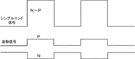
受信側では、コンパレータは受信した論理”1”のシーケンスまたは論理”0”のシーケンスをハイレベルおよびローレベルと比較する。論理”1”のシーケンスが送られたならば、そのシーケンスはハイレベルと比較される。論理”0”のシーケンスが送られたならば、そのシーケンスはローレベルと比較される。 On the receiving side, the comparator compares the received logic "1" sequence or logic "0" sequence with a high level and a low level. If a logic "1" sequence is sent, the sequence is compared to a high level. If a logic "0" sequence is sent, the sequence is compared to a low level.
論理”1”のシーケンスが送られたならば、受信側でその論理”1”のシーケンスはハイレベルと比較される。比較結果が同一であることを示す場合には、コンパレータは論理”0”を出力し、送信リンクにおいて差動信号の転換は起こらず、P−Nがデータの回復のために採用される。比較結果が異なることを示す場合には、コンパレータは論理”1”を出力し、転換制御信号生成モジュール に通知し、反転するようにデータ受信モジュールを制御し、リンクを制御する。すなわち、N−Pがデータの回復のために採用される。 If a logic "1" sequence is sent, the logic "1" sequence is compared to a high level on the receiving side. If the comparison results indicate the same, the comparator outputs a logic "0", no differential signal conversion occurs on the transmission link, and PN is employed for data recovery. If the comparison results indicate different, the comparator outputs a logic “1”, notifies the conversion control signal generation module, controls the data reception module to invert, and controls the link. That is, NP is adopted for data recovery.
送信リンクがマルチチャネル送信を採用する場合には、制御状態マシーンはリンク検出および転換訂正モードに入るように相互接続ノードを制御する。全てのチャネルは、それぞれチャネル検出と転換訂正を実行する。転換が起こらないチャネルは受信側でデータを回復するためにP−Nタイプを採用し、転換が起こるチャネルは受信側でデータを回復するためにNーPタイプを採用する。 If the transmission link employs multi-channel transmission, the control state machine controls the interconnect node to enter link detection and diversion correction mode. All channels perform channel detection and conversion correction, respectively. A channel where no conversion occurs adopts the PN type in order to recover data at the receiving side, and a channel where conversion occurs adopts the NP type in order to recover data at the receiving side.
先行技術に比べて本開示の実施形態は以下の有利な効果を有する。
いくつかの実施形態において、作動信号転換訂正回路および作動信号転換訂正方法は差動信号送信リンクの特徴を十分に考慮し、決定の検出と自動訂正の方法を採用する。これは、高速差動リンクの差動信号の転換の検出と制御を達成し、その一方でマルチチャネルの検出と訂正に並列して適用される。これは、論理設計検証の効率を効果的に改善し、ハードウェアデバッグの複雑さを減少させ、手動で実行される差動制御の困難さと複雑さを補うことができる。作動信号転換訂正回路および作動信号転換訂正方法は、送信リンクの接続性と信号転換の自動的決定を採用し、決定の状況に従って自動的に制御信号を形成し、受信したデータの訂正を制御する。作動信号転換訂正回路および作動信号転換訂正方法は、例えば、FPGAチップの論理設計やASICチップの論理設計への適用のように、広く適用されることができ、確かな実行可能性を持ち、促進することが容易である。
Compared to the prior art, the embodiments of the present disclosure have the following advantageous effects.
In some embodiments, the activation signal conversion correction circuit and the activation signal conversion correction method take into account the characteristics of the differential signal transmission link and employ a method of detection detection and automatic correction. This achieves detection and control of differential signal transitions in high-speed differential links, while being applied in parallel to multi-channel detection and correction. This can effectively improve the efficiency of logic design verification, reduce hardware debug complexity, and compensate for the difficulty and complexity of manually executed differential control. The operation signal conversion correction circuit and the operation signal conversion correction method adopt automatic determination of transmission link connectivity and signal conversion, automatically form a control signal according to the determination situation, and control the correction of received data . The operation signal conversion correction circuit and the operation signal conversion correction method can be widely applied, for example, applied to the logic design of the FPGA chip and the logic design of the ASIC chip, and have a certain feasibility and promotion. Easy to do.
図は、必ずしも縮尺通りに描かれず、一般に例として、しかし制限のためではなく、この出願において議論されるさまざまな実施形態を示す。 The figures are not necessarily drawn to scale and generally illustrate various embodiments discussed in this application by way of example but not limitation.
図面を参照しつつ、ここに開示される作動信号転換訂正回路および作動信号転換訂正方法を以下に詳細に説明する。 The operation signal conversion correction circuit and the operation signal conversion correction method disclosed herein will be described in detail below with reference to the drawings.
図1、2、および3に示すように、ここに開示される作動信号転換訂正回路は2つの相互接続されたノードの間に配置される次のモジュールを含む。
図1における破線の左側に示されるように、データフレーム送信モジュールは第1の入力ポートと第2の入出力ポートと第3の入出力ポートとを有する。入力ポートは、第1のバッファを通ってPラインとNラインに接続される。第2の入出力ポートと第3の入出力ポートは、お互いに並列に接続され、それからそれぞれPラインとNラインに接続される。
As shown in FIGS. 1, 2, and 3, the actuation signal diversion correction circuit disclosed herein includes the following modules disposed between two interconnected nodes.
As shown on the left side of the broken line in FIG. 1, the data frame transmission module has a first input port, a second input / output port, and a third input / output port. The input port is connected to the P line and the N line through the first buffer. The second input / output port and the third input / output port are connected in parallel to each other, and then connected to the P line and the N line, respectively.
図1における破線の右側に示されるように、転換制御信号生成モジュールは、PラインとNラインに接続された第2のバッファ、第2のバッファに直列に接続されたコンパレータ、および制御リンクを有する。制御リンクは、アップリンクすなわち第1の制御スイッチ、およびダウンリンクすなわち第2の制御スイッチを含む。第1の制御スイッチの入力側は構成モジュールに配置され、構成モジュールはバッファとコンパレータの間に位置し、第1の制御スイッチは構成モジュールに直列に接続され、第1の制御スイッチの出力側はそれぞれPラインとNラインに接続される。第2の制御スイッチの入力側はバッファとコンパレータの間に配置され、第2の制御スイッチの出力側はそれぞれPラインとNラインに接続される。 As shown on the right side of the broken line in FIG. 1, the conversion control signal generation module has a second buffer connected to the P line and the N line, a comparator connected in series to the second buffer, and a control link. . The control link includes an uplink or first control switch and a downlink or second control switch. The input side of the first control switch is arranged in the configuration module, the configuration module is located between the buffer and the comparator, the first control switch is connected in series with the configuration module, and the output side of the first control switch is Each is connected to the P line and the N line. The input side of the second control switch is disposed between the buffer and the comparator, and the output side of the second control switch is connected to the P line and the N line, respectively.
ここに開示のいくつかの実施形態は、作動信号転換訂正方法を提供する。その方法の動作プロセスは以下を含む。
リンクがリンクの検出と転換と訂正のモードにあるとき、データフレーム送信モジュールは対応する論理のシーケンスを生成し、送信を終了する。 受信側はシーケンスデータを受信する。コンパレータは受信したシーケンスを比較して処理し、対応するフィードバックまたはチェックを形成し、それによってリンクの検出と差動訂正の目的を達成する。
コンパレータからの比較結果は、転換制御信号生成モジュールに通知される。転換制御信号生成モジュールは、受信したデータの訂正を制御し、リンクが転換操作を実行するか否かを制御する対応する制御シーケンスを生成する。
Some embodiments disclosed herein provide an actuation signal diversion correction method. The operating process of the method includes:
When the link is in link detection, diversion and correction mode, the data frame transmission module generates a corresponding logic sequence and terminates the transmission. The receiving side receives sequence data. The comparator compares and processes the received sequence to form a corresponding feedback or check, thereby achieving the purpose of link detection and differential correction.
The comparison result from the comparator is notified to the conversion control signal generation module. The conversion control signal generation module controls the correction of the received data and generates a corresponding control sequence that controls whether the link performs a conversion operation.
いくつかの実施形態では、その方法の詳細な動作プロセスは以下を含む。
データフレーム送信モジュールは、論理”1”のシーケンスを生成し、第2の入出力ポートと第3の入出力ポートはそのシーケンスを送信する。受信側では、構成モジュールは信号をプルダウンするように制御スイッチを制御し、その一方で第2の入出力ポートと第3の入出力ポートはプルダウンの結果を検出する。検出結果が論理”0”であるならば、そのときそれはリンクが接続されることを示す。そうでなければ、リンクが失敗することを示す。
リンクが接続されたならば、データフレーム送信モジュールは論理”1”または論理”0”のシーケンスを生成し、第1の入力ポートはそのシーケンスの送信を終了する。
In some embodiments, the detailed operational process of the method includes:
The data frame transmission module generates a logic “1” sequence, and the second input / output port and the third input / output port transmit the sequence. On the receiving side, the configuration module controls the control switch to pull down the signal, while the second input / output port and the third input / output port detect the pull-down result. If the detection result is logic “0”, then it indicates that the link is connected. Otherwise, it indicates that the link fails.
If the link is connected, the data frame transmission module generates a logic “1” or logic “0” sequence, and the first input port finishes transmitting the sequence.
受信側では、コンパレータは受信した論理”1”のシーケンスまたは論理”0”のシーケンスをハイレベルおよびローレベルと比較する。論理”1”のシーケンスが送られたならば、そのシーケンスはハイレベルと比較される。論理”0”のシーケンスが送られたならば、そのシーケンスはローレベルと比較される。 On the receiving side, the comparator compares the received logic "1" sequence or logic "0" sequence with a high level and a low level. If a logic "1" sequence is sent, the sequence is compared to a high level. If a logic "0" sequence is sent, the sequence is compared to a low level.
論理”1”のシーケンスが送られたならば、受信側でその論理”1”のシーケンスはハイレベルと比較される。比較結果が同一であることを示す場合には、コンパレータは論理”0”を出力し、送信リンクにおいて差動信号の転換は起こらず、P−Nがデータの回復のために採用される。比較結果が異なることを示す場合には、コンパレータは論理”1”を出力し、転換制御信号生成モジュールに通知し、反転するようにデータ受信モジュールを制御し、リンクを制御する。すなわち、N−Pがデータの回復のために採用される。 If a logic "1" sequence is sent, the logic "1" sequence is compared to a high level on the receiving side. If the comparison results indicate the same, the comparator outputs a logic "0", no differential signal conversion occurs on the transmission link, and PN is employed for data recovery. When the comparison results indicate that the comparison results are different, the comparator outputs a logic “1”, notifies the conversion control signal generation module, controls the data reception module to invert, and controls the link. That is, NP is adopted for data recovery.
送信リンクがマルチチャネル送信を採用する場合には、制御状態マシーンはリンク検出および転換訂正モードに入るように相互接続ノードを制御する。全てのチャネルは、それぞれチャネル検出と転換訂正を実行する。転換が起こらないチャネルは受信側でデータを回復するためにP−Nタイプを採用し、転換が起こるチャネルは受信側でデータを回復するためにNーPタイプを採用する。 If the transmission link employs multi-channel transmission, the control state machine controls the interconnect node to enter link detection and diversion correction mode. All channels perform channel detection and conversion correction, respectively. A channel where no conversion occurs adopts the PN type in order to recover data at the receiving side, and a channel where conversion occurs adopts the NP type in order to recover data at the receiving side.
更に、自動動作を達成するために、状態マシーン制御モジュールは、全体回路で設計されることができ、リンク初期化フェーズにおいて送信リンクをリンク検出と転換訂正モードに入らせるために使われる。これは相互接続されたノードのリンク初期化特性に従って供給される。状態マシーン制御モジュールの具体的な構成は、中国特許出願第CN201010593965.8号、発明の名称「シリアルバスデバイスおよびそのデバイスによるデータ送信方法」で議論された。従って、ここでの開示では同じことをもはや議論しない。 Furthermore, in order to achieve automatic operation, the state machine control module can be designed with a whole circuit and is used to put the transmission link into link detection and diversion correction mode in the link initialization phase. This is provided according to the link initialization characteristics of the interconnected nodes. The specific configuration of the state machine control module was discussed in Chinese Patent Application No. CN20101059395.8, entitled “Serial Bus Device and Data Transmission Method Using the Device”. Thus, the same is no longer discussed in this disclosure.
いくつかの実施形態は決定の検出と自動訂正の方法を採用する。これは、高速差動リンクに対するリンクの差動の転換の検出と制御を達成し、その一方でマルチチャネルの検出と訂正に並列して適用される。これは、論理設計検証の効率を効果的に改善し、ハードウェアデバッグの複雑さを減少させることができる。 Some embodiments employ decision detection and automatic correction methods. This achieves link differential switching detection and control for high speed differential links, while being applied in parallel to multi-channel detection and correction. This can effectively improve the efficiency of logic design verification and reduce hardware debug complexity.
本出願で開示される実施形態は、例であり、非制限的であるとして全ての点で考慮されるべきである。本発明の範囲は、上述の記載よりはむしろ添付された請求項によって示される。そして、請求項と等価の意味と範囲でなされた全ての変化は包含されることが意図される。 The embodiments disclosed in this application are to be considered in all respects as being exemplary and not limiting. The scope of the invention is indicated by the appended claims rather than the foregoing description. All changes made in the equivalent meaning and scope of the claims are intended to be included.
Claims (5)
前記Pラインと前記Nラインに接続された第2のバッファ、当該第2のバッファに直列に接続されたコンパレータ、および制御リンクを有し、当該制御リンクがアップリンクとダウンリンクを含み、当該アップリンクが第1の制御スイッチであり、当該第1の制御スイッチの入力側が構成モジュールに配置され、当該構成モジュールが前記第2のバッファと前記コンパレータの間に位置し、当該第1の制御スイッチが当該構成モジュールに直列に接続され、当該第1の制御スイッチの出力側がそれぞれ前記Pラインと前記Nラインに接続され、前記ダウンロードリンクが第2の制御スイッチであり、当該第2の制御スイッチの入力側が前記バッファと前記コンパレータの間に配置され、当該第2の制御スイッチの出力側がそれぞれ前記Pラインと前記Nラインに接続される転換制御信号生成モジュールと、
を備え、
前記データフレーム送信モジュールと前記転換制御信号生成モジュールが、2つの相互接続されるノードの間に配置される、
ことを特徴とする作動信号転換訂正回路。 A first input port, a second input / output port, and a third input / output port; the first input port is connected to the P line and the N line through the first buffer; The data input / output port and the third input / output port are connected in parallel to each other, and the data frame transmission module is connected to the P line and the N line, respectively.
A second buffer connected to the P line and the N line; a comparator connected in series to the second buffer; and a control link, the control link including an uplink and a downlink, The link is the first control switch, the input side of the first control switch is arranged in the configuration module, the configuration module is located between the second buffer and the comparator, and the first control switch It is connected in series to the component module, the output side of the first control switch is connected to the P line and the N line, respectively, the download link is a second control switch, and the input of the second control switch Is disposed between the buffer and the comparator, and the output side of the second control switch is respectively connected to the P line. A conversion control signal generation module that is connected to the N line and,
With
The data frame transmission module and the conversion control signal generation module are disposed between two interconnected nodes;
An operation signal conversion correction circuit characterized by that.
(2)前記コンパレータからの比較結果が転換制御信号生成モジュールに通知され、当該転換制御信号生成モジュールが受信した前記シーケンスの訂正を制御し、前記リンクが転換操作を実行するか否かを制御する対応する制御シーケンスを生成するステップと、
を備えることを特徴とする作動信号転換訂正方法。 (1) When the link is in the detection, conversion and correction mode of the link, the data frame transmission module generates the corresponding logic sequence and terminates the transmission. The receiving side receives the sequence and the comparator receives it. Comparing and processing the sequences to form corresponding feedback or checks to achieve the purpose of detection of the link and differential correction;
(2) The conversion result from the comparator is notified to the conversion control signal generation module, the correction of the sequence received by the conversion control signal generation module is controlled, and whether or not the link performs a conversion operation is controlled. Generating a corresponding control sequence;
An operation signal conversion correction method comprising:
前記データフレーム送信モジュールが論理”1”のシーケンスを生成し、第2の入出力ポートと第3の入出力ポートが当該シーケンスを送信し、受信側では構成モジュールが信号をプルダウンするように制御スイッチを制御し、その一方で前記第2の入出力ポートと前記第3の入出力ポートがプルダウンの結果を検出し、検出結果が論理”0”であるならば、それは前記リンクが接続されることを示し、そうでなければ、前記リンクが失敗することを示し、
前記リンクが接続されたならば、前記データフレーム送信モジュールが論理”1”または論理”0”のシーケンスを生成し、第1の入力ポートが当該シーケンスの送信を終了する、
ことを特徴とする請求項2に記載の作動信号転換訂正方法。 In the step (1),
Control switch so that the data frame transmission module generates a logic "1" sequence, the second input / output port and the third input / output port transmit the sequence, and the receiving module pulls down the signal On the other hand, if the second input / output port and the third input / output port detect the pull-down result and the detection result is logic “0”, it means that the link is connected. , Otherwise indicate that the link fails,
If the link is connected, the data frame transmission module generates a logic “1” or logic “0” sequence, and the first input port terminates transmission of the sequence.
The operation signal conversion correction method according to claim 2, wherein:
受信側で、前記コンパレータが受信した論理”1”のシーケンスまたは論理”0”のシーケンスをハイレベルおよびローレベルと比較し、論理”1”のシーケンスが送られたならば、当該シーケンスがハイレベルと比較され、論理”0”のシーケンスが送られたならば、当該シーケンスがローレベルと比較され、
論理”1”のシーケンスが送られたならば、受信側で当該論理”1”のシーケンスがハイレベルと比較され、比較結果が同一であることを示す場合には、前記コンパレータが論理”0”を出力し、送信リンクにおいて差動信号の転換は起こらず、P−Nがデータの回復のために採用され、比較結果が異なることを示す場合には、前記コンパレータが論理”1”を出力し、前記転換制御信号生成モジュールに通知し、反転するようにデータ受信モジュールを制御し、リンクを制御し、N−Pがデータの回復のために採用される、
ことを特徴とする請求項3に記載の作動信号転換訂正方法。 In the step (2),
The receiving side compares the logic “1” sequence or logic “0” sequence received by the comparator with the high level and the low level, and if the logic “1” sequence is sent, the sequence is set to the high level. If a logic “0” sequence is sent, the sequence is compared to a low level,
If a logic “1” sequence is sent, the receiving side compares the logic “1” sequence with a high level and indicates that the comparison results are the same. When the transmission link does not cause differential signal conversion and PN is adopted for data recovery and the comparison results indicate different, the comparator outputs a logic “1”. , Notify the conversion control signal generation module, control the data receiving module to invert, control the link, NP is adopted for data recovery,
The operation signal conversion correction method according to claim 3.
送信リンクがマルチチャネル送信を採用する場合には、制御状態マシーンがリンク検出および転換訂正モードに入るように相互接続ノードを制御し、全てのチャネルがそれぞれチャネル検出と転換訂正を実行し、転換が起こらないチャネルが受信側でデータを回復するためにP−Nタイプを採用し、転換が起こるチャネルが受信側でデータを回復するためにNーPタイプを採用する、
ことを特徴とする請求項3に記載の作動信号転換訂正方法。 In the step (2),
If the transmission link employs multi-channel transmission, the control state machine controls the interconnection node to enter link detection and conversion correction mode, all channels perform channel detection and conversion correction respectively, A non-occurring channel adopts a PN type to recover data at the receiving side, and a channel in which a transition occurs adopts an NP type to recover data at the receiving side,
The operation signal conversion correction method according to claim 3.
Applications Claiming Priority (3)
| Application Number | Priority Date | Filing Date | Title |
|---|---|---|---|
| CN201410009245.0A CN103856305B (en) | 2014-01-24 | 2014-01-24 | Differential signal inverse correction circuit and method |
| CN201410009245.0 | 2014-01-24 | ||
| PCT/CN2014/071478 WO2015109564A1 (en) | 2014-01-24 | 2014-01-26 | Differential signal inversion correction circuit and method therefor |
Publications (1)
| Publication Number | Publication Date |
|---|---|
| JP2017508421A true JP2017508421A (en) | 2017-03-23 |
Family
ID=50863553
Family Applications (1)
| Application Number | Title | Priority Date | Filing Date |
|---|---|---|---|
| JP2016565529A Pending JP2017508421A (en) | 2014-01-24 | 2014-01-26 | Operation signal conversion correction circuit and operation signal conversion correction method |
Country Status (4)
| Country | Link |
|---|---|
| EP (1) | EP2938020B1 (en) |
| JP (1) | JP2017508421A (en) |
| CN (1) | CN103856305B (en) |
| WO (1) | WO2015109564A1 (en) |
Families Citing this family (3)
| Publication number | Priority date | Publication date | Assignee | Title |
|---|---|---|---|---|
| CN104717447B (en) * | 2015-03-19 | 2018-07-10 | 武汉精测电子集团股份有限公司 | Realize 16LANE module multichannel MIPI synchronization transfer methods |
| CN104735387B (en) * | 2015-03-19 | 2018-05-22 | 武汉精测电子集团股份有限公司 | Realize multichannel MIPI synchronization transfer methods and device |
| CN109479106B (en) * | 2016-08-22 | 2021-07-20 | 索尼半导体解决方案公司 | Comparator, AD converter, solid-state imaging device, electronic apparatus, and comparator control method |
Citations (7)
| Publication number | Priority date | Publication date | Assignee | Title |
|---|---|---|---|---|
| JPH01288133A (en) * | 1988-05-16 | 1989-11-20 | Mitsubishi Heavy Ind Ltd | Signal transmission equipment |
| JPH0548466A (en) * | 1990-11-30 | 1993-02-26 | Advanced Micro Devices Inc | Differential-signal polarity reverse detector |
| JPH0818605A (en) * | 1994-06-29 | 1996-01-19 | Nippondenso Co Ltd | Automatic polarity correction device for line connection |
| JPH09266496A (en) * | 1996-01-23 | 1997-10-07 | Seiko Epson Corp | Device and method for data reception, and electronic equipment |
| US20040189806A1 (en) * | 2003-03-24 | 2004-09-30 | Berkey Thomas F. | Polarity correction circuit and system incorporating the same |
| WO2008056708A1 (en) * | 2006-11-07 | 2008-05-15 | Sony Corporation | Transmitting device, video signal transmitting method in transmitting device, recieving device and video signal recieving method in recieving device |
| JP2013187584A (en) * | 2012-03-06 | 2013-09-19 | Sony Corp | Data receiving circuit, data transmitting circuit, data transmitting and receiving device, data transmission system, and data receiving method |
Family Cites Families (7)
| Publication number | Priority date | Publication date | Assignee | Title |
|---|---|---|---|---|
| US5903613A (en) * | 1996-01-23 | 1999-05-11 | Seiko Epson Corporation | Data reception device, data reception method and electronic equipment |
| KR100782305B1 (en) * | 2006-01-09 | 2007-12-06 | 삼성전자주식회사 | Data signal transmission Device and Method for Ternary lines differential signaling |
| US8125259B2 (en) * | 2008-01-03 | 2012-02-28 | Agere Systems Inc. | Duty cycle distortion (DCD) jitter modeling, calibration and generation methods |
| CN101567729B (en) * | 2008-04-21 | 2013-07-17 | 北京六合万通微电子技术股份有限公司 | Device for detecting strength of differential signal |
| CN102047623B (en) * | 2008-06-27 | 2013-08-28 | 佳能株式会社 | Differential transmission circuit |
| CN102142987B (en) * | 2010-12-09 | 2014-01-08 | 浪潮(北京)电子信息产业有限公司 | Serial bus equipment and data transmission method thereof |
| JP5917858B2 (en) * | 2011-08-29 | 2016-05-18 | ルネサスエレクトロニクス株式会社 | Semiconductor integrated circuit device |
-
2014
- 2014-01-24 CN CN201410009245.0A patent/CN103856305B/en active Active
- 2014-01-26 EP EP14835547.2A patent/EP2938020B1/en active Active
- 2014-01-26 JP JP2016565529A patent/JP2017508421A/en active Pending
- 2014-01-26 WO PCT/CN2014/071478 patent/WO2015109564A1/en active Application Filing
Patent Citations (9)
| Publication number | Priority date | Publication date | Assignee | Title |
|---|---|---|---|---|
| JPH01288133A (en) * | 1988-05-16 | 1989-11-20 | Mitsubishi Heavy Ind Ltd | Signal transmission equipment |
| US5257287A (en) * | 1990-02-15 | 1993-10-26 | Advanced Micro Devices, Inc. | Automatic polarity detection and correction method and apparatus employing linkpulses |
| JPH0548466A (en) * | 1990-11-30 | 1993-02-26 | Advanced Micro Devices Inc | Differential-signal polarity reverse detector |
| JPH0818605A (en) * | 1994-06-29 | 1996-01-19 | Nippondenso Co Ltd | Automatic polarity correction device for line connection |
| JPH09266496A (en) * | 1996-01-23 | 1997-10-07 | Seiko Epson Corp | Device and method for data reception, and electronic equipment |
| US20040189806A1 (en) * | 2003-03-24 | 2004-09-30 | Berkey Thomas F. | Polarity correction circuit and system incorporating the same |
| JP2004289844A (en) * | 2003-03-24 | 2004-10-14 | Sensormatic Electronics Corp | Polarity correcting circuit and system incorporating the same |
| WO2008056708A1 (en) * | 2006-11-07 | 2008-05-15 | Sony Corporation | Transmitting device, video signal transmitting method in transmitting device, recieving device and video signal recieving method in recieving device |
| JP2013187584A (en) * | 2012-03-06 | 2013-09-19 | Sony Corp | Data receiving circuit, data transmitting circuit, data transmitting and receiving device, data transmission system, and data receiving method |
Also Published As
| Publication number | Publication date |
|---|---|
| EP2938020B1 (en) | 2018-08-22 |
| EP2938020A1 (en) | 2015-10-28 |
| EP2938020A4 (en) | 2016-04-27 |
| CN103856305A (en) | 2014-06-11 |
| CN103856305B (en) | 2017-05-03 |
| WO2015109564A1 (en) | 2015-07-30 |
Similar Documents
| Publication | Publication Date | Title |
|---|---|---|
| US8990460B2 (en) | CPU interconnect device | |
| US20120082463A1 (en) | Electro-optical communications link | |
| US20190044760A1 (en) | Technologies for optimizing transmitter equalization with high-speed retimer | |
| KR20150059728A (en) | Optical memory extension architecture | |
| US9692715B2 (en) | Multiple ethernet ports and port types using a shared data path | |
| CN102195619B (en) | Method and circuit for detecting and eliminating signal glitch | |
| US20130002396A1 (en) | Communication device, communication circuit, and method | |
| JP2017508421A (en) | Operation signal conversion correction circuit and operation signal conversion correction method | |
| WO2017012517A1 (en) | Hybrid physical coding sub-layer and method for transmitting and receiving data, and storage medium | |
| CN104333388A (en) | Serial communication protocol controller, character re-aligning circuit and 8b/10b decoder | |
| CN113193914A (en) | Sending unit, receiving unit, active transmission device and active transmission system suitable for USB signals | |
| EP2933728B1 (en) | Using serdes loopbacks for low latency functional modes with full monitoring capability | |
| JP2011248814A (en) | Device having pci express link error detection and automatic restoration function | |
| US9543949B2 (en) | Differential signal reversion and correction circuit and method thereof | |
| US10417171B1 (en) | Circuits for and methods of enabling the communication of serialized data in a communication link associated with a communication network | |
| US8954623B2 (en) | Universal Serial Bus devices supporting super speed and non-super speed connections for communication with a host device and methods using the same | |
| WO2015024499A1 (en) | Sequence transmission/receiving device and method | |
| CN103441791B (en) | A kind of spaceborne data transmitting device and the system of selection of input signal thereof | |
| KR101528694B1 (en) | Method and device for adjusting line sequences in ethernet transmission | |
| TWI676888B (en) | Systems and methods providing a low-power mode for serial links | |
| CN108121397B (en) | Transmitting circuit and receiving circuit of asynchronous clock domain and digital signal transmitting method thereof | |
| US20240104048A1 (en) | Transmitting Apparatus, Receiving Apparatus, Parameter Adjustment Method, SerDes Circuit, and Electronic Device | |
| US20240070100A1 (en) | Communications device | |
| US20230336198A1 (en) | Smart serdes | |
| JP2022113147A (en) | Area-efficient high-speed sequence generator and error checker |
Legal Events
| Date | Code | Title | Description |
|---|---|---|---|
| A621 | Written request for application examination |
Free format text: JAPANESE INTERMEDIATE CODE: A621 Effective date: 20170112 |
|
| A977 | Report on retrieval |
Free format text: JAPANESE INTERMEDIATE CODE: A971007 Effective date: 20180112 |
|
| A131 | Notification of reasons for refusal |
Free format text: JAPANESE INTERMEDIATE CODE: A131 Effective date: 20180130 |
|
| A02 | Decision of refusal |
Free format text: JAPANESE INTERMEDIATE CODE: A02 Effective date: 20180911 |