JP2017504167A - Board to board connector assembly - Google Patents
Board to board connector assembly Download PDFInfo
- Publication number
- JP2017504167A JP2017504167A JP2016547887A JP2016547887A JP2017504167A JP 2017504167 A JP2017504167 A JP 2017504167A JP 2016547887 A JP2016547887 A JP 2016547887A JP 2016547887 A JP2016547887 A JP 2016547887A JP 2017504167 A JP2017504167 A JP 2017504167A
- Authority
- JP
- Japan
- Prior art keywords
- board
- plug
- header
- receptacle
- connector assembly
- Prior art date
- Legal status (The legal status is an assumption and is not a legal conclusion. Google has not performed a legal analysis and makes no representation as to the accuracy of the status listed.)
- Granted
Links
- 238000003780 insertion Methods 0.000 claims abstract description 44
- 230000037431 insertion Effects 0.000 claims abstract description 44
- 150000003071 polychlorinated biphenyls Chemical class 0.000 claims abstract 2
- 238000005476 soldering Methods 0.000 claims description 16
- 210000000078 claw Anatomy 0.000 claims description 11
- FPWNLURCHDRMHC-UHFFFAOYSA-N 4-chlorobiphenyl Chemical compound C1=CC(Cl)=CC=C1C1=CC=CC=C1 FPWNLURCHDRMHC-UHFFFAOYSA-N 0.000 description 7
- 230000008878 coupling Effects 0.000 description 6
- 238000010168 coupling process Methods 0.000 description 6
- 238000005859 coupling reaction Methods 0.000 description 6
- 238000000034 method Methods 0.000 description 5
- NMWSKOLWZZWHPL-UHFFFAOYSA-N 3-chlorobiphenyl Chemical compound ClC1=CC=CC(C=2C=CC=CC=2)=C1 NMWSKOLWZZWHPL-UHFFFAOYSA-N 0.000 description 4
- 101001082832 Saccharomyces cerevisiae (strain ATCC 204508 / S288c) Pyruvate carboxylase 2 Proteins 0.000 description 4
- 230000009471 action Effects 0.000 description 4
- 230000008569 process Effects 0.000 description 3
- 210000004905 finger nail Anatomy 0.000 description 2
- 238000009434 installation Methods 0.000 description 2
- 230000009467 reduction Effects 0.000 description 2
- 230000000712 assembly Effects 0.000 description 1
- 238000000429 assembly Methods 0.000 description 1
- 238000006073 displacement reaction Methods 0.000 description 1
- 230000000694 effects Effects 0.000 description 1
- 230000013011 mating Effects 0.000 description 1
- 230000007246 mechanism Effects 0.000 description 1
- 238000012986 modification Methods 0.000 description 1
- 230000004048 modification Effects 0.000 description 1
Images


Classifications
-
- H—ELECTRICITY
- H01—ELECTRIC ELEMENTS
- H01R—ELECTRICALLY-CONDUCTIVE CONNECTIONS; STRUCTURAL ASSOCIATIONS OF A PLURALITY OF MUTUALLY-INSULATED ELECTRICAL CONNECTING ELEMENTS; COUPLING DEVICES; CURRENT COLLECTORS
- H01R12/00—Structural associations of a plurality of mutually-insulated electrical connecting elements, specially adapted for printed circuits, e.g. printed circuit boards [PCB], flat or ribbon cables, or like generally planar structures, e.g. terminal strips, terminal blocks; Coupling devices specially adapted for printed circuits, flat or ribbon cables, or like generally planar structures; Terminals specially adapted for contact with, or insertion into, printed circuits, flat or ribbon cables, or like generally planar structures
- H01R12/70—Coupling devices
- H01R12/71—Coupling devices for rigid printing circuits or like structures
- H01R12/72—Coupling devices for rigid printing circuits or like structures coupling with the edge of the rigid printed circuits or like structures
- H01R12/73—Coupling devices for rigid printing circuits or like structures coupling with the edge of the rigid printed circuits or like structures connecting to other rigid printed circuits or like structures
- H01R12/732—Printed circuits being in the same plane
-
- H—ELECTRICITY
- H01—ELECTRIC ELEMENTS
- H01R—ELECTRICALLY-CONDUCTIVE CONNECTIONS; STRUCTURAL ASSOCIATIONS OF A PLURALITY OF MUTUALLY-INSULATED ELECTRICAL CONNECTING ELEMENTS; COUPLING DEVICES; CURRENT COLLECTORS
- H01R13/00—Details of coupling devices of the kinds covered by groups H01R12/70 or H01R24/00 - H01R33/00
- H01R13/02—Contact members
- H01R13/10—Sockets for co-operation with pins or blades
- H01R13/11—Resilient sockets
- H01R13/113—Resilient sockets co-operating with pins or blades having a rectangular transverse section
-
- H—ELECTRICITY
- H01—ELECTRIC ELEMENTS
- H01R—ELECTRICALLY-CONDUCTIVE CONNECTIONS; STRUCTURAL ASSOCIATIONS OF A PLURALITY OF MUTUALLY-INSULATED ELECTRICAL CONNECTING ELEMENTS; COUPLING DEVICES; CURRENT COLLECTORS
- H01R13/00—Details of coupling devices of the kinds covered by groups H01R12/70 or H01R24/00 - H01R33/00
- H01R13/62—Means for facilitating engagement or disengagement of coupling parts or for holding them in engagement
- H01R13/627—Snap or like fastening
- H01R13/6271—Latching means integral with the housing
- H01R13/6273—Latching means integral with the housing comprising two latching arms
-
- H—ELECTRICITY
- H05—ELECTRIC TECHNIQUES NOT OTHERWISE PROVIDED FOR
- H05K—PRINTED CIRCUITS; CASINGS OR CONSTRUCTIONAL DETAILS OF ELECTRIC APPARATUS; MANUFACTURE OF ASSEMBLAGES OF ELECTRICAL COMPONENTS
- H05K1/00—Printed circuits
- H05K1/02—Details
- H05K1/14—Structural association of two or more printed circuits
-
- H—ELECTRICITY
- H01—ELECTRIC ELEMENTS
- H01R—ELECTRICALLY-CONDUCTIVE CONNECTIONS; STRUCTURAL ASSOCIATIONS OF A PLURALITY OF MUTUALLY-INSULATED ELECTRICAL CONNECTING ELEMENTS; COUPLING DEVICES; CURRENT COLLECTORS
- H01R2105/00—Three poles
Landscapes
- Engineering & Computer Science (AREA)
- Microelectronics & Electronic Packaging (AREA)
- Coupling Device And Connection With Printed Circuit (AREA)
Abstract
【解決手段】第1のPCB上に装着されるレセプタクルコネクタと、第2のPCB上に装着されるプラグコネクタとを使用して2つのPCBを接続するように意図される、基板対基板コネクタアセンブリが、前方に開くレセプタクルコネクタのヘッダ上のプラグ挿入空間と、前部上に形成されるプラグコネクタのヘッダのプラグ挿入空間に取り外し可能に挿入される締結具部とともに形成され、各ヘッダは各PCBを垂直に通り抜けるように装着され、製品の垂直幅を減少させる。したがって、締結部をプラグ挿入空間内に係止する係止部が締結部に設けられ、係止部は垂直方向に弾性的に動作するように構成され、第2のPCBを通り抜けるように動作する。【選択図】図1A board-to-board connector assembly intended to connect two PCBs using a receptacle connector mounted on a first PCB and a plug connector mounted on a second PCB. Is formed with a plug insertion space on the header of the receptacle connector that opens forward, and a fastener portion that is removably inserted into the plug insertion space of the header of the plug connector formed on the front portion. It is mounted so that it passes vertically through, reducing the vertical width of the product. Accordingly, a locking portion for locking the fastening portion in the plug insertion space is provided in the fastening portion, and the locking portion is configured to operate elastically in the vertical direction, and operates to pass through the second PCB. . [Selection] Figure 1
Description
本開示は、韓国特許庁に先に出願された、「基板対基板タイプコネクタアセンブリ」と題する、2014年2月20日出願の韓国特許出願第10−2014−0019793号の優先権を主張する。上述の特許出願の内容は、その全体が本明細書に援用される。 The present disclosure claims the priority of Korean Patent Application No. 10-2014-0019793, filed on February 20, 2014, which was previously filed with the Korean Patent Office and entitled “Board to Board Type Connector Assembly”. The contents of the above-mentioned patent applications are incorporated herein in their entirety.
この本開示は、2つのプリント回路基板(PCB)を接続するコネクタアセンブリに一般的に関し、さらに詳細には、LED TVパネル内で2つのPCBを接続する基板対基板コネクタアセンブリに関する。 This disclosure relates generally to connector assemblies that connect two printed circuit boards (PCBs), and more particularly to a board-to-board connector assembly that connects two PCBs in an LED TV panel.
LED TVにおけるように、複数のPCBが配置される場合、PCBを電気的に接続するようにコネクタが設けられる。互いに接続されるPCBは、その上に装着される電子機器の装着表面が単一の平面を形成するように、配置される。ともに接続される2つのPCBのうち、雌コネクタが一方の上に装着され、雄コネクタが他方の上に装着される。 When a plurality of PCBs are arranged as in the LED TV, a connector is provided to electrically connect the PCBs. The PCBs connected to each other are arranged such that the mounting surfaces of the electronic devices mounted thereon form a single plane. Of the two PCBs connected together, the female connector is mounted on one and the male connector is mounted on the other.
同様に、基板(PCB)を基板(PCB)に接続する基板対基板コネクタが、「コネクタ」と題された、韓国特許公開第2012−0127510号において開示される。上述の出願の内容は、その全体が本明細書に援用される。‘510出願によるコネクタは、コネクタを含む回路基板の厚み全体を減少させる目的を有するが、実際、コネクタが基板上に装着される基板上タイプであるため、コネクタを含む基板の厚み全体を減少させる能力は限定される。 Similarly, a board-to-board connector for connecting a board (PCB) to a board (PCB) is disclosed in Korean Patent Publication No. 2012-0127510 entitled “Connector”. The contents of the above-mentioned applications are incorporated herein in their entirety. The connector according to the '510 application has the purpose of reducing the overall thickness of the circuit board including the connector, but in fact it reduces the overall thickness of the board including the connector because the connector is of the on-board type that is mounted on the board. Capabilities are limited.
上述の課題を解決するために考案された本開示の目的は、低プロファイルおよび小型化を実現できる基板対基板コネクタアセンブリを提供することである。 An object of the present disclosure devised to solve the above-described problems is to provide a board-to-board connector assembly that can realize a low profile and a small size.
第1のPCB上に装着されるレセプタクルコネクタおよび第2のPCB上に装着されるプラグコネクタを使用して2つのPCBを接続するように意図される、本開示の基板対基板コネクタアセンブリには、レセプタクルコネクタのヘッダ上で前方に開くプラグ挿入空間と、前部上に形成されるプラグコネクタのヘッダのプラグ挿入空間に取り外し可能に挿入される締結具部が形成され、一方で各ヘッダは、各PCBを垂直に通り抜けるように装着され、その結果、製品の垂直幅を減少させる。したがって、プラグ挿入空間内に締結部を係止する係止部が、締結部内に設けられ、係止部が垂直方向に弾性的に動作するように構成され、第2のPCBを通り抜けるように動作する。 The board-to-board connector assembly of the present disclosure, which is intended to connect two PCBs using a receptacle connector mounted on a first PCB and a plug connector mounted on a second PCB, includes: A plug insertion space that opens forward on the header of the receptacle connector and a fastener portion that is removably inserted into the plug insertion space of the header of the plug connector formed on the front portion are formed, while each header Mounted vertically through the PCB, thereby reducing the vertical width of the product. Accordingly, a locking portion for locking the fastening portion in the plug insertion space is provided in the fastening portion, and the locking portion is configured to operate elastically in the vertical direction, and operates so as to pass through the second PCB. To do.
係止部は、垂直方向に弾性的に動作し、後方に延び、締結部の上面から離間され、締結部の上部の前端を始点とする、押圧レバーおよびレセプタクルヘッダ上に形成される係止溝内に取り外し可能に締結し、押圧レバーから前方に突出する係止突起を備える。押圧レバーが、左右に離間した対として形成され、押圧レバーは押圧部によって後端で互いに接続される。 The locking portion elastically operates in the vertical direction, extends rearward, is spaced from the upper surface of the fastening portion, and is formed on the pressing lever and the receptacle header starting from the front end of the upper portion of the fastening portion. A locking projection is provided that is detachably fastened inside and protrudes forward from the pressing lever. The pressing levers are formed as a pair separated from left and right, and the pressing levers are connected to each other at the rear end by the pressing portion.
プラグ挿入空間の内部上面上に、左右へのずれを防ぐために摺動しながらレバーが挿入されるレバー挿入溝が形成され、その結果、によって締結部がプラグ挿入空間内に確実に締結されることができる。レセプタクルヘッドのプラグ挿入空間の入口およびプラグヘッダの締結部の近傍には、それぞれ突起部および陥凹部が設けられ、その結果、組み立て中に締結部がプラグ挿入空間に挿入されるとき、製品の前後の厚み全体を減少させ、2つのヘッダの確実な結合を保証するために、突起部が陥凹部内に挿入される。 On the inner upper surface of the plug insertion space, there is formed a lever insertion groove into which the lever is inserted while sliding to prevent left-right displacement, and as a result, the fastening portion is securely fastened in the plug insertion space. Can do. Protrusions and recesses are provided near the inlet of the plug insertion space of the receptacle head and the fastening portion of the plug header, respectively. As a result, when the fastening portion is inserted into the plug insertion space during assembly, The protrusion is inserted into the recess to reduce the overall thickness of the and to ensure a secure connection of the two headers.
基板対基板コネクタアセンブリは、下部接触部がレセプタクルヘッダ内に位置し、上部半田付け部が第1のPCBの上面に半田付けされている、折り曲げ構造を有するレセプタクル接触端子と、下部接触部がプラグヘッダ内に位置しており、上部半田付け部が第2のPCBの上面に半田付けされている、折り曲げ構造を有するプラグ接触端子とをさらに備える。基板対基板コネクタアセンブリは、下部がレセプタクルヘッダに固定され、上部半田付け部が第1のPCBの上面に半田付けされる、折り曲げ構造を有するレセプタクル嵌合爪と、下部がプラグヘッダに固定され、上部半田付け部が第2のPCBの上面に半田付けされる、折り曲げ構造を有するプラグ嵌合爪とをさらに備える。 The board-to-board connector assembly includes a receptacle contact terminal having a bent structure in which a lower contact portion is located in the receptacle header and an upper soldering portion is soldered to the upper surface of the first PCB, and a lower contact portion is plugged It further includes a plug contact terminal having a folding structure, which is located in the header and whose upper soldering portion is soldered to the upper surface of the second PCB. The board-to-board connector assembly has a lower part fixed to the receptacle header, an upper soldering part is soldered to the upper surface of the first PCB, and a lower part fixed to the plug header. It further includes a plug fitting claw having a bent structure in which the upper soldering portion is soldered to the upper surface of the second PCB.
各接触端子の半田付け部は各ヘッダの背部に位置し、各嵌合爪の半田付け部は、各ヘッダの隣に位置する。製品の前後の厚みを減少させるために、レセプタクルヘッダの後部およびプラグヘッダの後部には、内部に各接触端子部品の上向き折り曲げ部が挿入される、折り曲げ部挿入溝がそれぞれ形成される。プラグヘッダ上に、折り曲げ部挿入溝が、係止部の後部上にも設けられる。レセプタクル接触端子およびプラグ接触端子は、二重接触構造を有する。 The soldering part of each contact terminal is located on the back part of each header, and the soldering part of each fitting claw is located next to each header. In order to reduce the front and rear thickness of the product, a bent portion insertion groove into which the upward bent portion of each contact terminal component is inserted is formed in the rear portion of the receptacle header and the rear portion of the plug header. On the plug header, a bent portion insertion groove is also provided on the rear portion of the locking portion. The receptacle contact terminal and the plug contact terminal have a double contact structure.
本開示による基板対基板コネクタアセンブリは、次の効果を有する。第一に、レセプタクルコネクタおよびプラグコネクタがPCBを通して装着され、プラグコネクタ上に設けられる押圧レバーの動作空間が、PCBを通り抜けるように形成され、レセプタクル接触端子およびプラグ接触端子が二重接触構造を有するため、低プロファイル構造を実現することができる。第二に、突起部および陥凹部が、レセプタクルコネクタのプラグ挿入空間の入口の近傍およびプラグコネクタの締結部にそれぞれ形成され、これらは、締結部がプラグ挿入空間内に挿入されるとき、突起部および陥凹部が互いに挿入されるように組み立てられるため、組み立てられるとき、2つのコネクタの前後の厚みを減少させ、製品の縮小化を可能にする。第三に、プラグコネクタをレセプタクルコネクタ内に挿入するだけで係止が達成され、プラグコネクタの押圧レバーを押す唯一の行動によって係止が解除され、その結果、2つのコネクタが容易に結合され、結合を外すことができる。第四に、上記の特性のために、2つのPCBがLED TVパネル内に接続されるとき、作業を簡単に行うことができ、省スペース化でき、2つのPCBが容易に結合され、結合を外すことができる。 The board-to-board connector assembly according to the present disclosure has the following effects. First, the receptacle connector and the plug connector are mounted through the PCB, the operation space of the pressing lever provided on the plug connector is formed so as to pass through the PCB, and the receptacle contact terminal and the plug contact terminal have a double contact structure. Therefore, a low profile structure can be realized. Second, a protrusion and a recess are formed in the vicinity of the inlet of the plug insertion space of the receptacle connector and in the fastening portion of the plug connector, respectively, and these are the protrusions when the fastening portion is inserted into the plug insertion space. And because the recesses are assembled so that they are inserted into each other, when assembled, the thickness before and after the two connectors is reduced, allowing a product to be reduced. Third, locking is achieved simply by inserting the plug connector into the receptacle connector, and the locking is released by the sole action of pushing the pressing lever of the plug connector, so that the two connectors are easily coupled, The bond can be removed. Fourth, because of the above characteristics, when two PCBs are connected in the LED TV panel, the work can be done easily, space saving, two PCBs can be easily combined and combined. Can be removed.
本開示の構造および動作の機構および方法が、そのさらなる目的および利点とともに、同じ参照符号が同じ要素を識別する添付図面に関連する、下記の詳細な説明の参照によって最も理解されるであろう。 The structure and operation mechanism and method of the present disclosure, together with further objects and advantages thereof, will be best understood by reference to the following detailed description, taken in conjunction with the accompanying drawings, in which like reference characters identify like elements.
本開示は様々な形の実施形態の影響を受けやすいが、本開示が本開示の原則の例示であるとみなされ、本開示を例証されるものに制限する意図はないという理解とともに、特定の実施形態が、図によって示され、明細書において詳細に説明される。 While this disclosure is susceptible to various forms of embodiments, it is considered that this disclosure is illustrative of the principles of this disclosure and is not intended to limit this disclosure to that illustrated. Embodiments are illustrated by the figures and described in detail in the specification.
このように、特徴または態様への参照は、本開示の一例の特徴または態様を説明するように意図され、そのすべての実施形態が説明される特徴または態様を有さなければならないということを暗示するものではない。さらに、説明が特徴の数を例証することに留意されるべきである。特定の特徴がともに組み合わされて可能性のあるシステム設計を例証する一方、それらの特徴はまた、明示で開示されない他の組み合わせで使用されることもできる。そのため、示される組み合わせは、記載されない限り、制限することを意図されない。 Thus, references to features or aspects are intended to describe exemplary features or aspects of the disclosure, and imply that all embodiments thereof must have the features or aspects described. Not what you want. It should further be noted that the description illustrates the number of features. While particular features may be combined together to illustrate possible system designs, those features can also be used in other combinations not explicitly disclosed. As such, the combinations shown are not intended to be limiting unless otherwise stated.
図に例証される実施形態では、本開示の様々な要素の構造および動きの説明に使用される上、下、左、右、前および後ろなどの方向の表現は絶対的ではなく、相対的である。これらの表現は、要素が図に示される位置にある場合、適切である。しかしながら、要素の位置の説明が変わる場合、これらの表現はそれに従って変更される。 In the embodiments illustrated in the figures, representations of directions such as top, bottom, left, right, front and back used to describe the structure and movement of the various elements of the present disclosure are not absolute, but relative is there. These representations are appropriate when the element is in the position shown in the figure. However, if the description of the position of the elements changes, these representations are changed accordingly.
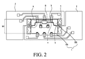
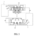
図1〜3は、本開示による基板対基板コネクタアセンブリを例証する。図を参照すると、本開示の基板対基板コネクタアセンブリ1によって接続される第1および第2のPCB2、3は、細長の棒状に形成され、接続部がそれぞれ切り込まれた形状で形成され、一方で切り込まれた部分は互いに相互接続され、接続部を作る。2つのPCB2、3の接続部は、幅がさらに狭い幅方向にそれぞれ形成され、その結果、2つのPCB2、3が、長さがさらに短い幅方向(側方向)に互いに重なり、相互接続される。相互接続部分を有する2つのPCB2、3の左右の幅(幅方向の幅)が、個々のPCB2、3の幅に合致する。このPCB2、3の結合方法で、本開示によるコネクタを適合する製品における、縮小化、即ち、小型化を達成することができる。
1-3 illustrate a board-to-board connector assembly according to the present disclosure. Referring to the figure, the first and
本開示の基板対基板コネクタアセンブリ1が、互いに取り外し可能に結合するレセプタクルコネクタ100およびプラグコネクタ200として構成される、PCB2、3の各接続部に装着される。各コネクタ100、200は、2つのPCB2、3の接続部から横方向を向くように装着される。
The board-to-board connector assembly 1 of the present disclosure is attached to each connection portion of the
さらに、製品の小型化を実現するために、レセプタクルコネクタ100およびプラグコネクタ200が互いに結合される場合、結合部が箱型の形状を有さず、互いに相互接続する形状を有する。言い換えると、図2のAおよびB部分におけるように、レセプタクルコネクタ100の前端部(結合方向に対して)およびプラグコネクタ200が、互いに相互接続して組み立てられる。つまり、レセプタクルコネクタ100の前端部上およびプラグコネクタ200上に、互いに接続される、突起部aおよび陥凹部bが形成され、2つのコネクタ100、200がともに締結される場合、突起部aを陥凹部b内に挿入して組み立てられる。この結合構造によって、2つのコネクタ100、200がともに結合されるときの前後の厚みW1が、レセプタクルコネクタ100の前後の厚みW2とプラグコネクタの前後の厚みW3との合計よりも小さくなり(つまり、W1<W2+W3)、本開示によるコネクタを適応する製品の前後の厚みが減少され得る。突起部aが陥凹部b内に挿入されるように組み立てられるおかげで、2つのコネクタ100、200の結合が、PCBおよび製品が捻られる場合でも、確実に保持されることができ、2つのコネクタ100、200上に設けられる端子間の接触状態が、確実に保持されることができる。
Furthermore, when the
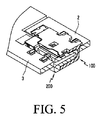
図4〜5を参照すると、本開示の基板対基板コネクタアセンブリ1は、摺動によってともに取り外し可能に結合されるレセプタクルコネクタ100およびプラグコネクタ200を含む。各PCB2、3を通り抜けて設置されるオフセット型としてレセプタクルコネクタ100およびプラグコネクタ200を形成することによって、製品の高さが減少され得る。言い換えると、低プロファイルの製品が達成され得る。
4-5, the board-to-board connector assembly 1 of the present disclosure includes a
レセプタクルコネクタ100は、レセプタクルヘッダ110、レセプタクル嵌合爪120、およびレセプタクル接触端子130を備える。レセプタクルヘッダ110において、下記で説明されるプラグコネクタ200のプラグヘッダ210を構成する締結部211がその中に挿入される、プラグ挿入空間111が、結合方向に対して前方向に開いて形成される。レセプタクルヘッダ110の上部上に、2つの係止穴112が左右に形成され、その中に、下記で説明される押圧レバー241の係止突起242が挿入される。羽根部113がレセプタクルヘッダ110の後部およびいずれかの側部上に形成され、その結果、設置の間にレセプタクルヘッダ110が、後方に滑り落ちないように第1のPCB2の上面上を捉える。
The
レセプタクル嵌合爪120は、レセプタクルヘッダ110を第1のPCB2に固定するように意図され、折り曲げ構造を有し、その下部がレセプタクルヘッダ110のいずれかの側部内に挿入され、一方でその上部の半田付け部がレセプタクルヘッダ110のいずれかの側部上に位置し、第1のPCB2の上面に半田付けされる。レセプタクル接触端子130が、レセプタクルヘッダ110の後部を介したレセプタクルヘッダ110内への挿入によって固定される。このようなレセプタクル接触端子130は、折り曲げ構造を有し、その下部接触部が板状に形成され、レセプタクルヘッダ110のプラグ挿入空間111内に位置し、上部半田付け部がレセプタクルヘッダ110の背部に位置し、第1のPCB2の上部に半田付けされる。
The
プラグコネクタ200は、プラグヘッダ210、プラグ嵌合爪220、プラグ接触端子230、および係止部240を備える。結合方向に対して、締結部211がプラグヘッダ210のいずれかの側部上に形成され、レセプタクルヘッダ110のプラグ挿入空間111内に取り外し可能に挿入されることができ、結合のときに、締結部211の近傍が、相互接続可能な方法でプラグヘッダ210の前部に接触する。プラグヘッダ210の内部に、接触端子挿入穴212が左右に離間して形成され、その中に複数のプラグ接触端子230が下面を介して挿入される。羽根部213がそれぞれレセプタクルヘッダ210の上部のいずれかの側部上に形成され、その結果、設置の間にレセプタクルヘッダ210が、後方に滑り落ちないように第2のPCB3の上面上を捉える。
The
プラグ嵌合爪220は、プラグヘッダ210を第2のPCB3に固定するように意図され、折り曲げ構造を有し、その下部がプラグヘッダ210のいずれかの端部に挿入および固定され、一方でその上部半田付け部がプラグヘッダ210のいずれかの側部上に位置し、第2のPCB3の上部に半田付けされる。プラグ接触端子230が、プラグヘッダ210の下面を介してプラグヘッダ210の接触端子挿入穴212内に挿入および固定される。レセプタクル接触端子230は、折り曲げ構造を有し、その下部接触部が板状に形成され、プラグヘッダ210の接触端子挿入穴212内に位置し、上部半田付け部がプラグヘッダ210の背部に位置し、第2のPCB3の上部に半田付けされる。
The plug
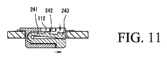
係止部240がプラグヘッダ210の締結部211とともに単体として形成され、プラグヘッダ210の締結部211が、レセプタクルヘッダ110のプラグ挿入空間111に係止され、または係止が外される。係止部240が、上下に弾性的に動作し、後方に延び、締結部211の上面から離間され、締結部211の上面の前端を始点とする一対の押圧レバー241、押圧レバー241の上面から上向きに突出してレセプタクルヘッダ110の係止穴112に嵌合する係止突起242、および係止が解除されるときに押圧されるように設計され、2つの押圧レバー241の後端に接続される押圧部243を備える。押圧部243の上部上に、押圧溝244が形成され、その中に器具または指の爪が挿入され、その結果、器具または指の爪を使用して確実に押下されることができる。締結部211を含むプラグヘッダ210の上部上に、溝状の動作空間214が設けられ、その中で押圧レバー241が動作されることができる。動作空間214が第2のPCB3を通り抜ける位置に設けられるため、押圧レバー241が第2のPCB3を通り抜けるように動作される。このような押圧レバー241の動作構造によって、製品の高さが減少され、低プロファイルを実現する。
The locking
レセプタクルヘッダ110のプラグ挿入空間111内の上面上に、レバー挿入溝114が左右に離間して形成され、その中に、締結部211がプラグ挿入空間内に挿入されるときに、左右への滑りを防ぐように摺動しながら押圧レバー241が挿入される。押圧レバー241がレバー挿入溝114内に摺動される構造のために、締結部211がプラグ挿入空間111内に摺動することで確実に挿入されることができる。したがって、一対の押圧レバー241および係止突起242が締結部211上に設けられ、その結果、2つのコネクタがともに締結するときにクリック感が提供されることができ、2つのコネクタの左右への滑りを防ぐことで端子が接触していることを確実に維持することができる。
A lever insertion groove 114 is formed on the upper surface in the
図7〜11を参照すると、プラグ接触端子230の接触部は、レセプタクル接触端子130の接触部に位置し、接触する、第1の接触部231と、第1の接触部231の上に位置し、第1の接触部231の後端から前方に延びる第2の接触部232とから成り、弾性があり、その結果、レセプタクル接触端子130の接触部が上から押下されるとき、第1の接触端子231に強く接触される。レセプタクル接触端子130は、上面と下面の両方がプラグ接触端子230に接触される二重接触構造を有するおかげで、確実な接触を可能にし、低プロファイルの実現も可能にする。
Referring to FIGS. 7 to 11, the contact portion of the
プラグ挿入空間111内へのプラグヘッダ210の締結部211の挿入の工程で、図8に示されるように、押圧レバー241が押圧されて下降させられ、係止突起242が係止穴112の位置に達するとき、それ自体の弾性によって上昇され、その結果、図9で示されるように、係止穴112内へ自動的に押圧されている係止突起242によって係止が起こる。図11に示されるように、レセプタクルコネクタ100およびプラグコネクタ200を離すために、押圧レバー241の押圧部243が押下され、係止突起242を係止穴112から離し、その結果、2つのコネクタ100、200が容易に係止を外されることができる。上述のように、係止を外すとき、押圧レバー241が第2のPCB3を通り抜けるように動作される。
In the step of inserting the
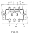
図12を参照すると、レセプタクルヘッダ110の後部上およびプラグヘッダ210上に複数の折り曲げ部挿入溝115、215が形成され、その中に各接触端子130、230の上向きの湾曲部がそれぞれ挿入され、その結果、製品の前後の厚みを減少させることで小型化が達成される。プラグ接触端子230においてプラグヘッダ210の中心に位置する、プラグ接触端子230の湾曲部が、プラグヘッダ210内と係止部240の後部の両方に挿入される、つまり、折り曲げ部挿入溝245も、係止部240を構成する押圧部243の後部上に形成される。接触端子130、230のこの結合構造によって、2つのコネクタ100、200によって占められる空間が圧縮されるため、小型化が達成されることができる。
Referring to FIG. 12, a plurality of bent
本開示の好ましい実施形態が示され、説明されるが、前述の明細書および付属の特許請求の範囲の精神および範囲から逸脱することなく、当業者が様々な変更を考案することが想定される。 While preferred embodiments of the present disclosure have been shown and described, it is envisioned that those skilled in the art will devise various modifications without departing from the spirit and scope of the foregoing specification and the appended claims. .
Claims (14)
第1のプラグ挿入空間であって、前記レセプタクルコネクタのヘッダ上に前方へ開いて配置される、第1のプラグ挿入空間と、
第2のプラグ挿入空間であって、該第2のプラグ挿入空間は、前記プラグコネクタのヘッダ上に配置され、かつ前記プラグコネクタの前部上に形成され、締結具部が前記第2のプラグ挿入空間に取り外し可能に挿入され、係止部が前記締結具部上に設けられ、前記係止部が、前記プラグ挿入空間内で前記締結具部を係止し、かつ前記第2のPCBを通り抜けて垂直方向に弾性的に動作するように構成される、第2のプラグ挿入空間とを備え、
各ヘッダが、前記PCBを垂直に通り抜けるように装着される、基板対基板コネクタアセンブリ。 A board-to-board connector assembly for connecting two PCBs using a receptacle connector mounted on a first printed circuit board (PCB) and a plug connector mounted on a second PCB,
A first plug insertion space, wherein the first plug insertion space is arranged to open forward on the header of the receptacle connector;
A second plug insertion space, the second plug insertion space being disposed on a header of the plug connector and formed on a front portion of the plug connector, wherein a fastener portion is the second plug Removably inserted into the insertion space, a locking part is provided on the fastener part, the locking part locks the fastener part in the plug insertion space, and the second PCB A second plug insertion space configured to elastically move through and vertically through,
A board-to-board connector assembly, wherein each header is mounted to pass vertically through the PCB.
Applications Claiming Priority (3)
| Application Number | Priority Date | Filing Date | Title |
|---|---|---|---|
| KR10-2014-0019793 | 2014-02-20 | ||
| KR1020140019793A KR101626937B1 (en) | 2014-02-20 | 2014-02-20 | Board to board type connector assembly |
| PCT/US2015/016608 WO2015127072A1 (en) | 2014-02-20 | 2015-02-19 | Board-to-board connector assembly |
Publications (2)
| Publication Number | Publication Date |
|---|---|
| JP2017504167A true JP2017504167A (en) | 2017-02-02 |
| JP6258514B2 JP6258514B2 (en) | 2018-01-10 |
Family
ID=53878958
Family Applications (1)
| Application Number | Title | Priority Date | Filing Date |
|---|---|---|---|
| JP2016547887A Expired - Fee Related JP6258514B2 (en) | 2014-02-20 | 2015-02-19 | Board to board connector assembly |
Country Status (5)
| Country | Link |
|---|---|
| US (1) | US9876296B2 (en) |
| JP (1) | JP6258514B2 (en) |
| KR (1) | KR101626937B1 (en) |
| CN (1) | CN106030917B (en) |
| WO (1) | WO2015127072A1 (en) |
Families Citing this family (4)
| Publication number | Priority date | Publication date | Assignee | Title |
|---|---|---|---|---|
| CN106602367B (en) * | 2016-12-14 | 2019-03-26 | 惠州Tcl移动通信有限公司 | A kind of fixed BTB connector is in the fixing piece and mobile terminal of mobile terminal |
| DE112018002369T5 (en) * | 2017-07-18 | 2020-01-23 | Avx Corporation | Contact bridge system from PCB to PCB |
| KR101987593B1 (en) | 2018-03-30 | 2019-06-10 | (주)연호엠에스 | Board to board connector assembly and assembling method of the same |
| TWI694644B (en) * | 2019-04-30 | 2020-05-21 | 禾昌興業股份有限公司 | Buckle connector |
Citations (4)
| Publication number | Priority date | Publication date | Assignee | Title |
|---|---|---|---|---|
| JPH07211408A (en) * | 1994-01-18 | 1995-08-11 | Matsushita Electric Ind Co Ltd | Mounting structure of connector |
| JP2003229190A (en) * | 2002-01-31 | 2003-08-15 | Hon Hai Precision Industry Co Ltd | Electric connector |
| JP2009152039A (en) * | 2007-12-20 | 2009-07-09 | Molex Inc | Terminal and connector |
| JP2012059360A (en) * | 2010-03-31 | 2012-03-22 | Iriso Electronics Co Ltd | Connector |
Family Cites Families (16)
| Publication number | Priority date | Publication date | Assignee | Title |
|---|---|---|---|---|
| US4938701A (en) * | 1988-09-23 | 1990-07-03 | Hayes Microcomputer Products, Inc. | Connecting bracket for modular circuit boards |
| JP2591579Y2 (en) * | 1992-03-19 | 1999-03-03 | バーグ・テクノロジー・インコーポレーテッド | Connector device |
| US5915975A (en) * | 1996-09-12 | 1999-06-29 | Molex Incorporated | Surface mount connector with integrated power leads |
| US6030248A (en) * | 1998-10-29 | 2000-02-29 | Hewlett-Packard Company | Mechanical latch for mating printed circuit board connectors |
| JP3607878B2 (en) | 2001-04-25 | 2005-01-05 | 日本圧着端子製造株式会社 | Flexible board connector |
| US6881075B2 (en) * | 2003-07-08 | 2005-04-19 | Cheng Uei Precision Industry Co., Ltd. | Board-to-board connector |
| KR200359607Y1 (en) | 2004-05-27 | 2004-08-21 | 피-투 인더스트리스 인코포레이티드 | Board to board connector assembly |
| WO2006117892A1 (en) * | 2005-04-28 | 2006-11-09 | Autonetworks Technologies, Ltd. | Electric device |
| US20070141871A1 (en) * | 2005-12-19 | 2007-06-21 | 3M Innovative Properties Company | Boardmount header to cable connector assembly |
| US7618283B1 (en) * | 2008-04-23 | 2009-11-17 | Tyco Electronics Corporation | Bridge connector for connecting circuit boards |
| US7766666B1 (en) * | 2009-08-13 | 2010-08-03 | Cheng Uei Precision Industry Co., Ltd. | Board-to-board connector assembly |
| US7963796B2 (en) * | 2009-10-29 | 2011-06-21 | Tyco Electronics Corporation | Bridge connectors and circuit board assemblies including the same |
| JP2011159587A (en) | 2010-02-03 | 2011-08-18 | Chugoku Electric Power Co Inc:The | Connecting terminal and electronic equipment |
| CN201829646U (en) * | 2010-05-31 | 2011-05-11 | 富士康(昆山)电脑接插件有限公司 | Electric connector component |
| TWI415332B (en) * | 2010-12-31 | 2013-11-11 | Lextar Electronics Corp | Circuit module and electric connector |
| US9515402B1 (en) * | 2015-09-25 | 2016-12-06 | Intel Corporation | Structures for edge-to-edge coupling with flexible circuitry |
-
2014
- 2014-02-20 KR KR1020140019793A patent/KR101626937B1/en active IP Right Grant
-
2015
- 2015-02-19 CN CN201580009689.7A patent/CN106030917B/en not_active Expired - Fee Related
- 2015-02-19 US US15/112,650 patent/US9876296B2/en not_active Expired - Fee Related
- 2015-02-19 JP JP2016547887A patent/JP6258514B2/en not_active Expired - Fee Related
- 2015-02-19 WO PCT/US2015/016608 patent/WO2015127072A1/en active Application Filing
Patent Citations (4)
| Publication number | Priority date | Publication date | Assignee | Title |
|---|---|---|---|---|
| JPH07211408A (en) * | 1994-01-18 | 1995-08-11 | Matsushita Electric Ind Co Ltd | Mounting structure of connector |
| JP2003229190A (en) * | 2002-01-31 | 2003-08-15 | Hon Hai Precision Industry Co Ltd | Electric connector |
| JP2009152039A (en) * | 2007-12-20 | 2009-07-09 | Molex Inc | Terminal and connector |
| JP2012059360A (en) * | 2010-03-31 | 2012-03-22 | Iriso Electronics Co Ltd | Connector |
Also Published As
| Publication number | Publication date |
|---|---|
| CN106030917A (en) | 2016-10-12 |
| KR20150098472A (en) | 2015-08-28 |
| KR101626937B1 (en) | 2016-06-02 |
| CN106030917B (en) | 2019-03-05 |
| WO2015127072A1 (en) | 2015-08-27 |
| US9876296B2 (en) | 2018-01-23 |
| JP6258514B2 (en) | 2018-01-10 |
| US20160352030A1 (en) | 2016-12-01 |
Similar Documents
| Publication | Publication Date | Title |
|---|---|---|
| US9847604B2 (en) | Electrical connector having improved shielding structure | |
| US7666023B2 (en) | Electrical connector with a latch coupled to a pull member | |
| TWI543454B (en) | Shield and locking type board to board connector | |
| JP3474846B2 (en) | Connector latch with integrated auxiliary contacts | |
| US7588443B2 (en) | Board-to-board electrical connector assembly | |
| US20130095676A1 (en) | Electrical connector assembly with compact configuration | |
| CA2676905C (en) | Blade and receptacle power connector | |
| JP5748252B1 (en) | Electronic device and expansion unit for the electronic device | |
| US7857638B2 (en) | Electrical connector with latching members | |
| US20140065849A1 (en) | Connector apparatus | |
| KR20150110333A (en) | Connector | |
| JP2009283233A (en) | Stacking connector | |
| JP6258514B2 (en) | Board to board connector assembly | |
| US7491083B2 (en) | Electrical connector assembly | |
| TWM526206U (en) | Electrical connector | |
| WO2011047539A1 (en) | Electrical connector | |
| US7077678B1 (en) | Electrical connector assembly having board hold down | |
| US20210367379A1 (en) | Strap connector | |
| TWM511148U (en) | Electrical connector and insertion module | |
| JP5329360B2 (en) | Electrical connector | |
| CN108206361B (en) | Connector module | |
| TWM502259U (en) | Plug connector, receptacle connector and electrical connector assembly | |
| JP2019102205A (en) | Electric connector | |
| JP3109261U (en) | Shield and connector with shield | |
| JP2007115538A (en) | Mounting device of electric connector for board |
Legal Events
| Date | Code | Title | Description |
|---|---|---|---|
| A621 | Written request for application examination |
Free format text: JAPANESE INTERMEDIATE CODE: A621 Effective date: 20160721 |
|
| A977 | Report on retrieval |
Free format text: JAPANESE INTERMEDIATE CODE: A971007 Effective date: 20170421 |
|
| A131 | Notification of reasons for refusal |
Free format text: JAPANESE INTERMEDIATE CODE: A131 Effective date: 20170425 |
|
| A521 | Request for written amendment filed |
Free format text: JAPANESE INTERMEDIATE CODE: A523 Effective date: 20170523 |
|
| A131 | Notification of reasons for refusal |
Free format text: JAPANESE INTERMEDIATE CODE: A131 Effective date: 20170912 |
|
| A521 | Request for written amendment filed |
Free format text: JAPANESE INTERMEDIATE CODE: A523 Effective date: 20171129 |
|
| TRDD | Decision of grant or rejection written | ||
| A01 | Written decision to grant a patent or to grant a registration (utility model) |
Free format text: JAPANESE INTERMEDIATE CODE: A01 Effective date: 20171205 |
|
| A61 | First payment of annual fees (during grant procedure) |
Free format text: JAPANESE INTERMEDIATE CODE: A61 Effective date: 20171206 |
|
| R150 | Certificate of patent or registration of utility model |
Ref document number: 6258514 Country of ref document: JP Free format text: JAPANESE INTERMEDIATE CODE: R150 |
|
| LAPS | Cancellation because of no payment of annual fees |