JP2017502173A - Morpholine bath and method for chemically depositing layers - Google Patents
Morpholine bath and method for chemically depositing layers Download PDFInfo
- Publication number
- JP2017502173A JP2017502173A JP2016538718A JP2016538718A JP2017502173A JP 2017502173 A JP2017502173 A JP 2017502173A JP 2016538718 A JP2016538718 A JP 2016538718A JP 2016538718 A JP2016538718 A JP 2016538718A JP 2017502173 A JP2017502173 A JP 2017502173A
- Authority
- JP
- Japan
- Prior art keywords
- bath
- metal
- layer
- sulfur
- morpholine
- Prior art date
- Legal status (The legal status is an assumption and is not a legal conclusion. Google has not performed a legal analysis and makes no representation as to the accuracy of the status listed.)
- Granted
Links
- YNAVUWVOSKDBBP-UHFFFAOYSA-N Morpholine Chemical compound C1COCCN1 YNAVUWVOSKDBBP-UHFFFAOYSA-N 0.000 title claims abstract description 80
- 238000000151 deposition Methods 0.000 title claims abstract description 76
- 238000000034 method Methods 0.000 title claims abstract description 26
- 229910052751 metal Inorganic materials 0.000 claims abstract description 68
- 239000002184 metal Substances 0.000 claims abstract description 68
- 229910052717 sulfur Inorganic materials 0.000 claims abstract description 63
- NINIDFKCEFEMDL-UHFFFAOYSA-N Sulfur Chemical compound [S] NINIDFKCEFEMDL-UHFFFAOYSA-N 0.000 claims abstract description 44
- 239000011593 sulfur Substances 0.000 claims abstract description 43
- 239000000126 substance Substances 0.000 claims abstract description 30
- 150000003839 salts Chemical class 0.000 claims abstract description 24
- 239000002243 precursor Substances 0.000 claims abstract description 17
- -1 morpholine compound Chemical class 0.000 claims abstract description 12
- 230000000737 periodic effect Effects 0.000 claims abstract description 8
- 239000006096 absorbing agent Substances 0.000 claims description 29
- 239000011701 zinc Substances 0.000 claims description 29
- UMGDCJDMYOKAJW-UHFFFAOYSA-N thiourea Chemical compound NC(N)=S UMGDCJDMYOKAJW-UHFFFAOYSA-N 0.000 claims description 22
- 229910052725 zinc Inorganic materials 0.000 claims description 16
- 238000001556 precipitation Methods 0.000 claims description 15
- 150000001875 compounds Chemical class 0.000 claims description 14
- XSQUKJJJFZCRTK-UHFFFAOYSA-N Urea Natural products NC(N)=O XSQUKJJJFZCRTK-UHFFFAOYSA-N 0.000 claims description 11
- 229910052738 indium Inorganic materials 0.000 claims description 10
- HCHKCACWOHOZIP-UHFFFAOYSA-N Zinc Chemical compound [Zn] HCHKCACWOHOZIP-UHFFFAOYSA-N 0.000 claims description 9
- 229910052718 tin Inorganic materials 0.000 claims description 8
- 150000003464 sulfur compounds Chemical class 0.000 claims description 7
- 239000010409 thin film Substances 0.000 claims description 7
- NLXLAEXVIDQMFP-UHFFFAOYSA-N Ammonium chloride Substances [NH4+].[Cl-] NLXLAEXVIDQMFP-UHFFFAOYSA-N 0.000 claims description 6
- VHUUQVKOLVNVRT-UHFFFAOYSA-N Ammonium hydroxide Chemical compound [NH4+].[OH-] VHUUQVKOLVNVRT-UHFFFAOYSA-N 0.000 claims description 6
- 235000011114 ammonium hydroxide Nutrition 0.000 claims description 6
- 229910052711 selenium Inorganic materials 0.000 claims description 6
- 229910052733 gallium Inorganic materials 0.000 claims description 5
- ZOIORXHNWRGPMV-UHFFFAOYSA-N acetic acid;zinc Chemical compound [Zn].CC(O)=O.CC(O)=O ZOIORXHNWRGPMV-UHFFFAOYSA-N 0.000 claims description 4
- 125000003277 amino group Chemical group 0.000 claims description 4
- 229910052976 metal sulfide Inorganic materials 0.000 claims description 4
- XTQHKBHJIVJGKJ-UHFFFAOYSA-N sulfur monoxide Chemical compound S=O XTQHKBHJIVJGKJ-UHFFFAOYSA-N 0.000 claims description 4
- 239000004246 zinc acetate Substances 0.000 claims description 4
- JIAARYAFYJHUJI-UHFFFAOYSA-L zinc dichloride Chemical compound [Cl-].[Cl-].[Zn+2] JIAARYAFYJHUJI-UHFFFAOYSA-L 0.000 claims description 4
- NWONKYPBYAMBJT-UHFFFAOYSA-L zinc sulfate Chemical compound [Zn+2].[O-]S([O-])(=O)=O NWONKYPBYAMBJT-UHFFFAOYSA-L 0.000 claims description 4
- 229960001763 zinc sulfate Drugs 0.000 claims description 4
- 229910000368 zinc sulfate Inorganic materials 0.000 claims description 4
- 239000008139 complexing agent Substances 0.000 claims description 3
- 125000001033 ether group Chemical group 0.000 claims description 3
- 239000011592 zinc chloride Substances 0.000 claims description 2
- 235000005074 zinc chloride Nutrition 0.000 claims description 2
- 230000008021 deposition Effects 0.000 description 56
- 238000000224 chemical solution deposition Methods 0.000 description 25
- QGZKDVFQNNGYKY-UHFFFAOYSA-N Ammonia Chemical compound N QGZKDVFQNNGYKY-UHFFFAOYSA-N 0.000 description 24
- 239000000243 solution Substances 0.000 description 23
- 239000003153 chemical reaction reagent Substances 0.000 description 20
- 229910052984 zinc sulfide Inorganic materials 0.000 description 19
- 229910052760 oxygen Inorganic materials 0.000 description 17
- 239000011541 reaction mixture Substances 0.000 description 16
- 229910021529 ammonia Inorganic materials 0.000 description 12
- 238000006243 chemical reaction Methods 0.000 description 11
- XLOMVQKBTHCTTD-UHFFFAOYSA-N Zinc monoxide Chemical compound [Zn]=O XLOMVQKBTHCTTD-UHFFFAOYSA-N 0.000 description 10
- 238000004519 manufacturing process Methods 0.000 description 8
- 239000000463 material Substances 0.000 description 7
- 239000000654 additive Substances 0.000 description 6
- 229910045601 alloy Inorganic materials 0.000 description 6
- 239000000956 alloy Substances 0.000 description 6
- 239000007864 aqueous solution Substances 0.000 description 6
- 150000002739 metals Chemical group 0.000 description 6
- 230000000996 additive effect Effects 0.000 description 5
- 230000008901 benefit Effects 0.000 description 5
- 229910052793 cadmium Inorganic materials 0.000 description 5
- BDOSMKKIYDKNTQ-UHFFFAOYSA-N cadmium atom Chemical compound [Cd] BDOSMKKIYDKNTQ-UHFFFAOYSA-N 0.000 description 5
- 238000005234 chemical deposition Methods 0.000 description 5
- 230000000694 effects Effects 0.000 description 5
- 239000002244 precipitate Substances 0.000 description 5
- YOXKVLXOLWOQBK-UHFFFAOYSA-N sulfur monoxide zinc Chemical compound [Zn].S=O YOXKVLXOLWOQBK-UHFFFAOYSA-N 0.000 description 5
- 239000011787 zinc oxide Substances 0.000 description 5
- RTZKZFJDLAIYFH-UHFFFAOYSA-N Diethyl ether Chemical compound CCOCC RTZKZFJDLAIYFH-UHFFFAOYSA-N 0.000 description 4
- DVRDHUBQLOKMHZ-UHFFFAOYSA-N chalcopyrite Chemical class [S-2].[S-2].[Fe+2].[Cu+2] DVRDHUBQLOKMHZ-UHFFFAOYSA-N 0.000 description 4
- 230000007062 hydrolysis Effects 0.000 description 4
- 238000006460 hydrolysis reaction Methods 0.000 description 4
- APFVFJFRJDLVQX-UHFFFAOYSA-N indium atom Chemical compound [In] APFVFJFRJDLVQX-UHFFFAOYSA-N 0.000 description 4
- 230000003287 optical effect Effects 0.000 description 4
- 239000000758 substrate Substances 0.000 description 4
- QVGXLLKOCUKJST-UHFFFAOYSA-N atomic oxygen Chemical compound [O] QVGXLLKOCUKJST-UHFFFAOYSA-N 0.000 description 3
- 230000015572 biosynthetic process Effects 0.000 description 3
- 238000010438 heat treatment Methods 0.000 description 3
- 230000006872 improvement Effects 0.000 description 3
- 239000000203 mixture Substances 0.000 description 3
- 231100000252 nontoxic Toxicity 0.000 description 3
- 230000003000 nontoxic effect Effects 0.000 description 3
- 239000006259 organic additive Substances 0.000 description 3
- 239000001301 oxygen Substances 0.000 description 3
- 239000012429 reaction media Substances 0.000 description 3
- MHAJPDPJQMAIIY-UHFFFAOYSA-N Hydrogen peroxide Chemical compound OO MHAJPDPJQMAIIY-UHFFFAOYSA-N 0.000 description 2
- 150000001412 amines Chemical class 0.000 description 2
- 230000005540 biological transmission Effects 0.000 description 2
- 238000005137 deposition process Methods 0.000 description 2
- 239000011521 glass Substances 0.000 description 2
- 230000005855 radiation Effects 0.000 description 2
- 239000004065 semiconductor Substances 0.000 description 2
- 238000003756 stirring Methods 0.000 description 2
- 238000003786 synthesis reaction Methods 0.000 description 2
- YUKQRDCYNOVPGJ-UHFFFAOYSA-N thioacetamide Chemical compound CC(N)=S YUKQRDCYNOVPGJ-UHFFFAOYSA-N 0.000 description 2
- DLFVBJFMPXGRIB-UHFFFAOYSA-N thioacetamide Natural products CC(N)=O DLFVBJFMPXGRIB-UHFFFAOYSA-N 0.000 description 2
- XLYOFNOQVPJJNP-UHFFFAOYSA-N water Substances O XLYOFNOQVPJJNP-UHFFFAOYSA-N 0.000 description 2
- 229910000952 Be alloy Inorganic materials 0.000 description 1
- VEXZGXHMUGYJMC-UHFFFAOYSA-M Chloride anion Chemical compound [Cl-] VEXZGXHMUGYJMC-UHFFFAOYSA-M 0.000 description 1
- 229910000796 S alloy Inorganic materials 0.000 description 1
- QAOWNCQODCNURD-UHFFFAOYSA-L Sulfate Chemical compound [O-]S([O-])(=O)=O QAOWNCQODCNURD-UHFFFAOYSA-L 0.000 description 1
- UCKMPCXJQFINFW-UHFFFAOYSA-N Sulphide Chemical compound [S-2] UCKMPCXJQFINFW-UHFFFAOYSA-N 0.000 description 1
- ATJFFYVFTNAWJD-UHFFFAOYSA-N Tin Chemical compound [Sn] ATJFFYVFTNAWJD-UHFFFAOYSA-N 0.000 description 1
- 239000005083 Zinc sulfide Substances 0.000 description 1
- 229910003363 ZnMgO Inorganic materials 0.000 description 1
- MGTYKZBWBMDCNO-UHFFFAOYSA-N [In].O=S Chemical compound [In].O=S MGTYKZBWBMDCNO-UHFFFAOYSA-N 0.000 description 1
- 239000004480 active ingredient Substances 0.000 description 1
- 230000002411 adverse Effects 0.000 description 1
- 229910052782 aluminium Inorganic materials 0.000 description 1
- XAGFODPZIPBFFR-UHFFFAOYSA-N aluminium Chemical compound [Al] XAGFODPZIPBFFR-UHFFFAOYSA-N 0.000 description 1
- 239000012736 aqueous medium Substances 0.000 description 1
- 150000007514 bases Chemical class 0.000 description 1
- CJOBVZJTOIVNNF-UHFFFAOYSA-N cadmium sulfide Chemical compound [Cd]=S CJOBVZJTOIVNNF-UHFFFAOYSA-N 0.000 description 1
- 229910052951 chalcopyrite Inorganic materials 0.000 description 1
- 238000009388 chemical precipitation Methods 0.000 description 1
- 238000005229 chemical vapour deposition Methods 0.000 description 1
- 230000007547 defect Effects 0.000 description 1
- 238000004925 denaturation Methods 0.000 description 1
- 230000036425 denaturation Effects 0.000 description 1
- 230000001627 detrimental effect Effects 0.000 description 1
- 238000010586 diagram Methods 0.000 description 1
- 229940079593 drug Drugs 0.000 description 1
- 239000003814 drug Substances 0.000 description 1
- 238000004070 electrodeposition Methods 0.000 description 1
- 238000005265 energy consumption Methods 0.000 description 1
- 238000005516 engineering process Methods 0.000 description 1
- 125000000524 functional group Chemical group 0.000 description 1
- 229910001849 group 12 element Inorganic materials 0.000 description 1
- 230000010354 integration Effects 0.000 description 1
- 230000007246 mechanism Effects 0.000 description 1
- 239000002609 medium Substances 0.000 description 1
- 230000008018 melting Effects 0.000 description 1
- 238000002844 melting Methods 0.000 description 1
- 229910021645 metal ion Inorganic materials 0.000 description 1
- 125000000896 monocarboxylic acid group Chemical group 0.000 description 1
- 150000002780 morpholines Chemical class 0.000 description 1
- 231100000956 nontoxicity Toxicity 0.000 description 1
- 238000005457 optimization Methods 0.000 description 1
- 150000002894 organic compounds Chemical class 0.000 description 1
- 239000000575 pesticide Substances 0.000 description 1
- 238000002360 preparation method Methods 0.000 description 1
- 230000002035 prolonged effect Effects 0.000 description 1
- 230000001737 promoting effect Effects 0.000 description 1
- 239000002994 raw material Substances 0.000 description 1
- 238000005546 reactive sputtering Methods 0.000 description 1
- 230000007847 structural defect Effects 0.000 description 1
- 231100000167 toxic agent Toxicity 0.000 description 1
- 239000003440 toxic substance Substances 0.000 description 1
- 231100000419 toxicity Toxicity 0.000 description 1
- 230000001988 toxicity Effects 0.000 description 1
- 230000007704 transition Effects 0.000 description 1
- 239000002699 waste material Substances 0.000 description 1
- DRDVZXDWVBGGMH-UHFFFAOYSA-N zinc;sulfide Chemical compound [S-2].[Zn+2] DRDVZXDWVBGGMH-UHFFFAOYSA-N 0.000 description 1
Images


Classifications
-
- C—CHEMISTRY; METALLURGY
- C23—COATING METALLIC MATERIAL; COATING MATERIAL WITH METALLIC MATERIAL; CHEMICAL SURFACE TREATMENT; DIFFUSION TREATMENT OF METALLIC MATERIAL; COATING BY VACUUM EVAPORATION, BY SPUTTERING, BY ION IMPLANTATION OR BY CHEMICAL VAPOUR DEPOSITION, IN GENERAL; INHIBITING CORROSION OF METALLIC MATERIAL OR INCRUSTATION IN GENERAL
- C23C—COATING METALLIC MATERIAL; COATING MATERIAL WITH METALLIC MATERIAL; SURFACE TREATMENT OF METALLIC MATERIAL BY DIFFUSION INTO THE SURFACE, BY CHEMICAL CONVERSION OR SUBSTITUTION; COATING BY VACUUM EVAPORATION, BY SPUTTERING, BY ION IMPLANTATION OR BY CHEMICAL VAPOUR DEPOSITION, IN GENERAL
- C23C18/00—Chemical coating by decomposition of either liquid compounds or solutions of the coating forming compounds, without leaving reaction products of surface material in the coating; Contact plating
- C23C18/02—Chemical coating by decomposition of either liquid compounds or solutions of the coating forming compounds, without leaving reaction products of surface material in the coating; Contact plating by thermal decomposition
- C23C18/12—Chemical coating by decomposition of either liquid compounds or solutions of the coating forming compounds, without leaving reaction products of surface material in the coating; Contact plating by thermal decomposition characterised by the deposition of inorganic material other than metallic material
- C23C18/1204—Chemical coating by decomposition of either liquid compounds or solutions of the coating forming compounds, without leaving reaction products of surface material in the coating; Contact plating by thermal decomposition characterised by the deposition of inorganic material other than metallic material inorganic material, e.g. non-oxide and non-metallic such as sulfides, nitrides based compounds
-
- C—CHEMISTRY; METALLURGY
- C23—COATING METALLIC MATERIAL; COATING MATERIAL WITH METALLIC MATERIAL; CHEMICAL SURFACE TREATMENT; DIFFUSION TREATMENT OF METALLIC MATERIAL; COATING BY VACUUM EVAPORATION, BY SPUTTERING, BY ION IMPLANTATION OR BY CHEMICAL VAPOUR DEPOSITION, IN GENERAL; INHIBITING CORROSION OF METALLIC MATERIAL OR INCRUSTATION IN GENERAL
- C23C—COATING METALLIC MATERIAL; COATING MATERIAL WITH METALLIC MATERIAL; SURFACE TREATMENT OF METALLIC MATERIAL BY DIFFUSION INTO THE SURFACE, BY CHEMICAL CONVERSION OR SUBSTITUTION; COATING BY VACUUM EVAPORATION, BY SPUTTERING, BY ION IMPLANTATION OR BY CHEMICAL VAPOUR DEPOSITION, IN GENERAL
- C23C2/00—Hot-dipping or immersion processes for applying the coating material in the molten state without affecting the shape; Apparatus therefor
- C23C2/04—Hot-dipping or immersion processes for applying the coating material in the molten state without affecting the shape; Apparatus therefor characterised by the coating material
-
- C—CHEMISTRY; METALLURGY
- C23—COATING METALLIC MATERIAL; COATING MATERIAL WITH METALLIC MATERIAL; CHEMICAL SURFACE TREATMENT; DIFFUSION TREATMENT OF METALLIC MATERIAL; COATING BY VACUUM EVAPORATION, BY SPUTTERING, BY ION IMPLANTATION OR BY CHEMICAL VAPOUR DEPOSITION, IN GENERAL; INHIBITING CORROSION OF METALLIC MATERIAL OR INCRUSTATION IN GENERAL
- C23C—COATING METALLIC MATERIAL; COATING MATERIAL WITH METALLIC MATERIAL; SURFACE TREATMENT OF METALLIC MATERIAL BY DIFFUSION INTO THE SURFACE, BY CHEMICAL CONVERSION OR SUBSTITUTION; COATING BY VACUUM EVAPORATION, BY SPUTTERING, BY ION IMPLANTATION OR BY CHEMICAL VAPOUR DEPOSITION, IN GENERAL
- C23C18/00—Chemical coating by decomposition of either liquid compounds or solutions of the coating forming compounds, without leaving reaction products of surface material in the coating; Contact plating
- C23C18/02—Chemical coating by decomposition of either liquid compounds or solutions of the coating forming compounds, without leaving reaction products of surface material in the coating; Contact plating by thermal decomposition
- C23C18/12—Chemical coating by decomposition of either liquid compounds or solutions of the coating forming compounds, without leaving reaction products of surface material in the coating; Contact plating by thermal decomposition characterised by the deposition of inorganic material other than metallic material
- C23C18/1204—Chemical coating by decomposition of either liquid compounds or solutions of the coating forming compounds, without leaving reaction products of surface material in the coating; Contact plating by thermal decomposition characterised by the deposition of inorganic material other than metallic material inorganic material, e.g. non-oxide and non-metallic such as sulfides, nitrides based compounds
- C23C18/1208—Oxides, e.g. ceramics
- C23C18/1216—Metal oxides
-
- H—ELECTRICITY
- H01—ELECTRIC ELEMENTS
- H01L—SEMICONDUCTOR DEVICES NOT COVERED BY CLASS H10
- H01L31/00—Semiconductor devices sensitive to infrared radiation, light, electromagnetic radiation of shorter wavelength or corpuscular radiation and specially adapted either for the conversion of the energy of such radiation into electrical energy or for the control of electrical energy by such radiation; Processes or apparatus specially adapted for the manufacture or treatment thereof or of parts thereof; Details thereof
- H01L31/0248—Semiconductor devices sensitive to infrared radiation, light, electromagnetic radiation of shorter wavelength or corpuscular radiation and specially adapted either for the conversion of the energy of such radiation into electrical energy or for the control of electrical energy by such radiation; Processes or apparatus specially adapted for the manufacture or treatment thereof or of parts thereof; Details thereof characterised by their semiconductor bodies
- H01L31/0256—Semiconductor devices sensitive to infrared radiation, light, electromagnetic radiation of shorter wavelength or corpuscular radiation and specially adapted either for the conversion of the energy of such radiation into electrical energy or for the control of electrical energy by such radiation; Processes or apparatus specially adapted for the manufacture or treatment thereof or of parts thereof; Details thereof characterised by their semiconductor bodies characterised by the material
- H01L31/0264—Inorganic materials
- H01L31/032—Inorganic materials including, apart from doping materials or other impurities, only compounds not provided for in groups H01L31/0272 - H01L31/0312
- H01L31/0322—Inorganic materials including, apart from doping materials or other impurities, only compounds not provided for in groups H01L31/0272 - H01L31/0312 comprising only AIBIIICVI chalcopyrite compounds, e.g. Cu In Se2, Cu Ga Se2, Cu In Ga Se2
-
- H—ELECTRICITY
- H01—ELECTRIC ELEMENTS
- H01L—SEMICONDUCTOR DEVICES NOT COVERED BY CLASS H10
- H01L31/00—Semiconductor devices sensitive to infrared radiation, light, electromagnetic radiation of shorter wavelength or corpuscular radiation and specially adapted either for the conversion of the energy of such radiation into electrical energy or for the control of electrical energy by such radiation; Processes or apparatus specially adapted for the manufacture or treatment thereof or of parts thereof; Details thereof
- H01L31/0248—Semiconductor devices sensitive to infrared radiation, light, electromagnetic radiation of shorter wavelength or corpuscular radiation and specially adapted either for the conversion of the energy of such radiation into electrical energy or for the control of electrical energy by such radiation; Processes or apparatus specially adapted for the manufacture or treatment thereof or of parts thereof; Details thereof characterised by their semiconductor bodies
- H01L31/0256—Semiconductor devices sensitive to infrared radiation, light, electromagnetic radiation of shorter wavelength or corpuscular radiation and specially adapted either for the conversion of the energy of such radiation into electrical energy or for the control of electrical energy by such radiation; Processes or apparatus specially adapted for the manufacture or treatment thereof or of parts thereof; Details thereof characterised by their semiconductor bodies characterised by the material
- H01L31/0264—Inorganic materials
- H01L31/032—Inorganic materials including, apart from doping materials or other impurities, only compounds not provided for in groups H01L31/0272 - H01L31/0312
- H01L31/0326—Inorganic materials including, apart from doping materials or other impurities, only compounds not provided for in groups H01L31/0272 - H01L31/0312 comprising AIBIICIVDVI kesterite compounds, e.g. Cu2ZnSnSe4, Cu2ZnSnS4
-
- H—ELECTRICITY
- H01—ELECTRIC ELEMENTS
- H01L—SEMICONDUCTOR DEVICES NOT COVERED BY CLASS H10
- H01L31/00—Semiconductor devices sensitive to infrared radiation, light, electromagnetic radiation of shorter wavelength or corpuscular radiation and specially adapted either for the conversion of the energy of such radiation into electrical energy or for the control of electrical energy by such radiation; Processes or apparatus specially adapted for the manufacture or treatment thereof or of parts thereof; Details thereof
- H01L31/18—Processes or apparatus specially adapted for the manufacture or treatment of these devices or of parts thereof
-
- Y—GENERAL TAGGING OF NEW TECHNOLOGICAL DEVELOPMENTS; GENERAL TAGGING OF CROSS-SECTIONAL TECHNOLOGIES SPANNING OVER SEVERAL SECTIONS OF THE IPC; TECHNICAL SUBJECTS COVERED BY FORMER USPC CROSS-REFERENCE ART COLLECTIONS [XRACs] AND DIGESTS
- Y02—TECHNOLOGIES OR APPLICATIONS FOR MITIGATION OR ADAPTATION AGAINST CLIMATE CHANGE
- Y02E—REDUCTION OF GREENHOUSE GAS [GHG] EMISSIONS, RELATED TO ENERGY GENERATION, TRANSMISSION OR DISTRIBUTION
- Y02E10/00—Energy generation through renewable energy sources
- Y02E10/50—Photovoltaic [PV] energy
- Y02E10/541—CuInSe2 material PV cells
Abstract
本発明は、少なくとも金属及び硫黄からなる層を析出させるための化学浴に関する。本発明はまた、このような層を析出させるための方法にも関する。この浴は、溶液中に、周期表のIIB及びIIIA族の少なくとも1種の元素から選択される金属を含む金属塩と、硫黄前駆体とを含む。浴は、モルホリン化合物をさらに含む。The present invention relates to a chemical bath for depositing a layer of at least metal and sulfur. The invention also relates to a method for depositing such a layer. The bath includes, in solution, a metal salt that includes a metal selected from at least one element of groups IIB and IIIA of the periodic table, and a sulfur precursor. The bath further includes a morpholine compound.
Description
本発明は、硫黄及び金属をベースとする層の析出のための化学的析出浴の分野に関する。それは、また、金属及び硫黄をベースとする層を化学的に析出させるための方法にも関する。 The present invention relates to the field of chemical deposition baths for the deposition of sulfur and metal based layers. It also relates to a method for chemically depositing metal and sulfur based layers.
化学浴析出(CBD)法は、例えば薄層(「薄膜」)として合金を製造するために、産業界において一般的に用いられている。これらの方法は、60×30cm2を超える大きな面積を被覆するための、大きなスケールの析出に特に適している。さらに、この技術は、その低コスト及びその技術的単純さに起因して、産業界において広く用いられる。 Chemical bath deposition (CBD) methods are commonly used in industry, for example, to produce alloys as thin layers ("thin films"). These methods are particularly suitable for large scale deposition to cover large areas exceeding 60 × 30 cm 2 . Furthermore, this technology is widely used in industry due to its low cost and its technical simplicity.
このように、化学浴析出は、感光性デバイスの特定の薄層の製造において考慮され得る。より詳細には、いくつかの感光性デバイスにおける吸収体層は、通常、金属及び硫黄を含む合金からなる、いわゆる「バッファ」層によって被覆される。通常、このバッファ層は、硫黄カドミウムCdSの合金からなる。 Thus, chemical bath deposition can be considered in the manufacture of certain thin layers of photosensitive devices. More specifically, the absorber layer in some photosensitive devices is covered by a so-called “buffer” layer, usually made of an alloy containing metal and sulfur. This buffer layer is usually made of an alloy of sulfur cadmium CdS.
カドミウムの毒性は、硫化亜鉛ZnS及びその誘導体などのようなバッファ層に対する代替材料を求めるように我々を促す。しかしながら、如何なる表面上での、特に光吸収体のような他の薄層上での、これらの合金の析出速度は最適ではない。産業界の要求を満たす化学的析出を得るには、15分、又は1時間さえ超える、長いと見なされる時間を伴い得る。このような析出時間の長期化は、製造コストを増やし、デバイスの製造の全連鎖に不利益をもたらす。 The toxicity of cadmium prompts us to seek alternative materials for buffer layers such as zinc sulfide ZnS and its derivatives. However, the deposition rate of these alloys on any surface, especially on other thin layers such as light absorbers, is not optimal. Obtaining chemical deposits that meet industry demands can involve time considered long, exceeding 15 minutes, or even an hour. Such prolonged deposition times increase manufacturing costs and are detrimental to the entire device manufacturing chain.
この理由で、CBDによって、少なくとも硫黄及び金属をベースとする層の析出を達成するための技術的手段を見出すために、特別な注意が払われている。 For this reason, special care is taken to find technical means for achieving deposition of at least sulfur and metal based layers by CBD.
そのような層の析出時間を短縮するために、化学浴における試薬の濃度若しくは温度のいずれかを上げること、又は試薬を予熱することが知られている。しかしながら、これらの3つの手段は、材料及びエネルギーの消費の増大を引き起こすという不都合を有する。それらは、また、析出表面を損傷する恐れもあり得る、又は、追加のコストを招くタイプの、生産の連鎖におけるさらなるステップを伴い得る。 In order to reduce the deposition time of such layers, it is known to either increase the concentration or temperature of the reagent in the chemical bath or to preheat the reagent. However, these three measures have the disadvantage of causing increased material and energy consumption. They may also damage the deposition surface, or may involve additional steps in the production chain of the type that incurs additional costs.
析出速度を加速させるための別の解決策は、化学浴に特別な硫黄前駆体を用いることである。通常、金属及び硫黄の層を析出させるための化学浴は、硫黄前駆体としてチオ尿素溶液を利用する。特許文献1(US2013/0084401)は、チオ尿素をチオアセトアミドによって置き換えることを提案する。しかしながら、この代替案は、チオアセトアミドが強い毒性の化合物であり、それ故、工業用途にあまり適していないという不都合を有する。 Another solution for accelerating the deposition rate is to use special sulfur precursors in the chemical bath. Typically, chemical baths for depositing metal and sulfur layers utilize thiourea solutions as sulfur precursors. Patent document 1 (US2013 / 0084401) proposes replacing thiourea with thioacetamide. However, this alternative has the disadvantage that thioacetamide is a highly toxic compound and is therefore not well suited for industrial applications.
特許文献2(DE102009015063A1)において提案されている別の代替案は、硫黄及び金属をベースとする薄層の析出のために用意される化学浴に、過酸化水素H2O2を添加することにある。この解決策は、H2O2添加剤の腐食性を考えると、析出表面が脆弱であるところ、工業的用途に適していない。 Another alternative proposed in the patent document 2 (DE102009015063A1) is to add hydrogen peroxide H 2 O 2 to a chemical bath prepared for the deposition of a thin layer based on sulfur and metal. is there. This solution is not suitable for industrial use because the precipitation surface is fragile considering the corrosivity of the H 2 O 2 additive.
これらの理由で、本発明者らは、少なくとも硫黄及び金属を含む層の、化学浴における析出速度を増すための、広い範囲の工業的用途に適合する手段を追及する。 For these reasons, we seek a means to suit a wide range of industrial applications to increase the deposition rate in a chemical bath of a layer containing at least sulfur and metal.
上で説明した課題に対処するために、本発明は、少なくとも金属及び硫黄をベースとする層を析出させるための化学浴を提供する。この浴は、溶液中に、
− 周期表のIIB及びIIIA族の少なくとも1種の元素の中から選択される金属を含む金属塩と、
− 硫黄前駆体と
を含む。この浴は、モルホリン化合物をさらに含む。
To address the problems described above, the present invention provides a chemical bath for depositing at least a metal and sulfur based layer. This bath is in solution,
A metal salt comprising a metal selected from at least one element of groups IIB and IIIA of the periodic table;
-A sulfur precursor. The bath further includes a morpholine compound.
このようにして、硫黄と、周期表のIIB又はIIIA族の金属とを含む層の化学的析出のための浴は、浴の溶液混合物にモルホリン型非毒性有機添加剤を添加することによって最適化される。出願人は、モルホリンの添加は、反応促進剤の効果に匹敵する効果を、混合物に作り出すことを見出した。モルホリンは、アンモニアなどのような塩基性pHの溶液のように、その加水分解を促進することにより硫黄前駆体と相互作用するようである。このように、モルホリンの存在は、析出表面での硫黄及び金属ベースの合金の形成を加速することができる。モルホリンは、−NH基(アミン)の存在により提供されるアミン基及びエーテル基(−O−)の両方を有する有機化合物である。これらの二つの基の組み合わせは、それらの統合を錯体に促進する、金属塩のイオン、例えばZn2+上で作用することができる。これらの錯体は、同一層において金属及び硫黄を析出することを可能にする反応に関与される。モルホリンはこのようにして錯化剤として浴において作用する。 In this way, the bath for chemical deposition of a layer containing sulfur and a group IIB or IIIA metal of the periodic table is optimized by adding a morpholine-type non-toxic organic additive to the bath solution mixture. Is done. Applicants have found that the addition of morpholine creates an effect in the mixture that is comparable to that of the reaction promoter. Morpholine appears to interact with the sulfur precursor by promoting its hydrolysis, like a basic pH solution such as ammonia. Thus, the presence of morpholine can accelerate the formation of sulfur and metal based alloys on the precipitation surface. Morpholine is an organic compound having both an amine group and an ether group (—O—) provided by the presence of —NH groups (amine). The combination of these two groups can act on metal salt ions, such as Zn 2+ , which promote their integration into complexes. These complexes are involved in reactions that allow the deposition of metals and sulfur in the same layer. Morpholine thus acts in the bath as a complexing agent.
析出速度の上昇は、金属が、例えば亜鉛Zn又はインジウムInなどのような、IIIA又はIIB族に属する場合に、特に顕著であるように見える。 The increase in the deposition rate appears to be particularly noticeable when the metal belongs to group IIIA or IIB, such as zinc Zn or indium In.
析出速度を上げることに加えて、出願人は、モルホリンの添加により、大きな表面で、金属及び硫黄ベースの均質な層が得られることを見出した。このようにして、化学浴へのモルホリンの添加は、この添加剤を有さない浴を含むCBD析出に比べて、大きな表面積にわたって均質な析出を得ることを可能にしている。 In addition to increasing the deposition rate, Applicants have found that the addition of morpholine results in a metal and sulfur based homogeneous layer on a large surface. In this way, the addition of morpholine to the chemical bath makes it possible to obtain a homogeneous precipitate over a large surface area compared to CBD precipitation including a bath without this additive.
モルホリンの添加によって得られる別の有利な効果は、浴の試薬を予熱することなく析出を行うことができるという事実にある。事前の予熱ステップを省くことによって、工業的規模で、生産速度を上げることが可能である。しかしながら、試薬を予熱することもまた可能であり、これは、上で説明した浴が既存の生産ラインにおいて容易に準備されることを可能にする。 Another advantageous effect obtained by the addition of morpholine lies in the fact that precipitation can take place without preheating the bath reagents. By eliminating the pre-heating step, it is possible to increase the production speed on an industrial scale. However, it is also possible to preheat the reagents, which allows the bath described above to be easily prepared in existing production lines.
化学的析出浴へのモルホリンの添加は、浴の反応混合物に塩基性pHを与えるさらなる利点を有している。8.5の酸性度定数pKaとともに、モルホリンはアンモニア溶液を含まない浴において考慮され得る。CBD析出浴において通常見出されるアンモニアは、化合物の加水分解を促進するために、反応混合物のpHを増大させる機能を有している。この同一の機能は、モルホリンによって有利的に満たされることができ、浴を用意するときに使用される試薬の量を減らす。 The addition of morpholine to the chemical precipitation bath has the further advantage of providing a basic pH to the reaction mixture of the bath. With an acidity constant pKa of 8.5, morpholine can be considered in a bath without ammonia solution. Ammonia usually found in CBD precipitation baths has the function of increasing the pH of the reaction mixture in order to promote the hydrolysis of the compound. This same function can be advantageously fulfilled by morpholine, reducing the amount of reagent used when preparing the bath.
これらの効果は、析出物を生じさせる表面とは無関係である。特に、上で説明した最適化された浴は、例えば、ガラス、金属基板、又は半導体上に、さらには、吸収体のような光起電力性を有する化合物上に、析出物を生じさせることができる。 These effects are independent of the surface that causes the precipitate. In particular, the optimized bath described above can produce precipitates on, for example, glass, metal substrates, or semiconductors, and even on photovoltaic compounds such as absorbers. it can.
これらの効果は、様々な実験構成において観察されており、化学浴における試薬の濃度にかかわらず起こるように見える。しかしながら、反応混合物の化合物のうちの一つの変性閾値以下の温度が有利的に好まれる。 These effects have been observed in various experimental configurations and appear to occur regardless of the reagent concentration in the chemical bath. However, temperatures below the denaturation threshold of one of the compounds of the reaction mixture are advantageously preferred.
有利な一実施形態によれば、モルホリン化合物は浴内で錯化剤として作用するアミン基及びエーテル基を有する。 According to one advantageous embodiment, the morpholine compound has amine and ether groups which act as complexing agents in the bath.
モルホリンのエーテル基及びアミン基は、浴内で使用されるモルホリン化合物における活性基である。これらの基は、上で説明したように、浴の他の試薬の金属イオンを有する錯体を形成することにより、同一層内に金属及び硫黄を析出することに寄与する。 The ether and amine groups of morpholine are active groups in the morpholine compound used in the bath. These groups contribute to depositing metal and sulfur in the same layer by forming complexes with the metal ions of other reagents in the bath, as explained above.
有利な一実施形態によれば、化合物は、化学式C4H9NOを有し得る。 According to one advantageous embodiment, the compound may have the chemical formula C 4 H 9 NO.
この化合物は、有利には、化学浴の他の試薬と混和性である溶液中に存在し得る。化学式C4H9NOのモルホリンの化合物は、特に明らかに見て取れるように、析出速度及び得られる層の均質性を最適化することが認められた。しかしながら、モルホリンの活性成分は、エーテル基及びアミン基を含む誘導分子の延長線(extensive line)においても見出される。他のモルホリンベースの化合物がそれ故予想され得る。 This compound may advantageously be present in a solution that is miscible with the other reagents of the chemical bath. A morpholine compound of formula C 4 H 9 NO was found to optimize the deposition rate and the homogeneity of the resulting layer, as can be seen particularly clearly. However, the active ingredient of morpholine is also found in the extended line of derived molecules containing ether and amine groups. Other morpholine-based compounds can therefore be expected.
一実施形態によれば、0.05mol/Lと1mol/Lの間の濃度の硫黄化合物に対して、0.001mol/Lと10mol/Lの間の濃度のモルホリンが、浴に提供され得る。 According to one embodiment, for a sulfur compound at a concentration between 0.05 mol / L and 1 mol / L, morpholine at a concentration between 0.001 mol / L and 10 mol / L can be provided to the bath.
浴におけるこのような反応混合物は、使用される試薬の量と析出の速さの妥協に対応する。添加剤及び硫黄化合物の量を少なく保つことによって、工業的規模での生産の間にかなりの節減を達成することが可能である。これは、試薬の無駄が少ないことに起因している。 Such a reaction mixture in the bath corresponds to a compromise between the amount of reagent used and the speed of precipitation. By keeping the amount of additives and sulfur compounds small, significant savings can be achieved during production on an industrial scale. This is due to the low waste of reagents.
有利には、金属塩を含む溶液は、0.01mol/Lと1mol/Lの間の濃度の硫酸亜鉛、酢酸亜鉛、及び塩化亜鉛の中から選択される溶液であり得る。 Advantageously, the solution containing the metal salt may be a solution selected from zinc sulfate, zinc acetate, and zinc chloride at a concentration between 0.01 mol / L and 1 mol / L.
金属塩は、周期表のIIB及びIIIA族の他の金属を含み得る。しかしながら、浴における亜鉛金属塩は、析出時間を特に顕著に減少させた。モルホリンなしで、亜鉛金属塩を用いる浴におけるCBD析出に比較して、本発明は、最大で4倍ほど高い析出速度を達成する。 The metal salt may include other metals of groups IIB and IIIA of the periodic table. However, the zinc metal salt in the bath reduced the precipitation time particularly significantly. Compared to CBD deposition in baths with zinc metal salts without morpholine, the present invention achieves a deposition rate as high as 4 times.
金属塩の0.01mol/Lと1mol/Lの間の濃度は、層を析出させるために使用される原材料の量を減らすことを可能にする。 A concentration between 0.01 mol / L and 1 mol / L of the metal salt makes it possible to reduce the amount of raw materials used to deposit the layer.
一実施形態によれば、浴は、10mol/L未満の濃度で、アンモニア溶液をさらに含み得る。 According to one embodiment, the bath may further comprise an ammonia solution at a concentration of less than 10 mol / L.
アンモニア溶液の使用は、硫黄前駆体の加水分解を開始するために化学浴に塩基性pHを与え、それによってそれが金属塩と反応する。 The use of an ammonia solution gives the chemical bath a basic pH to initiate hydrolysis of the sulfur precursor, which reacts with the metal salt.
一実施形態によれば、浴は、いかなるアンモニア溶液を含まなくてよい。 According to one embodiment, the bath may not contain any ammonia solution.
溶液中のモルホリンの自然の塩基特性を考えると、化学浴にアンモニアを添加しないことが可能である。この方法において、本発明は、浴を用意するときに使用される試薬の量を減らすことを可能にしている。アンモニアの酸性度定数より0.75ほど低い8.5の酸性度定数pKaにもかかわらず、モルホリンはアンモニアの効果的な代替であることがわかる。 Given the natural basic properties of morpholine in solution, it is possible not to add ammonia to the chemical bath. In this way, the present invention makes it possible to reduce the amount of reagent used when preparing the bath. Despite the acidity constant pKa of 8.5, which is about 0.75 below the acidity constant of ammonia, it can be seen that morpholine is an effective alternative to ammonia.
一実施形態によれば、硫黄化合物を含む溶液は、チオ尿素CS(NH2)2の溶液であり得る。 According to one embodiment, the solution comprising a sulfur compound can be a solution of thiourea CS (NH 2 ) 2 .
チオ尿素は、硫化物を含む層の析出に特に適した硫黄前駆体である。それは、例えば、感光性デバイス産業において、一般的に用いられている。 Thiourea is a sulfur precursor that is particularly suitable for depositing sulfide-containing layers. It is commonly used, for example, in the photosensitive device industry.
チオ尿素は、モルホリン及び金属塩の存在下における特に速い析出を可能にする。このようにして、チオ尿素が使用された場合に得られる析出速度は、20nmの厚さの、金属硫化物又はオキシ硫化物の層に対して、5分未満であり得る。 Thiourea allows for particularly fast precipitation in the presence of morpholine and metal salts. Thus, the deposition rate obtained when thiourea is used can be less than 5 minutes for a metal sulfide or oxysulfide layer with a thickness of 20 nm.
より詳細には、前記金属は、IIB族の元素であり得る。 More particularly, the metal may be a group IIB element.
IIB族の金属は、感光性デバイス産業にとって特に興味深いものである。これらのデバイスにおいて、カドミウム又は亜鉛などのような金属が、感光性セルの吸収体と前面電気コンタクトとの間のバッファ層に存在し得る。それ故、IIB族の元素は、バッファ層の作成を意図した化学浴に特に適している。 Group IIB metals are of particular interest to the photosensitive device industry. In these devices, a metal such as cadmium or zinc may be present in the buffer layer between the absorber of the photosensitive cell and the front electrical contact. Therefore, group IIB elements are particularly suitable for chemical baths intended to make buffer layers.
特定の一実施形態において、前記金属は亜鉛であり得る。 In one particular embodiment, the metal can be zinc.
CBDによる硫化又はオキシ硫化亜鉛の層の析出は、その光学的性質及び無毒性に起因して、例えば感光性デバイス産業において興味深い。そのような合金からなる層は、CdSのバッファ層に対する効果的で無毒性の代替であり、同時に、500nm未満の波長の放射をより多く透過させる。 The deposition of sulfurized or zinc oxysulfide layers by CBD is of interest for example in the photosensitive device industry due to its optical properties and non-toxicity. Layers made of such alloys are an effective and non-toxic alternative to CdS buffer layers, while at the same time more transmitting radiation at wavelengths below 500 nm.
硫化又はオキシ硫化亜鉛の層は、CdS層より大きなエネルギーバンドギャップを有し、それ故、500nm未満の波長の光を、CdS層より多く透過させる。加えて、硫化又はオキシ硫化亜鉛の層は、感光性デバイスの前面電気コンタクトを形成するためにしばしば使用される酸化亜鉛ZnOの層の光透過特性と同等の光透過特性を有する。 The layer of sulfided or zinc oxysulfide has a larger energy band gap than the CdS layer and therefore transmits more light with a wavelength of less than 500 nm than the CdS layer. In addition, the sulfided or zinc oxysulfide layer has a light transmission property comparable to that of the zinc oxide ZnO layer often used to form the front electrical contact of the photosensitive device.
本発明は、また、溶液中に、
− 周期表のIIB及びIIIA族の少なくとも1種の元素の中から選択される金属を含む金属塩と、
− 硫黄前駆体と
を含む浴において、少なくとも金属及び硫黄をベースとする層を、化学的に析出させるための方法にも関する。
The present invention also provides:
A metal salt comprising a metal selected from at least one element of groups IIB and IIIA of the periodic table;
It also relates to a method for chemically depositing at least a metal and sulfur based layer in a bath comprising a sulfur precursor.
さらに、前記浴には、モルホリン化合物が含まれる。 Further, the bath contains a morpholine compound.
化学浴へのモルホリンの添加を用いる、少なくとも金属及び硫黄をベースとする層の、CBD析出は、上で説明したいくつかの利点をもたらす。浴へのモルホリンの添加は、析出速度を増大させ、より均質な層の実現を可能にし、化学浴の試薬を予熱する先のステップを省略する可能性に起因して、準備時間を節減することができる。 CBD deposition of at least metal and sulfur based layers with the addition of morpholine to the chemical bath provides several advantages as described above. Addition of morpholine to the bath increases the deposition rate, enables a more homogeneous layer, and saves preparation time due to the possibility of omitting the previous step of preheating the chemical bath reagents. Can do.
特定の一実施形態において、層は、金属硫化物をベースとし得る。 In one particular embodiment, the layer may be based on a metal sulfide.
金属硫化物、例えばZnSは、感光性デバイスにおける用途に特に適した合金であり得る。例えば、それは、感光性デバイスの吸収体上のバッファ層として使用され得る。 Metal sulfides, such as ZnS, can be alloys that are particularly suitable for use in photosensitive devices. For example, it can be used as a buffer layer on an absorber of a photosensitive device.
別の実施形態において、層は、金属オキシ硫化物をベースとし得る。 In another embodiment, the layer can be based on a metal oxysulfide.
金属オキシ硫化物、例えば、Zn(S,O)、Zn(S,O,OH)、又はInx(S,O)y、Inx(S,O,OH)y(ここで、0<x<2、及び、0<y<3)は、感光性デバイス産業の要求に特に適した光学的性質を有することができる。それらは、また、感光層上のバッファ層としての使用にも適切であり得る。 Metal oxysulfides such as Zn (S, O), Zn (S, O, OH), or In x (S, O) y , In x (S, O, OH) y (where 0 <x <2 and 0 <y <3) can have optical properties that are particularly suited to the requirements of the photosensitive device industry. They may also be suitable for use as a buffer layer on the photosensitive layer.
有利には、析出の間の浴の温度は、40℃と100℃の間であり得る。 Advantageously, the temperature of the bath during precipitation can be between 40 ° C and 100 ° C.
100℃未満の、特に70℃未満の析出温度は、析出時間の増加によって不利益をもたらされることなく、低い融点を有する合金を含むデバイスへの損傷がより少ない作業環境を可能にする。加えて、反応媒体の温度を下げることにより、CBD析出浴のより少ない加熱に起因して、エネルギーを節減することが可能である。これらの節減は、浴の大きさと共に増加し、工業的規模では数平方メートルに達し得る。 A deposition temperature of less than 100 ° C., particularly less than 70 ° C., allows a working environment with less damage to devices including alloys with low melting points without being penalized by increased deposition times. In addition, by reducing the temperature of the reaction medium, it is possible to save energy due to less heating of the CBD precipitation bath. These savings increase with bath size and can reach several square meters on an industrial scale.
一実施形態によれば、金属及び硫黄をベースとする層は、光起電力特性を有する層の上に析出されてもよく、光起電力特性を有する前記層は、薄膜ソーラーセルの吸収体を形成する。 According to one embodiment, a metal and sulfur based layer may be deposited on a layer having photovoltaic properties, said layer having photovoltaic properties comprising an absorber of a thin film solar cell. Form.
この様に、金属及び硫黄をベースとする層は、薄膜光起電力セルの吸収体上に析出されて、吸収体を前面電気コンタクトに連結する、バッファ層を示すことができる。感光性セルの吸収体とバッファ層との間の境界の品質は、得られるデバイスにおいて高い変換効率を達成するのに極めて重要である。上で説明した化学的析出法を吸収体上のバッファ層の析出へ応用することは、10分未満で、吸収体自体への損傷なしに析出され、モルホリンを含まない浴で析出されたバッファ層の半分の多さの欠陥を有する、均質な層を生じる。 Thus, a metal and sulfur based layer can be deposited on the absorber of a thin film photovoltaic cell to represent a buffer layer that connects the absorber to the front electrical contact. The quality of the boundary between the absorber of the photosensitive cell and the buffer layer is crucial to achieving high conversion efficiency in the resulting device. Applying the chemical deposition method described above to the deposition of a buffer layer on the absorber takes less than 10 minutes and is deposited without damaging the absorber itself and deposited in a morpholine-free bath. Result in a homogeneous layer with half as many defects.
方法を実施することによって得られるバッファ層の品質に起因して、得られる光起電力デバイスは、14%を超える変換効率を有することができる。 Due to the quality of the buffer layer obtained by carrying out the method, the resulting photovoltaic device can have a conversion efficiency of more than 14%.
光起電力セル吸収体上のバッファ層の析出のための化学浴への添加剤としてモルホリンを用いることは、直観でわかるものではないことが注目されるべきである。実際、モルホリンはゴム産業において、または薬及び農薬の合成のために一般的に使用される。 It should be noted that the use of morpholine as an additive to the chemical bath for the deposition of the buffer layer on the photovoltaic cell absorber is not intuitive. In fact, morpholine is commonly used in the rubber industry or for the synthesis of drugs and pesticides.
吸収体は、Cu(In,Ga)(S,Se)2、Cu2(Zn,Sn)(S,Se)4、及びそれらの誘導体の中のカルコパイライト型化合物をベースとし得る。 Absorber, Cu (In, Ga) ( S, Se) 2, Cu 2 (Zn, Sn) (S, Se) 4, and may based chalcopyrite compounds in those derivatives.
これらの化合物には、例えば、Cu(In,Ga)Se2、CuInSe2、CuInS2、CuGaSe2、Cu2(Zn,Sn)S4、及びCu2(Zn,Sn)Se4が含まれ得る。これらの吸収体が亜鉛及びスズを含む場合、これらの化合物は、CZTSと呼ばれることがある。 These compounds may include, for example, Cu (In, Ga) Se 2 , CuInSe 2 , CuInS 2 , CuGaSe 2 , Cu 2 (Zn, Sn) S 4 , and Cu 2 (Zn, Sn) Se 4. . When these absorbers contain zinc and tin, these compounds are sometimes referred to as CZTS.
上で挙げられたソーラーセル吸収体は、20%を超え得る変換効率を有する、CIGS及びCZTS薄膜セル及びそれらの誘導体の吸収体に相当する。これらの吸収体上にバッファ層を析出させるための上で説明した方法の利用は、これがもたらす性能の向上を考えれば、特に有利である。例えば、カルコパイライト型化合物をベースとする吸収体上に、ZnS、Zn(S,O)、又はZn(S,O,OH)のバッファ層を、このようにして析出させることによって、14%を超える変換効率、並びに、他の析出方法によって得られるデバイスで観察されるものより大きい、最終デバイスの開路(open circuit)電圧及び短絡電流を得ることが可能である。 The solar cell absorbers listed above correspond to absorbers of CIGS and CZTS thin film cells and their derivatives with a conversion efficiency that can exceed 20%. The use of the method described above for depositing the buffer layer on these absorbers is particularly advantageous in view of the performance improvements that this provides. For example, by depositing a buffer layer of ZnS, Zn (S, O) or Zn (S, O, OH) on an absorber based on a chalcopyrite type compound in this way, 14% It is possible to obtain an open circuit voltage and short circuit current of the final device that is greater than that observed with devices obtained by other deposition methods, as well as higher conversion efficiencies.
本発明の方法は、例示の目的で記載されるが、決して限定ではない、いくつかの例示的実施形態の以下の説明を読むことによって、また添付図を見ることにより、よりよく理解されるであろう。 The method of the present invention will be better understood by reading the following description of several exemplary embodiments, which are described for purposes of illustration but are in no way limiting, and by looking at the accompanying figures. I will.
明確にするために、これらの図面に示される様々な要素の寸法は、それらの実際の寸法には必ずしも比例していない。図面において、同じ参照符号は、同じ要素に対応している。 For clarity, the dimensions of the various elements shown in these drawings are not necessarily proportional to their actual dimensions. In the drawings, the same reference numerals correspond to the same elements.
本発明は、改善された化学的析出浴、及び改善されたCBD析出方法に関連している。この改善は、特に、析出速度を顕著に上げることを目指す。例えば向上した析出の品質などのような他の有利な効果も本発明との関連において得られた。 The present invention relates to an improved chemical deposition bath and an improved CBD deposition method. This improvement aims especially at significantly increasing the deposition rate. Other advantageous effects such as improved deposition quality have also been obtained in the context of the present invention.
例として下で与えられる実施形態において、光起電力セル吸収体上のバッファ層の、CBDによる析出という特定の場合が説明される。しかしながら、本発明はまた、下でさらに再述されるように、他の任意のタイプの表面での析出にも適用できる。 In the embodiment given below by way of example, the specific case of CBD deposition of a buffer layer on a photovoltaic cell absorber is described. However, the present invention is also applicable to deposition on any other type of surface, as further described below.
少なくとも硫黄及び金属を含む薄層を析出することに関連して、図1は、基板101、裏面金属コンタクト102、及び吸収体層103を備える、初期試料100の例を示す。したがって、示されている初期試料100は、薄膜感光性デバイスの未完成部分を示す。例として、放射を電流に変換することを意図する吸収体103は、Cu(In,Ga)(S,Se)2、Cu2(Zn,Sn)(S,Se)4、及びそれらの誘導体の中の化合物の1つのような、カルコパイライト型化合物であり得る。これらの誘導体は、より一般的にはCIGS及びCZTSと呼ばれる、例えば、Cu(In,Ga)Se2、CuInSe2、CuInS2、CuGaSe2、Cu2(Zn,Sn)S4、又は、Cu2(Zn,Sn)Se4を含み得る。
In connection with depositing a thin layer containing at least sulfur and metal, FIG. 1 shows an example of an
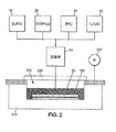
この感光性デバイスの製造を完成するために、本発明は、図2に概略的に示された、化学浴のためのチャンバ200を提案する。CBD析出のためのほとんどの化学浴と同じく、チャンバ200は、カバー220によって閉じることができる。このチャンバ200は、選ばれた濃度の試薬の混合物からなる溶液50を含む。試料100は、この溶液50中にある。この反応媒体を加熱するための手段が備えられ得る。図2において、そのような手段は、反応媒体を含むチャンバを取り囲む水浴210によって示されている。モータ230もまた、溶液50を撹拌する撹拌機構を駆動するために使用され得る。
In order to complete the manufacture of this photosensitive device, the present invention proposes a
図2は、また、反応混合物50をなす溶液を得るためのステップの要約も示す。
FIG. 2 also shows a summary of the steps for obtaining a solution that forms the
図2に示された例において、化学浴は、光起電力デバイスのバッファ層の析出のために構成されている。この理由で、それは、硫酸亜鉛ZnSO4であるとして示された、金属塩を含む第1の水溶液10から調製される。硫黄前駆体を含む第2の水溶液20もまた準備される。この第2の溶液は、化学式CS(NH2)2のチオ尿素であるとして示されている。反応混合物に塩基性pHをもたせるための、アンモニア30もまた任意に準備され得る。アンモニアの存在に起因した塩基性となる媒体は、前駆体と金属塩の反応を促進する。最後に、モルホリン系有機添加剤を含む第4の水溶液40が準備される。この第4の溶液40は、化学式C4H9NOのモルホリンを含むとして示されている。
In the example shown in FIG. 2, the chemical bath is configured for the deposition of the buffer layer of the photovoltaic device. For this reason, it is prepared from a first
下で記載されるように、最初の3つの溶液に対する代替が想定できる。 As described below, an alternative to the first three solutions can be envisaged.
次いで、これらの4つの溶液10、20、30、40は、反応混合物50を生成するために混合される。反応混合物50は、試料100が浸漬されている溶液である。
These four
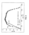
有利には、モルホリンの添加は、吸収体上にZnSの析出を達成するのに要する時間を、かなり短縮する。節約される時間を例示するために、図3のグラフは、3つの異なる条件下に測定された、CBDによる薄層の析出速度を比較している。 Advantageously, the addition of morpholine significantly shortens the time required to achieve ZnS precipitation on the absorber. To illustrate the time saved, the graph of FIG. 3 compares the deposition rate of a thin layer by CBD, measured under three different conditions.
析出したZnS層は、酸素を含み、Zn(S,O)又はZn(S,O,OH)型の層を形成し得る。以下では、「ZnS層」が、純粋なZnSの層、及びZn(S,O)又はZn(S,O,OH)の層を参照するために用いられる。 The deposited ZnS layer contains oxygen and can form a Zn (S, O) or Zn (S, O, OH) type layer. In the following, “ZnS layer” is used to refer to a pure ZnS layer and a Zn (S, O) or Zn (S, O, OH) layer.
曲線301は、反応混合物50が従来の構成である場合に、様々な厚さのZnS層を析出させるのに要する時間を示す。「従来の」は、0.65mol/Lのチオ尿素濃度、0.15mol/LのZnSO4濃度、及び2mol/Lのアンモニア濃度を意味すると理解される。前記試薬は、全て、80℃の温度に予熱され、その後、80℃の同じ温度にしたチャンバに入れられた。
曲線302は、反応混合物50が、特に有利な実施形態に対応する、実験室で試験された構成を備える場合に、様々な厚さのZnS層を析出させるのに要する時間を示す。それは、0.4mol/Lのチオ尿素濃度、0.1mol/LのZnSO4濃度、及び2mol/Lのアンモニア濃度によって特徴づけられる。試薬の予熱は行われず、析出温度は70℃である。
曲線303は、反応混合物50が、曲線302に関連するものと同じ特徴を備えるが、2.2mol/Lの濃度のモルホリンを添加した場合に、様々な厚さのZnS層を析出させるのに要する時間を示す。以下の表1は、上で説明した3つの構成を要約している。

図3の3つの曲線301、302、及び303の推移から、化学浴へのC4H9NOの添加が、ZnS層の析出速度を顕著に増加させることが明らかである。特に、20nmの厚さの層を得るために、本発明により最適化された浴は、析出時間を、従来技術に比べて2.5分の1に、有機添加剤なしで同じ条件下に実施された析出に比べて、5分の1未満にする。
From the transition of the three
加えて、本出願人の化学浴における析出条件は、材料節減及びエネルギー節減において、より効率的であることが注目されるべきである。これは、より低い試薬濃度、より低い析出温度、及び試薬の予熱がないことの結果である。 In addition, it should be noted that the deposition conditions in Applicants' chemical baths are more efficient in material and energy savings. This is a result of lower reagent concentrations, lower deposition temperatures, and no reagent preheating.
上で説明した実施例は、有利には、図4に示される完成した光起電力デバイスを結果として生成できる。 The embodiment described above can advantageously result in the completed photovoltaic device shown in FIG.
図4は、図1のものと同じ構造要素を備える薄膜ソーラーセルを概略的に示す。示されたデバイス400は、上で説明したように、CBDによって吸収体上に析出されたバッファ層104を、さらに備える。バッファ層104上にわたって、例えば真性酸化亜鉛又はZnMgOの、第1ウインドウ層105が、反応性スパッタリング、化学気相堆積、電着、CBD析出、又はILGAR(登録商標)析出などの周知の技術によって堆積され得る。次いで、前面電気コンタクト106が堆積され得る。例えば、それは、アルミニウムがドーピングされた酸化亜鉛ZnOの層であり得る。
FIG. 4 schematically shows a thin film solar cell comprising the same structural elements as in FIG. The illustrated
バッファ層を析出させるための、上で説明した化学浴の使用に固有の他の利点は、得られる光起電力デバイスの性能に現れる。 Another advantage inherent in the use of the chemical bath described above for depositing the buffer layer appears in the performance of the resulting photovoltaic device.
表2は、カルコパイライト型CIGS吸収体を備える、図4のソーラーセルのようなソーラーセルの技術的特徴を比較している。第1のセルは、図3の曲線301に関連して上で説明した、従来の析出条件下で得られたZnSバッファ層を備える。第2のセルは、図3の曲線303に関連して説明したものと同じ条件下で、本発明の浴を含むCBD析出プロセスによって得られたZnSバッファ層を備える。第3のセルは、従来の析出条件下でCBDによって得られたCdSバッファ層を備える。
Table 2 compares the technical characteristics of a solar cell, such as the solar cell of FIG. 4, with a chalcopyrite CIGS absorber. The first cell comprises a ZnS buffer layer obtained under conventional deposition conditions as described above in connection with
表2の各セルは、5×5cm2の表面積、及び20nmの厚さのバッファ層を有する。 Each cell in Table 2 has a surface area of 5 × 5 cm 2 and a buffer layer of 20 nm thickness.
表2の列は、3つのソーラーセルの各々に対する4つのパラメータを示す。第1列は、ソーラーセルの変換効率を示す。第2列は、各セルの形状因子を示し、バッファ層と吸収体との間の境界の品質の目安を与える。第3列は、開路電圧Vocを示す。この電圧が高いほど、セルの電気的性質は良好である。第4列は、短絡電流Jscを示す。この電流が大きいほど、セルの電気的性質は良好である。 The column in Table 2 shows the four parameters for each of the three solar cells. The first column shows the conversion efficiency of the solar cell. The second column shows the form factor of each cell and gives an indication of the quality of the boundary between the buffer layer and the absorber. The third column shows the open circuit voltage Voc. The higher this voltage, the better the electrical properties of the cell. The fourth column shows the short circuit current Jsc. The greater this current, the better the electrical properties of the cell.
表2の各セル、及び各パラメータに対して、対応する値の標準偏差が示されている。この情報は、セルの均質性の評価を与える。セルの内でパラメータがより大きく変動するほど、関連する標準偏差はより大きい。このような不安定性は、セルにおける構造欠陥を示しており、比較される3つのセルの間で実質的な相違を示す唯一の層であるバッファ層において、なおさらそうである。 For each cell and each parameter in Table 2, the standard deviation of the corresponding value is shown. This information gives an assessment of cell homogeneity. The more the parameter varies within the cell, the greater the associated standard deviation. Such instabilities are indicative of structural defects in the cell, and more so in the buffer layer, the only layer that shows substantial differences between the three cells being compared.
表2の値から、本発明に関連して開発されたCBD析出方法によって形成されたZnSバッファ層を有するセルが、他のセルより優れた均質性を有することが明らかである。特に、それは、従来のCBD析出によって形成されたZnS層を有するセルより高い均質性を有する。 From the values in Table 2, it is clear that cells having a ZnS buffer layer formed by the CBD deposition method developed in connection with the present invention have better homogeneity than other cells. In particular, it has a higher homogeneity than a cell with a ZnS layer formed by conventional CBD deposition.
さらに、本発明の方法によって製造されたセルは、他のセルの変換効率より大きな変換効率、さらには改善した電気的性質を有する。 Furthermore, the cell produced by the method of the present invention has a conversion efficiency greater than that of other cells, and even improved electrical properties.
本発明の方法によって得られたセルの形状因子は、CdSバッファ層を有するセルの形状因子と同等である。それにもかかわらず、モルホリンの添加によるCBD析出によって作られたセルの全体の均質性は、より良好である。したがって、モルホリンの添加を用いる析出方法は、大きな表面積の感光性セルの作成に、又は、より一般的には、工業的背景において金属及び硫黄を含む層の作成に、よく適し得る。 The form factor of the cell obtained by the method of the present invention is equivalent to the form factor of the cell having the CdS buffer layer. Nevertheless, the overall homogeneity of the cells made by CBD precipitation with the addition of morpholine is better. Thus, deposition methods using the addition of morpholine may be well suited for making large surface area photosensitive cells, or more generally for making metal and sulfur containing layers in an industrial context.
電子顕微鏡による観察は、本発明の方法を実施することによって得られた析出の構造的品質に関するこれらの観察を裏付けた。 Electron microscope observations confirmed these observations regarding the structural quality of the precipitates obtained by carrying out the method of the present invention.
開発された化学浴、及びバッファ層を生成するためにそれを用いる方法は、適合した析出条件下で、例えばカドミウムを含まない、無毒性材料のバッファ層を得ることを可能にする。 The developed chemical bath and the method of using it to produce a buffer layer make it possible to obtain a buffer layer of non-toxic material, for example free of cadmium, under suitable deposition conditions.
硫化及びオキシ硫化亜鉛のバッファ層の改善した電気的及び光学的性質は、CdSバッファ層のものと比較して、層の量子効率を計算することによって分析された。 The improved electrical and optical properties of the sulfided and zinc oxysulfide buffer layers were analyzed by calculating the quantum efficiency of the layer compared to that of the CdS buffer layer.
図5は、曲線502によって示されるZnSバッファ層での300nmと1000nmの間の量子効率を、曲線501によって示されるCdSバッファ層でのものと比較するグラフである。量子効率は、感光性デバイスによって作成された電子の量と、受け取られた光子の量との間の比を示すパラメータである。
FIG. 5 is a graph comparing the quantum efficiency between 300 nm and 1000 nm in the ZnS buffer layer indicated by
図5において、ZnSバッファ層は、500nm未満の波長でのより良好な光の変換が可能であることが明らかである。電流におけるこの向上は、CdSに比べて、これらの波長でのZnSにおけるより大きな光透過率によって説明できる。この光学的性質は、それ自体、CdSより大きなエネルギーバンドギャップを有する材料のバンド構造の結果である。 In FIG. 5, it is clear that the ZnS buffer layer is capable of better light conversion at wavelengths below 500 nm. This improvement in current can be explained by the greater light transmission in ZnS at these wavelengths compared to CdS. This optical property is itself a result of the band structure of the material having an energy band gap greater than CdS.
本発明は、例として上で説明した実施形態に限定されず、他の変形形態にも及ぶ。実際に、上で説明した浴、並びに金属及び硫黄を含む薄層を作成するためにこの浴を用いる方法は、上で説明した析出速度及び得られた層の品質の増加からの利益を全て得る様々な構成で実施できる。 The invention is not limited to the embodiment described above by way of example, but extends to other variants. Indeed, the bath described above, and the method of using this bath to make a thin layer containing metal and sulfur, all benefit from the deposition rate described above and the increase in quality of the resulting layer. It can be implemented in various configurations.
それ故に、反応混合物50の様々な成分の濃度は調節可能である。経済性のために、試薬の濃度を低下させることが好ましい。しかしながら、低下した濃度は、所定の厚さの薄層を作成するのに要する時間を増大させる傾向がある。上で説明した実施例は、濃度と反応速度の妥協に対応する。異なる要求に応じるために、他の濃度及び他の温度を用いることが可能である。例えば、所定の厚さの薄層を、一定時間の制約内で、析出させるために、濃度及び温度を調節することは、興味深いことであり得る。実際に、通常は増加する析出速度に起因して、妥当な時間内に、例えば1時間未満で、150nmを超える厚さの層を達成するために、添加剤としてモルホリンを用いるCBD析出を使用することが可能である。
Therefore, the concentration of the various components of the
析出速度を増すことによって、低温での反応混合物を得ることが可能である。約70℃の温度を通常は伴う従来の析出技術に比べて、本発明は、温度が60℃未満である、例えば40℃まで下げた場合でさえ、15分未満で析出物を得ることを可能にする。 By increasing the deposition rate, it is possible to obtain a reaction mixture at low temperatures. Compared to conventional deposition techniques that normally involve a temperature of about 70 ° C., the present invention is able to obtain precipitates in less than 15 minutes even when the temperature is below 60 ° C., for example down to 40 ° C. To.
析出速度と試薬の濃度の妥協は、0.01mol/Lと1mol/Lの間の金属塩濃度、0.05mol/Lと1mol/Lの間の硫黄前駆体濃度、0.001mol/Lと10mol/Lの間のモルホリン濃度、及び0.1mol/Lと10mol/Lの間のアンモニア濃度に対して、満足のいくものであると考えられる。 The compromise between deposition rate and reagent concentration is: metal salt concentration between 0.01 mol / L and 1 mol / L, sulfur precursor concentration between 0.05 mol / L and 1 mol / L, 0.001 mol / L and 10 mol. A morpholine concentration between / L and an ammonia concentration between 0.1 mol / L and 10 mol / L is considered satisfactory.
しかしながら、浴及びそれを用いる方法は、アンモニアの添加なしで、想定され得る。例えば、塩基性pHの別の化合物、又は7を超えるpKaの化合物に置き換えること、またはそれを浴から取り除くことが可能である。この試薬を取り除くことにより、析出の速度または質に悪影響を及ぼすことなく、CBD析出工程の費用はまして実施するよりも低い。 However, the bath and the method of using it can be envisaged without the addition of ammonia. For example, it is possible to replace with another compound at basic pH, or a compound with a pKa greater than 7, or remove it from the bath. By removing this reagent, the cost of the CBD deposition process is even lower than that performed without adversely affecting the rate or quality of the deposition.
最小でも、化学浴の反応混合物は、モルホリン、硫黄前駆体及び金属塩だけを含み得る。これらの塩基性化合物をこえて、反応混合物の合成物は上で詳しく述べたものと異なり得る。 At a minimum, the chemical bath reaction mixture may contain only morpholine, sulfur precursors and metal salts. Beyond these basic compounds, the synthesis of the reaction mixture may differ from that detailed above.
特に、より短い、またはより長い官能基を含む他のモルホリン系化合物を用いることが可能である。有利的に、この化合物は硫黄前駆体の加水分解を確かにするために溶液に塩基性pHを与える。 In particular, it is possible to use other morpholine compounds containing shorter or longer functional groups. Advantageously, this compound provides a basic pH to the solution to ensure hydrolysis of the sulfur precursor.
チオ尿素もまた、好ましくは同等の化学的性質を有する、他の硫黄前駆体によって置き換えられてもよい。 Thiourea may also be replaced by other sulfur precursors, preferably with comparable chemistry.
硫酸亜鉛以外で、金属塩は、上で説明したものと同じ応用で、塩化又は酢酸亜鉛によって置き換えられてもよい。例えば式Zn[CH3COOH]2の酢酸亜鉛は、無水であっても、又は、水和していてもよい。インジウム系又はカドミウム系の塩もまた、感光性デバイスにバッファ層を作成する場合の金属塩として適切であり得る。 Other than zinc sulfate, the metal salt may be replaced by chloride or zinc acetate in the same application as described above. For example, zinc acetate of formula Zn [CH 3 COOH] 2 may be anhydrous or hydrated. Indium-based or cadmium-based salts may also be suitable as metal salts when creating buffer layers in photosensitive devices.
さらに、硫黄及び亜鉛の層の析出が水性媒体中で行われる場合、酸素が析出層に組み入れられて、Zn(S,O)又はZn(S,O,OH)型のオキシ硫化亜鉛を形成し得る。同様に、インジウムのような別の金属元素を含む層に酸素を組み入れて、Inx(S,O)y又はInx(S,O,OH)y型のオキシ硫化インジウムを形成することが可能である。しかしながら、周期表のIIB及びIIIA族の他の元素もまた、亜鉛、インジウム、又はカドミウムの化学的性質に似たそれらの化学的性質に起因して、前記金属として考えられ得る。 Further, when the deposition of the sulfur and zinc layers is carried out in an aqueous medium, oxygen is incorporated into the deposited layer to form Zn (S, O) or Zn (S, O, OH) type zinc oxysulfide. obtain. Similarly, oxygen can be incorporated into a layer containing another metal element such as indium to form In x (S, O) y or In x (S, O, OH) y type indium oxysulfide. It is. However, other elements of groups IIB and IIIA of the periodic table can also be considered as said metals due to their chemistry similar to that of zinc, indium, or cadmium.
上で述べられたように、感光性セル吸収体上のバッファ層の析出以外の状況で、上で説明した方法を適用することが可能である。実際に、本発明は、また、ガラス、半導体基板、及び金属のような他の析出表面でも、成功裏に試験された。 As mentioned above, the method described above can be applied in situations other than the deposition of the buffer layer on the photosensitive cell absorber. In fact, the present invention has also been successfully tested on other deposited surfaces such as glass, semiconductor substrates, and metals.
より一般的には、上で説明した本発明は、硫黄及び金属を含む薄層の析出のための化学浴を最適化する。この最適化は、析出速度を増加し、同時に、得られる層の構造的品質を改善し、また材料及びエネルギーを節減する。加えて、本発明は、CBD化学的析出のための既存の化学浴に適合しているという利点を有し、大きな表面積への工業的規模のCBD析出に有利な溶液を提供する。 More generally, the invention described above optimizes the chemical bath for the deposition of thin layers containing sulfur and metals. This optimization increases the deposition rate and at the same time improves the structural quality of the resulting layer and saves material and energy. In addition, the present invention has the advantage of being compatible with existing chemical baths for CBD chemical deposition and provides a solution that is advantageous for industrial scale CBD deposition on large surface areas.
100 (初期)試料
101 基板
102 裏面金属接点
103 吸収体層
104 バッファ層
105 第1窓層
106 前面電気接点
10 金属塩を含む第1の水溶液
20 硫黄前駆体を含む第2の水溶液
30 アンモニア
40 過硫酸塩系無機添加剤を含む第4の水溶液
50 溶液(反応混合物)
200 チャンバ
210 水浴
220 カバー
230 モータ
400 デバイス
100 (Initial)
Claims (16)
− 周期表のIIB及びIIIA族の少なくとも1種の元素の中から選択される金属を含む金属塩(10)と、
− 硫黄前駆体(20)と
を含み、
モルホリン化合物(40)をさらに含むことを特徴とする浴。 A chemical bath for depositing at least a metal and sulfur based layer (104) in a solution (50);
A metal salt (10) comprising a metal selected from at least one element of groups IIB and IIIA of the periodic table;
A sulfur precursor (20),
A bath characterized by further comprising a morpholine compound (40).
− 周期表のIIB及びIIIA族の少なくとも1種の元素の中から選択される金属を含む金属塩(10)と、
− 硫黄前駆体(20)と
を含む浴において、少なくとも金属及び硫黄をベースとする層(104)を化学的に析出させるための方法であって、
モルホリン化合物(40)が前記浴にさらに提供されることを特徴とする前記方法。 In solution (50),
A metal salt (10) comprising a metal selected from at least one element of groups IIB and IIIA of the periodic table;
A method for chemically depositing at least a metal and sulfur based layer (104) in a bath comprising a sulfur precursor (20), comprising:
The method as described above, wherein a morpholine compound (40) is further provided to the bath.
Applications Claiming Priority (2)
| Application Number | Priority Date | Filing Date | Title |
|---|---|---|---|
| FR1362539A FR3014909B1 (en) | 2013-12-12 | 2013-12-12 | MORPHOLINE BATH AND METHOD FOR CHEMICAL DEPOSITION OF A LAYER. |
| PCT/FR2015/050350 WO2015087022A1 (en) | 2013-12-12 | 2015-02-12 | Morpholine bath and method for chemically depositing a layer |
Publications (2)
| Publication Number | Publication Date |
|---|---|
| JP2017502173A true JP2017502173A (en) | 2017-01-19 |
| JP6169283B2 JP6169283B2 (en) | 2017-07-26 |
Family
ID=50289929
Family Applications (1)
| Application Number | Title | Priority Date | Filing Date |
|---|---|---|---|
| JP2016538718A Active JP6169283B2 (en) | 2013-12-12 | 2015-02-12 | Morpholine bath and method for chemically depositing layers |
Country Status (6)
| Country | Link |
|---|---|
| US (1) | US20160312347A1 (en) |
| EP (1) | EP3080334B1 (en) |
| JP (1) | JP6169283B2 (en) |
| FR (1) | FR3014909B1 (en) |
| TW (1) | TW201527592A (en) |
| WO (1) | WO2015087022A1 (en) |
Families Citing this family (1)
| Publication number | Priority date | Publication date | Assignee | Title |
|---|---|---|---|---|
| TWI583017B (en) * | 2015-11-27 | 2017-05-11 | 賴志煌 | Method of manufacturing thin film solar cells |
Citations (3)
| Publication number | Priority date | Publication date | Assignee | Title |
|---|---|---|---|---|
| JP2008510310A (en) * | 2004-08-18 | 2008-04-03 | ハーン−マイトネル−インスチツート ベルリン ゲゼルシャフト ミット ベシュレンクテル ハフツング | Method of applying a zinc sulfide buffer layer by chemical bath deposition on an absorption layer of a semiconductor substrate, in particular a chalcopyrite thin film solar cell |
| US20130084401A1 (en) * | 2010-01-28 | 2013-04-04 | Manz Cigs Technology Gmbh | Bath Deposition Solution for the Wet-Chemical Deposition of a Metal Sulfide Layer and Related Production Method |
| JP2013512306A (en) * | 2009-11-25 | 2013-04-11 | イー・アイ・デュポン・ドウ・ヌムール・アンド・カンパニー | CZTS / Se precursor ink, CZTS / Se thin film, and method for producing CZTS / Se photovoltaic cell |
Family Cites Families (3)
| Publication number | Priority date | Publication date | Assignee | Title |
|---|---|---|---|---|
| US3630763A (en) * | 1969-03-21 | 1971-12-28 | Chapman Chem Co | Control of transit stain on wood products |
| US6454846B2 (en) * | 2000-02-23 | 2002-09-24 | Seiko Epson Corporation | Ink composition suitable for use in ink jet recording |
| US7306663B2 (en) * | 2003-08-05 | 2007-12-11 | Halox, Division Of Hammond Group, Inc. | Corrosion inhibitor |
-
2013
- 2013-12-12 FR FR1362539A patent/FR3014909B1/en active Active
-
2014
- 2014-12-12 TW TW103143576A patent/TW201527592A/en unknown
-
2015
- 2015-02-12 JP JP2016538718A patent/JP6169283B2/en active Active
- 2015-02-12 EP EP15706911.3A patent/EP3080334B1/en active Active
- 2015-02-12 WO PCT/FR2015/050350 patent/WO2015087022A1/en active Application Filing
- 2015-02-12 US US15/103,694 patent/US20160312347A1/en not_active Abandoned
Patent Citations (3)
| Publication number | Priority date | Publication date | Assignee | Title |
|---|---|---|---|---|
| JP2008510310A (en) * | 2004-08-18 | 2008-04-03 | ハーン−マイトネル−インスチツート ベルリン ゲゼルシャフト ミット ベシュレンクテル ハフツング | Method of applying a zinc sulfide buffer layer by chemical bath deposition on an absorption layer of a semiconductor substrate, in particular a chalcopyrite thin film solar cell |
| JP2013512306A (en) * | 2009-11-25 | 2013-04-11 | イー・アイ・デュポン・ドウ・ヌムール・アンド・カンパニー | CZTS / Se precursor ink, CZTS / Se thin film, and method for producing CZTS / Se photovoltaic cell |
| US20130084401A1 (en) * | 2010-01-28 | 2013-04-04 | Manz Cigs Technology Gmbh | Bath Deposition Solution for the Wet-Chemical Deposition of a Metal Sulfide Layer and Related Production Method |
Also Published As
| Publication number | Publication date |
|---|---|
| EP3080334B1 (en) | 2021-09-22 |
| TW201527592A (en) | 2015-07-16 |
| WO2015087022A1 (en) | 2015-06-18 |
| US20160312347A1 (en) | 2016-10-27 |
| FR3014909A1 (en) | 2015-06-19 |
| FR3014909B1 (en) | 2016-01-29 |
| WO2015087022A8 (en) | 2015-11-12 |
| EP3080334A1 (en) | 2016-10-19 |
| JP6169283B2 (en) | 2017-07-26 |
Similar Documents
| Publication | Publication Date | Title |
|---|---|---|
| US20140220728A1 (en) | Methods of forming semiconductor films including i2-ii-iv-vi4 and i2-(ii,iv)-iv-vi4 semiconductor films and electronic devices including the semiconductor films | |
| Shi et al. | Kesterite-based next generation high performance thin film solar cell: current progress and future prospects | |
| JP5564688B2 (en) | CBD solution for CZTS semiconductor, method for producing buffer layer for CZTS semiconductor, and photoelectric device | |
| Seo et al. | Effect of sulfur and copper amounts in sol–gel precursor solution on the growth, crystal properties, and optical properties of Cu 2 ZnSnS 4 films | |
| JP4549570B2 (en) | Method for manufacturing heterojunction thin film solar cell | |
| Echendu et al. | Electrochemical deposition and characterization of ZnOS thin films for photovoltaic and photocatalysis applications | |
| JP2015526884A (en) | Precursor solution for forming semiconductor thin films based on CIS, CIGS, or CZTS | |
| Ullah et al. | Electrodeposition of CuGaSe 2 and CuGaS 2 thin films for photovoltaic applications | |
| Saha | A status review on Cu2ZnSn (S, Se) 4-based thin-film solar cells | |
| Mkawi | Kesterite Cu2ZnSnS4 thin films synthesized utilizing electrodeposition: Influence of metal doping on the properties | |
| Guo et al. | Sol-gel synthesis of Cu2ZnSnS4 thin films under mild conditions | |
| Shafi et al. | Optimization of electrodeposition time on the properties of Cu2ZnSnS4 thin films for thin film solar cell applications | |
| JP6169283B2 (en) | Morpholine bath and method for chemically depositing layers | |
| Banu et al. | Analysis of sulphur deficiency defect prevalent in SILAR-CdS films | |
| Mkawi et al. | Solution-processed sphere-like Cu2ZnSnS4 nanoparticles for solar cells: effect of oleylamine concentration on properties | |
| KR101484156B1 (en) | Process of preparing tin-doped indium sulfide thin film | |
| Bagade et al. | Synthesis of (CdZn) Se thin films by a facile aqueous phase route and their photoelectrochemical performance for solar cell application | |
| JP6035122B2 (en) | Photoelectric conversion element and method for producing buffer layer of photoelectric conversion element | |
| JP6184602B2 (en) | Persulfate bath and method for chemically depositing layers | |
| Seo et al. | Control of metal salt ratio and MoS 2 layer thickness in a Cu 2 ZnSnS 4 thin film solar cell | |
| Kauk-Kuusik et al. | Cu 2 ZnSnS 4 monograin layer solar cells for flexible photovoltaic applications | |
| Gallanti et al. | Ammonia‐free, room temperature, and reusable photochemical bath for the deposition of Zn (S, O) buffer layers in Cu (In, Ga) Se2 thin‐film solar cells | |
| Joshi et al. | Morphological engineering of novel nanocrystalline Cu2Sn (S, Se) 3 thin film through annealing temperature variation: assessment of photoelectrochemical cell performance | |
| JP6121791B2 (en) | Aqueous composition, metal sulfide thin film, metal sulfide particles, and photoelectric conversion element | |
| KR102284809B1 (en) | Cis based thin film, solar cell comprising the thin film and fabrication method thereof |
Legal Events
| Date | Code | Title | Description |
|---|---|---|---|
| A977 | Report on retrieval |
Free format text: JAPANESE INTERMEDIATE CODE: A971007 Effective date: 20170517 |
|
| TRDD | Decision of grant or rejection written | ||
| A01 | Written decision to grant a patent or to grant a registration (utility model) |
Free format text: JAPANESE INTERMEDIATE CODE: A01 Effective date: 20170529 |
|
| A61 | First payment of annual fees (during grant procedure) |
Free format text: JAPANESE INTERMEDIATE CODE: A61 Effective date: 20170627 |
|
| R150 | Certificate of patent or registration of utility model |
Ref document number: 6169283 Country of ref document: JP Free format text: JAPANESE INTERMEDIATE CODE: R150 |
|
| R250 | Receipt of annual fees |
Free format text: JAPANESE INTERMEDIATE CODE: R250 |
|
| R250 | Receipt of annual fees |
Free format text: JAPANESE INTERMEDIATE CODE: R250 |
|
| R250 | Receipt of annual fees |
Free format text: JAPANESE INTERMEDIATE CODE: R250 |
|
| R250 | Receipt of annual fees |
Free format text: JAPANESE INTERMEDIATE CODE: R250 |