JP2017228946A5 - - Google Patents
Download PDFInfo
- Publication number
- JP2017228946A5 JP2017228946A5 JP2016123980A JP2016123980A JP2017228946A5 JP 2017228946 A5 JP2017228946 A5 JP 2017228946A5 JP 2016123980 A JP2016123980 A JP 2016123980A JP 2016123980 A JP2016123980 A JP 2016123980A JP 2017228946 A5 JP2017228946 A5 JP 2017228946A5
- Authority
- JP
- Japan
- Prior art keywords
- series
- resonators
- output terminal
- parallel
- filter according
- Prior art date
- Legal status (The legal status is an assumption and is not a legal conclusion. Google has not performed a legal analysis and makes no representation as to the accuracy of the status listed.)
- Granted
Links
- 239000000758 substrate Substances 0.000 claims 1
- 239000010409 thin film Substances 0.000 claims 1
- 102100002054 SAC3D1 Human genes 0.000 description 2
- 101710022840 SAC3D1 Proteins 0.000 description 2
- -1 SHD2 Proteins 0.000 description 1
- 102000006463 Talin Human genes 0.000 description 1
- 108010083809 Talin Proteins 0.000 description 1
Images
Description
上記構成において、前記出力端子に最も近い直列共振器の共振周波数は前記通過帯域の中心周波数の99%以下または103%以上である構成とすることができる。 In the above configuration, the resonance frequency of the series resonator closest to the output terminal may be 99% or less or 103% or more of the center frequency of the passband.
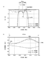
図8に示すように、C0=0.63pFのときは、規格化frを99.2%以下または102.2%以上とすることで、f2pが2×Passの外側に位置するようになる。同様に、C0=1.26pFでは、規格化frを99.4%以下または102.3%以上とする。C0=3.14pFでは、規格化frを99.6%以下または102.5%以上とする。f2p=5000MHzで最も大きい規格化frおよびf2p=5140MHzで最も小さい規格化frを太線で示す。規格化frを99.6%以下または102.2%以上とすると、全てのC0においてf2pが2×Pass内に位置しなくなる。 As shown in FIG. 8, when C0 = 0.63 pF, the normalized fr is set to 99.2% or less or 102.2% or more so that f2p is positioned outside 2 × Pass. Similarly, at C0 = 1.26 pF, the normalized fr is set to 99.4% or less or 102.3% or more. At C0 = 3.14 pF, the normalized fr is set to 99.6% or less or 102.5% or more. The thickest standardized fr at f2p = 5000 MHz and the smallest standardized fr at f2p = 5140 MHz are indicated by bold lines. When the regulations Kakuka fr to 99.6% or less, or 102.2% or more, f2p in all C0 not located within 2 × Pass.
図11(b)に示すように、共振周波数frxが通過帯域付近では、2次高調波SHD1、SHD2およびSHDpが劣化する。これは、図6のように、共振回路20により生成される2次高調波が周波数帯域2×Pass付近に位置するためである。共振周波数frxを2510MHz以下または2610MHz以上とすると、2次高調波SHD1、SHD2およびSHDの全てが−25dBm以下となる。
As shown in FIG. 11B, when the resonance frequency frx is in the vicinity of the pass band, the second harmonics SHD1, SHD2, and SHDp deteriorate. This is because the second harmonic generated by the
Claims (11)
前記入力端子と前記出力端子との間に並列に接続された1または複数の並列共振器と、
前記出力端子に最も近い直列共振器に並列に接続されたインダクタと、
を具備するフィルタ。 One or more including a series resonator that is connected in series between the input terminal and the output terminal, and that has a resonance frequency closest to the output terminal that is 99.6% or less or 102.2% or more of the center frequency of the passband A series resonator of
One or more parallel resonators connected in parallel between the input terminal and the output terminal;
An inductor connected in parallel to a series resonator closest to the output terminal;
A filter comprising:
前記出力端子に最も近い直列共振器の共振周波数は、前記複数の直列共振器の共振周波数のうち最も高いまたは最も低い請求項1から3のいずれか一項記載のフィルタ。 The one or more series resonators are a plurality of series resonators;
4. The filter according to claim 1, wherein a resonance frequency of the series resonator closest to the output terminal is the highest or the lowest among the resonance frequencies of the plurality of series resonators.
前記複数の直列共振器のうち少なくとも1つの直列共振器には並列にインダクタが接続されていない請求項1から4のいずれか一項記載のフィルタ。 The one or more series resonators are a plurality of series resonators;
The filter according to any one of claims 1 to 4, wherein an inductor is not connected in parallel to at least one of the plurality of series resonators.
前記入力端子と前記出力端子との間に並列に接続された1または複数の並列共振器と、
前記出力端子に最も近い直列共振器に並列に接続され、前記最も出力端子側の直列共振器とで通過帯域の2倍の周波数帯域内に位置する減衰極を形成するインダクタと、
を具備するフィルタ。 A plurality of series resonators including a series resonator connected in series between the input terminal and the output terminal and including the series resonator closest to the output terminal having the highest or lowest resonance frequency among the plurality of series resonators;
One or more parallel resonators connected in parallel between the input terminal and the output terminal;
An inductor connected in parallel to the series resonator closest to the output terminal, and forming an attenuation pole located in a frequency band twice the pass band with the series resonator closest to the output terminal;
A filter comprising:
Priority Applications (2)
| Application Number | Priority Date | Filing Date | Title |
|---|---|---|---|
| JP2016123980A JP6556668B2 (en) | 2016-06-22 | 2016-06-22 | Filters and multiplexers |
| US15/610,996 US10505516B2 (en) | 2016-06-22 | 2017-06-01 | Filter and multiplexer |
Applications Claiming Priority (1)
| Application Number | Priority Date | Filing Date | Title |
|---|---|---|---|
| JP2016123980A JP6556668B2 (en) | 2016-06-22 | 2016-06-22 | Filters and multiplexers |
Publications (3)
| Publication Number | Publication Date |
|---|---|
| JP2017228946A JP2017228946A (en) | 2017-12-28 |
| JP2017228946A5 true JP2017228946A5 (en) | 2018-03-22 |
| JP6556668B2 JP6556668B2 (en) | 2019-08-07 |
Family
ID=60677996
Family Applications (1)
| Application Number | Title | Priority Date | Filing Date |
|---|---|---|---|
| JP2016123980A Active JP6556668B2 (en) | 2016-06-22 | 2016-06-22 | Filters and multiplexers |
Country Status (2)
| Country | Link |
|---|---|
| US (1) | US10505516B2 (en) |
| JP (1) | JP6556668B2 (en) |
Families Citing this family (8)
| Publication number | Priority date | Publication date | Assignee | Title |
|---|---|---|---|---|
| US9800363B2 (en) * | 2014-06-18 | 2017-10-24 | Qualcomm Incorporated | NAICS signaling for advanced LTE features |
| JP6669132B2 (en) * | 2017-06-23 | 2020-03-18 | 株式会社村田製作所 | Multiplexer, transmitting device and receiving device |
| JP2019193220A (en) * | 2018-04-27 | 2019-10-31 | サムソン エレクトロ−メカニックス カンパニーリミテッド. | Filter including bulk acoustic wave resonator |
| JP2020053966A (en) * | 2018-09-24 | 2020-04-02 | スカイワークス グローバル プライベート リミテッド | Multilayer bulge frame in bulk elastic wave device |
| CN109831177A (en) * | 2018-12-20 | 2019-05-31 | 天津大学 | A kind of more stop-band filters and its implementation |
| JP6900947B2 (en) * | 2018-12-28 | 2021-07-14 | 株式会社村田製作所 | High frequency module and communication equipment |
| JP7352855B2 (en) * | 2019-08-21 | 2023-09-29 | 株式会社村田製作所 | duplexer |
| WO2023113003A1 (en) * | 2021-12-15 | 2023-06-22 | 株式会社村田製作所 | Elastic wave device and composite filter device |
Family Cites Families (9)
| Publication number | Priority date | Publication date | Assignee | Title |
|---|---|---|---|---|
| DE102005028927B4 (en) | 2005-06-22 | 2007-02-15 | Infineon Technologies Ag | BAW device |
| JP2007074698A (en) * | 2005-08-08 | 2007-03-22 | Fujitsu Media Device Kk | Duplexer and ladder type filter |
| JP5036435B2 (en) | 2006-09-01 | 2012-09-26 | 太陽誘電株式会社 | Elastic wave device, filter and duplexer |
| US7548140B2 (en) | 2007-04-16 | 2009-06-16 | Avago Technologies General Ip (Singapore) Pte. Ltd. | Bulk acoustic wave (BAW) filter having reduced second harmonic generation and method of reducing second harmonic generation in a BAW filter |
| WO2010061477A1 (en) * | 2008-11-28 | 2010-06-03 | 富士通株式会社 | Filter, duplexer and electronic device |
| JP5901101B2 (en) * | 2010-02-25 | 2016-04-06 | 太陽誘電株式会社 | Filter, duplexer, communication module, communication device |
| JP5873307B2 (en) * | 2011-11-21 | 2016-03-01 | 太陽誘電株式会社 | Filters and duplexers |
| US9419585B2 (en) * | 2013-08-22 | 2016-08-16 | Murata Manufacturing Co., Ltd. | Elastic wave filter device and duplexer |
| JP5613813B2 (en) * | 2013-10-17 | 2014-10-29 | 太陽誘電株式会社 | Duplexer |
-
2016
- 2016-06-22 JP JP2016123980A patent/JP6556668B2/en active Active
-
2017
- 2017-06-01 US US15/610,996 patent/US10505516B2/en active Active
Similar Documents
| Publication | Publication Date | Title |
|---|---|---|
| JP2017228946A5 (en) | ||
| US10355667B2 (en) | Ladder filter, elastic wave filter module, and duplexer | |
| JP6323348B2 (en) | Filter device | |
| US9419585B2 (en) | Elastic wave filter device and duplexer | |
| JP5237138B2 (en) | Filters, duplexers, communication modules | |
| JP2020014206A5 (en) | Hybrid elastic LC filters, multiplexers, and wireless communication devices with harmonic suppression | |
| CN107210731A (en) | Ladder type filter and duplexer | |
| WO2009025055A1 (en) | Elastic wave filter, duplexer using the elastic wave filter, and communication equipment using the duplexer | |
| US9680444B2 (en) | Multiplexer with filters and resonant circuit | |
| US10505516B2 (en) | Filter and multiplexer | |
| JP2010062816A (en) | Acoustic wave filter | |
| US9979375B2 (en) | Multi-harmonic matching networks | |
| JP2019507988A (en) | Use of filter parts and filter parts | |
| JP2021500838A5 (en) | ||
| CN107210732A (en) | Composite filter device | |
| JPWO2012176508A1 (en) | Duplexer | |
| CN106416068B (en) | Acoustic wave device | |
| JPWO2018096799A1 (en) | Filter device and multiplexer | |
| JP6411288B2 (en) | Ladder filters, duplexers and modules | |
| JP5459452B1 (en) | Filter device and duplexer | |
| JP5613813B2 (en) | Duplexer | |
| WO2018037884A1 (en) | Acoustic wave device | |
| WO2016031391A1 (en) | Ladder filter and duplexer | |
| KR101919115B1 (en) | Filter for using by bulk acoustic wave resonator | |
| WO2021213040A1 (en) | Resonance circuit and filtering device |