JP2017204635A - Semiconductor device package and manufacturing method of the same - Google Patents
Semiconductor device package and manufacturing method of the same Download PDFInfo
- Publication number
- JP2017204635A JP2017204635A JP2017091536A JP2017091536A JP2017204635A JP 2017204635 A JP2017204635 A JP 2017204635A JP 2017091536 A JP2017091536 A JP 2017091536A JP 2017091536 A JP2017091536 A JP 2017091536A JP 2017204635 A JP2017204635 A JP 2017204635A
- Authority
- JP
- Japan
- Prior art keywords
- conductive
- isolation layer
- layer
- pad
- semiconductor device
- Prior art date
- Legal status (The legal status is an assumption and is not a legal conclusion. Google has not performed a legal analysis and makes no representation as to the accuracy of the status listed.)
- Granted
Links
Images


Classifications
-
- H—ELECTRICITY
- H10—SEMICONDUCTOR DEVICES; ELECTRIC SOLID-STATE DEVICES NOT OTHERWISE PROVIDED FOR
- H10W—GENERIC PACKAGES, INTERCONNECTIONS, CONNECTORS OR OTHER CONSTRUCTIONAL DETAILS OF DEVICES COVERED BY CLASS H10
- H10W70/00—Package substrates; Interposers; Redistribution layers [RDL]
- H10W70/01—Manufacture or treatment
- H10W70/05—Manufacture or treatment of insulating or insulated package substrates, or of interposers, or of redistribution layers
- H10W70/093—Connecting or disconnecting other interconnections thereto or therefrom, e.g. connecting bond wires or bumps
-
- H—ELECTRICITY
- H10—SEMICONDUCTOR DEVICES; ELECTRIC SOLID-STATE DEVICES NOT OTHERWISE PROVIDED FOR
- H10W—GENERIC PACKAGES, INTERCONNECTIONS, CONNECTORS OR OTHER CONSTRUCTIONAL DETAILS OF DEVICES COVERED BY CLASS H10
- H10W70/00—Package substrates; Interposers; Redistribution layers [RDL]
- H10W70/01—Manufacture or treatment
- H10W70/05—Manufacture or treatment of insulating or insulated package substrates, or of interposers, or of redistribution layers
- H10W70/08—Manufacture or treatment of insulating or insulated package substrates, or of interposers, or of redistribution layers by depositing layers on the chip or wafer, e.g. "chip-first" RDLs
- H10W70/09—Manufacture or treatment of insulating or insulated package substrates, or of interposers, or of redistribution layers by depositing layers on the chip or wafer, e.g. "chip-first" RDLs extending onto an encapsulation that laterally surrounds the chip or wafer, e.g. fan-out wafer level package [FOWLP] RDLs
-
- H—ELECTRICITY
- H10—SEMICONDUCTOR DEVICES; ELECTRIC SOLID-STATE DEVICES NOT OTHERWISE PROVIDED FOR
- H10W—GENERIC PACKAGES, INTERCONNECTIONS, CONNECTORS OR OTHER CONSTRUCTIONAL DETAILS OF DEVICES COVERED BY CLASS H10
- H10W70/00—Package substrates; Interposers; Redistribution layers [RDL]
- H10W70/60—Insulating or insulated package substrates; Interposers; Redistribution layers
-
- H—ELECTRICITY
- H10—SEMICONDUCTOR DEVICES; ELECTRIC SOLID-STATE DEVICES NOT OTHERWISE PROVIDED FOR
- H10W—GENERIC PACKAGES, INTERCONNECTIONS, CONNECTORS OR OTHER CONSTRUCTIONAL DETAILS OF DEVICES COVERED BY CLASS H10
- H10W90/00—Package configurations
-
- H—ELECTRICITY
- H10—SEMICONDUCTOR DEVICES; ELECTRIC SOLID-STATE DEVICES NOT OTHERWISE PROVIDED FOR
- H10W—GENERIC PACKAGES, INTERCONNECTIONS, CONNECTORS OR OTHER CONSTRUCTIONAL DETAILS OF DEVICES COVERED BY CLASS H10
- H10W90/00—Package configurations
- H10W90/701—Package configurations characterised by the relative positions of pads or connectors relative to package parts
-
- H—ELECTRICITY
- H05—ELECTRIC TECHNIQUES NOT OTHERWISE PROVIDED FOR
- H05K—PRINTED CIRCUITS; CASINGS OR CONSTRUCTIONAL DETAILS OF ELECTRIC APPARATUS; MANUFACTURE OF ASSEMBLAGES OF ELECTRICAL COMPONENTS
- H05K1/00—Printed circuits
- H05K1/02—Details
- H05K1/14—Structural association of two or more printed circuits
- H05K1/144—Stacked arrangements of planar printed circuit boards
-
- H—ELECTRICITY
- H05—ELECTRIC TECHNIQUES NOT OTHERWISE PROVIDED FOR
- H05K—PRINTED CIRCUITS; CASINGS OR CONSTRUCTIONAL DETAILS OF ELECTRIC APPARATUS; MANUFACTURE OF ASSEMBLAGES OF ELECTRICAL COMPONENTS
- H05K2203/00—Indexing scheme relating to apparatus or processes for manufacturing printed circuits covered by H05K3/00
- H05K2203/13—Moulding and encapsulation; Deposition techniques; Protective layers
- H05K2203/1305—Moulding and encapsulation
- H05K2203/1316—Moulded encapsulation of mounted components
-
- H—ELECTRICITY
- H05—ELECTRIC TECHNIQUES NOT OTHERWISE PROVIDED FOR
- H05K—PRINTED CIRCUITS; CASINGS OR CONSTRUCTIONAL DETAILS OF ELECTRIC APPARATUS; MANUFACTURE OF ASSEMBLAGES OF ELECTRICAL COMPONENTS
- H05K3/00—Apparatus or processes for manufacturing printed circuits
- H05K3/22—Secondary treatment of printed circuits
- H05K3/28—Applying non-metallic protective coatings
- H05K3/284—Applying non-metallic protective coatings for encapsulating mounted components
-
- H—ELECTRICITY
- H10—SEMICONDUCTOR DEVICES; ELECTRIC SOLID-STATE DEVICES NOT OTHERWISE PROVIDED FOR
- H10W—GENERIC PACKAGES, INTERCONNECTIONS, CONNECTORS OR OTHER CONSTRUCTIONAL DETAILS OF DEVICES COVERED BY CLASS H10
- H10W70/00—Package substrates; Interposers; Redistribution layers [RDL]
- H10W70/01—Manufacture or treatment
- H10W70/05—Manufacture or treatment of insulating or insulated package substrates, or of interposers, or of redistribution layers
- H10W70/095—Manufacture or treatment of insulating or insulated package substrates, or of interposers, or of redistribution layers of vias therein
-
- H—ELECTRICITY
- H10—SEMICONDUCTOR DEVICES; ELECTRIC SOLID-STATE DEVICES NOT OTHERWISE PROVIDED FOR
- H10W—GENERIC PACKAGES, INTERCONNECTIONS, CONNECTORS OR OTHER CONSTRUCTIONAL DETAILS OF DEVICES COVERED BY CLASS H10
- H10W70/00—Package substrates; Interposers; Redistribution layers [RDL]
- H10W70/60—Insulating or insulated package substrates; Interposers; Redistribution layers
- H10W70/611—Insulating or insulated package substrates; Interposers; Redistribution layers for connecting multiple chips together
-
- H—ELECTRICITY
- H10—SEMICONDUCTOR DEVICES; ELECTRIC SOLID-STATE DEVICES NOT OTHERWISE PROVIDED FOR
- H10W—GENERIC PACKAGES, INTERCONNECTIONS, CONNECTORS OR OTHER CONSTRUCTIONAL DETAILS OF DEVICES COVERED BY CLASS H10
- H10W70/00—Package substrates; Interposers; Redistribution layers [RDL]
- H10W70/60—Insulating or insulated package substrates; Interposers; Redistribution layers
- H10W70/62—Insulating or insulated package substrates; Interposers; Redistribution layers characterised by their interconnections
- H10W70/63—Vias, e.g. via plugs
- H10W70/635—Through-vias
-
- H—ELECTRICITY
- H10—SEMICONDUCTOR DEVICES; ELECTRIC SOLID-STATE DEVICES NOT OTHERWISE PROVIDED FOR
- H10W—GENERIC PACKAGES, INTERCONNECTIONS, CONNECTORS OR OTHER CONSTRUCTIONAL DETAILS OF DEVICES COVERED BY CLASS H10
- H10W70/00—Package substrates; Interposers; Redistribution layers [RDL]
- H10W70/60—Insulating or insulated package substrates; Interposers; Redistribution layers
- H10W70/62—Insulating or insulated package substrates; Interposers; Redistribution layers characterised by their interconnections
- H10W70/65—Shapes or dispositions of interconnections
- H10W70/652—Cross-sectional shapes
- H10W70/6523—Cross-sectional shapes for connecting to pads at different heights at the same side of the package substrate, interposer or RDL
-
- H—ELECTRICITY
- H10—SEMICONDUCTOR DEVICES; ELECTRIC SOLID-STATE DEVICES NOT OTHERWISE PROVIDED FOR
- H10W—GENERIC PACKAGES, INTERCONNECTIONS, CONNECTORS OR OTHER CONSTRUCTIONAL DETAILS OF DEVICES COVERED BY CLASS H10
- H10W72/00—Interconnections or connectors in packages
- H10W72/01—Manufacture or treatment
- H10W72/012—Manufacture or treatment of bump connectors, dummy bumps or thermal bumps
- H10W72/01204—Manufacture or treatment of bump connectors, dummy bumps or thermal bumps using temporary auxiliary members, e.g. using sacrificial coatings or handle substrates
-
- H—ELECTRICITY
- H10—SEMICONDUCTOR DEVICES; ELECTRIC SOLID-STATE DEVICES NOT OTHERWISE PROVIDED FOR
- H10W—GENERIC PACKAGES, INTERCONNECTIONS, CONNECTORS OR OTHER CONSTRUCTIONAL DETAILS OF DEVICES COVERED BY CLASS H10
- H10W72/00—Interconnections or connectors in packages
- H10W72/01—Manufacture or treatment
- H10W72/012—Manufacture or treatment of bump connectors, dummy bumps or thermal bumps
- H10W72/01221—Manufacture or treatment of bump connectors, dummy bumps or thermal bumps using local deposition
- H10W72/01223—Manufacture or treatment of bump connectors, dummy bumps or thermal bumps using local deposition in liquid form, e.g. by dispensing droplets or by screen printing
-
- H—ELECTRICITY
- H10—SEMICONDUCTOR DEVICES; ELECTRIC SOLID-STATE DEVICES NOT OTHERWISE PROVIDED FOR
- H10W—GENERIC PACKAGES, INTERCONNECTIONS, CONNECTORS OR OTHER CONSTRUCTIONAL DETAILS OF DEVICES COVERED BY CLASS H10
- H10W72/00—Interconnections or connectors in packages
- H10W72/01—Manufacture or treatment
- H10W72/012—Manufacture or treatment of bump connectors, dummy bumps or thermal bumps
- H10W72/01221—Manufacture or treatment of bump connectors, dummy bumps or thermal bumps using local deposition
- H10W72/01225—Manufacture or treatment of bump connectors, dummy bumps or thermal bumps using local deposition in solid form, e.g. by using a powder or by stud bumping
-
- H—ELECTRICITY
- H10—SEMICONDUCTOR DEVICES; ELECTRIC SOLID-STATE DEVICES NOT OTHERWISE PROVIDED FOR
- H10W—GENERIC PACKAGES, INTERCONNECTIONS, CONNECTORS OR OTHER CONSTRUCTIONAL DETAILS OF DEVICES COVERED BY CLASS H10
- H10W72/00—Interconnections or connectors in packages
- H10W72/01—Manufacture or treatment
- H10W72/0198—Manufacture or treatment batch processes
-
- H—ELECTRICITY
- H10—SEMICONDUCTOR DEVICES; ELECTRIC SOLID-STATE DEVICES NOT OTHERWISE PROVIDED FOR
- H10W—GENERIC PACKAGES, INTERCONNECTIONS, CONNECTORS OR OTHER CONSTRUCTIONAL DETAILS OF DEVICES COVERED BY CLASS H10
- H10W72/00—Interconnections or connectors in packages
- H10W72/071—Connecting or disconnecting
- H10W72/073—Connecting or disconnecting of die-attach connectors
- H10W72/07302—Connecting or disconnecting of die-attach connectors using an auxiliary member
- H10W72/07304—Connecting or disconnecting of die-attach connectors using an auxiliary member the auxiliary member being temporary, e.g. a sacrificial coating
- H10W72/07307—Connecting or disconnecting of die-attach connectors using an auxiliary member the auxiliary member being temporary, e.g. a sacrificial coating the auxiliary member being a temporary substrate, e.g. a removable substrate
-
- H—ELECTRICITY
- H10—SEMICONDUCTOR DEVICES; ELECTRIC SOLID-STATE DEVICES NOT OTHERWISE PROVIDED FOR
- H10W—GENERIC PACKAGES, INTERCONNECTIONS, CONNECTORS OR OTHER CONSTRUCTIONAL DETAILS OF DEVICES COVERED BY CLASS H10
- H10W72/00—Interconnections or connectors in packages
- H10W72/20—Bump connectors, e.g. solder bumps or copper pillars; Dummy bumps; Thermal bumps
- H10W72/221—Structures or relative sizes
- H10W72/225—Bumps having a filler embedded in a matrix
-
- H—ELECTRICITY
- H10—SEMICONDUCTOR DEVICES; ELECTRIC SOLID-STATE DEVICES NOT OTHERWISE PROVIDED FOR
- H10W—GENERIC PACKAGES, INTERCONNECTIONS, CONNECTORS OR OTHER CONSTRUCTIONAL DETAILS OF DEVICES COVERED BY CLASS H10
- H10W72/00—Interconnections or connectors in packages
- H10W72/20—Bump connectors, e.g. solder bumps or copper pillars; Dummy bumps; Thermal bumps
- H10W72/221—Structures or relative sizes
- H10W72/227—Multiple bumps having different sizes
-
- H—ELECTRICITY
- H10—SEMICONDUCTOR DEVICES; ELECTRIC SOLID-STATE DEVICES NOT OTHERWISE PROVIDED FOR
- H10W—GENERIC PACKAGES, INTERCONNECTIONS, CONNECTORS OR OTHER CONSTRUCTIONAL DETAILS OF DEVICES COVERED BY CLASS H10
- H10W72/00—Interconnections or connectors in packages
- H10W72/20—Bump connectors, e.g. solder bumps or copper pillars; Dummy bumps; Thermal bumps
- H10W72/231—Shapes
- H10W72/234—Cross-sectional shape, i.e. in side view
-
- H—ELECTRICITY
- H10—SEMICONDUCTOR DEVICES; ELECTRIC SOLID-STATE DEVICES NOT OTHERWISE PROVIDED FOR
- H10W—GENERIC PACKAGES, INTERCONNECTIONS, CONNECTORS OR OTHER CONSTRUCTIONAL DETAILS OF DEVICES COVERED BY CLASS H10
- H10W72/00—Interconnections or connectors in packages
- H10W72/20—Bump connectors, e.g. solder bumps or copper pillars; Dummy bumps; Thermal bumps
- H10W72/241—Dispositions, e.g. layouts
- H10W72/242—Dispositions, e.g. layouts relative to the surface, e.g. recessed, protruding
-
- H—ELECTRICITY
- H10—SEMICONDUCTOR DEVICES; ELECTRIC SOLID-STATE DEVICES NOT OTHERWISE PROVIDED FOR
- H10W—GENERIC PACKAGES, INTERCONNECTIONS, CONNECTORS OR OTHER CONSTRUCTIONAL DETAILS OF DEVICES COVERED BY CLASS H10
- H10W72/00—Interconnections or connectors in packages
- H10W72/20—Bump connectors, e.g. solder bumps or copper pillars; Dummy bumps; Thermal bumps
- H10W72/241—Dispositions, e.g. layouts
- H10W72/244—Dispositions, e.g. layouts relative to underlying supporting features, e.g. bond pads, RDLs or vias
-
- H—ELECTRICITY
- H10—SEMICONDUCTOR DEVICES; ELECTRIC SOLID-STATE DEVICES NOT OTHERWISE PROVIDED FOR
- H10W—GENERIC PACKAGES, INTERCONNECTIONS, CONNECTORS OR OTHER CONSTRUCTIONAL DETAILS OF DEVICES COVERED BY CLASS H10
- H10W72/00—Interconnections or connectors in packages
- H10W72/20—Bump connectors, e.g. solder bumps or copper pillars; Dummy bumps; Thermal bumps
- H10W72/251—Materials
- H10W72/252—Materials comprising solid metals or solid metalloids, e.g. PbSn, Ag or Cu
-
- H—ELECTRICITY
- H10—SEMICONDUCTOR DEVICES; ELECTRIC SOLID-STATE DEVICES NOT OTHERWISE PROVIDED FOR
- H10W—GENERIC PACKAGES, INTERCONNECTIONS, CONNECTORS OR OTHER CONSTRUCTIONAL DETAILS OF DEVICES COVERED BY CLASS H10
- H10W72/00—Interconnections or connectors in packages
- H10W72/20—Bump connectors, e.g. solder bumps or copper pillars; Dummy bumps; Thermal bumps
- H10W72/251—Materials
- H10W72/253—Materials not comprising solid metals or solid metalloids, e.g. polymers or ceramics
-
- H—ELECTRICITY
- H10—SEMICONDUCTOR DEVICES; ELECTRIC SOLID-STATE DEVICES NOT OTHERWISE PROVIDED FOR
- H10W—GENERIC PACKAGES, INTERCONNECTIONS, CONNECTORS OR OTHER CONSTRUCTIONAL DETAILS OF DEVICES COVERED BY CLASS H10
- H10W72/00—Interconnections or connectors in packages
- H10W72/823—Interconnections through encapsulations, e.g. pillars through molded resin on a lateral side a chip
-
- H—ELECTRICITY
- H10—SEMICONDUCTOR DEVICES; ELECTRIC SOLID-STATE DEVICES NOT OTHERWISE PROVIDED FOR
- H10W—GENERIC PACKAGES, INTERCONNECTIONS, CONNECTORS OR OTHER CONSTRUCTIONAL DETAILS OF DEVICES COVERED BY CLASS H10
- H10W72/00—Interconnections or connectors in packages
- H10W72/851—Dispositions of multiple connectors or interconnections
- H10W72/874—On different surfaces
- H10W72/884—Die-attach connectors and bond wires
-
- H—ELECTRICITY
- H10—SEMICONDUCTOR DEVICES; ELECTRIC SOLID-STATE DEVICES NOT OTHERWISE PROVIDED FOR
- H10W—GENERIC PACKAGES, INTERCONNECTIONS, CONNECTORS OR OTHER CONSTRUCTIONAL DETAILS OF DEVICES COVERED BY CLASS H10
- H10W72/00—Interconnections or connectors in packages
- H10W72/90—Bond pads, in general
- H10W72/921—Structures or relative sizes of bond pads
- H10W72/923—Bond pads having multiple stacked layers
-
- H—ELECTRICITY
- H10—SEMICONDUCTOR DEVICES; ELECTRIC SOLID-STATE DEVICES NOT OTHERWISE PROVIDED FOR
- H10W—GENERIC PACKAGES, INTERCONNECTIONS, CONNECTORS OR OTHER CONSTRUCTIONAL DETAILS OF DEVICES COVERED BY CLASS H10
- H10W72/00—Interconnections or connectors in packages
- H10W72/90—Bond pads, in general
- H10W72/931—Shapes of bond pads
- H10W72/932—Plan-view shape, i.e. in top view
-
- H—ELECTRICITY
- H10—SEMICONDUCTOR DEVICES; ELECTRIC SOLID-STATE DEVICES NOT OTHERWISE PROVIDED FOR
- H10W—GENERIC PACKAGES, INTERCONNECTIONS, CONNECTORS OR OTHER CONSTRUCTIONAL DETAILS OF DEVICES COVERED BY CLASS H10
- H10W72/00—Interconnections or connectors in packages
- H10W72/90—Bond pads, in general
- H10W72/931—Shapes of bond pads
- H10W72/934—Cross-sectional shape, i.e. in side view
-
- H—ELECTRICITY
- H10—SEMICONDUCTOR DEVICES; ELECTRIC SOLID-STATE DEVICES NOT OTHERWISE PROVIDED FOR
- H10W—GENERIC PACKAGES, INTERCONNECTIONS, CONNECTORS OR OTHER CONSTRUCTIONAL DETAILS OF DEVICES COVERED BY CLASS H10
- H10W72/00—Interconnections or connectors in packages
- H10W72/90—Bond pads, in general
- H10W72/941—Dispositions of bond pads
- H10W72/9413—Dispositions of bond pads on encapsulations
-
- H—ELECTRICITY
- H10—SEMICONDUCTOR DEVICES; ELECTRIC SOLID-STATE DEVICES NOT OTHERWISE PROVIDED FOR
- H10W—GENERIC PACKAGES, INTERCONNECTIONS, CONNECTORS OR OTHER CONSTRUCTIONAL DETAILS OF DEVICES COVERED BY CLASS H10
- H10W72/00—Interconnections or connectors in packages
- H10W72/90—Bond pads, in general
- H10W72/941—Dispositions of bond pads
- H10W72/942—Dispositions of bond pads relative to underlying supporting features, e.g. bond pads, RDLs or vias
-
- H—ELECTRICITY
- H10—SEMICONDUCTOR DEVICES; ELECTRIC SOLID-STATE DEVICES NOT OTHERWISE PROVIDED FOR
- H10W—GENERIC PACKAGES, INTERCONNECTIONS, CONNECTORS OR OTHER CONSTRUCTIONAL DETAILS OF DEVICES COVERED BY CLASS H10
- H10W72/00—Interconnections or connectors in packages
- H10W72/90—Bond pads, in general
- H10W72/981—Auxiliary members, e.g. spacers
- H10W72/985—Alignment aids, e.g. alignment marks
-
- H—ELECTRICITY
- H10—SEMICONDUCTOR DEVICES; ELECTRIC SOLID-STATE DEVICES NOT OTHERWISE PROVIDED FOR
- H10W—GENERIC PACKAGES, INTERCONNECTIONS, CONNECTORS OR OTHER CONSTRUCTIONAL DETAILS OF DEVICES COVERED BY CLASS H10
- H10W72/00—Interconnections or connectors in packages
- H10W72/90—Bond pads, in general
- H10W72/981—Auxiliary members, e.g. spacers
- H10W72/987—Flow barriers
-
- H—ELECTRICITY
- H10—SEMICONDUCTOR DEVICES; ELECTRIC SOLID-STATE DEVICES NOT OTHERWISE PROVIDED FOR
- H10W—GENERIC PACKAGES, INTERCONNECTIONS, CONNECTORS OR OTHER CONSTRUCTIONAL DETAILS OF DEVICES COVERED BY CLASS H10
- H10W74/00—Encapsulations, e.g. protective coatings
- H10W74/10—Encapsulations, e.g. protective coatings characterised by their shape or disposition
- H10W74/111—Encapsulations, e.g. protective coatings characterised by their shape or disposition the semiconductor body being completely enclosed
- H10W74/114—Encapsulations, e.g. protective coatings characterised by their shape or disposition the semiconductor body being completely enclosed by a substrate and the encapsulations
- H10W74/117—Encapsulations, e.g. protective coatings characterised by their shape or disposition the semiconductor body being completely enclosed by a substrate and the encapsulations the substrate having spherical bumps for external connection
-
- H—ELECTRICITY
- H10—SEMICONDUCTOR DEVICES; ELECTRIC SOLID-STATE DEVICES NOT OTHERWISE PROVIDED FOR
- H10W—GENERIC PACKAGES, INTERCONNECTIONS, CONNECTORS OR OTHER CONSTRUCTIONAL DETAILS OF DEVICES COVERED BY CLASS H10
- H10W74/00—Encapsulations, e.g. protective coatings
- H10W74/10—Encapsulations, e.g. protective coatings characterised by their shape or disposition
- H10W74/131—Encapsulations, e.g. protective coatings characterised by their shape or disposition the semiconductor body being only partially enclosed
- H10W74/142—Encapsulations, e.g. protective coatings characterised by their shape or disposition the semiconductor body being only partially enclosed the encapsulations exposing the passive side of the semiconductor body
-
- H—ELECTRICITY
- H10—SEMICONDUCTOR DEVICES; ELECTRIC SOLID-STATE DEVICES NOT OTHERWISE PROVIDED FOR
- H10W—GENERIC PACKAGES, INTERCONNECTIONS, CONNECTORS OR OTHER CONSTRUCTIONAL DETAILS OF DEVICES COVERED BY CLASS H10
- H10W74/00—Encapsulations, e.g. protective coatings
- H10W74/10—Encapsulations, e.g. protective coatings characterised by their shape or disposition
- H10W74/15—Encapsulations, e.g. protective coatings characterised by their shape or disposition on active surfaces of flip-chip devices, e.g. underfills
-
- H—ELECTRICITY
- H10—SEMICONDUCTOR DEVICES; ELECTRIC SOLID-STATE DEVICES NOT OTHERWISE PROVIDED FOR
- H10W—GENERIC PACKAGES, INTERCONNECTIONS, CONNECTORS OR OTHER CONSTRUCTIONAL DETAILS OF DEVICES COVERED BY CLASS H10
- H10W90/00—Package configurations
- H10W90/20—Configurations of stacked chips
- H10W90/22—Configurations of stacked chips the stacked chips being on both top and bottom sides of a package substrate, interposer or RDL
-
- H—ELECTRICITY
- H10—SEMICONDUCTOR DEVICES; ELECTRIC SOLID-STATE DEVICES NOT OTHERWISE PROVIDED FOR
- H10W—GENERIC PACKAGES, INTERCONNECTIONS, CONNECTORS OR OTHER CONSTRUCTIONAL DETAILS OF DEVICES COVERED BY CLASS H10
- H10W90/00—Package configurations
- H10W90/20—Configurations of stacked chips
- H10W90/24—Configurations of stacked chips at least one of the stacked chips being laterally offset from a neighbouring stacked chip, e.g. chip stacks having a staircase shape
-
- H—ELECTRICITY
- H10—SEMICONDUCTOR DEVICES; ELECTRIC SOLID-STATE DEVICES NOT OTHERWISE PROVIDED FOR
- H10W—GENERIC PACKAGES, INTERCONNECTIONS, CONNECTORS OR OTHER CONSTRUCTIONAL DETAILS OF DEVICES COVERED BY CLASS H10
- H10W90/00—Package configurations
- H10W90/20—Configurations of stacked chips
- H10W90/291—Configurations of stacked chips characterised by containers, encapsulations, or other housings for the stacked chips
-
- H—ELECTRICITY
- H10—SEMICONDUCTOR DEVICES; ELECTRIC SOLID-STATE DEVICES NOT OTHERWISE PROVIDED FOR
- H10W—GENERIC PACKAGES, INTERCONNECTIONS, CONNECTORS OR OTHER CONSTRUCTIONAL DETAILS OF DEVICES COVERED BY CLASS H10
- H10W90/00—Package configurations
- H10W90/401—Package configurations characterised by multiple insulating or insulated package substrates, interposers or RDLs
-
- H—ELECTRICITY
- H10—SEMICONDUCTOR DEVICES; ELECTRIC SOLID-STATE DEVICES NOT OTHERWISE PROVIDED FOR
- H10W—GENERIC PACKAGES, INTERCONNECTIONS, CONNECTORS OR OTHER CONSTRUCTIONAL DETAILS OF DEVICES COVERED BY CLASS H10
- H10W90/00—Package configurations
- H10W90/701—Package configurations characterised by the relative positions of pads or connectors relative to package parts
- H10W90/721—Package configurations characterised by the relative positions of pads or connectors relative to package parts of bump connectors
- H10W90/722—Package configurations characterised by the relative positions of pads or connectors relative to package parts of bump connectors between stacked chips
-
- H—ELECTRICITY
- H10—SEMICONDUCTOR DEVICES; ELECTRIC SOLID-STATE DEVICES NOT OTHERWISE PROVIDED FOR
- H10W—GENERIC PACKAGES, INTERCONNECTIONS, CONNECTORS OR OTHER CONSTRUCTIONAL DETAILS OF DEVICES COVERED BY CLASS H10
- H10W90/00—Package configurations
- H10W90/701—Package configurations characterised by the relative positions of pads or connectors relative to package parts
- H10W90/721—Package configurations characterised by the relative positions of pads or connectors relative to package parts of bump connectors
- H10W90/724—Package configurations characterised by the relative positions of pads or connectors relative to package parts of bump connectors between a chip and a stacked insulating package substrate, interposer or RDL
-
- H—ELECTRICITY
- H10—SEMICONDUCTOR DEVICES; ELECTRIC SOLID-STATE DEVICES NOT OTHERWISE PROVIDED FOR
- H10W—GENERIC PACKAGES, INTERCONNECTIONS, CONNECTORS OR OTHER CONSTRUCTIONAL DETAILS OF DEVICES COVERED BY CLASS H10
- H10W90/00—Package configurations
- H10W90/701—Package configurations characterised by the relative positions of pads or connectors relative to package parts
- H10W90/731—Package configurations characterised by the relative positions of pads or connectors relative to package parts of die-attach connectors
- H10W90/732—Package configurations characterised by the relative positions of pads or connectors relative to package parts of die-attach connectors between stacked chips
-
- H—ELECTRICITY
- H10—SEMICONDUCTOR DEVICES; ELECTRIC SOLID-STATE DEVICES NOT OTHERWISE PROVIDED FOR
- H10W—GENERIC PACKAGES, INTERCONNECTIONS, CONNECTORS OR OTHER CONSTRUCTIONAL DETAILS OF DEVICES COVERED BY CLASS H10
- H10W90/00—Package configurations
- H10W90/701—Package configurations characterised by the relative positions of pads or connectors relative to package parts
- H10W90/731—Package configurations characterised by the relative positions of pads or connectors relative to package parts of die-attach connectors
- H10W90/734—Package configurations characterised by the relative positions of pads or connectors relative to package parts of die-attach connectors between a chip and a stacked insulating package substrate, interposer or RDL
-
- H—ELECTRICITY
- H10—SEMICONDUCTOR DEVICES; ELECTRIC SOLID-STATE DEVICES NOT OTHERWISE PROVIDED FOR
- H10W—GENERIC PACKAGES, INTERCONNECTIONS, CONNECTORS OR OTHER CONSTRUCTIONAL DETAILS OF DEVICES COVERED BY CLASS H10
- H10W90/00—Package configurations
- H10W90/701—Package configurations characterised by the relative positions of pads or connectors relative to package parts
- H10W90/751—Package configurations characterised by the relative positions of pads or connectors relative to package parts of bond wires
- H10W90/754—Package configurations characterised by the relative positions of pads or connectors relative to package parts of bond wires between a chip and a stacked insulating package substrate, interposer or RDL
-
- H—ELECTRICITY
- H10—SEMICONDUCTOR DEVICES; ELECTRIC SOLID-STATE DEVICES NOT OTHERWISE PROVIDED FOR
- H10W—GENERIC PACKAGES, INTERCONNECTIONS, CONNECTORS OR OTHER CONSTRUCTIONAL DETAILS OF DEVICES COVERED BY CLASS H10
- H10W99/00—Subject matter not provided for in other groups of this subclass
Landscapes
- Internal Circuitry In Semiconductor Integrated Circuit Devices (AREA)
- Structures Or Materials For Encapsulating Or Coating Semiconductor Devices Or Solid State Devices (AREA)
- Engineering & Computer Science (AREA)
- Manufacturing & Machinery (AREA)
Abstract
【課題】流動している半田ペーストにより移動されない銅ポストを有する半導体パッケージを提供する。【解決手段】半導体パッケージ10は、キャリア100と、パッド104と、第1の隔離層106と、相互接続層108と、導電性ポストを110備える。キャリアは、第1の表面101及び第1の表面と対向する第2の表面を有する。パッドは、キャリアの第1の表面に第1の部分と第2の部分を有する。第1の隔離層は、第1の表面の上に配置され、パッドの第1の部分を被覆し、上面を有する。相互接続層は、パッドの第2の部分の上に配置され、上面を有する。導電性ポストは、第1の隔離層の上面の上と相互接続層の上面の上に配置される。第1の隔離層の上面と相互接続層の上面は、実質的に同一の平面にある。【選択図】図1AA semiconductor package having a copper post that is not moved by a flowing solder paste. A semiconductor package includes a carrier, a pad, a first isolation layer, an interconnect layer, and a conductive post. The carrier has a first surface 101 and a second surface opposite the first surface. The pad has a first portion and a second portion on the first surface of the carrier. The first isolation layer is disposed on the first surface, covers the first portion of the pad, and has an upper surface. The interconnect layer is disposed on the second portion of the pad and has a top surface. Conductive posts are disposed on the top surface of the first isolation layer and on the top surface of the interconnect layer. The top surface of the first isolation layer and the top surface of the interconnect layer are in substantially the same plane. [Selection] Figure 1A
Description
[関連出願]
本出願は、2016年6月20日に出願された米国特許出願62/352,299号と、2016年5月11日に出願された米国特許出願62/334,861号を基礎出願とする優先権を享受する。本出願はこれらの基礎出願を参照することによって基礎出願の全ての内容を含む。
[技術分野]
[Related applications]
This application enjoys priority based on US patent application 62 / 352,299 filed June 20, 2016 and US patent application 62 / 334,861 filed May 11, 2016. . This application includes the entire contents of the basic applications by reference to these basic applications.
[Technical field]
本発明は、半導体装置パッケージ及びその製造方法に関する。特に、本発明は、同時に半田ペースト及び半田レジストに配置される銅ポストに関する。 The present invention relates to a semiconductor device package and a manufacturing method thereof. In particular, the present invention relates to a copper post that is simultaneously placed on a solder paste and a solder resist.
一部の半導体パッケージ(例えば、パッケージ-オン-パッケージ(PoP)工法により形成された)には、半田ボールは、外部接続又は相互接続に用いられる。しかし、半田ボールのピッチの長さは、小型化を阻害する可能性がある。その代わりに、ファインピッチの銅(Cu)ポスト工法は、小型化に使用されることがある。このような工法の手法の一つは、パッシベーション層にホールを形成してCuポストを受けることである。しかし、Cuポストのピッチが相対的に小さいので、ホールへのCuポストのインプランテーションは困難である。このような工法のピッチは、加工ツールの性能により制限されることがある。もう一つの手法では、Cuポストを導電性パッドに配置して次の操作を行う。このような手法において、Cuポストは、直接に半田ペースト(例えば、導電性パッド)に配置され、半田ペーストの面積がCuポストより大きい。還流の操作には、(加熱される時に流動し得る)溶融された半田ペーストは、Cuポストを支持しない可能性がある。これらの状況で、Cuポストは、流動している半田ペーストにより移動される場合がある。 In some semiconductor packages (eg, formed by a package-on-package (PoP) method), solder balls are used for external connections or interconnections. However, the pitch length of the solder balls may hinder downsizing. Instead, the fine pitch copper (Cu) post method may be used for miniaturization. One such technique is to form a hole in the passivation layer and receive a Cu post. However, since the pitch of the Cu posts is relatively small, it is difficult to implant the Cu posts into the holes. The pitch of such a method may be limited by the performance of the processing tool. In another method, a Cu post is placed on a conductive pad and the following operation is performed. In such a method, the Cu post is directly disposed on a solder paste (for example, a conductive pad), and the area of the solder paste is larger than that of the Cu post. For the reflux operation, the molten solder paste (which can flow when heated) may not support the Cu post. Under these circumstances, the Cu post may be moved by the flowing solder paste.
ある実施形態において、一つの態様によれば、半導体パッケージは、第1の表面及び第1の表面と対向する第2の表面を有する基板と、第1の部分及び第2の部分を含み、基板の第1の表面の上に配置されるパッドと、第1の表面の上に配置され、パッドの第1の部分を被覆し、上面を有する第1の隔離層と、パッドの第2の部分の上に配置され、上面を有する相互接続層と、第1の隔離層の上面の上と相互接続層の上面の上に配置される導電性ポストを備える。第1の隔離層の上面と相互接続層の上面は、実質的に同一の平面にある。 In one embodiment, according to one aspect, a semiconductor package includes a substrate having a first surface and a second surface opposite the first surface, and a first portion and a second portion, A pad disposed on the first surface of the first surface, a first isolation layer disposed on the first surface, covering the first portion of the pad and having an upper surface, and a second portion of the pad And an interconnect layer having a top surface and a conductive post disposed on the top surface of the first isolation layer and on the top surface of the interconnect layer. The top surface of the first isolation layer and the top surface of the interconnect layer are in substantially the same plane.
ある実施形態において、他の態様によれば、半導体パッケージは、第1の表面及び第1の表面と対向する第2の表面を有する基板と、基板の第1の表面の上に配置され、第1の部分と、第2の部分と、第3の部分を含む導電性パッドと、導電性パッドの第1の部分の上に配置される第1の隔離層と、パッドの第2の部分の上に配置され、上面を有する相互接続層と、パッドの第3の部分の上に配置される第2の隔離層と、相互接続層の上と第1の隔離層の上に配置される導電性ポストを備える。相互接続層の上面と第1の隔離層の上面は、実質的に同一の平面にある。 In certain embodiments, according to another aspect, a semiconductor package is disposed on the first surface of the substrate, the substrate having the first surface and the second surface opposite the first surface, and A conductive pad including a first portion, a second portion, a third portion, a first isolation layer disposed over the first portion of the conductive pad, and a second portion of the pad An interconnect layer disposed on and having a top surface; a second isolation layer disposed on the third portion of the pad; and a conductive layer disposed on the interconnect layer and on the first isolation layer. With sex posts. The top surface of the interconnect layer and the top surface of the first isolation layer are substantially in the same plane.
ある実施形態において、他の態様によれば、半導体装置パッケージを製造する方法は、第1の表面に第1の表面及び第1の表面と対向する第2の表面を有する基板と、第1の部分及び第2の部分を有する導電性パッドを提供することと、導電性パッドの第1の部分を被覆するように、上面を有する第1の隔離層を形成することと、上面を有する導電層を導電層の第2の部分の上に配置することと、導電性素子を第1の隔離層の上面と導電層の上面の上に配置することと、を含む。第1の隔離層の上面と導電層の上面は、実質的に同一の平面にある。 In one embodiment, according to another aspect, a method of manufacturing a semiconductor device package includes a first surface having a first surface and a substrate having a second surface opposite the first surface; Providing a conductive pad having a portion and a second portion; forming a first isolation layer having a top surface so as to cover the first portion of the conductive pad; and a conductive layer having a top surface Disposing on the second portion of the conductive layer and disposing the conductive element on the top surface of the first isolation layer and on the top surface of the conductive layer. The upper surface of the first isolation layer and the upper surface of the conductive layer are substantially in the same plane.
図面と詳しい説明では、同一又は同様な部材には同一の符号を付す。本発明の実施形態は、添付図面と以下の詳細な説明により容易に理解される。 In the drawings and detailed description, the same or similar members are denoted by the same reference numerals. Embodiments of the present invention will be readily understood by the accompanying drawings and the following detailed description.
関連する図面に示される部材の配向について、「上」、「下」、「上」、「左」、「右」、「下」、「頂部」、「底部」、「垂直」、「水平」、「側面」、「より高い」、「より低い」、「上部」、「の上」、「の下」のような空間の説明は、所定の部材又は部材群、或いは部材又は部材群の所定の平面に対して特定されている。ここで使用される空間の説明は、例示的なものであり、本発明の実施形態の利点から逸脱しない限り、ここで説明された構造の実施は、任意の配向又は方式で空間的に配置可能であることが理解される。 Regarding the orientation of the members shown in the related drawings, “top”, “bottom”, “top”, “left”, “right”, “bottom”, “top”, “bottom”, “vertical”, “horizontal” , “Side”, “higher”, “lower”, “upper”, “above”, “below” are described for a given member or group of members, or for a given member or group of members. Specific to the plane. The description of the space used here is exemplary and the implementation of the structure described herein can be spatially arranged in any orientation or manner without departing from the advantages of the embodiments of the present invention. It is understood that
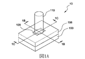
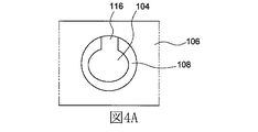
図1Aは、本発明のある実施形態による半導体装置パッケージ10の斜視図である。半導体装置パッケージ10は、キャリア100と、パッド104(図1Aに図示せず)と、隔離層106と、相互接続層108と、導電性ポスト110を備える。隔離層106は、パッド104を部分的に被覆する。隔離層106は、パッド104の少なくとも一部を露出させる開口を区画する。隔離層106により被覆されずに露出したパッド104の部分は、実質的な矩形又は実質的な正方形形状をしてもよい。他の実施形態において、パッド104は、実質的な円形又は実質的な楕円形状などの他の形状をしてもよい。導電性ポスト110は、隔離層106と相互接続層108に配置される。ある実施形態において、相互接続層108の外縁の形状は、実質的な矩形又は実質的な正方形であってもよい。
FIG. 1A is a perspective view of a
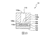
図1Bは、本発明のある実施形態による半導体装置パッケージ10の図1Aに示す切断線1Bに沿った断面図である。
FIG. 1B is a cross-sectional view of
キャリア100は、表面101及び表面101と対向する表面102を有する。ここで説明するある実施形態において、キャリア100の表面101は、上面又は第1の表面と呼ばれ、基板の表面102は、底面又は第2の表面と呼ばれる。キャリア100は、例えば、紙基の銅箔積層板、複合銅箔積層板、又はポリマー含浸ガラスファイバー基の銅箔積層板などのプリント配線板であってもよく、或いはこのようなプリント配線板を含んでもよい。キャリア100は、再分布層(RDL)又は接地素子などの相互接続構造を含んでもよい。ある実施形態において、接地素子は、キャリア100の側面から露出したビアである。ある実施形態において、接地素子は、キャリア100の側面から露出した金属層である。ある実施形態において、接地素子は、キャリア100の側面から露出した金属トレースである。
The
パッド104は、キャリア100の表面101に配置される。隔離層106は、キャリア100の表面101に配置され、パッド104の第1の部分を被覆する。パッド104の第2の部分は、隔離層106から露出する。相互接続層108は、パッド104の露出した部分において、隔離層106により区画された開口の上に形成される。ある実施形態において、開口の面積は、およそ0.0125平方ミリメートル(mm2)(例えば、およそ0.05mm×およそ0.25mmの長さを有する辺により区画された)〜およそ0.08mm2(例えば、およそ0.2mm×およそ0.4mmの長さを有する辺により区画された)の範囲にある。相互接続層108は、パッド104に配置され、隔離層106により取り囲まれる。隔離層106は、上面106aを有する。隔離層106は、パシベーション材、樹脂、又はポリマーなどの半田レジストであってもよい。相互接続層108は、上面108aを有する。相互接続層108は、Sn(錫)及び/又は他の適切な金属材料から形成されるか、或いはそれらを含む。相互接続層108の体積及び/又は重量は、適切に設定される。導電性ポスト110は、隔離層106の上面106aと相互接続層108の上面108aに配置される。ある実施形態において、導電性ポスト110の幅(例えば、図1Bに図示される水平方向における延伸)は、およそ0.15mm〜およそ0.3mmの範囲にある。ある実施形態において、導電性ポスト110は、実質的な円筒形状をなし、導電性ポスト110の径は、およそ0.15mm〜およそ0.3mmの範囲にある。ある実施形態において、図1Aに示すように、導電性ポスト110の第1の径は、第1の方向に沿って伸びて、隔離層106ではなく相互接続層108にわたって伸びるが、第1の径と同じ平面にある導電性ポスト110の第2の径は、第1の方向に直交する第2の方向に沿って伸びて、部分的に相互接続層108にわたって伸び、さらに部分的に隔離層106にわたって伸びる。換言すれば、導電性ポスト110の径に対応する第1の仮想線は、隔離層106ではなく相互接続層108にわたって伸びるように描画される(例えば、図1Aに示す線1C‐1Cに沿って描画される)が、導電性ポスト110の径にも対応する第2の仮想線は、第1の仮想線と異なる方向に描画され、相互接続層108と隔離層106の両方にわたって伸びる(例えば、図1Aに示す線1B-1Bに沿う)。隔離層106の上面106aと相互接続層108の上面108aは、実質的に同一の平面にある。
The
導電性ポスト110は、第1部と第2部を有する底面110bを含む。導電性ポスト110の底面110bの第1部は、相互接続層108の上面108aに接触し、導電性ポスト110の底面110bの第2部は、隔離層106の上面106aに接触する。導電性ポスト110の底面110bの第1部の面積は、実質的に導電性ポスト110の底面110bの第2部の面積に等しい又はそれよりも大きい。導電性ポスト110は、Cu及び/又は他の適切な金属材料から形成される。隔離層106と導電性ポスト110は、モールド化合物112により包まれる。ある実施形態において、導電性ポスト110は、実質的に還流操作において最初の位置を保持し、少なくとも部分的に導電性ポスト110が隔離層106により支持されているため、導電性ポスト110の位置は、溶融された相互接続層108の流動により大きく影響されていない。
The
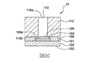
図1Cは、本発明のある実施形態による切断線1Cに沿った半導体装置パッケージ10の断面図である。
FIG. 1C is a cross-sectional view of the
隔離層106は、キャリア100の表面101に配置される。隔離層106は、キャリア100の表面101に配置され、部分的にパッド104の第1の部分を被覆する。パッド104の第2の部分は、隔離層106から露出する。相互接続層108は、パッド104に配置されて隔離層106で取り囲まれる。導電性ポスト110は、相互接続層108に配置される。隔離層106の上面106aと相互接続層108の上面108aは、実質的に同一の平面にある。
The
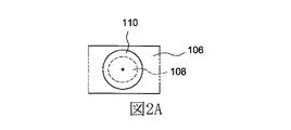
図2Aは、本発明のある実施形態による半導体装置パッケージ10における導電性ポスト110のレイアウトを示す。隔離層106は、部分的にパッド104を被覆して、パッド104の一部を隔離層106から露出させる。露出したパッド104の部分は、円形形状をする。ある実施形態において、円形の露出した部分の径は、およそ0.05mm〜およそ0.2mmの範囲にある。相互接続層108は、パッド104の露出した部分に配置される。相互接続層108の形状は、円形である。導電性ポスト110は、隔離層106と相互接続層108に配置され、実質的に隔離層106により支持される。相互接続層108は、実質的に導電性ポスト110により完全に被覆される。相互接続層108と導電性ポスト110は、実質的な同心円を形成する。ある実施形態において、導電性ポスト110の径は、およそ0.15mm〜およそ0.3mmの範囲にある。
FIG. 2A shows a layout of
図2Bは、本発明のある実施形態による半導体装置パッケージ10における導電性ポスト110のレイアウトを示す。図2Bのレイアウトは、図2Aに類似している。パッド104を露出させる、隔離層106により区画された開口は、円形形状をなす。相互接続層108は、パッド104の露出した部分に形成される。相互接続層108の形状は、円形である。導電性ポスト110は、隔離層106と相互接続層108に配置され、実質的に隔離層106により支持される。相互接続層108は、実質的に導電性ポスト110により完全に被覆される。相互接続層108の一部の縁は、導電性ポスト110の一部の縁と重なり合う。導電性ポスト110の中心は、相互接続層108の中心から離れる。
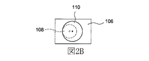
FIG. 2B shows a layout of the
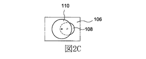
図2Cは、本発明のある実施形態による半導体装置パッケージ10における導電性ポスト110のレイアウトを示す。図2Cのレイアウトは、図2Bに類似している。相互接続層108の形状は、円形である。導電性ポスト110は、隔離層106と相互接続層108に配置され、実質的に隔離層106により支持される。相互接続層108は、部分的に導電性ポスト110により被覆される。導電性ポスト110の中心は、相互接続層108の中心から離れる。
FIG. 2C illustrates a layout of the
図3Aは、本発明のある実施形態による半導体装置パッケージ20の斜視図である。半導体装置パッケージ20の構造は、半導体装置パッケージ10に類似している。半導体装置パッケージ20は、キャリア200と、隔離層206と、相互接続層208と、導電性ポスト210と、モールド化合物212とを備える。ある実施形態において、相互接続層208の形状は、円形である。相互接続層208は、還流操作において収縮し得る。還流操作の後、モールド化合物212を半導体装置パッケージ20に適用してパッド204(例えば、図3Cに示すように)と、隔離層206と、相互接続層208と導電性ポスト210を包んでもよい。
FIG. 3A is a perspective view of a
ある実施形態において、相互接続層208をパッド204に配置してから、導電性ポスト210を相互接続層208に配置する。ある実施形態において、相互接続層208を導電性ポスト210に追加してから、導電性ポスト210と相互接続層208をパッド204に配置する。したがって、ある実施形態において、複数の導電性ポストの間のピッチは、必ずツールの性能によって制限されず(例えば、狭ピッチの構造では、必ず半導体装置パッケージに追加した相互接続層に導電性ポスト210を形成するツールの性能によって制限されず)、フレキシビリティーが向上する。
In some embodiments, the
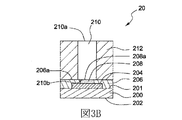
図3Bは、本発明のある実施形態による切断線2Bに沿った半導体装置パッケージ20の断面図である。キャリア200は、上面201及び上面201と対向する底面202を有する。隔離層206は、上面206aを有する。パッド204は、キャリア200の上面201に配置される。隔離層206は、キャリア200の上面201に配置され、部分的にパッド204を被覆する。相互接続層208は、上面208aを有する。図1Bの構造と同様に、導電性ポスト210は、上面210aと底面210bを含み、隔離層206の上面206aと相互接続層208の上面208aに配置される。隔離層206の上面206aと相互接続層208の上面208aは、実質的に同一の平面にある。導電性ポスト210の底面210bは、第1部と第2部を有する。第1部は、相互接続層208の上面208aに接触し、第2部は、第1の隔離層206の上面206aに接触する。導電性ポスト210の底面210bの第1部の面積は、導電性ポスト210の底面210bの第2部の面積に実質的に等しい又はそれよりも大きい。
FIG. 3B is a cross-sectional view of
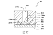
図3Cは、本発明のある実施形態による切断線2Cに沿った半導体装置パッケージ20の断面図である。相互接続層208の体積及び/又は重量は、適切に設定され、相互接続層208の上面208aの面積は、適切に設定される。ある実施形態において、相互接続層208は、実質的な円形形状をなし、相互接続層208の径は、およそ0.05mm〜およそ0.2mmの範囲にある。相互接続層208は、還流操作中に収縮して隔離層206と相互接続層208の間におけるギャップを生成又は増大することができる。ギャップは、モールド化合物212で充填されてもよい。モールド化合物212は、パッド204と、隔離層206と、相互接続層208と、導電性ポスト210のそれぞれに接触する。モールド化合物212は、パッド204と、隔離層206と、相互接続層208と、導電性ポスト210のそれぞれを包む。
FIG. 3C is a cross-sectional view of
ある実施形態において、パッド204は、第1の部分と、第2の部分と、第3の部分を有する。隔離層206は、パッド204の第1の部分を被覆する。相互接続層208は、パッド204の第2の部分に接触し、それを被覆する。モールド化合物212は、パッドの第3の部分に接触し、それを被覆する。ある実施形態において、導電性ポスト210は、実質的に還流操作において最初の位置を保持し、少なくとも部分的に導電性ポスト210が隔離層206とモールド化合物212により支持されているため、導電性ポスト210の位置は、溶融された相互接続層208の流動により大きく影響されていない。
In some embodiments, the
図4Aは、本発明のある実施形態による半導体装置パッケージ10におけるパッド104のレイアウトを示す。隔離層106は、キャリア100に配置される。隔離層106は、開口を区画する。パッド104とトレース116は、開口に形成される。隔離層106は、パッド104とトレース116を取り囲む。トレース116の一端は、隔離層106に接触してもよい。相互接続層108は、開口に形成される。相互接続層108は、完全にパッド104とトレース116を被覆する。
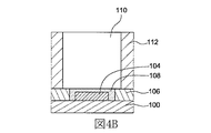
FIG. 4A shows a layout of
図4Bは、本発明のある実施形態による半導体装置パッケージ10の断面図である。隔離層106は、キャリア100に形成される。パッド104は、キャリア100に形成される。相互接続層108は、キャリア10に形成され、完全にパッド104を被覆する。隔離層106の上面と相互接続層108の上面は、同一の平面にある。導電性ポスト110は、隔離層106と相互接続層108に配置され、実質的に隔離層106により支持される。隔離層106と導電性ポスト110は、モールド化合物112で包まれる。
FIG. 4B is a cross-sectional view of a
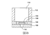
図5Aは、本発明のある実施形態による半導体装置パッケージ10におけるパッド104のレイアウトを示す。図5Aのレイアウトは、図4Aに類似している。隔離層106は、キャリア100に形成される。隔離層106は、開口を区画する。パッド104は、キャリア100と付加されたビア118(図5Bに示す)に形成される。パッド104と開口は、同心円を形成する。
FIG. 5A shows a layout of
図5Bは、本発明のある実施形態による半導体装置パッケージ10の断面図である。図5Bの構造は、図4Bに類似している。付加されたビア118は、キャリア100に形成される。付加されたビア118は、パッド104と、相互接続層108と、導電性ポスト110に電気的に接続される。
FIG. 5B is a cross-sectional view of a
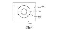
図6Aは、本発明のある実施形態による半導体装置パッケージ10における導電性ポスト110のレイアウトを図示する。パッド104は、部分的に隔離層106により被覆される。隔離層106により区画された開口は、円形形状をなし、パッド104の一部を露出させる。相互接続層108は、開口に形成される。相互接続層108は、パッド104に配置される。導電性ポスト110は、隔離層106と相互接続層108に配置され、実質的に隔離層106により支持される。パッド104、隔離層106、相互接続層108、及び導電性ポスト110を包む空間は、モールド化合物112で充填されてもよい。ある実施形態において、導電性ポスト110の寸法は、およそ180μm〜およそ220μmの範囲にある。例えば、導電性ポスト110の寸法は、およそ200μmである。
FIG. 6A illustrates a layout of
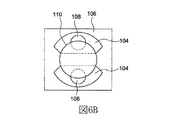
図6Bは、本発明のある実施形態による半導体装置パッケージ10における導電性ポスト110のレイアウトを図示する。パッド104は、部分的に隔離層106により被覆される。二つの独立した開口は、隔離層106により区画され、パッド104を露出させる。ある実施形態において、開口は、実質的に台形形状である。ある実施形態において、開口は、実質的にポリゴン形状である。ある実施形態において、開口は、第1の方向(例えば、図6Bに示す水平方向)に伸びる第1の直線と第1の直線に向かって第1の方向に第1の直線を越えて伸びる凸状の円弧により区画された形状をなし、円弧の各々の端が、それぞれ第2の直線と第3の直線により第1の直線の各々の端に接続される。二つの相互接続層108は、それぞれ開口に形成される。導電性ポスト110は、隔離層106と相互接続層108に配置され、実質的に隔離層106により支持される。パッド104、隔離層106、相互接続層108、及び導電性ポスト110を包む空間は、モールド化合物112で充填されてもよい。ある実施形態において、導電性ポスト110は、円筒形状であり、導電性ポスト110の径は、およそ180μm〜およそ220μmの範囲にある。例えば、導電性ポスト110の径は、およそ200μmである。ある実施形態において、少なくとも一つの開口の湾曲した外縁と、同じ平面にある導電性ポスト110の外縁との径方向における距離は、およそ40μm〜およそ60μmの範囲にある。例えば、径方向の距離は、およそ50μmである。
FIG. 6B illustrates the layout of the
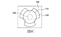
図6Cは、本発明のある実施形態による半導体装置パッケージ10における導電性ポスト110のレイアウトを図示する。パッド104は、部分的に隔離層106により被覆される。パッド104を露出させる、隔離層106により区画された開口は、完全でない円形形状をなす。例えば、開口は、図6Cに示すように、実質的に三つの円形部がこれらの円形部を含む仮想円の中心部に一体的に接続される形状をしてもよい。相互接続層108は、開口に形成される。導電性ポスト110は、隔離層106と相互接続層108に配置され、実質的に隔離層106により支持される。パッド104、隔離層106、相互接続層108、及び導電性ポスト110を包む空間は、モールド化合物112で充填してもよい。例えば、相互接続層108は、大体開口の中心に形成される。ある実施形態において、導電性ポスト110は、円筒形状であり、導電性ポスト110の径は、およそ180μm〜およそ220μmの範囲にある。例えば、導電性ポスト110の径は、およそ200μmである。ある実施形態において、少なくとも一つの開口の湾曲した外縁と、同じ平面にある導電性ポスト110の外縁との径方向における距離は、およそ40μm〜およそ60μmの範囲にある。例えば、径方向の距離は、およそ50μmである。
FIG. 6C illustrates the layout of the
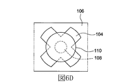
図6Dは、本発明のある実施形態による半導体装置パッケージ10における導電性ポスト110のレイアウトを図示する。図示されたレイアウトは、隔離層106により区画された開口が実質的にX形状である以外に、図6Cに図示されたレイアウトと同様である。
FIG. 6D illustrates the layout of the
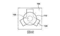
図6Eは、本発明のある実施形態による半導体装置パッケージ10における導電性ポスト110のレイアウトを図示する。図示されたレイアウトは、隔離層106により区画された開口が実質的にY形状である以外に、図6Dに図示されたレイアウトと同様である。
FIG. 6E illustrates the layout of the
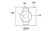
図6Fは、本発明のある実施形態による半導体装置パッケージ10における導電性ポスト110のレイアウトを図示する。図示されたレイアウトは、隔離層106により区画された開口が実質的に矩形形状である以外に、図6Aに図示されたレイアウトと同様である。ある実施形態において、開口の短辺と、同じ平面にある導電性ポスト110の外縁との間の距離は、およそ40μm〜およそ60μmの範囲にある。例えば、径方向の距離は、およそ50μmである。
FIG. 6F illustrates the layout of the
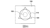
図6Gは、本発明のある実施形態による半導体装置パッケージ10における導電性ポスト110のレイアウトを図示する。図示されたレイアウトは、隔離層106により区画された開口が実質的に三角形状である以外に、図6Aに図示されたレイアウトと同様である。ある実施形態において、三角形状の開口の一つの角と、同じ平面にある導電性ポスト110の外縁との間の距離は、およそ40μm〜およそ60μmの範囲にある。例えば、径方向の距離は、およそ50μmである。
FIG. 6G illustrates the layout of the
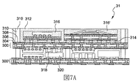
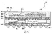
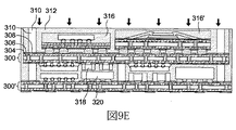
図7Aは、本発明のある実施形態による半導体装置パッケージ31の断面図である。半導体装置パッケージ31は、キャリア300と300'、パッド304、隔離層306、相互接続層308、導電性ポスト310、モールド化合物312、半田ボール314、パッケージ316と316'、及び装置318と320を含む。導電性ポスト310は、隔離層306と相互接続層308に配置される。隔離層306の上面と相互接続層308の上面は、実質的に同一の平面にある。パッケージ316と316'は、それぞれ一つ以上の個別の半田ボール314を介してキャリア300の前側(図7Aにおける上側)に配置される。モールド化合物312は、パッド304、隔離層306、導電性ポスト310、及びパッケージ316と316'を包む。装置318は、キャリア300の裏側(図7Aにおける底側)に配置される。導電性ポストは、キャリア300と300'の間に配置される。装置320は、キャリア300'の前側(図7Aにおける上側)に配置される。
FIG. 7A is a cross-sectional view of a
キャリア300は、キャリア300'と同じ又はキャリア300'に類似してもよい。キャリア300は、キャリア300'と異なってもよい。キャリア300は、例えば、紙基の銅箔積層板、複合銅箔積層板、又はポリマー含浸ガラスファイバー基の銅箔積層板などのプリント配線板であるか、或いはそれらを含む。キャリア300は、RDL又は接地素子などの相互接続構造を含んでもよい。ある実施形態において、接地素子は、キャリア300の側面から露出したビアである。ある実施形態において、接地素子は、キャリア300の側面から露出した金属層である。ある実施形態において、接地素子は、キャリア300の側面から露出した金属トレースである。
ある実施形態において、パッケージ316は、(例えば、フリップチップアセンブリに適する)フリップパッケージである。パッケージ316'は、ワイヤボンディングパッケージである。装置318は、受動装置である。装置320は、能動装置である。ある実施形態において、パッケージ316と316'及び装置318と320は、半導体装置パッケージの異なる設計によってキャリア300と300'の異なる位置に配置される。他のタイプのパッケージ及び/又は他の組合せ及び/又はコンフィグの装置であってもよい。
In certain embodiments,
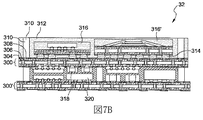
図7Bは、本発明のある実施形態による半導体装置パッケージ32の断面図である。半導体装置パッケージ32の構造は、半導体装置パッケージ31に類似している。半導体装置パッケージ32と半導体装置パッケージ31の相違点は、半導体装置パッケージ32において、キャリア300と300'の間に配置されるアンダーフィル樹脂があることである。
FIG. 7B is a cross-sectional view of a
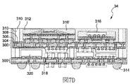
図7Cは、本発明のある実施形態による半導体装置パッケージ33の断面図である。半導体装置パッケージ33の構造は、半導体装置パッケージ31に類似している。半導体装置パッケージ33と半導体装置パッケージ31の相違点は、半導体装置パッケージ33において、さらにキャリア300と300'の間にモールド化合物を配置し、また、付加された半田ボールがキャリア300'の裏側に配置されることである。さらなるモールド化合物は、キャリア300'の前側に配置され、キャリア300、パッド304、隔離層306、導電性ポスト310、半田ボール314、パッケージ316と316'、及び装置318と320を包む。
FIG. 7C is a cross-sectional view of a
図7Dは、本発明のある実施形態による半導体装置パッケージ34の断面図である。半導体装置パッケージ34の構造は、半導体装置パッケージ33に類似している。半導体装置パッケージ34と半導体装置パッケージ33の相違点は、半導体装置パッケージ34において、少なくとも一つの付加された受動装置及び/又は少なくとも一つの付加された能動装置がキャリア300'の裏側に配置されることである。
FIG. 7D is a cross-sectional view of a
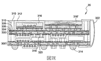
図7Eは、本発明のある実施形態による半導体装置パッケージ35の断面図である。半導体装置パッケージ35の構造は、半導体装置パッケージ34に類似している。半導体装置パッケージ35と半導体装置パッケージ34の相違点は、半導体装置パッケージ35において、相互接続素子322でキャリア300をキャリア300'に電気的に接続することである。
FIG. 7E is a cross-sectional view of a
図8A、図8B、図8C、図8D、図8E、図8F、及び図8Gは、本発明のある実施形態による半導体装置パッケージを製造する方法を示す。 8A, 8B, 8C, 8D, 8E, 8F, and 8G illustrate a method of manufacturing a semiconductor device package according to an embodiment of the present invention.
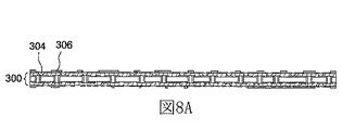
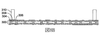
図8Aを参照して、半導体装置パッケージを製造する方法は、キャリア300を提供することを含む。キャリア300は、前側(図8Aにおける上側)と裏側(図8Aにおける底側)を有する。前側は、裏側と対向する。パッド304は、キャリア300の前側に配置される。隔離層306は、キャリア300の前側に配置され、部分的にパッド304を被覆することがある。隔離層306は、パッド304を露出させる一つ以上の開口を区画してもよい。
Referring to FIG. 8A, a method for manufacturing a semiconductor device package includes providing a
図8Bを参照して、導電性ポスト310は、隔離層306と相互接続層308に配置される。ある実施形態において、相互接続層308は、パッド304に配置され、次に、導電性ポスト310は、相互接続層308に配置される。もう一つの実施形態において、相互接続層308は、導電性ポスト310に取付けられ、次に、相互接続層308が取付けられた導電性ポスト310は、パッド304に配置される。
With reference to FIG. 8B,
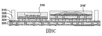
図8Cを参照して、一つ以上の半田ボール314は、パッド304に配置される。パッケージ316と316'は、半田ボール314を介してキャリア300の前側に配置される。ある実施形態において、パッケージ316と316'は、同じ種類のパッケージである。ある実施形態において、パッケージ316と316'は、異なる種類のパッケージである。
Referring to FIG. 8C, one or
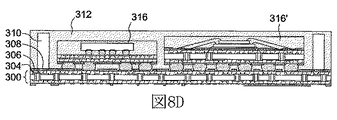
図8Dを参照して、モールド化合物312は、キャリア300の前側に配置される。モールド化合物312は、パッド304、隔離層306、導電性ポスト310、及びパッケージ316と316'を包む。
Referring to FIG. 8D, the
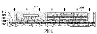
図8Eを参照して、モールド化合物312は、導電性ポスト310の上面を露出させるために研削される。
Referring to FIG. 8E, the
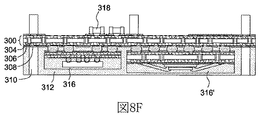
図8Fを参照して、付加された導電性ポストは、キャリア300の裏側に配置される。装置318は、キャリア300の裏側に配置される。
Referring to FIG. 8F, the added conductive post is disposed on the back side of the
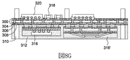
図8Gを参照して、装置320は、キャリア300の裏側に配置される。
Referring to FIG. 8G, the
図9A、図9B、図9C、図9D、図9E、及び図9Fは、本発明のある実施形態による半導体装置パッケージを製造する方法を示す。図9A、図9B、図9C、図9D、図9E、及び図9Fに図示される工程は、図8A、図8B、図8C、図8D、図8E、図8F、及び図8Gに図示される工程の後に実行されてもよいが、それに制限されていない。 9A, 9B, 9C, 9D, 9E, and 9F illustrate a method of manufacturing a semiconductor device package according to an embodiment of the present invention. The steps illustrated in FIGS. 9A, 9B, 9C, 9D, 9E, and 9F are illustrated in FIGS. 8A, 8B, 8C, 8D, 8E, 8F, and 8G. It may be performed after the process, but is not limited thereto.
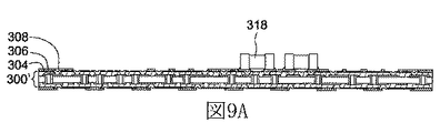
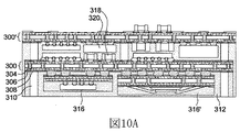
図9Aを参照して、半導体装置パッケージを製造する方法は、キャリア300'を提供することを含む。キャリア300'は、前側(図9Aにおける上側)と裏側(図9Aにおける底側)を有する。前側は、裏側と対向する。パッド304は、キャリア300'の前側に配置される。隔離層306は、キャリア300'の前側に配置され、部分的にパッド304を被覆することがある。装置318は、キャリア300'の前側に配置される。
With reference to FIG. 9A, a method of manufacturing a semiconductor device package includes providing a
図9Bを参照して、装置320は、キャリア300'の前側に配置される。
Referring to FIG. 9B, the
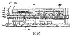
図9Cを参照して、図8Gに示すような構造は、キャリア300'の前側に配置される。
Referring to FIG. 9C, the structure as shown in FIG. 8G is disposed on the front side of the
図9Dを参照して、付加されたモールド化合物312は、キャリア300'の前側に適用される。付加されたモールド化合物312は、キャリア300、パッド304、隔離層306、導電性ポスト310、半田ボール314、パッケージ316と316'、及び装置318と320を包む。
Referring to FIG. 9D, the added
図9Eを参照して、付加されたモールド化合物312は、導電性ポスト310の上面を露出させるために研削される。
Referring to FIG. 9E, the added
図9Fを参照して、一つ以上の付加された半田ボールは、キャリア300'の裏側に配置される。
Referring to FIG. 9F, one or more added solder balls are disposed on the back side of the
図10A、図10B、図10C、図10D、及び図10Eは、本発明のある実施形態による半導体装置パッケージを製造する方法を示す。図10A、図10B、図10C、図10D、及び図10Eに図示される工程は、図9A、図9B、図9C、図9D、図9E、及び図9Fに図示される工程の後に実行されてもよいが、それに制限されていない。 10A, 10B, 10C, 10D, and 10E illustrate a method of manufacturing a semiconductor device package according to an embodiment of the present invention. The steps illustrated in FIGS. 10A, 10B, 10C, 10D, and 10E are performed after the steps illustrated in FIGS.9A, 9B, 9C, 9D, 9E, and 9F. It is good, but not limited to it.
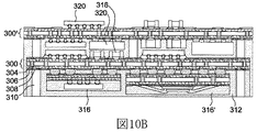
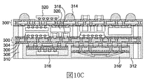
図10Aを参照して、図9Eに示すような構造が提供される。付加された装置318は、キャリア300'の裏側に配置される。
Referring to FIG. 10A, a structure as shown in FIG. 9E is provided. The added
図10Bを参照して、付加された装置320は、キャリア300'の裏側に配置される。
Referring to FIG. 10B, the added
図10Cを参照して、一つ以上の付加された半田ボール314は、キャリア300'の裏側に配置される。
Referring to FIG. 10C, one or more added
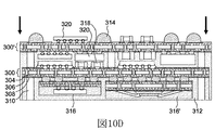
図10Dを参照して、単独の半導体装置パッケージを生成するために個片化操作が実行される。 Referring to FIG. 10D, a singulation operation is performed to generate a single semiconductor device package.
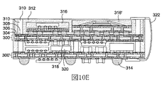
図10Eを参照して、相互接続素子322の一端は、モールド化合物312の上面に配置され、導電性ポスト310に接触し、相互接続素子322の他端は、キャリア300'の裏側に配置される。相互接続素子322は、キャリア300をキャリア300'に電気的に接続する。
Referring to FIG. 10E, one end of the
完成された半導体パッケージの厚さの減少を含むパッケージ寸法の減少を実現する貫通孔構造及び関連する製造工法の実施形態は、例によって本発明に説明されている。 Embodiments of through-hole structures and associated manufacturing methods that achieve package size reduction, including reduced thickness of the completed semiconductor package, are described in the present invention by way of example.
フリップチップボンディング工法は、より厚いダイによりダイのクラックを防ぐ。例えば、フリップチップボンディングにおいてクラックを防ぐために、研削の後、ダイの厚さは4ミリメートル(mm)以上であることが望ましい。 The flip chip bonding method prevents die cracking with a thicker die. For example, in order to prevent cracks in flip chip bonding, it is desirable that the die thickness be greater than 4 millimeters (mm) after grinding.
したがって、パッケージの総厚が懸念される構造に対して、フリップチップボンディングではなく、直接ダイボンディング工法が実行され、約2mmのダイ厚さで十分な製造歩留まりを達成する。 Therefore, a direct die bonding method is executed instead of flip chip bonding for a structure in which the total thickness of the package is a concern, and a sufficient manufacturing yield is achieved with a die thickness of about 2 mm.
なお、パッケージの総厚をさらに減少するために基板の厚さの減少を図ることが望ましい。 It is desirable to reduce the thickness of the substrate in order to further reduce the total thickness of the package.
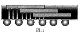
本発明の実施形態によれば、直接ダイボンディング工法とバンプ工法により、厚さが減少された基板に実行されてパッケージの総厚の減少を達成する。直接ダイボンディング工法とバンプ工法は、単一のダイパッケージ又は複数の(例えば、積み重ねられた)ダイパッケージに適する。本発明の実施形態によれば、三つの積み重ねられたダイを備えたパッケージに対して、約0.4mm以下のパッケージの総厚が達成される。 According to an embodiment of the present invention, a direct die bonding method and a bump method are performed on a substrate having a reduced thickness to achieve a reduction in the total thickness of the package. The direct die bonding method and bump method are suitable for a single die package or multiple (eg, stacked) die packages. According to embodiments of the present invention, a total package thickness of about 0.4 mm or less is achieved for a package with three stacked dies.
図11は、本発明の実施形態による半導体パッケージを示す。図11には、直接ダイボンディング工法とバンプ工法により、三つの積み重ねられたダイを備えたパッケージに対して、約0.4mm以下のパッケージの総厚を達成する。 FIG. 11 shows a semiconductor package according to an embodiment of the present invention. In FIG. 11, a total die thickness of about 0.4 mm or less is achieved for a package with three stacked dies by a direct die bonding method and a bump method.
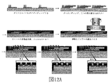
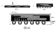
図12Aは、本発明の実施形態による半導体のパッケージ工法を示す。図12Aに示すように、ダミーウエハーが提供され、ダイが単位面積におけるダミーウエハー(次のステージにおいて各個の単位に分離される)に結着される。 FIG. 12A illustrates a semiconductor packaging method according to an embodiment of the present invention. As shown in FIG. 12A, a dummy wafer is provided and the die is bonded to a dummy wafer in a unit area (separated into individual units in the next stage).
また、図12Aを参照して、ピラーがダイに配置されるか、或いはダイボンディングの前に、ピラーを備えたダイが提供される。付加されたダイは、ダミーウエハーに結着されたダイにダイボンディングされ、付加されたピラーは、付加されたダイに配置される。図示されるように、三つのダイが積み重ねられるように互いに結着され、そのピラーがダイから垂直(図示された配向)に伸びる。三つ以上又は以下のダイがダイボンディングにより積み重ねられてもよい。ダイが積み重ねられた後、モールドがウエハーの周りに設けられ、封入材料がモールドに充填される。例えば、液体化合物がモールドに充填されて、積み重ねられたダイの周りに充填され、さらにダミーウエハーに流下する。 Referring also to FIG. 12A, a pillar with a pillar is provided before the pillar is placed on the die or prior to die bonding. The added die is die-bonded to the die bonded to the dummy wafer, and the added pillar is disposed on the added die. As shown, three dies are bonded together so that they are stacked, and their pillars extend vertically from the dies (the orientation shown). Three or more or less dies may be stacked by die bonding. After the dies are stacked, a mold is placed around the wafer and the encapsulant is filled into the mold. For example, a liquid compound is filled into a mold, filled around the stacked dies, and then flows down to a dummy wafer.
モールドが除去され、(硬化後の)封入材料が押し潰されて封入材料の表面にピラーを露出させる。 The mold is removed and the encapsulant (after curing) is crushed to expose the pillars on the surface of the encapsulant.
ポリイミドなどの絶縁層は、封入材料の表面の上に配置される。絶縁層は、各個のピラーを露出させるそれぞれの開口を区画する。そして、再分布層(RDL)は、絶縁層の上に開口の中に配置され、ピラーと電気的に接続される。もう一つの絶縁層、例えばポリイミドは、RDLの上に配置される。 An insulating layer such as polyimide is disposed on the surface of the encapsulating material. The insulating layer defines each opening that exposes each individual pillar. The redistribution layer (RDL) is disposed in the opening on the insulating layer and is electrically connected to the pillar. Another insulating layer, such as polyimide, is placed over the RDL.
図12Bは、次の製造ステージを示す。半田ボールは、RDLに配置される。半田ボールは、ピラーの上に位置するか、或いはピラーからずれて位置してもよい。したがって、半田ボールのピッチは、ピラーのピッチより大きくてもよい。 FIG. 12B shows the next manufacturing stage. Solder balls are placed on the RDL. The solder ball may be located on the pillar or may be offset from the pillar. Therefore, the pitch of the solder balls may be larger than the pitch of the pillars.
図12Bに示すように、半田ボールが配置された後、ダミーウエハーが押し潰される。ある実施形態において、ダミーウエハーは、研削しきれ、ダイスタックの一番上のダイを露出させる。 As shown in FIG. 12B, after the solder balls are arranged, the dummy wafer is crushed. In some embodiments, the dummy wafer can be ground to expose the top die of the die stack.
図12Cは、図12Cの「完成」に示すように、また、図11に示すように、単位面積が単一化されて各個の半導体パッケージに分離される次の製造ステージを示す。図12Cに示すように、完成された半導体パッケージの総厚は、約398マイクロメートル(μm)である。 FIG. 12C shows the next manufacturing stage as shown in “completion” of FIG. 12C and as shown in FIG. 11, the unit area is unified and separated into individual semiconductor packages. As shown in FIG. 12C, the total thickness of the completed semiconductor package is about 398 micrometers (μm).
図12Cにおける完成された半導体パッケージの総厚は、約175μmの半田ボールの高さと、約28μmのRDLの高さと、約195μmの封入材料の高さを含む。最長のピラーの高さは、約145μmで(示された配向に垂直である)、中間のピラーは、約85μmで、最短のピラーは、約25μmである。各々のダイは、約10μmと厚く、各々の絶縁層は、約9μmと厚く、RDLは、約5μmと厚く、積み重ねられた三つのダイの高さの合計が約50〜60μmである。 The total thickness of the completed semiconductor package in FIG. 12C includes a solder ball height of about 175 μm, an RDL height of about 28 μm, and an encapsulant height of about 195 μm. The height of the longest pillar is about 145 μm (perpendicular to the orientation shown), the middle pillar is about 85 μm, and the shortest pillar is about 25 μm. Each die is about 10 μm thick, each insulating layer is about 9 μm thick, RDL is about 5 μm thick, and the total height of the three stacked dies is about 50-60 μm.
ピラーは、銅であるか、或いは銅を含む。一つ以上の実施形態において、一つ以上のピラーは、各個のダイにめっきされる。一つ以上の実施形態において、一つ以上のピラーは、各個のダイにピンで実装される。ピラーは、同じ径をしてもよく、いくつかのピラーは、異なる径をしてもよい。 The pillar is copper or contains copper. In one or more embodiments, one or more pillars are plated on each individual die. In one or more embodiments, one or more pillars are mounted with pins on each individual die. The pillars may have the same diameter, and some pillars may have different diameters.
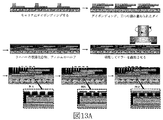
図13Aは、本発明の実施形態による半導体のパッケージ工法を示す。図13Aに示すように、ダミーキャリアが提供され、ダイが単位面積におけるキャリア(次のステージにおいて各個の単位に分離される)に結着される。 FIG. 13A illustrates a semiconductor packaging method according to an embodiment of the present invention. As shown in FIG. 13A, a dummy carrier is provided and the die is bound to a carrier in unit area (separated into individual units in the next stage).
また、図13Aを参照して、ピラーがダイに配置されるか、或いはダイボンディングの前に、ピラーを備えたダイが提供される。付加されたダイは、キャリアに結着されたダイにダイボンディングされ、付加されたピラーは、付加されたダイに配置される。図示されるように、三つのダイが積み重ねられるように互いに結着され、そのピラーがダイから垂直(図示された配向)に伸びる。三つ以上又は以下のダイがダイボンディングにより積み重ねられてもよい。ダイが積み重ねられた後、モールドがウエハーの周りに設けられ、封入材料がモールドに充填される。例えば、液体化合物がモールドに充填されて、積み重ねられたダイの周りに充填され、さらにキャリアに流下する。 Referring also to FIG. 13A, a pillar with a pillar is provided before the pillar is placed on the die or before die bonding. The added die is die-bonded to the die bonded to the carrier, and the added pillar is arranged on the added die. As shown, three dies are bonded together so that they are stacked, and their pillars extend vertically from the dies (the orientation shown). Three or more or less dies may be stacked by die bonding. After the dies are stacked, a mold is placed around the wafer and the encapsulant is filled into the mold. For example, a liquid compound is filled into a mold, filled around the stacked dies, and then flows down to the carrier.
モールドが除去され、(硬化後の)封入材料が押し潰されて封入材料の表面にピラーを露出させる。 The mold is removed and the encapsulant (after curing) is crushed to expose the pillars on the surface of the encapsulant.
ポリイミドなどの絶縁層は、封入材料の表面の上に配置される。絶縁層は、各個のピラーを露出させるそれぞれの開口を区画する。そして、再分布層(RDL)は、絶縁層の上に開口の中に配置され、ピラーと電気的に接続される。もう一つの絶縁層、例えばポリイミドは、RDLの上に配置される。 An insulating layer such as polyimide is disposed on the surface of the encapsulating material. The insulating layer defines each opening that exposes each individual pillar. The redistribution layer (RDL) is disposed in the opening on the insulating layer and is electrically connected to the pillar. Another insulating layer, such as polyimide, is placed over the RDL.
図13Bは、次の製造ステージを示す。半田ボールは、RDLに配置される。半田ボールは、ピラーの上に位置するか、或いはピラーからずれて位置してもよい。したがって、半田ボールのピッチは、ピラーのピッチより大きくてもよい。 FIG. 13B shows the next manufacturing stage. Solder balls are placed on the RDL. The solder ball may be located on the pillar or may be offset from the pillar. Therefore, the pitch of the solder balls may be larger than the pitch of the pillars.
図13Bに示すように、半田ボールが配置された後、キャリアが除去される。 As shown in FIG. 13B, after the solder balls are arranged, the carrier is removed.
図13Cは、図13Cの「完成」に示すように、また、図11に示すように、単位面積が単一化されて各個の半導体パッケージに分離される次の製造ステージを示す。図13Cに示すように、完成された半導体パッケージの総厚は、約398μmである。 FIG. 13C shows the next manufacturing stage as shown in “completion” of FIG. 13C and as shown in FIG. 11, where the unit area is unified and separated into individual semiconductor packages. As shown in FIG. 13C, the total thickness of the completed semiconductor package is about 398 μm.
図13Cにおける完成された半導体パッケージの総厚は、約175μmの半田ボールの高さと、約28μmのRDLの高さと、約195μmの封入材料の高さを含む。最長のピラーの高さは、約145μmで(示された配向に垂直である)、中間のピラーは、約85μmで、最短のピラーは、約25μmである。各々のダイは、約10μmと厚く、各々の絶縁層は、約9μmと厚く、RDLは、約5μmと厚く、積み重ねられた三つのダイの高さの合計が約50〜60μmである。 The total thickness of the completed semiconductor package in FIG. 13C includes a solder ball height of about 175 μm, an RDL height of about 28 μm, and an encapsulant height of about 195 μm. The height of the longest pillar is about 145 μm (perpendicular to the orientation shown), the middle pillar is about 85 μm, and the shortest pillar is about 25 μm. Each die is about 10 μm thick, each insulating layer is about 9 μm thick, RDL is about 5 μm thick, and the total height of the three stacked dies is about 50-60 μm.
ピラーは、銅であるか、或いは銅を含む。一つ以上の実施形態において、一つ以上のピラーは、各個のダイにめっきされる。一つ以上の実施形態において、一つ以上のピラーは、各個のダイにピンで実装される。ピラーは、同じ径をしてもよく、いくつかのピラーは、異なる径をしてもよい。 The pillar is copper or contains copper. In one or more embodiments, one or more pillars are plated on each individual die. In one or more embodiments, one or more pillars are mounted with pins on each individual die. The pillars may have the same diameter, and some pillars may have different diameters.
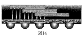
図14は、本発明の実施形態による半導体パッケージを示す。 FIG. 14 shows a semiconductor package according to an embodiment of the present invention.
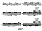
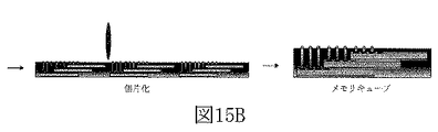
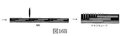
図15Aは、本発明の実施形態による半導体のパッケージ工法を示す。図15Aに示すように、ダミーウエハーが提供され、ダイが単位面積におけるダミーウエハー(次のステージにおいて各個の単位に分離される)に結着される。 FIG. 15A illustrates a semiconductor packaging method according to an embodiment of the present invention. As shown in FIG. 15A, a dummy wafer is provided and the die is bonded to a dummy wafer in a unit area (separated into individual units in the next stage).
また、図15Aを参照して、ピラーがダイに配置されるか、或いはダイボンディングの前に、ピラーを備えたダイが提供される。付加されたダイは、ダミーウエハーに結着されたダイにダイボンディングされ、付加されたピラーは、付加されたダイに配置される。図示されるように、三つのダイが積み重ねられるように互いに結着され、そのピラーがダイから垂直(図示された配向)に伸びる。三つ以上又は以下のダイがダイボンディングにより積み重ねられてもよい。ダイが積み重ねられた後、モールドがウエハーの周りに設けられ、封入材料がモールドに充填される。例えば、液体化合物がモールドに充填されて、積み重ねられたダイの周りに充填され、さらにダミーウエハーに流下する。 Referring also to FIG. 15A, a pillar with a pillar is provided before the pillar is placed on the die or prior to die bonding. The added die is die-bonded to the die bonded to the dummy wafer, and the added pillar is disposed on the added die. As shown, three dies are bonded together so that they are stacked, and their pillars extend vertically from the dies (the orientation shown). Three or more or less dies may be stacked by die bonding. After the dies are stacked, a mold is placed around the wafer and the encapsulant is filled into the mold. For example, a liquid compound is filled into a mold, filled around the stacked dies, and then flows down to a dummy wafer.
モールドが除去され、(硬化後の)封入材料が押し潰されて封入材料の表面にピラーを露出させる。 The mold is removed and the encapsulant (after curing) is crushed to expose the pillars on the surface of the encapsulant.
半田ペーストは、例えば、半田ペースト印刷工法により、露出したピラーに配置される。 The solder paste is disposed on the exposed pillar by, for example, a solder paste printing method.
図15Aに示すように、半田ペーストが配置された後、ダミーウエハーが押し潰される。一つ以上の実施形態において、ダミーウエハーは、研削しきれ、ダイスタックの最上のダイを露出させる。 As shown in FIG. 15A, after the solder paste is placed, the dummy wafer is crushed. In one or more embodiments, the dummy wafer can be ground to expose the top die of the die stack.
図15Bは、単位面積が単一化されて各個の半導体パッケージ単位に分離される次の製造ステージを示す。図15Bには、各個の半導体パッケージ単位は、例えば、「メモリキューブ」と標識されるが、説明される工法は、メモリに制限されていない。 FIG. 15B shows the next manufacturing stage in which the unit area is unified and separated into individual semiconductor package units. In FIG. 15B, each semiconductor package unit is labeled as, for example, “memory cube”, but the described method is not limited to memory.
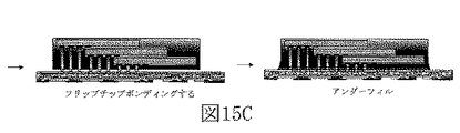
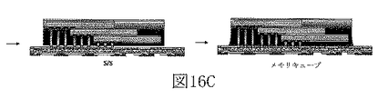
図15Cは、一つ以上の各々の半導体パッケージ単位がキャリア(例えば、RDLを備えた基板)と、半導体パッケージ単位とキャリアの間に適用されるアンダーフィルにフリップチップボンディングされる次の製造ステージを示す。 FIG. 15C shows the next manufacturing stage where one or more of each semiconductor package unit is flip chip bonded to a carrier (eg, a substrate with RDL) and an underfill applied between the semiconductor package unit and the carrier. Show.
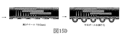
図15Dは、半導体パッケージ単位とキャリアの表面が封入材料により(例えば、モールド材料により)包まれ、半田ボールが適用される次の製造ステージを示す。続いて、可能であれば、キャリアと封入材料は、各個の装置、例えば、図14に示すような半導体パッケージに分離される。 FIG. 15D shows the next manufacturing stage where the semiconductor package unit and the surface of the carrier are encased in an encapsulating material (eg, in a mold material) and solder balls are applied. Subsequently, if possible, the carrier and encapsulating material are separated into individual devices, for example, semiconductor packages as shown in FIG.
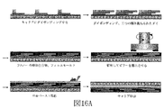
図16Aは、本発明の実施形態による半導体のパッケージ工法を示す。図16Aに示すように、ダミーキャリアは提供され、ダイが単位面積におけるキャリア(次のステージにおいて各個の単位に分離される)に結着される。 FIG. 16A illustrates a semiconductor packaging method according to an embodiment of the present invention. As shown in FIG. 16A, a dummy carrier is provided and the die is bound to a carrier in unit area (separated into individual units in the next stage).
また、図16Aを参照して、ピラーがダイに配置されるか、或いはダイボンディングの前に、ピラーを備えたダイが提供される。付加されたダイは、キャリアに結着されたダイにダイボンディングされ、付加されたピラーは、付加されたダイに配置される。図示されるように、三つのダイが積み重ねられるように互いに結着され、そのピラーがダイから垂直(図示された配向)に伸びる。三つ以上又は以下のダイがダイボンディングにより積み重ねられてもよい。ダイが積み重ねられた後、モールドがウエハーの周りに設けられ、封入材料がモールドに充填される。例えば、液体化合物がモールドに充填されて、積み重ねられたダイの周りに充填され、さらにキャリアに流下する。 Referring also to FIG. 16A, a pillar with a pillar is provided before the pillar is placed on the die or prior to die bonding. The added die is die-bonded to the die bonded to the carrier, and the added pillar is arranged on the added die. As shown, three dies are bonded together so that they are stacked, and their pillars extend vertically from the dies (the orientation shown). Three or more or less dies may be stacked by die bonding. After the dies are stacked, a mold is placed around the wafer and the encapsulant is filled into the mold. For example, a liquid compound is filled into a mold, filled around the stacked dies, and then flows down to the carrier.
ダイが積み重ねられた後、モールドがウエハーの周りに設けられ、封入材料がモールドに充填される。例えば、液体化合物がモールドに充填されて、積み重ねられたダイの周りに充填され、さらにダミーウエハーに流下する。 After the dies are stacked, a mold is placed around the wafer and the encapsulant is filled into the mold. For example, a liquid compound is filled into a mold, filled around the stacked dies, and then flows down to a dummy wafer.
モールドが除去され、(硬化後の)封入材料が押し潰されて封入材料の表面にピラーを露出させる。 The mold is removed and the encapsulant (after curing) is crushed to expose the pillars on the surface of the encapsulant.
半田ペーストは、例えば、半田ペースト印刷工法により、露出したピラーに配置される。図16Aに図示されるように、半田ペーストが配置された後、キャリアが除去される。 The solder paste is disposed on the exposed pillar by, for example, a solder paste printing method. As shown in FIG. 16A, after the solder paste is placed, the carrier is removed.
図16Bは、単位面積が単一化されて各個の半導体パッケージ単位を分離する次の製造ステージを示す。図16Bには、各個の半導体パッケージ単位は、例えば、「メモリキューブ」と標識されるが、説明される工法は、メモリに制限されていない。 FIG. 16B shows the next manufacturing stage in which the unit area is unified and each semiconductor package unit is separated. In FIG. 16B, each semiconductor package unit is labeled as, for example, “memory cube”, but the method described is not limited to memory.
図16Cは、一つ以上の各々の半導体パッケージ単位がキャリア(例えば、RDLを備えた基板)と、半導体パッケージ単位とキャリアの間に付けられたアンダーフィルにフリップチップボンディングされる次の製造ステージを示す。 FIG. 16C illustrates the next manufacturing stage where one or more of each semiconductor package unit is flip chip bonded to a carrier (eg, a substrate with RDL) and an underfill attached between the semiconductor package unit and the carrier. Show.
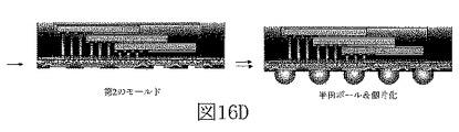
図16Dは、半導体パッケージ単位とキャリアの表面が封入材料により(例えば、モールド材料により)包まれ、半田ボールが適用される次の製造ステージを示す。続いて、可能であれば、キャリアと封入材料は、各個の装置、例えば、図14に示すような半導体パッケージに分離される。 FIG. 16D shows the next manufacturing stage where the semiconductor package unit and the surface of the carrier are encased in an encapsulating material (eg, in a mold material) and solder balls are applied. Subsequently, if possible, the carrier and encapsulating material are separated into individual devices, for example, semiconductor packages as shown in FIG.
ここで使用されたように、他に定義がない限り、「実質的に」、「実質的な」、「およそ」と「約」という文言は、説明のために使用され、小さな変形が考えられる。事件又は条件とともに使用される場合、それらの文言は、事件又は条件が適正に発生する例と、事件又は条件が近似値で発生する例を含む。例えば、数値とともに使用される場合、それらの文言は、例えば、±5%より小さいか等しい、±4%より小さいか等しい、±3%より小さいか等しい、±2%より小さいか等しい、±1%より小さいか等しい、±0.5%より小さいか等しい、±0.1%より小さいか等しい、或いは±0.05%より小さいか等しいなどの、その数値の±10%より小さいか等しい変化範囲を含む。「実質的に同一の平面にある」という文言は、同じ平面に、例えば、40μm以内、30μm以内、20μm以内、10μm以内、或いは1μm以内などのマイクロメートルのレベルで離れる二つの表面を言う。 As used herein, unless otherwise defined, the terms “substantially”, “substantial”, “approximately” and “about” are used for illustration and small variations are possible. . When used in conjunction with an incident or condition, these terms include examples where the incident or condition occurs properly and examples where the incident or condition occurs with an approximate value. For example, when used with numeric values, these terms are, for example, less than or equal to ± 5%, less than or equal to ± 4%, less than or equal to ± 3%, less than or equal to ± 2%, ± 1 It includes a range of change less than or equal to ± 10% of the numerical value, such as less than or equal to%, less than or equal to ± 0.5%, less than or equal to ± 0.1%, or less than or equal to ± 0.05%. The phrase “in substantially the same plane” refers to two surfaces that are separated in the same plane at a micrometer level, for example, within 40 μm, within 30 μm, within 20 μm, within 10 μm, or within 1 μm.
ここで使用されたように、単数の文言は、明確に説明されなければ、複数の指示対象の場合も含む。ある実施形態の説明には、他の部材「に」又は「の上に」設けられた部材は、前者の部材が直接(例えば、物理的接触がある)後者の部材にある例と、一つ以上のセパレータが前者の部材と後者の部材の間に位置する例を含む。 As used herein, a singular term includes the case of multiple indications unless specifically stated. In the description of an embodiment, a member provided “on” or “on” another member includes an example in which the former member is directly (eg, in physical contact) with the latter member. An example in which the above separator is positioned between the former member and the latter member is included.
本発明は、その詳しい実施形態によって説明され図示されたが、これらの説明と図示は、制限性のものではない。当業者であれば、添付クレームで定義される本発明の要旨から逸脱しない範囲で、各種の変更を行い、等価品と置き換えてもよいことが理解される。図式は、必ず一定の縮尺で描かれているとは限らない。製造プロセスと許容誤差のため、本発明における説明と実際な装置には区別があってもよい。詳しく図示されない本発明の他の実施形態もある。明細書と図式は、例示したものに限定されるわけではない。修正を行って特定の状態、材料、物質組成、方法、又はプロセスを本発明の目的、要旨と範囲に適合させることができる。このような修正は、ここに添付されたクレームの範囲に含まれる。ここに開示された方法は、特定の順で実行された特定の操作を参照して説明されたが、本発明の教示から逸脱しなければ、これらの操作を組み合わせ、細分し、或いは再び順番つけて等価の方法を形成してもよいことが理解される。したがって、ここで明確に指示しなければ、操作の順番と組み分けは、限定されるものではない。 Although the present invention has been described and illustrated by detailed embodiments thereof, these descriptions and illustrations are not limiting. It will be understood by those skilled in the art that various modifications may be made and replaced with equivalents without departing from the spirit of the invention as defined in the appended claims. Diagrams are not always drawn to scale. Because of the manufacturing process and tolerances, there may be a distinction between the description in the present invention and the actual apparatus. There are other embodiments of the present invention not shown in detail. The specification and schema are not limited to those illustrated. Modifications can be made to adapt a particular state, material, substance composition, method, or process to the purpose, spirit, and scope of the present invention. Such modifications are included within the scope of the claims appended hereto. Although the methods disclosed herein have been described with reference to particular operations performed in a particular order, these operations may be combined, subdivided, or reordered without departing from the teachings of the present invention. It is understood that equivalent methods may be formed. Therefore, unless specifically instructed here, the order and grouping of operations are not limited.
Claims (20)
第1の部分と第2の部分を含み、前記基板の前記第1の表面の上に配置されるパッドと、
前記第1の表面の上に配置され、前記パッドの前記第1の部分を被覆し、上面を有する第1の隔離層と、
前記パッドの前記第2の部分の上に配置され、上面を有する相互接続層と、
前記第1の隔離層の前記上面の上と前記相互接続層の前記上面の上に配置される導電性ポストと、を備え、
前記第1の隔離層の前記上面と前記相互接続層の前記上面が、実質的に同一の平面にある、半導体パッケージ。 A substrate having a first surface and a second surface opposite the first surface;
A pad comprising a first portion and a second portion, the pad being disposed on the first surface of the substrate;
A first isolation layer disposed on the first surface, covering the first portion of the pad and having an upper surface;
An interconnect layer disposed on the second portion of the pad and having an upper surface;
A conductive post disposed on the top surface of the first isolation layer and on the top surface of the interconnect layer;
The semiconductor package, wherein the top surface of the first isolation layer and the top surface of the interconnect layer are in substantially the same plane.
前記基板の前記第1の表面の上に配置され、第1の部分と、第2の部分と、第3の部分を含む導電性パッドと、
前記導電性パッドの前記第1の部分の上に配置される第1の隔離層と、
前記導電性パッドの前記第2の部分の上に配置され、上面を有する相互接続層と、
前記導電性パッドの前記第3の部分の上に配置される第2の隔離層と、
前記相互接続層の上と前記第1の隔離層の上に配置される導電性ポストと、を備え、
前記相互接続層の前記上面と前記第1の隔離層の上面が、実質的に同一の平面にある、半導体パッケージ。 A substrate having a first surface and a second surface opposite the first surface;
A conductive pad disposed on the first surface of the substrate and including a first portion, a second portion, and a third portion;
A first isolation layer disposed over the first portion of the conductive pad;
An interconnect layer disposed on the second portion of the conductive pad and having a top surface;
A second isolation layer disposed over the third portion of the conductive pad;
A conductive post disposed on the interconnect layer and on the first isolation layer; and
A semiconductor package, wherein the upper surface of the interconnect layer and the upper surface of the first isolation layer are in substantially the same plane.
前記導電性パッドの前記第1の部分を被覆するように、上面を有する第1の隔離層を形成する工程と、
上面を有する導電層を前記導電性パッドの前記第2の部分の上に配置する工程と、
前記第1の隔離層の前記上面の上と前記導電層の前記上面の上に導電性素子を配置する工程と、を含み、
前記第1の隔離層の前記上面と前記導電層の前記上面が、実質的に同一の平面にある、半導体パッケージを製造する方法。 A substrate having a first surface and a second surface facing the first surface; and a conductive pad including the first portion and the second portion and disposed on the first surface. Providing a process;
Forming a first isolation layer having an upper surface to cover the first portion of the conductive pad;
Disposing a conductive layer having a top surface on the second portion of the conductive pad;
Disposing a conductive element on the top surface of the first isolation layer and on the top surface of the conductive layer,
A method of manufacturing a semiconductor package, wherein the upper surface of the first isolation layer and the upper surface of the conductive layer are in substantially the same plane.
前記導電性素子の前記底面は、第1部と第2部を含み、前記第1部が、前記導電層の前記上面に接触し、前記第2部が、前記第1の隔離層の前記上面に接触する、請求項16に記載の前記方法。 The conductive element has a bottom surface;
The bottom surface of the conductive element includes a first part and a second part, the first part is in contact with the top surface of the conductive layer, and the second part is the top surface of the first isolation layer. 17. The method of claim 16, wherein the method contacts.
Applications Claiming Priority (6)
| Application Number | Priority Date | Filing Date | Title |
|---|---|---|---|
| US201662334861P | 2016-05-11 | 2016-05-11 | |
| US62/334,861 | 2016-05-11 | ||
| US201662352299P | 2016-06-20 | 2016-06-20 | |
| US62/352,299 | 2016-06-20 | ||
| US15/453,656 | 2017-03-08 | ||
| US15/453,656 US10049893B2 (en) | 2016-05-11 | 2017-03-08 | Semiconductor device with a conductive post |
Publications (3)
| Publication Number | Publication Date |
|---|---|
| JP2017204635A true JP2017204635A (en) | 2017-11-16 |
| JP2017204635A5 JP2017204635A5 (en) | 2018-10-18 |
| JP6557701B2 JP6557701B2 (en) | 2019-08-07 |
Family
ID=60294752
Family Applications (1)
| Application Number | Title | Priority Date | Filing Date |
|---|---|---|---|
| JP2017091536A Active JP6557701B2 (en) | 2016-05-11 | 2017-05-02 | Semiconductor device package and manufacturing method thereof |
Country Status (3)
| Country | Link |
|---|---|
| US (2) | US10049893B2 (en) |
| JP (1) | JP6557701B2 (en) |
| CN (2) | CN107424970B (en) |
Cited By (2)
| Publication number | Priority date | Publication date | Assignee | Title |
|---|---|---|---|---|
| CN112312254A (en) * | 2019-07-31 | 2021-02-02 | 日月光半导体制造股份有限公司 | Semiconductor device package and acoustic device having semiconductor device package |
| WO2025121102A1 (en) * | 2023-12-04 | 2025-06-12 | 株式会社村田製作所 | Circuit module |
Families Citing this family (13)
| Publication number | Priority date | Publication date | Assignee | Title |
|---|---|---|---|---|
| CN109075151B (en) | 2016-04-26 | 2023-06-27 | 亚德诺半导体国际无限责任公司 | Lead frame for mechanical mating, and electrical and thermal conduction of component package circuits |
| US10049893B2 (en) * | 2016-05-11 | 2018-08-14 | Advanced Semiconductor Engineering, Inc. | Semiconductor device with a conductive post |
| JP2019040924A (en) * | 2017-08-22 | 2019-03-14 | 新光電気工業株式会社 | Wiring board, manufacturing method thereof, and electronic device |
| US10741482B2 (en) * | 2017-12-29 | 2020-08-11 | Advanced Semiconductor Engineering, Inc. | Semiconductor device package |
| US10497635B2 (en) | 2018-03-27 | 2019-12-03 | Linear Technology Holding Llc | Stacked circuit package with molded base having laser drilled openings for upper package |
| US11735570B2 (en) * | 2018-04-04 | 2023-08-22 | Intel Corporation | Fan out packaging pop mechanical attach method |
| TWI672791B (en) * | 2018-05-07 | 2019-09-21 | 財團法人工業技術研究院 | Chip package structure and manufacturing method thereof |
| US11410977B2 (en) | 2018-11-13 | 2022-08-09 | Analog Devices International Unlimited Company | Electronic module for high power applications |
| US11235404B2 (en) * | 2020-03-21 | 2022-02-01 | International Business Machines Corporation | Personalized copper block for selective solder removal |
| EP4161222A4 (en) | 2020-05-26 | 2024-07-10 | LG Innotek Co., Ltd. | PACKAGING SUBSTRATE |
| US11844178B2 (en) | 2020-06-02 | 2023-12-12 | Analog Devices International Unlimited Company | Electronic component |
| US11476128B2 (en) | 2020-08-25 | 2022-10-18 | Advanced Semiconductor Engineering, Inc. | Semiconductor device package and method of manufacturing the same |
| CN117199053A (en) * | 2022-06-01 | 2023-12-08 | 长鑫存储技术有限公司 | Packaging structure and manufacturing method thereof, semiconductor device |
Citations (3)
| Publication number | Priority date | Publication date | Assignee | Title |
|---|---|---|---|---|
| US5912510A (en) * | 1996-05-29 | 1999-06-15 | Motorola, Inc. | Bonding structure for an electronic device |
| WO2014188760A1 (en) * | 2013-05-21 | 2014-11-27 | 株式会社村田製作所 | Module |
| WO2015198839A1 (en) * | 2014-06-27 | 2015-12-30 | ソニー株式会社 | Semiconductor device and manufacturing method therefor |
Family Cites Families (22)
| Publication number | Priority date | Publication date | Assignee | Title |
|---|---|---|---|---|
| JP3361881B2 (en) * | 1994-04-28 | 2003-01-07 | 株式会社東芝 | Semiconductor device and manufacturing method thereof |
| JP4564113B2 (en) * | 1998-11-30 | 2010-10-20 | 株式会社東芝 | Fine particle film forming method |
| TW464927B (en) * | 2000-08-29 | 2001-11-21 | Unipac Optoelectronics Corp | Metal bump with an insulating sidewall and method of fabricating thereof |
| US6683375B2 (en) * | 2001-06-15 | 2004-01-27 | Fairchild Semiconductor Corporation | Semiconductor die including conductive columns |
| US20030006062A1 (en) * | 2001-07-06 | 2003-01-09 | Stone William M. | Interconnect system and method of fabrication |
| JP2003069181A (en) * | 2001-08-28 | 2003-03-07 | Mitsubishi Electric Corp | Electronic apparatus and manufacturing method thereof |
| TWI245402B (en) * | 2002-01-07 | 2005-12-11 | Megic Corp | Rod soldering structure and manufacturing process thereof |
| US7749886B2 (en) * | 2006-12-20 | 2010-07-06 | Tessera, Inc. | Microelectronic assemblies having compliancy and methods therefor |
| DE102009010885B4 (en) * | 2009-02-27 | 2014-12-31 | Advanced Micro Devices, Inc. | Metallization system of a semiconductor device with metal columns with a smaller diameter at the bottom and manufacturing method thereof |
| US8383457B2 (en) * | 2010-09-03 | 2013-02-26 | Stats Chippac, Ltd. | Semiconductor device and method of forming interposer frame over semiconductor die to provide vertical interconnect |
| US8982107B2 (en) * | 2010-05-24 | 2015-03-17 | Sharp Kabushiki Kaisha | Scanning signal line drive circuit and display device provided with same |
| US8580607B2 (en) * | 2010-07-27 | 2013-11-12 | Tessera, Inc. | Microelectronic packages with nanoparticle joining |
| US9202715B2 (en) * | 2010-11-16 | 2015-12-01 | Stats Chippac Ltd. | Integrated circuit packaging system with connection structure and method of manufacture thereof |
| US8610285B2 (en) * | 2011-05-30 | 2013-12-17 | Taiwan Semiconductor Manufacturing Company, Ltd. | 3D IC packaging structures and methods with a metal pillar |
| US8535983B2 (en) * | 2011-06-02 | 2013-09-17 | Infineon Technologies Ag | Method of manufacturing a semiconductor device |
| US20130099371A1 (en) | 2011-10-21 | 2013-04-25 | Taiwan Semiconductor Manufacturing Company, Ltd. | Semiconductor package having solder jointed region with controlled ag content |
| TW201401456A (en) * | 2012-06-19 | 2014-01-01 | 矽品精密工業股份有限公司 | Substrate structure and package structure |
| TWI517318B (en) | 2013-06-14 | 2016-01-11 | 日月光半導體製造股份有限公司 | Substrate with metal column group and package structure with metal column group |
| TWI567902B (en) | 2013-06-14 | 2017-01-21 | 日月光半導體製造股份有限公司 | Substrate group with positioning group |
| US9478485B2 (en) * | 2013-06-28 | 2016-10-25 | STATS ChipPAC Pte. Ltd. | Semiconductor device and method of stacking semiconductor die on a fan-out WLCSP |
| US9653442B2 (en) * | 2014-01-17 | 2017-05-16 | Taiwan Semiconductor Manufacturing Company, Ltd. | Integrated circuit package and methods of forming same |
| US10049893B2 (en) * | 2016-05-11 | 2018-08-14 | Advanced Semiconductor Engineering, Inc. | Semiconductor device with a conductive post |
-
2017
- 2017-03-08 US US15/453,656 patent/US10049893B2/en active Active
- 2017-04-28 CN CN201710299264.5A patent/CN107424970B/en active Active
- 2017-04-28 CN CN201910779348.8A patent/CN110571158B/en active Active
- 2017-05-02 JP JP2017091536A patent/JP6557701B2/en active Active
-
2018
- 2018-08-13 US US16/102,527 patent/US10446411B2/en active Active
Patent Citations (3)
| Publication number | Priority date | Publication date | Assignee | Title |
|---|---|---|---|---|
| US5912510A (en) * | 1996-05-29 | 1999-06-15 | Motorola, Inc. | Bonding structure for an electronic device |
| WO2014188760A1 (en) * | 2013-05-21 | 2014-11-27 | 株式会社村田製作所 | Module |
| WO2015198839A1 (en) * | 2014-06-27 | 2015-12-30 | ソニー株式会社 | Semiconductor device and manufacturing method therefor |
Cited By (5)
| Publication number | Priority date | Publication date | Assignee | Title |
|---|---|---|---|---|
| CN112312254A (en) * | 2019-07-31 | 2021-02-02 | 日月光半导体制造股份有限公司 | Semiconductor device package and acoustic device having semiconductor device package |
| JP2021027308A (en) * | 2019-07-31 | 2021-02-22 | 日月光半導体製造股▲ふん▼有限公司 | Semiconductor device package and acoustic device including the same |
| JP7473322B2 (en) | 2019-07-31 | 2024-04-23 | 日月光半導体製造股▲ふん▼有限公司 | Semiconductor device package and acoustic device having same |
| US12401934B2 (en) | 2019-07-31 | 2025-08-26 | Advanced Semiconductor Engineering, Inc. | Semiconductor device package and acoustic device having the same |
| WO2025121102A1 (en) * | 2023-12-04 | 2025-06-12 | 株式会社村田製作所 | Circuit module |
Also Published As
| Publication number | Publication date |
|---|---|
| US10049893B2 (en) | 2018-08-14 |
| US20180350626A1 (en) | 2018-12-06 |
| US10446411B2 (en) | 2019-10-15 |
| CN110571158B (en) | 2021-12-21 |
| JP6557701B2 (en) | 2019-08-07 |
| CN107424970A (en) | 2017-12-01 |
| US20170330870A1 (en) | 2017-11-16 |
| CN107424970B (en) | 2019-09-20 |
| CN110571158A (en) | 2019-12-13 |
Similar Documents
| Publication | Publication Date | Title |
|---|---|---|
| JP6557701B2 (en) | Semiconductor device package and manufacturing method thereof | |
| US12191224B2 (en) | Semiconductor package and manufacturing method thereof | |
| JP6835798B2 (en) | Package structure and manufacturing method of package structure | |
| CN102214641B (en) | Wafer-level semiconductor package with stacking capability | |
| KR101892801B1 (en) | Integrated fan-out package and the methods of manufacturing | |
| KR100800478B1 (en) | Multilayer semiconductor package and manufacturing method thereof | |
| KR101429344B1 (en) | Semiconductor Package and Manufacturing Methode thereof | |
| US20180114781A1 (en) | Package structure and manufacturing method thereof | |
| TWI802726B (en) | Carrying substrate, electronic package having the carrying substrate, and methods for manufacturing the same | |
| CN106711118B (en) | Electronic package and its manufacturing method | |
| CN114725035B (en) | Fan-out double-sided packaging structure and preparation method of fan-out double-sided packaging structure | |
| CN104576593A (en) | Packaging structure and its manufacturing method | |
| CN104517922B (en) | Stacked package structure and its manufacturing method | |
| CN116230656A (en) | Electronic package and its manufacturing method | |
| TW202243166A (en) | Semiconductor package, package structure and manufacturing method thereof | |
| CN111883506B (en) | Electronic package, bearing substrate thereof and manufacturing method | |
| CN113410215A (en) | Semiconductor packaging structure and preparation method thereof | |
| TWI622143B (en) | Electronic package and its manufacturing method | |
| TW202306093A (en) | Semiconductor package | |
| KR101345035B1 (en) | Semiconductor package and fabricating method thereof | |
| TW201737415A (en) | Package substrate manufacturing method | |
| TWI612627B (en) | Electronic package and its manufacturing method | |
| CN107785329A (en) | Electronic packaging structure and its manufacturing method | |
| TW202335215A (en) | Semiconductor device and method for manufacturing semiconductor device |
Legal Events
| Date | Code | Title | Description |
|---|---|---|---|
| A521 | Request for written amendment filed |
Free format text: JAPANESE INTERMEDIATE CODE: A523 Effective date: 20180903 |
|
| A621 | Written request for application examination |
Free format text: JAPANESE INTERMEDIATE CODE: A621 Effective date: 20180903 |
|
| A871 | Explanation of circumstances concerning accelerated examination |
Free format text: JAPANESE INTERMEDIATE CODE: A871 Effective date: 20180903 |
|
| A975 | Report on accelerated examination |
Free format text: JAPANESE INTERMEDIATE CODE: A971005 Effective date: 20180926 |
|
| A131 | Notification of reasons for refusal |
Free format text: JAPANESE INTERMEDIATE CODE: A131 Effective date: 20181002 |
|
| A601 | Written request for extension of time |
Free format text: JAPANESE INTERMEDIATE CODE: A601 Effective date: 20181228 |
|
| A521 | Request for written amendment filed |
Free format text: JAPANESE INTERMEDIATE CODE: A523 Effective date: 20190228 |
|
| A131 | Notification of reasons for refusal |
Free format text: JAPANESE INTERMEDIATE CODE: A131 Effective date: 20190409 |
|
| A521 | Request for written amendment filed |
Free format text: JAPANESE INTERMEDIATE CODE: A523 Effective date: 20190612 |
|
| TRDD | Decision of grant or rejection written | ||
| A01 | Written decision to grant a patent or to grant a registration (utility model) |
Free format text: JAPANESE INTERMEDIATE CODE: A01 Effective date: 20190702 |
|
| A61 | First payment of annual fees (during grant procedure) |
Free format text: JAPANESE INTERMEDIATE CODE: A61 Effective date: 20190712 |
|
| R150 | Certificate of patent or registration of utility model |
Ref document number: 6557701 Country of ref document: JP Free format text: JAPANESE INTERMEDIATE CODE: R150 |
|
| R250 | Receipt of annual fees |
Free format text: JAPANESE INTERMEDIATE CODE: R250 |
|
| R250 | Receipt of annual fees |
Free format text: JAPANESE INTERMEDIATE CODE: R250 |
|
| R250 | Receipt of annual fees |
Free format text: JAPANESE INTERMEDIATE CODE: R250 |
|
| R250 | Receipt of annual fees |
Free format text: JAPANESE INTERMEDIATE CODE: R250 |