JP2017204576A - Power coil - Google Patents
Power coil Download PDFInfo
- Publication number
- JP2017204576A JP2017204576A JP2016095947A JP2016095947A JP2017204576A JP 2017204576 A JP2017204576 A JP 2017204576A JP 2016095947 A JP2016095947 A JP 2016095947A JP 2016095947 A JP2016095947 A JP 2016095947A JP 2017204576 A JP2017204576 A JP 2017204576A
- Authority
- JP
- Japan
- Prior art keywords
- coil
- power
- inner coil
- coils
- magnetic flux
- Prior art date
- Legal status (The legal status is an assumption and is not a legal conclusion. Google has not performed a legal analysis and makes no representation as to the accuracy of the status listed.)
- Granted
Links
Images


Classifications
-
- H—ELECTRICITY
- H02—GENERATION; CONVERSION OR DISTRIBUTION OF ELECTRIC POWER
- H02J—CIRCUIT ARRANGEMENTS OR SYSTEMS FOR SUPPLYING OR DISTRIBUTING ELECTRIC POWER; SYSTEMS FOR STORING ELECTRIC ENERGY
- H02J50/00—Circuit arrangements or systems for wireless supply or distribution of electric power
- H02J50/70—Circuit arrangements or systems for wireless supply or distribution of electric power involving the reduction of electric, magnetic or electromagnetic leakage fields
-
- B—PERFORMING OPERATIONS; TRANSPORTING
- B60—VEHICLES IN GENERAL
- B60L—PROPULSION OF ELECTRICALLY-PROPELLED VEHICLES; SUPPLYING ELECTRIC POWER FOR AUXILIARY EQUIPMENT OF ELECTRICALLY-PROPELLED VEHICLES; ELECTRODYNAMIC BRAKE SYSTEMS FOR VEHICLES IN GENERAL; MAGNETIC SUSPENSION OR LEVITATION FOR VEHICLES; MONITORING OPERATING VARIABLES OF ELECTRICALLY-PROPELLED VEHICLES; ELECTRIC SAFETY DEVICES FOR ELECTRICALLY-PROPELLED VEHICLES
- B60L50/00—Electric propulsion with power supplied within the vehicle
- B60L50/50—Electric propulsion with power supplied within the vehicle using propulsion power supplied by batteries or fuel cells
- B60L50/60—Electric propulsion with power supplied within the vehicle using propulsion power supplied by batteries or fuel cells using power supplied by batteries
-
- B—PERFORMING OPERATIONS; TRANSPORTING
- B60—VEHICLES IN GENERAL
- B60L—PROPULSION OF ELECTRICALLY-PROPELLED VEHICLES; SUPPLYING ELECTRIC POWER FOR AUXILIARY EQUIPMENT OF ELECTRICALLY-PROPELLED VEHICLES; ELECTRODYNAMIC BRAKE SYSTEMS FOR VEHICLES IN GENERAL; MAGNETIC SUSPENSION OR LEVITATION FOR VEHICLES; MONITORING OPERATING VARIABLES OF ELECTRICALLY-PROPELLED VEHICLES; ELECTRIC SAFETY DEVICES FOR ELECTRICALLY-PROPELLED VEHICLES
- B60L53/00—Methods of charging batteries, specially adapted for electric vehicles; Charging stations or on-board charging equipment therefor; Exchange of energy storage elements in electric vehicles
- B60L53/10—Methods of charging batteries, specially adapted for electric vehicles; Charging stations or on-board charging equipment therefor; Exchange of energy storage elements in electric vehicles characterised by the energy transfer between the charging station and the vehicle
- B60L53/12—Inductive energy transfer
- B60L53/126—Methods for pairing a vehicle and a charging station, e.g. establishing a one-to-one relation between a wireless power transmitter and a wireless power receiver
-
- H—ELECTRICITY
- H01—ELECTRIC ELEMENTS
- H01F—MAGNETS; INDUCTANCES; TRANSFORMERS; SELECTION OF MATERIALS FOR THEIR MAGNETIC PROPERTIES
- H01F27/00—Details of transformers or inductances, in general
- H01F27/006—Details of transformers or inductances, in general with special arrangement or spacing of turns of the winding(s), e.g. to produce desired self-resonance
-
- H—ELECTRICITY
- H01—ELECTRIC ELEMENTS
- H01F—MAGNETS; INDUCTANCES; TRANSFORMERS; SELECTION OF MATERIALS FOR THEIR MAGNETIC PROPERTIES
- H01F27/00—Details of transformers or inductances, in general
- H01F27/34—Special means for preventing or reducing unwanted electric or magnetic effects, e.g. no-load losses, reactive currents, harmonics, oscillations, leakage fields
- H01F27/346—Preventing or reducing leakage fields
-
- H—ELECTRICITY
- H01—ELECTRIC ELEMENTS
- H01F—MAGNETS; INDUCTANCES; TRANSFORMERS; SELECTION OF MATERIALS FOR THEIR MAGNETIC PROPERTIES
- H01F38/00—Adaptations of transformers or inductances for specific applications or functions
- H01F38/14—Inductive couplings
-
- H—ELECTRICITY
- H02—GENERATION; CONVERSION OR DISTRIBUTION OF ELECTRIC POWER
- H02J—CIRCUIT ARRANGEMENTS OR SYSTEMS FOR SUPPLYING OR DISTRIBUTING ELECTRIC POWER; SYSTEMS FOR STORING ELECTRIC ENERGY
- H02J50/00—Circuit arrangements or systems for wireless supply or distribution of electric power
- H02J50/10—Circuit arrangements or systems for wireless supply or distribution of electric power using inductive coupling
- H02J50/12—Circuit arrangements or systems for wireless supply or distribution of electric power using inductive coupling of the resonant type
-
- H—ELECTRICITY
- H02—GENERATION; CONVERSION OR DISTRIBUTION OF ELECTRIC POWER
- H02J—CIRCUIT ARRANGEMENTS OR SYSTEMS FOR SUPPLYING OR DISTRIBUTING ELECTRIC POWER; SYSTEMS FOR STORING ELECTRIC ENERGY
- H02J7/00—Circuit arrangements for charging or depolarising batteries or for supplying loads from batteries
- H02J7/0042—Circuit arrangements for charging or depolarising batteries or for supplying loads from batteries characterised by the mechanical construction
-
- B—PERFORMING OPERATIONS; TRANSPORTING
- B60—VEHICLES IN GENERAL
- B60L—PROPULSION OF ELECTRICALLY-PROPELLED VEHICLES; SUPPLYING ELECTRIC POWER FOR AUXILIARY EQUIPMENT OF ELECTRICALLY-PROPELLED VEHICLES; ELECTRODYNAMIC BRAKE SYSTEMS FOR VEHICLES IN GENERAL; MAGNETIC SUSPENSION OR LEVITATION FOR VEHICLES; MONITORING OPERATING VARIABLES OF ELECTRICALLY-PROPELLED VEHICLES; ELECTRIC SAFETY DEVICES FOR ELECTRICALLY-PROPELLED VEHICLES
- B60L2270/00—Problem solutions or means not otherwise provided for
- B60L2270/10—Emission reduction
- B60L2270/14—Emission reduction of noise
- B60L2270/147—Emission reduction of noise electro magnetic [EMI]
-
- B—PERFORMING OPERATIONS; TRANSPORTING
- B60—VEHICLES IN GENERAL
- B60M—POWER SUPPLY LINES, AND DEVICES ALONG RAILS, FOR ELECTRICALLY- PROPELLED VEHICLES
- B60M7/00—Power lines or rails specially adapted for electrically-propelled vehicles of special types, e.g. suspension tramway, ropeway, underground railway
-
- Y—GENERAL TAGGING OF NEW TECHNOLOGICAL DEVELOPMENTS; GENERAL TAGGING OF CROSS-SECTIONAL TECHNOLOGIES SPANNING OVER SEVERAL SECTIONS OF THE IPC; TECHNICAL SUBJECTS COVERED BY FORMER USPC CROSS-REFERENCE ART COLLECTIONS [XRACs] AND DIGESTS
- Y02—TECHNOLOGIES OR APPLICATIONS FOR MITIGATION OR ADAPTATION AGAINST CLIMATE CHANGE
- Y02T—CLIMATE CHANGE MITIGATION TECHNOLOGIES RELATED TO TRANSPORTATION
- Y02T10/00—Road transport of goods or passengers
- Y02T10/60—Other road transportation technologies with climate change mitigation effect
- Y02T10/70—Energy storage systems for electromobility, e.g. batteries
-
- Y—GENERAL TAGGING OF NEW TECHNOLOGICAL DEVELOPMENTS; GENERAL TAGGING OF CROSS-SECTIONAL TECHNOLOGIES SPANNING OVER SEVERAL SECTIONS OF THE IPC; TECHNICAL SUBJECTS COVERED BY FORMER USPC CROSS-REFERENCE ART COLLECTIONS [XRACs] AND DIGESTS
- Y02—TECHNOLOGIES OR APPLICATIONS FOR MITIGATION OR ADAPTATION AGAINST CLIMATE CHANGE
- Y02T—CLIMATE CHANGE MITIGATION TECHNOLOGIES RELATED TO TRANSPORTATION
- Y02T10/00—Road transport of goods or passengers
- Y02T10/60—Other road transportation technologies with climate change mitigation effect
- Y02T10/7072—Electromobility specific charging systems or methods for batteries, ultracapacitors, supercapacitors or double-layer capacitors
-
- Y—GENERAL TAGGING OF NEW TECHNOLOGICAL DEVELOPMENTS; GENERAL TAGGING OF CROSS-SECTIONAL TECHNOLOGIES SPANNING OVER SEVERAL SECTIONS OF THE IPC; TECHNICAL SUBJECTS COVERED BY FORMER USPC CROSS-REFERENCE ART COLLECTIONS [XRACs] AND DIGESTS
- Y02—TECHNOLOGIES OR APPLICATIONS FOR MITIGATION OR ADAPTATION AGAINST CLIMATE CHANGE
- Y02T—CLIMATE CHANGE MITIGATION TECHNOLOGIES RELATED TO TRANSPORTATION
- Y02T90/00—Enabling technologies or technologies with a potential or indirect contribution to GHG emissions mitigation
- Y02T90/10—Technologies relating to charging of electric vehicles
- Y02T90/14—Plug-in electric vehicles
Abstract
Description
本発明は、電力コイルに関するものである。 The present invention relates to a power coil.
特許文献1には、基準軸周りに導体線を周回させて構成された主コイルと、前記主コイルに対して予め設定された設定間隔だけ離間して配置されるとともに、前記主コイルと電気的に直列接続されて、前記主コイルと同じ交流電流が流れる補助コイルと、を備えたコイルアンテナが開示されている。
In
磁気的結合によって電力を送電する場合、送電コイルまたは受電コイルから磁界漏洩が発生する。磁界漏洩は、他の電子機器を干渉したり、人体へ影響を及ぼしたりするなどの恐れがある。 When power is transmitted by magnetic coupling, magnetic field leakage occurs from the power transmission coil or the power reception coil. Magnetic field leakage may interfere with other electronic devices or affect the human body.
なお、特許文献1では、主コイルに対し、補助コイルを基準軸方向に所定間隔だけ離間した構成により、磁界漏洩を抑制している。
In
そこで本発明は、磁界漏洩を抑制する技術を提供することを目的とする。 Then, an object of this invention is to provide the technique which suppresses magnetic field leakage.
本願は、上記課題の少なくとも一部を解決する手段を複数含んでいるが、その例を挙げるならば、以下の通りである。上記課題を解決すべく、本発明に係る電力コイルは、内側コイルと、前記内側コイルを囲うように形成され、外側において、前記内側コイルの外側の磁束と逆相の磁束を発生する、一端が第1の端子に接続され、他端が前記内側コイルの一端と接続された第1の外側コイルと、前記内側コイルを囲うように形成され、外側において、前記内側コイルの外側の磁束と逆相の磁束を発生する、一端が第2の端子に接続され、他端が前記内側コイルの他端と接続された第2の外側コイルと、を有することを特徴とする。 The present application includes a plurality of means for solving at least a part of the above-described problems. Examples of the means are as follows. In order to solve the above-mentioned problem, an electric power coil according to the present invention is formed so as to surround an inner coil and the inner coil, and generates an outer phase magnetic flux opposite to the outer magnetic flux of the inner coil. A first outer coil connected to the first terminal and having the other end connected to one end of the inner coil, and formed to surround the inner coil, and on the outer side, opposite to the magnetic flux outside the inner coil And a second outer coil having one end connected to the second terminal and the other end connected to the other end of the inner coil.
本発明によれば、磁界漏洩を抑制することができる。上記した以外の課題、構成、および効果は、以下の実施形態の説明により明らかにされる。 According to the present invention, magnetic field leakage can be suppressed. Problems, configurations, and effects other than those described above will be clarified by the following description of embodiments.
以下、本発明の実施の形態を、図面を参照して説明する。 Hereinafter, embodiments of the present invention will be described with reference to the drawings.
携帯端末などの携帯機器では、小型化、薄型化が進んだ反面、充電時のコネクタ接続が煩わしい状況にあり、無線給電による充電の要求が高まっている。また、電気自動車においては、有線による充電の場合、例えば、雨天時にコネクタに水が浸入し、接点が劣化する恐れがあることから、無線給電による充電が望ましい。また、介護向けの階段昇降機や移動式リフトなどにおいては、有線による充電の場合、例えば、被介護者がコネクタを機器に接続して充電することは困難であることから、無線給電による充電が望ましい。 While portable devices such as portable terminals have been reduced in size and thickness, connector connection at the time of charging is troublesome, and the demand for charging by wireless power feeding is increasing. Further, in the case of charging by electric wire in an electric vehicle, for example, charging may be performed by wireless power feeding because water may enter the connector in the rain and the contact may be deteriorated. Further, in the case of a stair lift or a mobile lift for nursing care, in the case of charging by wire, for example, it is difficult for a cared person to connect the connector to the device for charging, so charging by wireless power feeding is desirable. .
無線給電には、マイクロ波などの電波を用いるものや磁気的結合(電磁誘導)を用いるものが検討されている。マイクロ波は、伝送距離に優れるものの伝送効率が悪く実用化にはほとんど至っていない。これに対し、磁気的結合による無線給電は、伝送距離が数cmから10数cm程度であるが、送受電に用いるコイルの伝送効率は90%程度の高い効率が得られる。このようなことから、無線給電には、磁気的結合による伝送が主流になると考えられる。 For wireless power feeding, those using radio waves such as microwaves and those using magnetic coupling (electromagnetic induction) are being studied. Although microwaves are excellent in transmission distance, transmission efficiency is poor and practical use has hardly been achieved. On the other hand, in the wireless power feeding by magnetic coupling, the transmission distance is about several centimeters to several tens of centimeters, but the transmission efficiency of the coil used for power transmission / reception is as high as about 90%. For this reason, it is considered that transmission by magnetic coupling becomes the mainstream for wireless power feeding.
磁気的結合に用いられる送電周波数としては、100kHz帯、400kHz帯、6.78MHz帯、および13.56MHz帯などが考えられる。磁気的結合による無線給電は、伝送距離が比較的短いものの、送電コイルまたは受電コイルから磁界漏洩が発生する。他の電子機器や人体への影響を考慮すると、この磁界漏洩を極力低く抑える必要がある。 As a power transmission frequency used for magnetic coupling, a 100 kHz band, a 400 kHz band, a 6.78 MHz band, a 13.56 MHz band, and the like are conceivable. Although the wireless power feeding by magnetic coupling has a relatively short transmission distance, magnetic field leakage occurs from the power transmission coil or the power reception coil. Considering the influence on other electronic devices and the human body, it is necessary to suppress this magnetic field leakage as low as possible.
[第1の実施の形態]
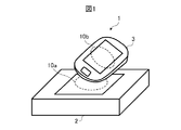
図1は、第1の実施の形態に係る無線給電システム1の例を示した図である。図1に示すように、無線給電システム1は、充電器2と、携帯端末3とを有している。
[First Embodiment]
FIG. 1 is a diagram illustrating an example of a wireless
充電器2の上部には、電力が充電される携帯端末3が置かれる。充電器2は、携帯端末3に電力を送電する電力コイル10aを内蔵している。
A
携帯端末3は、スマートフォンやタブレット端末、携帯電話などである。携帯端末3は、充電器2から電力を受電するための電力コイル10bを内蔵している。
The
電力コイル10a,10bは、同様の形状および構成を有している。そこで、以下では、電力コイル10a,10bを区別する必要がない場合には、まとめて電力コイル10と記載する。なお、後述するが、電力コイル10a,10bは、同様の形状および構成を有していない場合もある。
The
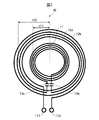
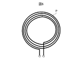
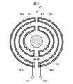
図2は、電力コイル10の構成例を示した図である。図2に示すように、電力コイル10は、端子T11,T12と、内側コイル11と、外側コイル12a,12bと、容量素子13a,13bとを有している。内側コイル11および外側コイル12a,12bは、同一(略同一を含む、以下同じ)平面上に形成されている。なお、図2では、内側コイル11および外側コイル12a,12bのそれぞれは、線と線の間に隙間があるように巻かれているが、実際は密に巻かれている。以下で説明するコイルも同様である。
FIG. 2 is a diagram illustrating a configuration example of the
外側コイル12a,12bは、それぞれ同じ(ほぼ同じを含む、以下同じ)形状を有し、同じ位置に配置されている。外側コイル12a,12bは、円形状を有し、その半径は、「r12」である。
The
内側コイル11は、円形状を有し、その半径は、外側コイル12a,12bの半径「r12」より小さく「r11」(r11<r12)である。内側コイル11は、外側コイル12a,12bのループ内に形成されている。
The
内側コイル11は、外側コイル12a,12bの間に、容量素子13a,13bを介して接続されている。容量素子13a,13bの合成の容量は、内側コイル11と外側コイル12a,12bとの合成の自己インダクタンスと、送電周波数で共振する値である。
The
外側コイル12aは、内側コイル11を囲うように形成されている。外側コイル12aは、その外側において、内側コイル11の外側の磁束と逆相の磁束を発生するように形成されている。
The
例えば、外側コイル12aは、内側コイル11を流れる電流とは逆向きの電流が流れるように形成される。より具体的には、内側コイル11に時計回りの電流が流れるとする。この場合、外側コイル12aは、反時計回りの電流が流れるように形成される。
For example, the
外側コイル12bは、内側コイル11を囲うように形成されている。外側コイル12bは、その外側において、内側コイル11の外側の磁束と逆相の磁束を発生するように形成されている。
The
例えば、外側コイル12bは、内側コイル11を流れる電流とは逆向きの電流が流れるように形成される。より具体的には、内側コイル11に時計回りの電流が流れるとする。この場合、外側コイル12bは、反時計回りの電流が流れるように形成される。
For example, the
外側コイル12aは、一端が端子T11に接続され、他端が容量素子13aに接続されている。外側コイル12bは、一端が端子T12に接続され、他端が容量素子13bに接続されている。端子T11,T12には、内側コイル11および外側コイル12a,12bから磁界を発生するための電流が入力される。
The
電力コイル10は、端子T11と接続されている外側コイル12aの一端と、端子T12と接続されている外側コイル12bの一端とから見て、対称(線対称)となるように形成されている。
The
図3は、電力コイル10の等価回路を示した図である。図3には、図2に示した端子T11,T12が示してある。
FIG. 3 is a diagram showing an equivalent circuit of the
図3のインダクタL11は、図2の外側コイル12aに対応している。図3の容量素子C11は、図2の容量素子13bに対応している。図3のインダクタL12は、図2の内側コイル11に対応している。図3の容量素子C12は、図2の容量素子13aに対応している。図3のインダクタL13は、図2の外側コイル12bに対応している。
The inductor L11 in FIG. 3 corresponds to the
図3に示すように、電力コイル10の等価回路も、端子T11と接続されている外側コイル12aの一端と、端子T12と接続されている外側コイル12bの一端とから見て、対称(素子の配置が線対称)となるように形成される。
As shown in FIG. 3, the equivalent circuit of the
内側コイル11と外側コイル12a,12bの大きさの関係および巻き数の関係について説明する。
The relationship between the size of the
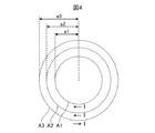
図4は、内側コイル11と外側コイル12a,12bの大きさの関係および巻き数の関係を説明する図である。
FIG. 4 is a diagram illustrating the relationship between the size of the
図4には、電流ループA1,A2,A3が示してある。電流ループA1,A2,A3の半径は、それぞれ「a1」,「a2」,「a3」とする。電流ループA1,A2には、時計回りに高周波電流Iが流れているとする。電流ループA3には、電流ループA1,A2とは逆向き(反時計回り)に高周波電流Iが流れているとする。 FIG. 4 shows current loops A1, A2 and A3. The radii of the current loops A1, A2, and A3 are “a1”, “a2”, and “a3”, respectively. It is assumed that the high-frequency current I flows clockwise through the current loops A1 and A2. It is assumed that the high-frequency current I flows in the current loop A3 in the opposite direction (counterclockwise) from the current loops A1 and A2.
電流ループA1から発生する磁界の強さは、電流ループA1の面積と、電流ループA1に流れる電流とに比例する。つまり、電流ループA1から発生する磁界の強さは、「a12・I」に比例する。 The strength of the magnetic field generated from the current loop A1 is proportional to the area of the current loop A1 and the current flowing through the current loop A1. That is, the strength of the magnetic field generated from the current loop A1 is proportional to “a1 2 · I”.
これにより、電流ループA1,A2,A3の遠方界での磁界漏洩を打ち消す条件は、電流の向きを考慮すると次の式(1)となる。 Thus, the condition for canceling the magnetic field leakage in the far field of the current loops A1, A2, and A3 is expressed by the following equation (1) in consideration of the direction of the current.
(a12+a22−a32)I=0 より (A1 2 + a2 2 −a3 2 ) From I = 0
a12+a22−a32=0 …(1) a1 2 + a2 2 −a3 2 = 0 (1)
内側と真中の電流ループA1,A2の半径が等しい場合の、電流ループA1,A2,A3の遠方界での磁界漏洩を打ち消す条件は、式(1)において、「a1=a2」と置くと、次の式(2)に示すようになる。 The condition for canceling the magnetic field leakage in the far field of the current loops A1, A2, and A3 when the radii of the inner and middle current loops A1 and A2 are equal is set as “a1 = a2” in Equation (1). The following equation (2) is obtained.
2a12=a32 より From 2a1 2 = a3 2
a3=21/2・a1 …(2) a3 = 2 1/2 · a1 (2)
以上から、半径「a1」の電流ループA1において、2倍の高周波電流Iを流すとともに、半径「21/2・a1」の電流ループA3において、高周波電流Iを逆方向に流せば、遠方界での磁界漏洩を打ち消すことが可能となる。 From the above, if the high frequency current I is doubled in the current loop A1 having the radius “a1” and the high frequency current I is supplied in the reverse direction in the current loop A3 having the radius “2 1/2 · a1”, the far field It is possible to cancel the magnetic field leakage at the point.
なお、磁界発生源からλ/(2π)より遠い場所を遠方界、近い場所を近傍界と呼ぶ。「λ」は、無線給電する電力の波長である。例えば、送電周波数が10MHzの場合、遠方界と近傍界との境界は、4.8mとなる。 A place farther than λ / (2π) from the magnetic field generation source is called a far field, and a place near the place is called a near field. “Λ” is a wavelength of power to be wirelessly fed. For example, when the power transmission frequency is 10 MHz, the boundary between the far field and the near field is 4.8 m.
上記条件を図2の電力コイル10に当てはめると、電力コイル10の遠方界での磁界漏洩を抑制することができる。例えば、図2の外側コイル12a,12bの半径「r12」を、内側コイル11の半径「r11」の21/2倍(略21/2倍を含む、以下同じ)にする。また、内側コイル11に流れる電流が、外側コイル12a,12bに流れる電流の2倍となるようにコイルを巻く。例えば、内側コイル11の巻き数を、外側コイル12aの巻き数と、外側コイル12bの巻き数とを加えた巻き数の2倍(略2倍を含む、以下同じ)となるようにする。これにより、電力コイル10の遠方界での磁界漏洩は、抑制される。
When the above conditions are applied to the
無線給電の際の磁界漏洩による影響が実際に重要視されるのは、他の電子機器などが、電力コイル10から数10cm〜数m程度の比較的近距離に置かれた場合である。そのため、近傍界での磁界漏洩の抑制も重要となってくる。
The effect of magnetic field leakage during wireless power feeding is actually regarded as important when other electronic devices are placed at a relatively short distance of several tens of centimeters to several meters from the
近傍界では、コイルからの距離が近くなることから、コイル形状なども磁界漏洩に影響してくるものと考えられる。電力コイル10では、図2に示す構成とすることにより、近傍界の漏洩電力も抑制することができる。特に、電力コイル10は、端子T11,T12と接続されている外側コイル12a,12bの一端から見て、対称となるように形成されるため、近傍界での磁界漏洩の抑制効果が大きくなる。また、電力コイル10は、等価回路も対称となるため、近傍界での磁界漏洩の抑制効果が大きくなる。
In the near field, since the distance from the coil is close, it is considered that the coil shape or the like also affects the magnetic field leakage. In the
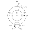
図5は、電力コイル10が発生する磁界を説明する図である。図5には、図2に示した電力コイル10が示してある。図5では、図2の電力コイル10を簡略化して示してある。図5において、図2と同じものには同じ符号が付してある。
FIG. 5 is a diagram illustrating a magnetic field generated by the
図5に示すように、端子T12から、電流Iが入力されたとする。この場合、内側コイル11の内側では、内側コイル11が発生する磁束と、外側コイル12a,12bが発生する磁束とによって、図5の磁束B11に示すように、紙面表側から紙面裏側に向かう磁束が発生する。
As shown in FIG. 5, it is assumed that the current I is input from the terminal T12. In this case, inside the
内側コイル11と外側コイル12a,12bとの間では、内側コイル11が発生する磁束と、外側コイル12a,12bが発生する磁束とによって、図5の磁束B12a,B12bに示すように、紙面裏側から紙面表側に向かう磁束が発生する。
Between the
外側コイル12a,12bの外側では、内側コイル11が発生する磁束と、外側コイル12a,12bが発生する磁束とによって、磁束は「0」(ほぼ0を含む、以下同じ)となる。すなわち、電力コイル10は、その近傍界においても磁界漏洩を抑制している。なお、電力コイル10からの距離に対する磁界漏洩の強さの測定結果については後述する(図15)。
Outside the
磁気的結合による無線給電では、給電側および受電側の電力コイルの巻き数が多いほど、電力コイル間の結合が大きくなり、電力の伝送効率が高くなる。しかし、電力コイルの巻き数を増やすと、線間での寄生容量が増加し、その寄生容量と、電力コイルの自己インダクタンスとで決まる自己共振周波数が低下する。このため、送電周波数に利用できる周波数範囲は、自己共振周波数の低下分だけ低くなる。また、自己共振周波数が低下することで、コイルのQ値(尖鋭度)が劣化する。 In wireless power feeding by magnetic coupling, the greater the number of turns of the power coil on the power feeding side and the power receiving side, the greater the coupling between the power coils and the higher the power transmission efficiency. However, when the number of turns of the power coil is increased, the parasitic capacitance between the lines increases, and the self-resonant frequency determined by the parasitic capacitance and the self-inductance of the power coil is lowered. For this reason, the frequency range that can be used for the power transmission frequency is lowered by the decrease in the self-resonant frequency. Moreover, Q value (sharpness) of a coil deteriorates because the self-resonance frequency falls.
しかし、電力コイル10は、内側コイル11と、外側コイル12a,12bとの間に容量素子13a,13bが接続される。容量素子13a,13bを備えることで、電力コイル10の寄生容量の原因となる巻き線間に溜まる電荷は、容量素子13a,13bに溜り、コイル線間に寄生容量が付きにくくなる。これにより、電力コイル10は、自己共振周波数の低下を抑制でき、内側コイル11および外側コイル12a,12bの巻き数を増やすことができる。つまり、電力コイル10は、コイル間の結合を大きくすることができ、電力の伝送効率を高くすることができる。
However, in the
また、磁気的結合による無線給電では、給電側および受電側の電力コイルの形状が同じであると、電力コイル間の結合が大きくなり、伝送効率が高くなる。しかし、給電側と受電側の電力コイルの形状が異なる場合もある。例えば、図1に示した充電器2には、様々な携帯端末3が置かれ、その携帯端末3は、様々な形状の電力コイルを有している場合がある。
In addition, in the wireless power feeding by magnetic coupling, when the shape of the power coil on the power feeding side and the power receiving side is the same, coupling between the power coils is increased, and transmission efficiency is increased. However, the shape of the power coil on the power feeding side and the power receiving side may be different. For example, various
図6は、別の電力コイルPの例を示した図である。図6に示す電力コイルPは、単に1方向に巻かれた円形状のコイルである。電力コイルPは、電力を受電する受電側のコイルの例を示している。 FIG. 6 is a diagram showing an example of another power coil P. The power coil P shown in FIG. 6 is simply a circular coil wound in one direction. The power coil P is an example of a coil on the power receiving side that receives power.
図7は、図6の電力コイルPの電力受電を説明する図である。図7には、図5に示した簡略化した電力コイル10が示してある。また、図7には、図6に示した電力コイルP(大きさが異なる電力コイルPa,Pb)が示してある。図7では、図6の電力コイルPa,Pbを簡略化して示してある。
FIG. 7 is a diagram illustrating power reception of the power coil P in FIG. 6. FIG. 7 shows the
図7に示す電力コイル10は、電力を送電する給電側(充電器2)の電力コイルとし、電力コイルPa,Pbは、電力を受電する受電側(携帯端末3)の電力コイルとする。以下では、電力コイルPa,Pbを区別する必要がない場合には、まとめて電力コイルPと記載する。
The
給電側の電力コイル10の内側コイル11は、受電側の電力コイルPより大きい方が望ましい。例えば、内側コイル11は、一点鎖線で示す受電側の電力コイルPaより小さいとする。この場合、一点鎖線の電力コイルPaには、磁束B11と、磁束B11と逆相の磁束B12a,12bとが入り込む。このため、一点鎖線で示す受電側の電力コイルPaでは、電力の伝送効率が低下する。
The
一方、内側コイル11は、点線で示す受電側の電力コイルPbより大きいとする。この場合、点線の電力コイルPbには、電力コイルPbが内側コイル11内に置かれる限り、1方向の磁束B11だけが入り込む。すなわち、点線の電力コイルPbには、磁束B11と逆相の磁束B12a,12bが入り込まない。このため、点線で示す電力コイルPbは、一点鎖線の電力コイルPaより、電力の伝送効率の低下が抑制される。
On the other hand, the
このように、給電側の電力コイルを電力コイル10とし、受電側の電力コイルを、電力コイル10とは異なる電力コイルPとすることもできる。その際、電力の伝送効率の低下を抑制するため、電力コイル10の内側コイル11は、電力コイルPより大きくする。
As described above, the power coil on the power feeding side can be the
もちろん、受電側の電力コイルが、給電側の電力コイル10と同じである場合に(つまり、受電側の電力コイルも電力コイル10である場合に)、電力の伝送効率は最もよくなる。例えば、図7に示す磁束B11は、受電側の電力コイル10の内側コイル11で受電され、磁束B12a,12bは、受電側の電力コイル10の内側コイル11と外側コイル12a,12bとの間のループ(空間)によって受電されるため、電力の伝送効率は最もよくなる。
Of course, when the power coil on the power receiving side is the same as the
以上説明したように、電力コイル10は、内側コイル11を囲うように形成され、外側において、内側コイル11の外側の磁束と逆相の磁束を発生する、一端が端子T11に接続され、他端が内側コイル11の一端と接続された外側コイル12aと、内側コイル11を囲うように形成され、外側において、内側コイル11の外側の磁束と逆相の磁束を発生する、一端が端子T12に接続され、他端が内側コイル11の他端と接続された外側コイル12bと、を有する。これにより、電力コイル10は、遠方界および近傍界での磁界漏洩を抑制することができる。
As described above, the
また、電力コイル10の内側コイル11および外側コイル12a,12bは、外側コイル12aの一端および外側コイル12bの一端から見て、対称となるように形成される。また、電力コイル10の等価回路も、外側コイル12aの一端および外側コイル12bの一端から見て、対称となるように形成される。これにより、電力コイル10は、近傍界での磁界漏洩を抑制することができる。
Further, the
また、電力コイル10の内側コイル11には、外側コイル12aを流れる電流と、外側コイル12bに流れる電流とを加算した電流に対し、略2倍の電流が流れる。また、外側コイル12aおよび外側コイル12bの半径は、内側コイル11の半径に対し、略21/2倍である。これにより、電力コイル10は、近傍界での磁界漏洩を抑制することができる。
In addition, a current approximately twice as large as the current obtained by adding the current flowing through the
また、電力コイル10は、内側コイル11と外側コイル12aとの間に接続される容量素子13aと、内側コイル11と外側コイル12bとの間に接続される容量素子13bと有する。これにより、電力コイル10は、自己共振周波数の低下を抑制することができる。
The
また、電力コイル10は、内側コイル11と外側コイル12a,12bとが同一平面上に形成されるため、小型化を図ることができる。
Moreover, since the
[第2の実施の形態]
第1の実施の形態では、2つの外側コイル12a,12bの間に、内側コイル11を接続した。第2の実施の形態では、2つの内側コイルの間に、外側コイルを接続する。
[Second Embodiment]
In the first embodiment, the
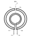
図8は、第2の実施の形態に係る電力コイル20の構成例を示した図である。図8に示すように、電力コイル20は、端子T21,T22と、内側コイル21a,21bと、外側コイル22と、容量素子23a,23bとを有している。内側コイル21a,21bおよび外側コイル22は、同一平面上に形成されている。電力コイル20は、電力を送電する給電側装置(例えば、図1の充電器2)または電力を受電する受電側装置(例えば、図1の携帯端末3)に適用される。
FIG. 8 is a diagram illustrating a configuration example of the
内側コイル21a,21bは、それぞれ同じ形状を有し、同じ位置に配置されている。内側コイル21a,21bは、円形状を有し、その半径は、「r21」である。
The
内側コイル21aは、一端が端子T21に接続され、他端が容量素子23bに接続されている。内側コイル21bは、一端が端子T22に接続され、他端が容量素子23aに接続されている。端子T21,T22には、内側コイル21a,21bおよび外側コイル22から磁界を発生するための電流が入力される。
The
外側コイル22は、円形状を有し、その半径は、内側コイル21a,21bの半径「r21」より大きく「r22」(r22>r21)である。内側コイル21a,21bは、外側コイル22のループ内に形成されている。
The
外側コイル22は、内側コイル21a,21bを囲うように形成されている。外側コイル22は、その外側において、内側コイル21a,21bの外側の磁束と逆相の磁束を発生するように形成されている。
The
例えば、外側コイル22は、内側コイル21a,21bを流れる電流とは逆向きの電流が流れるように形成される。より具体的には、内側コイル21a,21bに時計回りの電流が流れるとする。この場合、外側コイル22は、反時計回りの電流が流れるように形成される。
For example, the
外側コイル22は、内側コイル21a,21bの間に、容量素子23a,23bを介して接続されている。容量素子23a,23bの合成の容量は、内側コイル21a,21bと外側コイル22との合成の自己インダクタンスと、送電周波数で共振する値である。
The
電力コイル20は、端子T21と接続されている内側コイル21aの一端と、端子T22と接続されている内側コイル21bの一端とから見て、対称となるように形成されている。
The
図9は、電力コイル20の等価回路を示した図である。図9には、図8に示した端子T21,T22が示してある。
FIG. 9 is a diagram showing an equivalent circuit of the
図9のインダクタL21は、図8の内側コイル21aに対応している。図9の容量素子C21は、図8の容量素子23bに対応している。図9のインダクタL22は、図8の外側コイル22に対応している。図9の容量素子C22は、図8の容量素子23aに対応している。図9のインダクタL23は、図8の内側コイル21bに対応している。
The inductor L21 in FIG. 9 corresponds to the
図9に示すように、電力コイル20の等価回路も、端子T21と接続されている内側コイル21aの一端と、端子T22と接続されている内側コイル21bの一端とから見て、対称となるように形成される。
As shown in FIG. 9, the equivalent circuit of the
内側コイル21a,21bと外側コイル22の大きさの関係および巻き数の関係は、第1の実施の形態と同様である。例えば、図8に示した外側コイル22の半径「r22」を、内側コイル21a,21bの半径「r21」の21/2倍にする。また、内側コイル21a,21bに流れる電流が、外側コイル22に流れる電流の2倍となるようにコイルを巻く。例えば、内側コイル21aの巻き数と、内側コイル21bの巻き数とを加えた巻き数を、外側コイル22の巻き数の2倍となるようにする。これにより、電力コイル20の遠方界での磁界漏洩は、抑制される。
The relationship between the sizes of the
電力コイル20では、図8に示す構成とすることにより、近傍界の漏洩電力も抑制することができる。特に、電力コイル20は、端子T21と接続されている内側コイル21aの一端と、端子T22と接続されている内側コイル21bの一端とから見て、対称となるように形成されるため、近傍界での磁界漏洩の抑制効果が大きくなる。また、電力コイル20は、等価回路も対称となるため、近傍界での磁界漏洩の抑制効果が大きくなる。
In the
図10は、電力コイル20が発生する磁界を説明する図である。図10には、図8に示した電力コイル20が示してある。図10では、図8の電力コイル20を簡略化して示してある。図10において、図8と同じものには同じ符号が付してある。
FIG. 10 is a diagram illustrating a magnetic field generated by the
図10に示すように、端子T22から、電流Iが入力されたとする。この場合、内側コイル21a,21bの内側では、内側コイル21a,21bが発生する磁束と、外側コイル22が発生する磁束とによって、図10の磁束B21に示すように、紙面裏側から紙面表側に向かう磁束が発生する。
As shown in FIG. 10, it is assumed that the current I is input from the terminal T22. In this case, on the inner side of the
内側コイル21a,21bと外側コイル22との間では、内側コイル21a,21bが発生する磁束と、外側コイル22が発生する磁束とによって、図10の磁束B22a,B22bに示すように、紙面表側から紙面裏側に向かう磁束が発生する。
Between the
外側コイル22の外側では、内側コイル21a,21bが発生する磁束と、外側コイル22が発生する磁束とによって、磁束は「0」となる。すなわち、電力コイル20は、その近傍界においても磁界漏洩を抑制している。
Outside the
給電側の電力コイルと受電側の電力コイルとの巻き数による電力の伝送効率は、第1の実施の形態と同様であり、その説明を省略する。また、給電側の電力コイルと受電側の電力コイルとの形状による電力の伝送効率は、第1の実施の形態と同様であり、その説明を省略する。 The power transmission efficiency by the number of turns between the power supply-side power coil and the power-receiving-side power coil is the same as in the first embodiment, and the description thereof is omitted. The power transmission efficiency by the shapes of the power supply-side power coil and the power-receiving-side power coil is the same as that in the first embodiment, and a description thereof is omitted.
以上説明したように、電力コイル20は、内側コイル21a,21bを囲うように形成され、外側において、内側コイル21a,21bの外側の磁束と逆相の磁束を発生する、一端が内側コイル21aと接続され、他端が内側コイル21bと接続された外側コイル22を有する。これにより、電力コイル20は、遠方界および近傍界での磁界漏洩を抑制することができる。
As described above, the
また、電力コイル20の内側コイル21a,21bおよび外側コイル22は、内側コイル21aの一端および内側コイル21bの一端から見て、対称となるように形成される。また、電力コイル20の等価回路も、内側コイル21aの一端および内側コイル21bの一端から見て、対称となるように形成される。これにより、電力コイル20は、近傍界での磁界漏洩を抑制することができる。
Further, the
また、電力コイル20の内側コイル21a,21bには、外側コイル22を流れる電流に対し、略2倍の電流が流れる。また、外側コイル22の半径は、内側コイル21a,21bの半径に対し、略21/2倍である。これにより、電力コイル20は、近傍界での磁界漏洩を抑制することができる。
In addition, a current approximately twice as large as the current flowing through the
また、電力コイル20は、内側コイル21aと外側コイル22との間に接続される容量素子23bと、内側コイル21bと外側コイル22との間に接続される容量素子23aと有する。これにより、電力コイル20は、自己共振周波数の低下を抑制することができる。
The
また、電力コイル20は、内側コイル21a,21bと外側コイル22とが同一平面上に形成されるため、小型化を図ることができる。
Moreover, since the
[第3の実施の形態]
第1の実施の形態では、内側コイル11を囲う2つの外側コイル12a,12bは、同じ形状を有し、同じ位置に配置された。第3の実施の形態では、内側コイルを囲う2つの外側コイルを、異なる位置に配置する。
[Third Embodiment]
In the first embodiment, the two
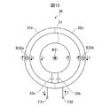
図11は、第3の実施の形態に係る電力コイル30の構成例を示した図である。図11に示すように、電力コイル30は、端子T31,T32と、内側コイル31と、外側コイル32a,32bと、容量素子33a,33bとを有している。内側コイル31および外側コイル32a,32bは、同一平面上に形成されている。電力コイル30は、電力を送電する給電側装置(例えば、図1の充電器2)または電力を受電する受電側装置(例えば、図1の携帯端末3)に適用される。
FIG. 11 is a diagram illustrating a configuration example of the
外側コイル32a,32bは、それぞれ同じ形状を有し、異なる位置に配置されている。外側コイル32a,32bは、円形状の内側コイル31の形状に沿った、三日月状の形状を有しているとともに、2つで円形状となる形状を有している。外側コイル32aは、内側コイル31の半分(略半分を含む、以下同じ)を囲い、外側コイル32bは、内側コイル31の残りの半分を囲っている。
The
内側コイル31は、外側コイル32a,32bの間に、容量素子33a,33bを介して接続されている。容量素子33a,33bの合成の容量は、内側コイル31と外側コイル32a,32bとの合成の自己インダクタンスと、送電周波数で共振する値である。
The
内側コイル31は、円形状を有している。内側コイル31は、外側コイル32a,32bのそれぞれのループの外側において、外側コイル32a,32bに囲まれるように配置される。
The
外側コイル32aは、内側コイル31の外側でループを形成し、そのループの外側において、内側コイル31の外側の磁束と逆相の磁束を発生するように形成されている。例えば、外側コイル32aは、内側コイル31を流れる電流とは逆向きの電流が流れるように形成される。より具体的には、内側コイル31に反時計回りの電流が流れるとする。この場合、外側コイル32aは、時計回りの電流が流れるように形成される。
The
外側コイル32bは、内側コイル31の外側でループを形成し、そのループの外側において、内側コイル31の外側の磁束と逆相の磁束を発生するように形成されている。例えば、外側コイル32bは、内側コイル31を流れる電流とは逆向きの電流が流れるように形成される。より具体的には、内側コイル31に反時計回りの電流が流れるとする。この場合、外側コイル32bは、時計回りの電流が流れるように形成される。
The
外側コイル32aは、一端が端子T31に接続され、他端が容量素子33aに接続されている。外側コイル32bは、一端が端子T32に接続され、他端が容量素子33bに接続されている。端子T31,T32には、内側コイル31および外側コイル32a,32bから磁界を発生するための電流が入力される。
The
電力コイル30は、端子T31と接続されている外側コイル32aの一端と、端子T32と接続されている外側コイル32bの一端とから見て、対称となるように形成されている。
The
図12は、電力コイル30の等価回路を示した図である。図12には、図11に示した端子T31,T32が示してある。
FIG. 12 is a diagram showing an equivalent circuit of the
図12のインダクタL31は、図11の外側コイル32aに対応している。図12の容量素子C31は、図11の容量素子33aに対応している。図12のインダクタL32は、図11の内側コイル31に対応している。図12の容量素子C32は、図11の容量素子33bに対応している。図12のインダクタL33は、図11の外側コイル32bに対応している。
The inductor L31 in FIG. 12 corresponds to the
図12に示すように、電力コイル30の等価回路も、端子T31と接続されている外側コイル32aの一端と、端子T32と接続されている外側コイル32bの一端とから見て、対称となるように形成される。
As shown in FIG. 12, the equivalent circuit of the
内側コイル31と外側コイル32a,32bの大きさの関係および巻き数の関係は、式(1)および式(2)より求まる。例えば、内側コイル31の面積は、外側コイル32a,32bのそれぞれの面積を加算した面積と同じにする。また、内側コイル31および外側コイル32a,32bは、それぞれに流れる電流が同じとなるようにコイルを巻く。例えば、内側コイル31および外側コイル32a,32bのそれぞれの巻き数は、同じにする。これにより、電力コイル30の遠方界での磁界漏洩は、抑制される。
The relationship between the size of the
電力コイル30では、図11に示す構成とすることにより、近傍界の漏洩電力も抑制することができる。特に、電力コイル30は、端子T31と接続されている外側コイル32aの一端と、端子T32と接続されている外側コイル32bの一端とから見て、対称となるように形成されるため、近傍界での磁界漏洩の抑制効果が大きくなる。また、電力コイル30は、等価回路も対称となるため、近傍界での磁界漏洩の抑制効果が大きくなる。
In the
また、電力コイル30では、次に説明するように、無線給電の際、給電側と受電側の電力コイル30の位置が多少ずれても、電力を効率よく伝送することができる。
In addition, as will be described below, the
図13は、電力コイル30が発生する磁界を説明する図である。図13には、図11に示した電力コイル30が示してある。図13では、図11の電力コイル30を簡略化して示してある。図13において、図11と同じものには同じ符号が付してある。
FIG. 13 is a diagram illustrating a magnetic field generated by the
図13に示すように、端子T32から、電流Iが入力されたとする。この場合、内側コイル31の内側では、内側コイル31が発生する磁束と、外側コイル32a,32bが発生する磁束とによって、図13の磁束B31に示すように、紙面裏側から紙面表側に向かう磁束が発生する。
As shown in FIG. 13, it is assumed that the current I is input from the terminal T32. In this case, inside the
内側コイル31と外側コイル32a,32bとの間では、内側コイル31が発生する磁束と、外側コイル32a,32bが発生する磁束とによって、磁束は「0」となる。すなわち、内側コイル31と外側コイル32a,32bとの間には、磁束の無い(ほぼ無いを含む、以下同じ)領域ができる。
Between the
外側コイル32a,32bのそれぞれの内側では、内側コイル31が発生する磁束と、外側コイル32a,32bが発生する磁束とによって、図13の磁束B32a,32bに示すように、紙面表側から紙面裏側に向かう磁束が発生する。
Inside each of the
外側コイル32a,32bの外側では、内側コイル31が発生する磁束と、外側コイル32a,32bが発生する磁束とによって、磁束は「0」となる。すなわち、電力コイル30は、その近傍界においても磁界漏洩を抑制している。
Outside the
図14は、電力の伝送効率を説明する図である。図14には、図13に示した電力コイル30が示してある。また、図14には、図6に示した電力コイルP(大きさが同じ電力コイルPa,Pb)が示してある。図14では、図6の電力コイルPa,Pbを簡略化して示してある。
FIG. 14 is a diagram illustrating power transmission efficiency. FIG. 14 shows the
図14に示す電力コイル30は、電力を送電する給電側の電力コイルとし、電力コイルPa,Pbは、電力を受電する受電側の電力コイルとする。以下では、電力コイルPa,Pbを区別する必要がない場合には、まとめて電力コイルPと記載する。電力コイルPは、内側コイル31より大きく、2つの外側コイル32a,32bが形成する円形状より、小さいとする。
The
図13で説明したように、内側コイル31と外側コイル32a,32bとの間には、磁束の無い領域ができる。そのため、点線の電力コイルPaに示すように、電力コイルPaの中心が、電力コイル30の中心と多少ずれても、電力コイルPaには、磁束B31が入り込み、磁束B31と逆相の磁束B32a,32bが入り込まない。これにより、電力コイル30では、受電側の電力コイルPaと多少の位置ずれが生じても、電力の伝送効率の低下を抑制できる。もちろん、一点鎖線の電力コイルPbに示すように、電力コイルPbの中心が、電力コイル30の中心と大きくずれると、電力コイルPbには、磁束B31と、磁束B31と逆相の磁束B32a,32bとが入り込み、電力の伝送効率は低下する。
As described with reference to FIG. 13, an area without magnetic flux is formed between the
上記では、受電側の電力コイルが、単に1方向に巻かれた円形状の電力コイルPである場合について説明したが、受電側の電力コイルが電力コイル30である場合も同様である。すなわち、給電側および受電側の電力コイルが電力コイル30である場合でも、多少の位置ずれに対し、電力の伝送効率の低下を抑制することができる。
In the above description, the case where the power coil on the power receiving side is simply the circular power coil P wound in one direction has been described, but the same applies to the case where the power coil on the power receiving side is the
図15は、電力コイルからの距離と磁界漏洩の強さの関係を示した図である。図15に示す横軸は、電力コイルの外側コイルからの距離を示し、縦軸は、磁界漏洩の強さを示している。なお、磁界漏洩の測定は、給電側の電力コイルと、受電側の電力コイルとの中心を合わせ、距離を10mm離した状態で行った。また、磁界漏洩の強さは、非共振のピックアップコイルにより受電した電力値により相対的に示したものである。 FIG. 15 is a diagram showing the relationship between the distance from the power coil and the strength of magnetic field leakage. The horizontal axis shown in FIG. 15 indicates the distance from the outer coil of the power coil, and the vertical axis indicates the strength of magnetic field leakage. The measurement of the magnetic field leakage was performed in a state where the centers of the power coil on the power feeding side and the power coil on the power receiving side were aligned and the distance was 10 mm apart. The strength of magnetic field leakage is relatively indicated by the power value received by the non-resonant pickup coil.
波形W1は、図6に示した電力コイルPの磁界漏洩の強さを示している。電力コイルPの半径は「2.5cm」、ターン数は「5」とした。 A waveform W1 indicates the strength of magnetic field leakage of the power coil P illustrated in FIG. The radius of the power coil P was “2.5 cm” and the number of turns was “5”.
波形W2は、図2に示した電力コイル10の磁界漏洩の強さを示している。内側コイル11は、半径を「2.5cm」、ターン数を「10」とした。また、外側コイル12a,12bは、半径を「3.5cm」、ターン数をそれぞれ「2.5」とした。
A waveform W2 indicates the strength of magnetic field leakage of the
波形W3は、図11に示した電力コイル30の磁界漏洩の強さを示している。内側コイル31は、半径を「2.5cm」、ターン数を「5」とした。また、外側コイル32a,32bは、外周の半径を「4.5cm」、内周の半径を「3.7cm」とし、ターン数をそれぞれ「5」とした。
A waveform W3 indicates the strength of magnetic field leakage of the
波形W2,W3に示すように、電力コイル10,30は、磁束打ち消し構造でない図6の電力コイルPに対し、磁界漏洩を抑圧していることが分かる。例えば、電力コイル10は、電力コイルPに対し、20dB前後の磁界漏洩の抑制効果が得られていることが分かる。
As shown by the waveforms W2 and W3, it can be seen that the power coils 10 and 30 suppress magnetic field leakage with respect to the power coil P of FIG. For example, it can be seen that the
なお、図8の電力コイル20は、図2の2つの外側コイル12a,12bの間に、内側コイル11を接続した電力コイル10に対し、2つの内側コイル21a,21bの間に、外側コイル22を接続したものである。従って、電力コイル20は、波形W2と同様の磁界漏洩の測定結果が得られる。例えば、電力コイル20の内側コイル21a,21bの半径を「2.5cm」、それぞれのターン数を「5」とし、外側コイル22の半径を「3.5cm」、ターン数を「5」とすれば、波形W2の磁界漏洩の強さが得られる。
Note that the
図16は、電力コイルの位置ずれと伝達特性の関係を示した図である。図15に示す横軸は、給電側の電力コイルの中心と、受電側の電力コイルの中心とのずれを示している。縦軸は、電力の伝達特性(S21)を示している。 FIG. 16 is a diagram showing the relationship between the displacement of the power coil and the transfer characteristics. The horizontal axis shown in FIG. 15 indicates the deviation between the center of the power coil on the power feeding side and the center of the power coil on the power receiving side. The vertical axis represents the power transfer characteristic (S21).
波形W11は、図6に示した電力コイルPの伝達特性を示している。波形W12は、図2に示した電力コイル10の伝達特性を示している。波形W13は、図11に示した電力コイル30の伝達特性を示している。電力コイルP,10,30の大きさおよび巻き数は、図15と同様である。
A waveform W11 shows the transfer characteristic of the power coil P shown in FIG. A waveform W12 shows the transfer characteristic of the
図2の電力コイル10では、波形W12に示すように「10mm」程度の位置ずれまで許容できると考えられる。図2の電力コイル10では、波形W13に示すように「17mm」程度の位置ずれまで許容できると考えられる。なお、図8の電力コイル20は、波形W12と同様の伝達特性の測定結果が得られる。
In the
以上説明したように、電力コイル30は、内側コイル31の外側でループを形成し、そのループの外側において、内側コイル31の外側の磁束と逆相の磁束を発生する、一端が端子T31と接続され、他端が内側コイル31の一端と接続された外側コイル32aと、内側コイル31の外側でループを形成し、そのループの外側において、内側コイル31の外側の磁束と逆相の磁束を発生する、一端が端子T32と接続され、他端が内側コイル31の他端と接続された外側コイル32bと、を有する。これにより、電力コイル30は、遠方界および近傍界での磁界漏洩を抑制することができる。また、給電側と受電側とにおいて、位置ずれが生じても、電力の伝送効率の低下を抑制することができる。
As described above, the
また、電力コイル30の内側コイル31および外側コイル32a,32bは、外側コイル32aの一端および外側コイル32bの一端から見て、対称となるように形成される。また、電力コイル30の等価回路も、外側コイル32aの一端および外側コイル32bの一端から見て、対称となるように形成される。これにより、電力コイル30は、近傍界での磁界漏洩を抑制することができる。
Further, the
また、電力コイル30の内側コイル31および外側コイル32a,32bのそれぞれには、略同じ電流が流れる。また、内側コイル31の面積は、外側コイル32aの面積と外側コイル32bの面積とを加算した面積と略同じである。これにより、電力コイル30は、近傍界での磁界漏洩を抑制することができる。
In addition, substantially the same current flows through each of the
また、電力コイル30は、内側コイル31と外側コイル32aとの間に接続される容量素子33aと、内側コイル31と外側コイル32bとの間に接続される容量素子33bと、を有する。これにより、電力コイル30は、自己共振周波数の低下を抑制することができる。
The
また、電力コイル30は、内側コイル31と外側コイル32a,32bとが同一平面上に形成されるため、小型化を図ることができる。
Moreover, since the
[第4の実施の形態]
第3の実施の形態では、内側コイル31を囲う2つの外側コイル32a,32bを、異なる位置に配置した。第4の実施の形態では、さらに2つの内側コイルを異なる位置に配置する。
[Fourth Embodiment]
In the third embodiment, the two
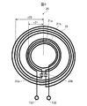
図17は、第4の実施の形態に係る電力コイル40の構成例を示した図である。図17に示すように、電力コイル40は、端子T41、T42と、内側コイル41a,41bと、外側コイル42a,42bと、容量素子43a,43bと、シャフト44とを有している。内側コイル41a,41bおよび外側コイル42a,42bは、同一平面上に形成されている。電力コイル40は、電力を送電する給電側装置(例えば、図1の充電器2)または電力を受電する受電側装置(例えば、図1の携帯端末3)に適用される。
FIG. 17 is a diagram illustrating a configuration example of the
図17に示すシャフト44は、その断面を示しており、紙面垂直方向に伸びている。シャフト44は、図17中において、時計回りまたは反時計回りに回転する。
The
内側コイル41a,41bは、それぞれ同じ形状を有し、異なる位置に配置されている。内側コイル41a,41bは、円形状のシャフト44の形状に沿った、三日月状の形状を有しているとともに、2つで円形状となる形状を有している。内側コイル41aは、ループ内にシャフト44を含まないよう(ループの外側で)シャフト44の半分を囲っている。内側コイル41bは、ループ内にシャフト44を含まないようシャフト44の残りの半分を囲っている。
The
外側コイル42a,42bは、それぞれ同じ形状を有し、異なる位置に配置されている。外側コイル42a,42bは、円形状の内側コイル41a,41bの形状に沿った、三日月状の形状を有しているとともに、2つで円形状となる形状を有している。外側コイル42aは、内側コイル41aを囲い、外側コイル42bは、内側コイル41bを囲っている。
The
外側コイル42aは、内側コイル41aの外側でループを形成し、そのループの外側において、内側コイル41aの外側の磁束と逆相の磁束を発生するように形成されている。例えば、外側コイル42aは、内側コイル41aを流れる電流とは逆向きの電流が流れるように形成される。より具体的には、内側コイル41aに反時計回りの電流が流れるとする。この場合、外側コイル42aは、時計回りの電流が流れるように形成される。
The
外側コイル42bは、内側コイル41bの外側でループを形成し、そのループの外側において、内側コイル41bの外側の磁束と逆相の磁束を発生するように形成されている。例えば、外側コイル42bは、内側コイル41bを流れる電流とは逆向きの電流が流れるように形成される。より具体的には、内側コイル41bに反時計回りの電流が流れるとする。この場合、外側コイル42bは、時計回りの電流が流れるように形成される。
The
内側コイル41aの一端は、内側コイル41bの一端と接続されている。内側コイル41aの他端は、容量素子43aを介して、外側コイル42aの他端と接続されている。外側コイル42aの一端は、端子T41と接続されている。内側コイル41bの他端は、容量素子43bを介して、外側コイル42bと接続されている。外側コイル42bの一端は、端子T42と接続されている。言い換えれば、2つの外側コイル42a,42bの間に、2つの内側コイル41a,41bが、容量素子43a,43bを介して接続されている。容量素子43a,43bの合成の容量は、内側コイル41a,41bと外側コイル42a,42bとの合成の自己インダクタンスと、送電周波数で共振する値である。端子T41,T42には、内側コイル41a,41bおよび外側コイル42a,42bから磁界を発生するための電流が入力される。
One end of the
電力コイル40は、端子T41と接続されている外側コイル42aの一端と、端子T42と接続されている外側コイル42bの一端とから見て、対称となるように形成されている。
The
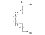
図18は、電力コイル40の等価回路を示した図である。図18には、図17に示した端子T41,T42が示してある。
FIG. 18 is a diagram showing an equivalent circuit of the
図18のインダクタL41は、図17の外側コイル42aに対応している。図18の容量素子C41は、図17の容量素子43aに対応している。図18のインダクタL42は、図17の内側コイル41aに対応している。図18のインダクタL43は、図17の内側コイル41bに対応している。図18の容量素子C42は、図17の容量素子43bに対応している。図18のインダクタL43は、図17の外側コイル42bに対応している。
The inductor L41 in FIG. 18 corresponds to the
図18に示すように、電力コイル40の等価回路も、端子T41と接続されている外側コイル42aの一端と、端子T42と接続されている外側コイル42bの一端とから見て、対称となるように形成される。
As shown in FIG. 18, the equivalent circuit of the
内側コイル41a,41bと外側コイル42a,42bの大きさの関係および巻き数の関係は、式(1)および式(2)より求まる。例えば、内側コイル41a,41bの加算した面積は、外側コイル42a,42bの加算した面積と同じにする。また、内側コイル41a,41bおよび外側コイル42a,42bは、それぞれに流れる電流が同じとなるようにコイルを巻く。例えば、内側コイル41a,41bおよび外側コイル42a,42bのそれぞれの巻き数は、同じにする。これにより、電力コイル40の遠方界での磁界漏洩は、抑制される。
The relationship between the sizes of the
電力コイル40では、図17に示す構成とすることにより、近傍界の漏洩電力も抑制することができる。特に、電力コイル40は、端子T41と接続されている外側コイル42aの一端と、端子T42と接続されている外側コイル42bの一端とから見て、対称となるように形成されるため、近傍界での磁界漏洩の抑制効果が大きくなる。また、電力コイル40は、等価回路も対称となるため、近傍界での磁界漏洩の抑制効果が大きくなる。
In the
図19は、電力コイル40が発生する磁界を説明する図である。図19には、図17に示した電力コイル40が示してある。図19では、図17の電力コイル40を簡略化して示してある。図19において、図17と同じものには同じ符号が付してある。
FIG. 19 is a diagram illustrating a magnetic field generated by the
図19に示すように、端子T42から、電流Iが入力されたとする。この場合、内側コイル41a,41bのループの外側であって、内側コイル41a,41bで囲まれる領域(シャフト44が存在している領域)では、内側コイル41a、41bが発生する磁束と、外側コイル42a,42bが発生する磁束とによって、磁束は「0」となる。すなわち、シャフト44が存在する領域では、磁束の無い領域ができる。これにより、シャフト44が金属である場合、シャフト44の表面に渦電流が流れることを抑制できる。
As shown in FIG. 19, it is assumed that the current I is input from the terminal T42. In this case, in the area outside the loop of the
内側コイル41a,41bのそれぞれの内側では、内側コイル41a,41bが発生する磁束と、外側コイル42a,42bが発生する磁束とによって、図19の磁束B41a,41bに示すように、紙面裏側から紙面表側に向かう磁束が発生する。
On the inner side of each of the
内側コイル41a,41bと外側コイル42a,42bとの間では、内側コイル41a,41bが発生する磁束と、外側コイル42a,42bが発生する磁束とによって、磁束は「0」となる。すなわち、内側コイル41a,41bと外側コイル42a,42bとの間には、磁束の無い領域ができる。
Between the
外側コイル42a,42bのそれぞれの内側では、内側コイル41a,41bが発生する磁束と、外側コイル42a,42bが発生する磁束とによって、図19の磁束B42a,42bに示すように、紙面表側から紙面裏側に向かう磁束が発生する。
On the inner side of each of the
外側コイル42a,42bの外側では、内側コイル41a,41bが発生する磁束と、外側コイル42a,42bが発生する磁束とによって、磁束は「0」となる。すなわち、電力コイル40は、その近傍界においても磁界漏洩を抑制している。
Outside the
以上説明したように、電力コイル40は、内側コイル41aを囲うように内側コイル41aの外側でループを形成し、そのループの外側において、内側コイル41aの外側の磁束と逆相の磁束を発生する、一端がT41端子と接続され、他端が内側コイル41aの他端と接続された外側コイル42aと、内側コイル41bを囲うように内側コイル41bの外側でループを形成し、そのループの外側において、内側コイル41bの外側の磁束と逆相の磁束を発生する、一端が端子T42と接続され、他端が内側コイル41bの他端と接続された外側コイル42bと、を有する。これにより、電力コイル40は、近傍界での磁界漏洩を抑制することができる。また、給電側と受電側において、位置ずれが生じても、電力の伝送効率の低下を抑制することができる。また、内側コイル41a,41b内に金属が存在しても、金属表面に渦電流が流れることによる、電力の伝送効率の低下を抑制することができる。
As described above, the
また、電力コイル40の内側コイル41a,41bおよび外側コイル42a,42bは、外側コイル42aの一端および外側コイル42bの一端から見て、対称となるように形成される。また、電力コイル40の等価回路も、外側コイル42aの一端および外側コイル42bの一端から見て、対称となるように形成される。これにより、電力コイル40は、近傍界での磁界漏洩を抑制することができる。
Further, the
また、電力コイル40の内側コイル41a,41bおよび外側コイル42a,42bのそれぞれには、略同じ電流が流れる。また、内側コイル41a,41の加算した面積は、外側コイル42a,42bの加算した面積と略同じである。これにより、電力コイル40は、近傍界での磁界漏洩を抑制することができる。
Further, substantially the same current flows through the
また、電力コイル40は、内側コイル41aと外側コイル42aとの間に接続される容量素子43aと、内側コイル41bと外側コイル42bとの間に接続される容量素子43bと、を有する。これにより、電力コイル40は、自己共振周波数の低下を抑制することができる。
The
また、電力コイル40は、内側コイル41a,41bと外側コイル42a,42bとが同一平面上に形成されるため、小型化を図ることができる。
Moreover, since the
なお、上記の各実施の形態で説明した電力コイル10〜40は円形状としたが、これに限られない。例えば、電力コイル10〜40は四角形状であってもよい。 Although the power coils 10 to 40 described in the above embodiments are circular, the present invention is not limited to this. For example, the power coils 10 to 40 may be rectangular.
[第5の実施の形態]
第5の実施の形態では、第1〜第4の実施の形態で示した電力コイルを用いた給電側装置および受電側装置について説明する。
[Fifth Embodiment]
In the fifth embodiment, a power feeding side device and a power receiving side device using the power coils shown in the first to fourth embodiments will be described.
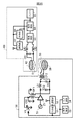
図20は、第5の実施の形態に係る給電側装置50および受電側装置60のブロック構成例を示した図である。図20に示すように、給電側装置50は、制御部51と、通信部52と、表示装置53と、入力装置54と、電力コイル55と、磁性体56と、電源V1と、容量素子C51,C52,C53と、コモンモードフィルタCF1,CF2と、発振器S1と、増幅器Z1と、インダクタL51と、を有している。受電側装置60は、電力コイル61と、磁性体62と、整流回路63と、電源回路64と、バッテリ65と、制御部66と、通信部67と、容量素子C61と,インダクタL61,L62とを有している。なお、図1に示した充電器2は、図20に示す給電側装置50を有し、携帯端末3は、受電側装置60を有している。
FIG. 20 is a diagram illustrating a block configuration example of the power
制御部51は、給電側装置50の全体を制御する。通信部52は、受電側装置60と無線通信を行う。制御部51は、通信部52を介して、受電側装置60が給電台(充電台)に置かれたか否かの検出を行う。また、制御部51は、給電台に置かれた受電側装置60が、充電対象機器であるかの認証を行う。また、制御部51は、電力の送電量を制御する。
The
表示装置53は、制御部51の制御に応じて、所定の情報を表示する。入力装置54は、ユーザの操作を受付け、受付けた操作情報を制御部51へ出力する。
The
電源V1は、容量素子C51によって高周波接地されている。電源V1は、コモンモードフィルタCF1を介して、電力を増幅器Z1に供給している。コモンモードフィルタCF1は、電源V1と増幅器Z1との間に接続され、電源ラインから進入する伝導ノイズ(コモンモードノイズ)を抑制する。 The power source V1 is high-frequency grounded by the capacitive element C51. The power source V1 supplies power to the amplifier Z1 through the common mode filter CF1. The common mode filter CF1 is connected between the power supply V1 and the amplifier Z1, and suppresses conduction noise (common mode noise) entering from the power supply line.
増幅器Z1には、発振器S1から出力される発振信号が入力される。増幅器Z1は、発振信号に応じて、スイッチング動作をし、送電信号(送電電力)を出力する。また、増幅器Z1は、制御部51の制御に応じて、送電電力の大きさ(増幅率)を変える。送電電力は、インダクタL51と容量素子C52,C53とによって形成されるローパスフィルタと、コモンモードフィルタCF2とを介して、電力コイル55へ出力される。
The oscillation signal output from the oscillator S1 is input to the amplifier Z1. The amplifier Z1 performs a switching operation according to the oscillation signal and outputs a power transmission signal (transmission power). In addition, the amplifier Z1 changes the magnitude (amplification factor) of the transmission power in accordance with the control of the
ローパスフィルタは、増幅器Z1と電力コイル55との間に接続され、送電電力に含まれる高調波ノイズを除去する。コモンモードフィルタCF2は、増幅器Z1と電力コイル55との間に接続され、送電電力に含まれる伝導ノイズを抑制し、伝導ノイズが電力コイル55から不要放射されるのを抑制する。
The low pass filter is connected between the amplifier Z1 and the
電力コイル55は、図2に示した電力コイル10、図8に示した電力コイル20、図11に示した電力コイル30、または図17に示した電力コイル40である。電力コイル55は、増幅器Z1から出力される送電電力を、磁気的結合により受電側装置60へ無線給電する。磁性体56は、給電側装置50の金属筐体などによる電力の伝送効率の低下を抑制する。また、磁性体56は、給電側装置50の金属筐体などの発熱を抑制する。
The
受電側装置60の電力コイル61は、図2に示した電力コイル10、図8に示した電力コイル20、図11に示した電力コイル30、または図17に示した電力コイル40である。電力コイル61は、給電側装置50から送電される電力を、磁気的結合によって受電する。磁性体62は、磁性体56と同様であり、電力の伝送効率の低下や、給電側装置50の金属筐体などの発熱等を抑制する。
The
なお、電力コイル61は、給電側装置50の電力コイル55と同じ型の電力コイルを用いるのがよい。また、電力コイル61には、図6に示した電力コイルPを用いてもよい。電力コイル61に、電力コイルPを用いる場合、電力コイル61とローパスフィルタとの間に共振用の容量素子を直列に接続する。そして、電力コイル61と容量素子とを、送電周波数で直列共振させる。
The
容量素子C61とインダクタL61,L62は、ローパスフィルタを形成している。ローパスフィルタは、電力コイル61によって受電された電力に含まれる高調波ノイズを抑制する。また、ローパスフィルタは、整流回路63から出力される高調波ノイズを抑制し、整流回路63から出力される高調波ノイズが、電力コイル61から再放射されるのを抑制する。
Capacitance element C61 and inductors L61 and L62 form a low-pass filter. The low pass filter suppresses harmonic noise included in the power received by the
整流回路63は、電力コイル61によって受電された電力を整流する(交流から直流に変換する)。電源回路64は、整流された電力をバッテリ65、制御部66、および通信部67へ出力する。
The rectifier circuit 63 rectifies the power received by the power coil 61 (converts from alternating current to direct current). The
バッテリ65は、整流回路63から出力される電力を充電する。制御部66は、受電側装置60の全体を制御している。制御部66は、電源回路64から出力される電力(電圧)が適切な電圧となるように、電源回路64を制御する。また、制御部66は、現在受電している電力量や満充電になったかなどの充電の状態を、通信部67を介して、給電側装置50へ送信する。通信部67は、給電側装置50と無線通信を行う。
The
図21は、給電側装置50の制御部51の動作例を示したフローチャートである。制御部51は、例えば、電源が投入されると、図21のフローチャートを実行する。
FIG. 21 is a flowchart illustrating an operation example of the
まず、制御部51は、増幅器Z1を制御し、電力コイル55から小電力の電力が送電されるようにする(ステップS1)。すなわち、制御部51は、受電側装置60が最低限動作する電力を送電する。
First, the
次に、制御部51は、通信部52を介して、受電側装置60と無線通信ができたか否か判定する(ステップS2)。すなわち、制御部51は、受電側装置60との無線通信によって、給電台に受電側装置60が置かれたか否か判定する。
Next, the
制御部51は、ステップS2にて、通信ができなかったと判定した場合(S2の「No」)ステップS1へ処理を移行する。
If it is determined in step S2 that communication has failed ("No" in S2), the
制御部51は、ステップS2にて、通信ができたと判定した場合(S2の「Yes」)、給電台に置かれた受電側装置60が適切な装置であるか認証処理を行う(ステップS3)。ここでは、制御部51は、受電側装置60を適切な装置であると認証し、処理をステップS4へ移行する。
If the
制御部51は、給電台に置かれた受電側装置60に対し、給電を行うか否か判定する(ステップS4)。例えば、制御部51は、通信部52を介して、受電側装置60から、満充電であるか否かの情報を受信し、給電を行うか否か判定する。
The
制御部51は、ステップS4にて、給電を行わないと判定した場合(S4の「No」)、表示装置53にアラートを表示する(ステップS5)。例えば、制御部51は、表示装置に、給電台に置かれた受電側装置60は満充電である旨を表示する。そして、制御部51は、受電側装置60への給電を終了し、当該フローチャートの処理を終了する。
When it is determined in step S4 that power feeding is not performed (“No” in S4), the
制御部51は、ステップS4にて、給電を行うと判定した場合(S4の「Yes」)、給電台に置かれた受電側装置60が、磁界漏洩を低減する電力コイルを搭載しているか否か判定する(ステップS6)。例えば、制御部51は、通信部52を介して、受電側装置60から、搭載している電力コイルの情報を受信し、その情報に基づいて、磁界漏洩を低減する電力コイルを搭載しているか否か判定する。または、制御部51は、通信部52を介して、受電側装置60から、搭載している電力コイルの情報を受信しなかった場合、受電側装置60磁界漏洩を低減する電力コイルを搭載していないと判定する。
If it is determined in step S4 that the power supply is to be performed (“Yes” in S4), the
なお、磁界漏洩を低減する電力コイルとは、図2に示した電力コイル10、図8に示した電力コイル20、図11に示した電力コイル30、または図17に示した電力コイル40である。磁界漏洩を低減しない電力コイルとは、例えば、図6に示した電力コイルPである。または、磁界漏洩を低減しない電力コイルとは、電力コイル55と形状が異なる電力コイルである。具体的には、電力コイル55が電力コイル10であって、電力コイル61が電力コイル20である場合である。
The power coil for reducing magnetic field leakage is the
制御部51は、ステップS6にて、給電台に置かれた受電側装置60が、磁界漏洩を低減する電力コイルを搭載していると判定した場合(S6の「Yes」)、通常の大きさの電力を送電する(ステップS7)。
When the
そして、制御部51は、受電側装置60の充電が終了したか否か判定する(ステップS8)。例えば、制御部51は、通信部52を介して、受電側装置60から、充電情報を受信し、受電側装置60の充電が終了したか否か判定する。
And the
制御部51は、ステップS8にて、受電側装置60の充電が終了していないと判定した場合(S8の「No」)、ステップS8の処理を繰り返す。一方、制御部51は、ステップS8にて、受電側装置60の充電が終了したと判定した場合(S8の「Yes」)、当該フローチャートの処理を終了する。
When it is determined in step S8 that charging of the power receiving
制御部51は、ステップS6にて、給電台に置かれた受電側装置60が、磁界漏洩を低減する電力コイルを搭載していないと判定した場合(S6の「No」)、磁界漏洩が大きくても、通常の電力送電を行うか否か、入力装置54を介してユーザから受付ける(ステップS9)。なお、制御部51は、ユーザから、通常の電力送電を行うか否かを受付ける際、磁界漏洩が大きくても、通常の電力送電を行うか否かを問う画面を、表示装置53に表示する。
When the
制御部51は、ユーザから、入力装置54を介して、通常の電力送電を行うと受付けた場合(S9の「Yes」)、処理をステップS7へ移行する。
If the
制御部51は、ユーザから、入力装置54を介して、通常の電力送電を行わないと受付けた場合(S9の「No」)、通常の電力より低い電力を受電側装置60へ送電する(ステップS10)。すなわち、制御部51は、送電電力を小さくし、磁界漏洩が小さくなるようにする。つまり、給電側装置50は、周囲の電子機器等に対する磁界漏洩の影響を小さくする。
When the
そして、制御部51は、受電側装置60の充電が終了したか否か判定する(ステップS11)。制御部51は、ステップS11にて、受電側装置60の充電が終了していないと判定した場合(S11の「No」)、ステップS11の処理を繰り返す。一方、制御部51は、ステップS11にて、受電側装置60の充電が終了したと判定した場合(S11の「Yes」)、当該フローチャートの処理を終了する。
And the
なお、ステップS9の処理は、省略してもよい。 Note that the process of step S9 may be omitted.
以上説明したように、給電側装置50は、増幅器Z1と、電源V1と増幅器Z1との間に接続されたコモンモードフィルタCF1と、増幅器Z1と電力コイル55との間に接続されたコモンモードフィルタCF2と、を有する。これにより、給電側装置50は、磁界漏洩を抑制することができる。また、給電側装置50は、送電電力に含まれる伝導ノイズを抑制し、伝導ノイズが電力コイル55から不要放射されるのを抑制することができる。
As described above, the power
受電側装置60は、電力コイル61によって受電された電力を整流する整流回路63と、電力コイル61と整流回路63との間に接続されたローパスフィルタと、を有する。これにより、受電側装置60は、磁界漏洩を抑制することができる。また、受電側装置60は、整流回路63で発生する受電電力の高調波成分が、電力コイル61より再放射されることを抑制することができる。
The power receiving
上記では、給電側装置50および受電側装置60の適用例として、充電器2および携帯端末3を例に挙げた。以下では、給電側装置50および受電側装置60のその他の適用例について説明する。
In the above, the
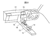
図22は、給電側装置50および受電側装置60の適用例を示した図のその1である。図22には、自動車の一部が示してある。自動車は、充電器71と、センターコンソール73と、スマートキー74と、ラジオ75と、カーナビゲーション76と、ダッシュボード77とを有している。また、図22には、携帯端末72が示してある。
FIG. 22 is a first diagram illustrating an application example of the power
充電器71は、図20に示した給電側装置50を有している。携帯端末72は、図20に示した受電側装置60を有している。携帯端末72は、例えば、スマートフォンやタブレット端末、携帯電話などである。携帯端末72は、受電側装置60が備えるバッテリ65によって動作する。携帯端末72のバッテリ65は、充電器71に置かれると充電される。
The
充電器71は、センターコンソール73に搭載されている。センターコンソール73は、携帯端末72の形状に沿った凹形状が形成され、そこに充電器71を搭載している。これにより、携帯端末72は、走行中であっても、充電器71からずれ落ちることなく、充電器71から充電されることができる。なお、充電器71は、電力コイルの中心部に磁石を実装し、携帯端末3を磁力で吸着するようにしてもよい。この場合、充電器71は、ダッシュボード77に設けられてもよい。
The
以上説明したように、給電側装置50および受電側装置60は、自動車に適用することができる。給電側装置50および受電側装置60は、磁界漏洩を抑制するので、スマートキー74、ラジオ75、およびカーナビゲーション76などの無線機器への干渉や誤動作、ノイズ混入などを抑制することができる。
As described above, the power
図23は、給電側装置50および受電側装置60の適用例を示した図のその2である。図22には、着地台81と、無人航空機82とが示してある。
FIG. 23 is a second diagram illustrating an application example of the power
着地台81は、図20に示した給電側装置50を有している。無人航空機82は、図20に示した受電側装置60を有している。無人航空機82は、無線によって、飛行が操作される。無人航空機82は、受電側装置60が備えるバッテリ65で飛行する。
The landing table 81 has the power
着地台81には、無人航空機82が着地する。無人航空機82が着地台81に着地すると、着地台81が備える電力コイル55と、無線航空機82が備える電力コイル61とが対向するようになっている。これにより、無人航空機82のバッテリ65は、着地台81に着地すると、充電されることができる。
An unmanned
以上説明したように、給電側装置50および受電側装置60は、着地台81および無人航空機82に適用することができる。給電側装置50および受電側装置60は、磁界漏洩を抑制するので、無人航空機82に搭載された通信回路やGPS(Global Positioning System)等への干渉や誤動作、ノイズ混入などを抑制することができる。
As described above, the power
図24は、給電側装置50および受電側装置60の適用例を示した図のその3である。図22には、充電器91と、自動車92とが示してある。
FIG. 24 is a third diagram illustrating an application example of the
充電器91は、図20に示した給電側装置50を有している。充電器91は、例えば、駐車場の地中等に設置されている。
The
自動車92は、図20に示した受電側装置60を有している。自動車92は、受電側装置60が備えるバッテリ65で走行する。また、自動車92の各電子装置は、バッテリ65で動作する。
The
自動車92は、例えば、駐車場等の所定の場所で停車すると、電力コイル61が、充電器91の電力コイル55と対向するようになっている。これにより、自動車92のバッテリ65は充電される。
For example, when the
以上説明したように、給電側装置50および受電側装置60は、充電器91および自動車92に適用することができる。給電側装置50および受電側装置60は、磁界漏洩を抑制するので、自動車92に搭載されているスマートキーや盗難防止装置、空気圧センサなどの電子機器への干渉や誤動作、ノイズ混入などを抑制することができる。
As described above, the power
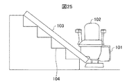
図25は、給電側装置50および受電側装置60の適用例を示した図のその4である。図25には、階段の歩行が困難な被介護者等向けの階段昇降機が示してある。図25には、充電器101と、椅子102と、レール103と、階段104とが示してある。
FIG. 25 is a fourth diagram illustrating an application example of the power
充電器101は、図20に示した給電側装置50を有している。充電器101は、例えば、レール103の端に位置する壁に設置されている。
The
椅子102は、図20に示した受電側装置60を有している。椅子102は、レール103に沿って移動できるように、レール103に連結されている。レール103は、階段104に沿うように、例えば、壁に取り付けられている。椅子102は、モータ等の駆動装置を備え、受電側装置60が備えるバッテリ65によって、レール103に沿って移動する。
The
椅子102は、レール103に沿って、充電器101の位置に来ると、電力コイル61が、充電器101の電力コイル55と対向するようになっている。これにより、椅子102のバッテリ65は充電される。
When the
以上説明したように、給電側装置50および受電側装置60は、充電器101および階段104を昇降する椅子102に適用することができる。給電側装置50および受電側装置60は、磁界漏洩を抑制するので、例えば、被介護者が装着した心臓ペースメーカや補聴器などの医療機器に対して、干渉の影響を抑制することができる。
As described above, the power
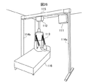
図26は、給電側装置50および受電側装置60の適用例を示した図のその5である。図26には、ベッドからの歩行が困難な被介護者向けのリフトが示してある。図26には、充電器111と、電動リフト112と、スリングシート113と、支柱114a,114bと、レール115と、ベッド116とが示してある。
FIG. 26 is a fifth diagram illustrating an application example of the power
充電器111は、図20に示した給電側装置50を有している。充電器111は、支柱114a,114bによって支えられたレール115の端の部分に取り付けられている。
The
電動リフト112は、図20に示した受電側装置60を有している。電動リフト112は、レール115に沿って移動できるように、レール115に連結されている。電動リフト112は、モータ等の駆動装置を備え、受電側装置60が備えるバッテリ65によって、レール115に沿って移動する。電動リフト112には、スリングシート113が取り付けられている。
The
電動リフト112は、レール115に沿って、充電器111の位置に来ると、電力コイル61が、充電器111の電力コイル55と対向するようになっている。これにより、電動リフト112のバッテリ65は充電される。
When the
以上説明したように、給電側装置50および受電側装置60は、充電器111および電動リフト112に適用することができる。給電側装置50および受電側装置60は、磁界漏洩を抑制するので、例えば、被介護者が装着した心臓ペースメーカや補聴器などの医療機器に対して、干渉の影響を抑制することができる。
As described above, the power
以上、本発明について実施形態を用いて説明したが、電力コイル、給電側装置、および受電側装置の構成を理解容易にするために、主な処理内容に応じて分類したものである。構成要素の分類の仕方や名称によって、本願発明が制限されることはない。電力コイル、給電側装置、および受電側装置の構成は、処理内容に応じて、さらに多くの構成要素に分類することもできる。また、1つの構成要素がさらに多くの処理を実行するように分類することもできる。また、各構成要素の処理は、1つのハードウェアで実行されてもよいし、複数のハードウェアで実行されてもよい。 As mentioned above, although this invention was demonstrated using embodiment, in order to make an understanding of the structure of a power coil, an electric power feeding side apparatus, and an electric power receiving side apparatus easy, it classified according to the main processing content. The present invention is not limited by the way of classification and names of the constituent elements. The configurations of the power coil, the power feeding side device, and the power receiving side device can be classified into more components depending on the processing content. Moreover, it can also classify | categorize so that one component may perform more processes. Further, the processing of each component may be executed by one hardware or may be executed by a plurality of hardware.
また、上述したフローチャートの各処理単位は、給電側装置および受電側装置の処理を理解容易にするために、主な処理内容に応じて分割したものである。処理単位の分割の仕方や名称によって、本願発明が制限されることはない。給電側装置および受電側装置の処理は、処理内容に応じて、さらに多くの処理単位に分割することもできる。また、1つの処理単位がさらに多くの処理を含むように分割することもできる。 In addition, each processing unit of the above-described flowchart is divided according to main processing contents in order to facilitate understanding of the processing of the power supply side device and the power reception side device. The present invention is not limited by the way of dividing the processing unit or the name. The processing of the power supply side device and the power receiving side device can be divided into a larger number of processing units depending on the processing content. Moreover, it can also divide | segment so that one process unit may contain many processes.
また、本発明の技術的範囲は上記実施形態に記載の範囲には限定されない。上記実施形態に多様な変更または改良を加えることが可能であることが当業者には明らかである。また、そのような変更または改良を加えた形態も本発明の技術的範囲に含まれ得ることが、特許請求の範囲の記載から明らかである。さらに、各実施の形態を組み合わせることもできる。 Further, the technical scope of the present invention is not limited to the scope described in the above embodiment. It will be apparent to those skilled in the art that various modifications or improvements can be made to the above embodiment. In addition, it is apparent from the scope of the claims that the embodiments added with such changes or improvements can be included in the technical scope of the present invention. Furthermore, the embodiments can be combined.
また、図面等において示した各構成の位置、大きさ、形状、範囲などは、発明の理解を容易にするため、実際の位置、大きさ、形状、範囲などを表していない場合がある。このため、本発明は、必ずしも、図面等に開示された位置、大きさ、形状、範囲などに限定されない。 In addition, the position, size, shape, range, and the like of each component illustrated in the drawings and the like may not represent the actual position, size, shape, range, or the like in order to facilitate understanding of the invention. For this reason, the present invention is not necessarily limited to the position, size, shape, range, and the like disclosed in the drawings and the like.
(付記1)
第1の内側コイルと、
一端が前記第1の内側コイルの一端と接続された第2の内側コイルと、
前記第1の内側コイルを囲うように前記第1の内側コイルの外側で第1のループを形成し、前記第1のループの外側において、前記第1の内側コイルの外側の磁束と逆相の磁束を発生する、一端が第1の端子と接続され、他端が前記第1の内側コイルの他端と接続された第1の外側コイルと、
前記第2の内側コイルを囲うように前記第2の内側コイルの外側で第2のループを形成し、前記第2のループの外側において、前記第2の内側コイルの外側の磁束と逆相の磁束を発生する、一端が第2の端子と接続され、他端が前記第2の内側コイルの他端と接続された第2の外側コイルと、
を有することを特徴とする電力コイル。
(Appendix 1)
A first inner coil;
A second inner coil having one end connected to one end of the first inner coil;
A first loop is formed outside the first inner coil so as to surround the first inner coil, and the outer side of the first loop is opposite in phase to the magnetic flux outside the first inner coil. A first outer coil that generates magnetic flux, one end connected to the first terminal and the other end connected to the other end of the first inner coil;
A second loop is formed outside the second inner coil so as to surround the second inner coil, and the outer side of the second loop is opposite in phase to the magnetic flux outside the second inner coil. A second outer coil that generates magnetic flux, one end connected to the second terminal and the other end connected to the other end of the second inner coil;
A power coil comprising:
(付記2)
増幅器と、
電源と前記増幅器との間に接続された第1のコモンモードフィルタと、
内側コイルと、前記内側コイルを囲うように形成され、外側において、前記内側コイルの外側の磁束と逆相の磁束を発生する、一端が第1の端子に接続され、他端が前記内側コイルの一端と接続された第1の外側コイルと、前記内側コイルを囲うように形成され、外側において、前記内側コイルの外側の磁束と逆相の磁束を発生する、一端が第2の端子に接続され、他端が前記内側コイルの他端と接続された第2の外側コイルと、を有する電力コイルと、
前記増幅器と前記電力コイルとの間に接続された第2のコモンモードフィルタと、
を有することを特徴とする給電側装置。
(Appendix 2)
An amplifier;
A first common mode filter connected between a power source and the amplifier;
The inner coil is formed so as to surround the inner coil, and generates a magnetic flux opposite in phase to the outer magnetic flux of the inner coil on the outer side. One end is connected to the first terminal, and the other end is connected to the inner coil. A first outer coil connected to one end and a first outer coil formed so as to surround the inner coil, and generates a magnetic flux having a phase opposite to the outer magnetic flux of the inner coil on the outer side. One end is connected to the second terminal. A second outer coil having the other end connected to the other end of the inner coil, and a power coil,
A second common mode filter connected between the amplifier and the power coil;
A power supply side device comprising:
(付記3)
内側コイルと、前記内側コイルを囲うように形成され、外側において、前記内側コイルの外側の磁束と逆相の磁束を発生する、一端が第1の端子に接続され、他端が前記内側コイルの一端と接続された第1の外側コイルと、前記内側コイルを囲うように形成され、外側において、前記内側コイルの外側の磁束と逆相の磁束を発生する、一端が第2の端子に接続され、他端が前記内側コイルの他端と接続された第2の外側コイルと、を有する電力コイルと、
前記電力コイルによって受電された電力を整流する整流回路と、
前記電力コイルと前記整流回路との間に接続されたローパスフィルタと、
を有することを特徴とする受電側装置。
(Appendix 3)
The inner coil is formed so as to surround the inner coil, and generates a magnetic flux opposite in phase to the outer magnetic flux of the inner coil on the outer side. One end is connected to the first terminal, and the other end is connected to the inner coil. A first outer coil connected to one end and a first outer coil formed so as to surround the inner coil, and generates a magnetic flux having a phase opposite to the outer magnetic flux of the inner coil on the outer side. One end is connected to the second terminal. A second outer coil having the other end connected to the other end of the inner coil, and a power coil,
A rectifier circuit for rectifying the power received by the power coil;
A low pass filter connected between the power coil and the rectifier circuit;
A power receiving side device characterized by comprising:
1…無線給電システム、2…充電器、3…携帯端末、10,10a,10b…電力コイル、11…内側コイル、12a,12b…外側コイル、13a,13b…容量素子、T11,T12…端子、21a,21b…内側コイル、22…外側コイル、23a,23b…容量素子、T21,T22…端子、31…内側コイル、32a,32b…外側コイル、33a,33b…容量素子、T31,T32…端子、41a,41b…内側コイル、42…外側コイル、43a,43b…容量素子、44…シャフト、T41,T42…端子、50…給電側装置、60…受電側装置。
DESCRIPTION OF
Claims (15)
前記内側コイルを囲うように形成され、外側において、前記内側コイルの外側の磁束と逆相の磁束を発生する、一端が第1の端子に接続され、他端が前記内側コイルの一端と接続された第1の外側コイルと、
前記内側コイルを囲うように形成され、外側において、前記内側コイルの外側の磁束と逆相の磁束を発生する、一端が第2の端子に接続され、他端が前記内側コイルの他端と接続された第2の外側コイルと、
を有することを特徴とする電力コイル。 An inner coil;
The outer coil is formed so as to surround the inner coil and generates a magnetic flux opposite in phase to the outer magnetic flux of the inner coil. One end is connected to the first terminal and the other end is connected to one end of the inner coil. A first outer coil;
Formed so as to surround the inner coil, and generates a magnetic flux opposite in phase to the outer magnetic flux of the inner coil, one end is connected to the second terminal and the other end is connected to the other end of the inner coil A second outer coil formed;
A power coil comprising:
前記第1の外側コイルおよび前記第2の外側コイルは、略同じ形状を有し、略同じ位置に配置される、
ことを特徴とする電力コイル。 The power coil according to claim 1,
The first outer coil and the second outer coil have substantially the same shape and are arranged at substantially the same position.
A power coil characterized by that.
前記内側コイル、前記第1の外側コイル、および前記第2の外側コイルは、前記第1の外側コイルの一端および前記第2の外側コイルの一端から見て、対称となるように形成される、
ことを特徴とする電力コイル。 The power coil according to claim 1,
The inner coil, the first outer coil, and the second outer coil are formed to be symmetric when viewed from one end of the first outer coil and one end of the second outer coil.
A power coil characterized by that.
前記内側コイルには、前記第1の外側コイルを流れる電流と前記第2の外側コイルに流れる電流とを加算した電流に対し、略2倍の電流が流れ、
前記第1の外側コイルおよび前記第2の外側コイルの半径は、前記内側コイルの半径に対し、略21/2倍である、
ことを特徴とする電力コイル。 The power coil according to claim 1,
In the inner coil, a current approximately twice as large as the current obtained by adding the current flowing in the first outer coil and the current flowing in the second outer coil flows.
The radius of the first outer coil and the second outer coil is approximately 21/2 times the radius of the inner coil.
A power coil characterized by that.
前記内側コイルと前記第1の外側コイルとの間に接続される第1の容量素子と、
前記内側コイルと前記第2の外側コイルとの間に接続される第2の容量素子と、
をさらに有することを特徴とする電力コイル。 The power coil according to claim 1,
A first capacitive element connected between the inner coil and the first outer coil;
A second capacitive element connected between the inner coil and the second outer coil;
The power coil further comprising:
一端が第2の端子と接続された第2の内側コイルと、
前記第1の内側コイルおよび前記第2の内側コイルを囲うように形成され、外側において、前記第1の内側コイルおよび前記第2の内側コイルの外側の磁束と逆相の磁束を発生する、一端が前記第1の内側コイルの他端と接続され、他端が前記第2の内側コイルの他端と接続された外側コイルと、
を有することを特徴とする電力コイル。 A first inner coil having one end connected to the first terminal;
A second inner coil having one end connected to the second terminal;
One end that is formed so as to surround the first inner coil and the second inner coil, and generates a magnetic flux having a phase opposite to the outer magnetic flux of the first inner coil and the second inner coil on the outer side. Is connected to the other end of the first inner coil, and the other end is connected to the other end of the second inner coil,
A power coil comprising:
前記第1の内側コイルと前記第2の内側コイルは、略同じ形状を有し、略同じ位置に配置される、
ことを特徴とする電力コイル。 The power coil according to claim 6,
The first inner coil and the second inner coil have substantially the same shape and are arranged at substantially the same position.
A power coil characterized by that.
前記第1の内側コイル、前記第2の内側コイル、および前記外側コイルは、前記第1の内側コイルの一端および前記第2の内側コイルの一端から見て、対称となるように形成される、
ことを特徴とする電力コイル。 The power coil according to claim 6,
The first inner coil, the second inner coil, and the outer coil are formed to be symmetric when viewed from one end of the first inner coil and one end of the second inner coil.
A power coil characterized by that.
前記第1の内側コイルおよび前記第2の内側コイルには、前記外側コイルを流れる電流に対し、略2倍の電流が流れ、
前記外側コイルの半径は、前記第1の内側コイルおよび前記第2の内側コイルの半径に対し、略21/2倍である、
ことを特徴とする電力コイル。 The power coil according to claim 6,
In the first inner coil and the second inner coil, a current approximately twice as large as the current flowing in the outer coil flows,
The radius of the outer coil is approximately 21/2 times the radius of the first inner coil and the second inner coil.
A power coil characterized by that.
前記第1の内側コイルと前記外側コイルとの間に接続される第1の容量素子と、
前記第2の内側コイルと前記外側コイルとの間に接続される第2の容量素子と、
をさらに有することを特徴とする電力コイル。 The power coil according to claim 6,
A first capacitive element connected between the first inner coil and the outer coil;
A second capacitive element connected between the second inner coil and the outer coil;
The power coil further comprising:
前記内側コイルの外側で第1のループを形成し、前記第1のループの外側において、前記内側コイルの外側の磁束と逆相の磁束を発生する、一端が第1の端子と接続され、他端が前記内側コイルの一端と接続された第1の外側コイルと、
前記内側コイルの外側で第2のループを形成し、前記第2のループの外側において、前記内側コイルの外側の磁束と逆相の磁束を発生する、一端が第2の端子と接続され、他端が前記内側コイルの他端と接続された第2の外側コイルと、
を有することを特徴とする電力コイル。 An inner coil;
A first loop is formed outside the inner coil, and a magnetic flux having a phase opposite to the magnetic flux outside the inner coil is generated outside the first loop. A first outer coil having an end connected to one end of the inner coil;
A second loop is formed outside the inner coil, and a magnetic flux opposite in phase to the magnetic flux outside the inner coil is generated outside the second loop. One end is connected to the second terminal, and the other A second outer coil having an end connected to the other end of the inner coil;
A power coil comprising:
前記第1のループと前記第2のループは、略同じ形状を有し、異なる位置に配置される、
ことを特徴とする電力コイル。 A power coil according to claim 11,
The first loop and the second loop have substantially the same shape and are arranged at different positions.
A power coil characterized by that.
前記内側コイル、前記第1の外側コイル、および前記第2の外側コイルは、前記第1の外側コイルの一端および前記第2の外側コイルの一端から見て、対称となるように形成される、
ことを特徴とする電力コイル。 A power coil according to claim 11,
The inner coil, the first outer coil, and the second outer coil are formed to be symmetric when viewed from one end of the first outer coil and one end of the second outer coil.
A power coil characterized by that.
前記内側コイル、前記第1の外側コイル、および前記第2の外側コイルのそれぞれには、略同じ電流が流れ、
前記内側コイルの面積は、前記第1の外側コイルの面積と前記第2の外側コイルの面積とを加算した面積と略同じである、
ことを特徴とする電力コイル。 A power coil according to claim 11,
In each of the inner coil, the first outer coil, and the second outer coil, substantially the same current flows,
The area of the inner coil is substantially the same as the area obtained by adding the area of the first outer coil and the area of the second outer coil.
A power coil characterized by that.
前記内側コイルと前記第1の外側コイルとの間に接続される第1の容量素子と、
前記内側コイルと前記第2の外側コイルとの間に接続される第2の容量素子と、
をさらに有することを特徴とする電力コイル。 A power coil according to claim 11,
A first capacitive element connected between the inner coil and the first outer coil;
A second capacitive element connected between the inner coil and the second outer coil;
The power coil further comprising:
Priority Applications (6)
| Application Number | Priority Date | Filing Date | Title |
|---|---|---|---|
| JP2016095947A JP6522546B2 (en) | 2016-05-12 | 2016-05-12 | Power coil |
| CN201780029165.3A CN109155189B (en) | 2016-05-12 | 2017-03-07 | Power coil |
| PCT/JP2017/008926 WO2017195447A1 (en) | 2016-05-12 | 2017-03-07 | Power coil |
| US16/300,176 US11581758B2 (en) | 2016-05-12 | 2017-03-07 | Power transfer coil |
| JP2019083260A JP6700455B2 (en) | 2016-05-12 | 2019-04-24 | apparatus |
| US18/104,835 US20230187978A1 (en) | 2016-05-12 | 2023-02-02 | Wireless Power Transfer Using Inductive Coupling |
Applications Claiming Priority (1)
| Application Number | Priority Date | Filing Date | Title |
|---|---|---|---|
| JP2016095947A JP6522546B2 (en) | 2016-05-12 | 2016-05-12 | Power coil |
Related Child Applications (1)
| Application Number | Title | Priority Date | Filing Date |
|---|---|---|---|
| JP2019083260A Division JP6700455B2 (en) | 2016-05-12 | 2019-04-24 | apparatus |
Publications (2)
| Publication Number | Publication Date |
|---|---|
| JP2017204576A true JP2017204576A (en) | 2017-11-16 |
| JP6522546B2 JP6522546B2 (en) | 2019-05-29 |
Family
ID=60266501
Family Applications (2)
| Application Number | Title | Priority Date | Filing Date |
|---|---|---|---|
| JP2016095947A Active JP6522546B2 (en) | 2016-05-12 | 2016-05-12 | Power coil |
| JP2019083260A Active JP6700455B2 (en) | 2016-05-12 | 2019-04-24 | apparatus |
Family Applications After (1)
| Application Number | Title | Priority Date | Filing Date |
|---|---|---|---|
| JP2019083260A Active JP6700455B2 (en) | 2016-05-12 | 2019-04-24 | apparatus |
Country Status (4)
| Country | Link |
|---|---|
| US (2) | US11581758B2 (en) |
| JP (2) | JP6522546B2 (en) |
| CN (1) | CN109155189B (en) |
| WO (1) | WO2017195447A1 (en) |
Cited By (2)
| Publication number | Priority date | Publication date | Assignee | Title |
|---|---|---|---|---|
| WO2020195587A1 (en) * | 2019-03-25 | 2020-10-01 | オムロン株式会社 | Power transfer device |
| WO2021070519A1 (en) * | 2019-10-11 | 2021-04-15 | 株式会社オートネットワーク技術研究所 | Power supply device |
Families Citing this family (18)
| Publication number | Priority date | Publication date | Assignee | Title |
|---|---|---|---|---|
| US10714960B2 (en) * | 2015-12-22 | 2020-07-14 | Intel Corporation | Uniform wireless charging device |
| KR102589290B1 (en) * | 2016-06-30 | 2023-10-13 | 엘지이노텍 주식회사 | Wireless power transmission coil arranging method and the coil |
| US10790700B2 (en) * | 2018-05-18 | 2020-09-29 | Tectus Corporation | Power generation necklaces with field shaping systems |
| KR102645042B1 (en) * | 2018-09-14 | 2024-03-08 | 현대자동차주식회사 | Reconfigurable electromagnetic wave shielding filter, wireless charger for vehicle having the same, and control method thereof |
| CN210041438U (en) * | 2018-12-03 | 2020-02-07 | 邢益涛 | Wireless energy transmission device with noise reduction design |
| US11831173B2 (en) | 2021-11-03 | 2023-11-28 | Nucurrent, Inc. | Wireless power transmission antenna with series coil molecule configuration |
| US11824372B2 (en) | 2021-11-03 | 2023-11-21 | Nucurrent, Inc. | Wireless power transmission antenna with puzzled antenna molecules |
| US11831175B2 (en) | 2021-11-03 | 2023-11-28 | Nucurrent, Inc. | Wireless power transmission antenna with antenna molecules |
| US11962337B2 (en) | 2021-11-03 | 2024-04-16 | Nucurrent, Inc. | Communications demodulation in wireless power transmission system having an internal repeater |
| US11862991B2 (en) | 2021-11-03 | 2024-01-02 | Nucurrent, Inc. | Wireless power transmission antenna with internal repeater and in-coil tuning |
| US11831176B2 (en) | 2021-11-03 | 2023-11-28 | Nucurrent, Inc. | Wireless power transfer systems with substantial uniformity over a large area |
| US11848566B2 (en) | 2021-11-03 | 2023-12-19 | Nucurrent, Inc. | Dual communications demodulation of a wireless power transmission system having an internal repeater |
| US11824373B2 (en) | 2021-11-03 | 2023-11-21 | Nucurrent, Inc. | Wireless power transmission antenna with parallel coil molecule configuration |
| US11824371B2 (en) | 2021-11-03 | 2023-11-21 | Nucurrent, Inc. | Wireless power transmission antenna with internal repeater and repeater filter |
| US11831177B2 (en) * | 2021-11-03 | 2023-11-28 | Nucurrent, Inc. | Wireless power transmitter with internal repeater and enhanced uniformity |
| US11862984B2 (en) | 2021-11-03 | 2024-01-02 | Nucurrent, Inc. | Wireless power receiver with repeater for enhanced power harvesting |
| US11955819B2 (en) | 2021-11-03 | 2024-04-09 | Nucurrent, Inc. | Communications modulation in wireless power receiver with multi-coil receiver antenna |
| US20230136343A1 (en) * | 2021-11-03 | 2023-05-04 | Nucurrent, Inc. | Wireless Power Transmission Antenna with Internal Repeater and Inter-Turn Emissions Mitigation |
Citations (9)
| Publication number | Priority date | Publication date | Assignee | Title |
|---|---|---|---|---|
| JPH1132452A (en) * | 1997-05-15 | 1999-02-02 | Hitachi Ltd | Reader and/or writer |
| JP2003037950A (en) * | 2001-07-26 | 2003-02-07 | Matsushita Electric Works Ltd | Non-contact power transmission device |
| JP2012244763A (en) * | 2011-05-19 | 2012-12-10 | Sony Corp | Power supply device, power supply system and electronic device |
| US20130187474A1 (en) * | 2008-07-02 | 2013-07-25 | Access Business Group International Llc | Electromagnetic interference mitigation |
| JP2013243431A (en) * | 2012-05-17 | 2013-12-05 | Equos Research Co Ltd | Antenna coil |
| WO2013179639A1 (en) * | 2012-05-28 | 2013-12-05 | パナソニック株式会社 | Contactless connector system |
| JP2015012702A (en) * | 2013-06-28 | 2015-01-19 | 株式会社エクォス・リサーチ | Antenna coil unit |
| JP2015089259A (en) * | 2013-10-31 | 2015-05-07 | 株式会社エクォス・リサーチ | Antenna coil unit |
| WO2016162964A1 (en) * | 2015-04-08 | 2016-10-13 | 日産自動車株式会社 | Ground-side coil unit |
Family Cites Families (13)
| Publication number | Priority date | Publication date | Assignee | Title |
|---|---|---|---|---|
| US6176433B1 (en) | 1997-05-15 | 2001-01-23 | Hitachi, Ltd. | Reader/writer having coil arrangements to restrain electromagnetic field intensity at a distance |
| KR100819604B1 (en) * | 2005-07-27 | 2008-04-03 | 엘에스전선 주식회사 | Wireless Charger Decreased in Variation of Charging Efficiency |
| KR101134625B1 (en) * | 2010-07-16 | 2012-04-09 | 주식회사 한림포스텍 | Core assembly for wireless power transmission, power supplying apparatus for wireless power transmission having the same, and method for manufacturing core assembly for wireless power transmission |
| JP5532422B2 (en) * | 2010-07-30 | 2014-06-25 | スミダコーポレーション株式会社 | coil |
| US10685780B2 (en) * | 2011-03-29 | 2020-06-16 | Sony Corporation | Electric power feed apparatus, electric power feed system, and electronic apparatus |
| JPWO2014111971A1 (en) * | 2013-01-16 | 2017-01-19 | 三重電子株式会社 | Contactless transmission device |
| JP2015015852A (en) | 2013-07-05 | 2015-01-22 | 株式会社エクォス・リサーチ | Coil antenna |
| KR102122394B1 (en) * | 2013-08-08 | 2020-06-15 | 삼성전자주식회사 | Method and apparatus of wireless power transmission for efficient power distribution |
| JP6164421B2 (en) * | 2013-11-28 | 2017-07-19 | Tdk株式会社 | Power transmission coil unit and wireless power transmission device |
| JP6281963B2 (en) | 2014-02-24 | 2018-02-21 | 光電子株式会社 | Non-contact power transmission device and non-contact power transmission method |
| US9779868B2 (en) * | 2014-04-30 | 2017-10-03 | Qorvo Us, Inc. | Compact impedance transformer |
| KR102450606B1 (en) * | 2015-09-25 | 2022-10-05 | 주식회사 위츠 | Apparatus for receiving power wirelessly and power supply apparatus using the same |
| KR20170041389A (en) * | 2015-10-07 | 2017-04-17 | 엘지이노텍 주식회사 | Method for Guiding Alignment of Wireless Charging Device, Apparatus and System therefor |
-
2016
- 2016-05-12 JP JP2016095947A patent/JP6522546B2/en active Active
-
2017
- 2017-03-07 WO PCT/JP2017/008926 patent/WO2017195447A1/en active Application Filing
- 2017-03-07 CN CN201780029165.3A patent/CN109155189B/en active Active
- 2017-03-07 US US16/300,176 patent/US11581758B2/en active Active
-
2019
- 2019-04-24 JP JP2019083260A patent/JP6700455B2/en active Active
-
2023
- 2023-02-02 US US18/104,835 patent/US20230187978A1/en active Pending
Patent Citations (9)
| Publication number | Priority date | Publication date | Assignee | Title |
|---|---|---|---|---|
| JPH1132452A (en) * | 1997-05-15 | 1999-02-02 | Hitachi Ltd | Reader and/or writer |
| JP2003037950A (en) * | 2001-07-26 | 2003-02-07 | Matsushita Electric Works Ltd | Non-contact power transmission device |
| US20130187474A1 (en) * | 2008-07-02 | 2013-07-25 | Access Business Group International Llc | Electromagnetic interference mitigation |
| JP2012244763A (en) * | 2011-05-19 | 2012-12-10 | Sony Corp | Power supply device, power supply system and electronic device |
| JP2013243431A (en) * | 2012-05-17 | 2013-12-05 | Equos Research Co Ltd | Antenna coil |
| WO2013179639A1 (en) * | 2012-05-28 | 2013-12-05 | パナソニック株式会社 | Contactless connector system |
| JP2015012702A (en) * | 2013-06-28 | 2015-01-19 | 株式会社エクォス・リサーチ | Antenna coil unit |
| JP2015089259A (en) * | 2013-10-31 | 2015-05-07 | 株式会社エクォス・リサーチ | Antenna coil unit |
| WO2016162964A1 (en) * | 2015-04-08 | 2016-10-13 | 日産自動車株式会社 | Ground-side coil unit |
Cited By (7)
| Publication number | Priority date | Publication date | Assignee | Title |
|---|---|---|---|---|
| WO2020195587A1 (en) * | 2019-03-25 | 2020-10-01 | オムロン株式会社 | Power transfer device |
| JP2020162228A (en) * | 2019-03-25 | 2020-10-01 | オムロン株式会社 | Power transmission device |
| US11456626B2 (en) | 2019-03-25 | 2022-09-27 | Omron Corporation | Power transfer device |
| JP7259467B2 (en) | 2019-03-25 | 2023-04-18 | オムロン株式会社 | power transmission equipment |
| WO2021070519A1 (en) * | 2019-10-11 | 2021-04-15 | 株式会社オートネットワーク技術研究所 | Power supply device |
| JP2021065013A (en) * | 2019-10-11 | 2021-04-22 | 株式会社オートネットワーク技術研究所 | Power supply device |
| JP7255445B2 (en) | 2019-10-11 | 2023-04-11 | 株式会社オートネットワーク技術研究所 | power supply |
Also Published As
| Publication number | Publication date |
|---|---|
| JP6700455B2 (en) | 2020-05-27 |
| JP6522546B2 (en) | 2019-05-29 |
| WO2017195447A1 (en) | 2017-11-16 |
| US11581758B2 (en) | 2023-02-14 |
| CN109155189A (en) | 2019-01-04 |
| US20230187978A1 (en) | 2023-06-15 |
| CN109155189B (en) | 2020-11-10 |
| JP2019193563A (en) | 2019-10-31 |
| US20190173325A1 (en) | 2019-06-06 |
Similar Documents
| Publication | Publication Date | Title |
|---|---|---|
| JP6700455B2 (en) | apparatus | |
| CN104681257B (en) | Power transmission coil unit and Contactless power transmission device | |
| US9548621B2 (en) | Contactless connector system tolerant of position displacement between transmitter coil and receiver coil and having high transmission efficiency | |
| KR101230211B1 (en) | Non-contact power feeding apparatus of magnetic resonance method | |
| JP6845624B2 (en) | Power transmission device, power receiving device and contactless power supply system | |
| US20150137612A1 (en) | Antenna coil | |
| JP2017526323A (en) | Resonator balancing in wireless power transfer systems | |
| JPWO2014038148A1 (en) | Contactless power supply system and contactless extension plug | |
| JP2013208012A (en) | Antenna coil unit and magnetic field resonance power supply system | |
| JP2012049434A (en) | Electronic component, feeder device, power receiver, and wireless feeder system | |
| US20160043575A1 (en) | Wireless power transmission system | |
| US20180082782A1 (en) | Ground-side coil unit | |
| US20170126059A1 (en) | Contactless power supply system supplying power using power supply pad in contact less manner | |
| WO2017183393A1 (en) | Power reception device | |
| JP6895725B2 (en) | Power transmission device | |
| JP6305728B2 (en) | Coil unit and power transmission system | |
| JP6600607B2 (en) | Inductor unit, wireless power transmission device, electric vehicle, and charging facility | |
| US20110234337A1 (en) | Filter circuit for differential communication | |
| CN108574327A (en) | Coil unit, wireless power supply, wireless receiving device and Wireless power transmission system | |
| JP2019180203A (en) | Device and system for wireless power transmission | |
| JP2015089259A (en) | Antenna coil unit | |
| JP2016111756A (en) | Non-contact power transmission device and non-contact power reception device | |
| US20140054972A1 (en) | Wireless power transmission system | |
| JP2024042725A (en) | Matching circuit for wireless power receiving device | |
| WO2014069331A1 (en) | Contactless power feeding device |
Legal Events
| Date | Code | Title | Description |
|---|---|---|---|
| A711 | Notification of change in applicant |
Free format text: JAPANESE INTERMEDIATE CODE: A712 Effective date: 20171120 |
|
| A521 | Request for written amendment filed |
Free format text: JAPANESE INTERMEDIATE CODE: A821 Effective date: 20171120 |
|
| A621 | Written request for application examination |
Free format text: JAPANESE INTERMEDIATE CODE: A621 Effective date: 20181108 |
|
| RD02 | Notification of acceptance of power of attorney |
Free format text: JAPANESE INTERMEDIATE CODE: A7422 Effective date: 20181108 |
|
| TRDD | Decision of grant or rejection written | ||
| A01 | Written decision to grant a patent or to grant a registration (utility model) |
Free format text: JAPANESE INTERMEDIATE CODE: A01 Effective date: 20190326 |
|
| A61 | First payment of annual fees (during grant procedure) |
Free format text: JAPANESE INTERMEDIATE CODE: A61 Effective date: 20190424 |
|
| R150 | Certificate of patent or registration of utility model |
Ref document number: 6522546 Country of ref document: JP Free format text: JAPANESE INTERMEDIATE CODE: R150 |
|
| S111 | Request for change of ownership or part of ownership |
Free format text: JAPANESE INTERMEDIATE CODE: R313111 |
|
| R350 | Written notification of registration of transfer |
Free format text: JAPANESE INTERMEDIATE CODE: R350 |
|
| R250 | Receipt of annual fees |
Free format text: JAPANESE INTERMEDIATE CODE: R250 |
|
| R250 | Receipt of annual fees |
Free format text: JAPANESE INTERMEDIATE CODE: R250 |