JP2017201751A - A/d converter - Google Patents
A/d converter Download PDFInfo
- Publication number
- JP2017201751A JP2017201751A JP2016092820A JP2016092820A JP2017201751A JP 2017201751 A JP2017201751 A JP 2017201751A JP 2016092820 A JP2016092820 A JP 2016092820A JP 2016092820 A JP2016092820 A JP 2016092820A JP 2017201751 A JP2017201751 A JP 2017201751A
- Authority
- JP
- Japan
- Prior art keywords
- reference voltage
- value
- conversion
- input
- gain stage
- Prior art date
- Legal status (The legal status is an assumption and is not a legal conclusion. Google has not performed a legal analysis and makes no representation as to the accuracy of the status listed.)
- Granted
Links
Images


Abstract
Description
本発明は、A/D変換器に関する。 The present invention relates to an A / D converter.
特許文献1には、A/D変換器が記載されている。このA/D変換器は、まず、入力されたアナログ信号に対してフォールディング積分型A/D変換を行う。次に、A/D変換器は、フォールディング積分型A/D変換の残差アナログ信号に対して巡回型A/D変換を行う。フォールディング積分型及び巡回型のA/D変換動作を行うA/D変換器(いわゆるFICC型A/D変換器)によれば、フォールディング積分によって読み出しノイズを抑制すると共に、グレースケールの分解能を高めることができる。
FICC型A/D変換器は、例えば、CMOSイメージセンサに用いられる。CMOSイメージセンサのカラムピッチは微細である。そこで、FICC型A/D変換器をCMOSイメージセンサに実装するために、フォールディング積分動作を行う素子として1ビットサブA/D変換回路を採用し得る。1ビットサブA/D変換回路は、1ビットのディジタル値を生成する。 The FICC type A / D converter is used for a CMOS image sensor, for example. The column pitch of the CMOS image sensor is fine. Therefore, in order to mount the FICC type A / D converter in the CMOS image sensor, a 1-bit sub A / D conversion circuit can be adopted as an element for performing a folding integration operation. The 1-bit sub A / D conversion circuit generates a 1-bit digital value.
FICC型A/D変換器は、上記した1ビットサブA/D変換回路や演算増幅回路などを構成要素として含む。これらの要素は、電圧オフセットやゲインのずれといった誤差要因を含む。これらの誤差は、フォールディング積分動作が繰り返される毎に蓄積されて、フォールディング積分動作の結果としての残差アナログ信号に含まれる。そして、巡回型A/D変換動作には、蓄積された誤差を含む残差アナログ信号が提供されてしまう。その結果、巡回型A/D変換動作へ提供される信号の大きさが、巡回型A/D変換動作が受け入れ可能な範囲を超えることがあり得る。 The FICC A / D converter includes the above-described 1-bit sub A / D conversion circuit, operational amplifier circuit, and the like as constituent elements. These factors include error factors such as voltage offset and gain shift. These errors are accumulated each time the folding integration operation is repeated, and are included in the residual analog signal as a result of the folding integration operation. In the cyclic A / D conversion operation, a residual analog signal including an accumulated error is provided. As a result, the magnitude of the signal provided to the cyclic A / D conversion operation may exceed the range acceptable for the cyclic A / D conversion operation.
そこで、本発明は、積分演算の結果を所望の範囲に収めることにより良好なA/D変換特性を得ることが可能なA/D変換器を提供することを目的とする。 Accordingly, an object of the present invention is to provide an A / D converter capable of obtaining a good A / D conversion characteristic by keeping the result of integration calculation within a desired range.
本発明の一形態は、入力信号の標本化及び標本値の積分を繰り返し行うことによりアナログ信号からディジタル値を得るためのフォールディング積分型の動作を含むA/D変換動作を行うA/D変換器であって、ディジタル値に変換されるアナログ信号を受ける入力、アナログ信号に基づく信号を生成する演算増幅回路、及び、演算増幅回路において生成された信号を送出する出力、を含むゲインステージと、ゲインステージの入力に提供されるアナログ信号、又は、ゲインステージの出力から送出される信号に基づき、変換参照電圧を生成する参照電圧発生部と、ゲインステージの出力からの信号に基づき、参照電圧発生部から提供される変換参照電圧を参照して、1ビットのディジタル値を生成可能な比較器を含むA/D変換回路と、を備える。 One embodiment of the present invention is an A / D converter that performs an A / D conversion operation including a folding integration type operation for obtaining a digital value from an analog signal by repeatedly sampling an input signal and integrating a sample value. A gain stage including an input for receiving an analog signal to be converted into a digital value, an operational amplifier circuit for generating a signal based on the analog signal, and an output for transmitting the signal generated in the operational amplifier circuit; A reference voltage generator for generating a conversion reference voltage based on an analog signal provided to the input of the stage or a signal sent from the output of the gain stage, and a reference voltage generator based on the signal from the output of the gain stage An A / D conversion circuit including a comparator capable of generating a 1-bit digital value with reference to the conversion reference voltage provided by Obtain.
このA/D変換器では、参照電圧発生部がゲインステージの入力に提供される信号、又は、ゲインステージの出力から送出される信号に基づいて変換参照電圧を生成する。そして、当該変換参照電圧を参照して、ゲインステージからの信号がディジタル値に変換される。これにより、変換参照電圧は、可変値であるので、積分動作の繰り返しによってもゲインステージの出力から送出される信号が所望の範囲を超えないようにすることが可能になる。従って、このA/D変換器では、積分演算の結果が所望の範囲に収められるので、良好なA/D変換特性を得ることができる。 In this A / D converter, the reference voltage generator generates a converted reference voltage based on a signal provided to the input of the gain stage or a signal sent from the output of the gain stage. Then, the signal from the gain stage is converted into a digital value with reference to the conversion reference voltage. Thus, since the conversion reference voltage is a variable value, it is possible to prevent the signal sent from the output of the gain stage from exceeding the desired range even by repeating the integration operation. Therefore, in this A / D converter, the result of the integral calculation is within a desired range, and thus a good A / D conversion characteristic can be obtained.
演算増幅回路は、第1の入力、第2の入力、及び出力を有し、ゲインステージは、第1の入力に接続可能な第1のキャパシタと、第1の入力に接続可能な第2のキャパシタと、第1の入力と出力との間に接続される第3のキャパシタと、を有し、第3のキャパシタの容量は、第1のキャパシタの容量及び第2のキャパシタの容量の2倍であり、参照電圧発生部は、2回目のフォールディング積分動作で得られたゲインステージから送出される信号に基づき、変換参照電圧を生成し、A/D変換回路は、(n+1)回目(nは2以上の整数)のフォールディング積分動作で得られたゲインステージからの信号に基づき、2回目のフォールディング積分動作で得られたゲインステージからの信号に基づく変換参照電圧を参照して、ディジタル値を生成してもよい。 The operational amplifier circuit has a first input, a second input, and an output, and the gain stage has a first capacitor connectable to the first input and a second capacitor connectable to the first input. A capacitor and a third capacitor connected between the first input and the output, wherein the capacitance of the third capacitor is twice the capacitance of the first capacitor and the capacitance of the second capacitor. The reference voltage generation unit generates a conversion reference voltage based on the signal sent from the gain stage obtained by the second folding integration operation, and the A / D conversion circuit performs the (n + 1) th (n is Based on the signal from the gain stage obtained by the folding integration operation of 2 or more), refer to the conversion reference voltage based on the signal from the gain stage obtained by the second folding integration operation, It may form.
このゲインステージでは、第3のキャパシタの容量が、第1のキャパシタの容量及び第2のキャパシタの容量の2倍である。換言すると、第1のキャパシタ及び第2のキャパシタと、第3のキャパシタとの容量比が1/2である。従って、演算増幅回路における電圧の出力範囲は、入力範囲の1/2になる。このため、このゲインステージによれば、1回目の積分動作によって入力信号の大きさが1/2となる。次に、2回目の積分動作では1回目の積分動作の結果と、1/2とされる演算増幅回路の出力とが足し合される。従って、2回目の積分動作の出力範囲は、入力信号の範囲に対応する。これにより、変換参照電圧の生成において、2回目の積分動作の出力を参照することは、入力を参照することと同じ意味である。従って、ゲインステージの出力を利用して、積分演算の結果を所望の範囲に収めることが可能な変換参照電圧を生成することができる。 In this gain stage, the capacity of the third capacitor is twice the capacity of the first capacitor and the capacity of the second capacitor. In other words, the capacitance ratio of the first capacitor, the second capacitor, and the third capacitor is ½. Therefore, the voltage output range in the operational amplifier circuit is ½ of the input range. For this reason, according to this gain stage, the magnitude of the input signal is halved by the first integration operation. Next, in the second integration operation, the result of the first integration operation is added to the output of the operational amplifier circuit that is halved. Therefore, the output range of the second integration operation corresponds to the input signal range. Thus, referring to the output of the second integration operation in generating the conversion reference voltage has the same meaning as referring to the input. Therefore, it is possible to generate a conversion reference voltage that can use the output of the gain stage to keep the result of the integration calculation within a desired range.
A/D変換回路において生成されたディジタル値に応じて、制御信号を生成する論理回路と、第1の基準参照電圧及び第2の基準参照電圧の少なくとも何れか一方を、制御信号に応じてゲインステージに提供するD/A変換回路と、をさらに備え、参照電圧発生部は、2回目の積分動作で得られたゲインステージから送出される信号の大きさと、第1の基準参照電圧及び第2の基準参照電圧に基づく第1の閾値と、の比較により、ゲインステージから送出される信号が第1の閾値以上である場合に生成される第1の制御値、又は、ゲインステージから送出される信号が第1の閾値未満である場合に生成される第2の制御値に基づき、第1の制御値であるとき、第1の閾値と第1の制御値とに基づいて第2の閾値を生成し、第2の制御値であるとき、第1の閾値と第2の制御値とに基づいて第3の閾値を生成し、第2の閾値は、第1の閾値より小さく、第3の閾値は、第1の閾値より大きく、(n+1)回目(nは2以上の整数)のフォールディング積分動作で得られたゲインステージから送出される信号の大きさと、第2の閾値又は第3の閾値と、を比較した結果に基づき、変換参照電圧を生成する。 A logic circuit that generates a control signal in accordance with a digital value generated in the A / D conversion circuit, and at least one of the first reference voltage and the second reference voltage is gained according to the control signal. A D / A conversion circuit provided to the stage, and the reference voltage generation unit is configured to output the magnitude of the signal transmitted from the gain stage obtained by the second integration operation, the first reference reference voltage, and the second reference voltage. The first control value generated when the signal sent from the gain stage is greater than or equal to the first threshold value by comparison with the first threshold value based on the reference reference voltage, or sent from the gain stage Based on the second control value generated when the signal is less than the first threshold, and when the signal is the first control value, the second threshold is determined based on the first threshold and the first control value. Generated and is the second control value A third threshold value is generated based on the first threshold value and the second control value, the second threshold value is smaller than the first threshold value, the third threshold value is larger than the first threshold value, Based on the result of comparing the magnitude of the signal transmitted from the gain stage obtained in the (n + 1) -th (n is an integer equal to or greater than 2) folding integration operation with the second threshold or the third threshold. Generate a reference voltage.
参照電圧発生部は、2回目の積分動作で得られたゲインステージの出力に基づいて、第1の制御値又は第2の制御値を生成する。そして、参照電圧発生部は、3回目の積分動作で得られたゲインステージの出力をA/D変換するための変換参照電圧を、第2の閾値又は第3の閾値に基づいて生成する。この第2の閾値は、第1の閾値及び第1の制御値に基づいて生成され、第3の閾値は第1の閾値及び第2の制御値に基づいて生成される。そして、第2の閾値は、第1の閾値より小さい。一方、第3の閾値は、第1の閾値より大きい。その結果、ゲインステージの出力が大きい場合にはA/D変換回路に提供される閾値が小さくなり、ゲインステージの出力が小さい場合にはA/D変換回路に提供される閾値が大きくなる。ここで、閾値は、ゲインステージの出力を所定の範囲に収めるために、当該出力から所定の値を減じる動作(いわゆる折り返し動作)を行うか否かを判断するための値である。そうすると、第2の閾値が第1の閾値より小さい場合には、ゲインステージの出力が小さい段階で折り返し動作が実行されることになる。従って、ゲインステージの出力から上限値までの間に余裕を設けることが可能になる。また、第3の閾値が第1の閾値より大きい場合には、ゲインステージの出力が大きい段階で折り返し動作が実行されることになる。従って、ゲインステージの出力から下限値までの間に余裕を設けることが可能になる。 The reference voltage generator generates the first control value or the second control value based on the output of the gain stage obtained by the second integration operation. The reference voltage generation unit generates a conversion reference voltage for A / D converting the output of the gain stage obtained by the third integration operation based on the second threshold or the third threshold. The second threshold value is generated based on the first threshold value and the first control value, and the third threshold value is generated based on the first threshold value and the second control value. The second threshold value is smaller than the first threshold value. On the other hand, the third threshold is larger than the first threshold. As a result, when the gain stage output is large, the threshold value provided to the A / D conversion circuit is small, and when the gain stage output is small, the threshold value provided to the A / D conversion circuit is large. Here, the threshold value is a value for determining whether or not to perform an operation of reducing a predetermined value from the output (so-called folding operation) in order to keep the output of the gain stage within a predetermined range. Then, when the second threshold value is smaller than the first threshold value, the folding operation is executed when the output of the gain stage is small. Accordingly, it is possible to provide a margin between the output of the gain stage and the upper limit value. Further, when the third threshold value is larger than the first threshold value, the folding operation is executed at a stage where the output of the gain stage is large. Accordingly, a margin can be provided between the output of the gain stage and the lower limit value.
第1の基準参照電圧は、第2の基準参照電圧よりも大きく、第1の閾値は、第1の基準参照電圧と、第2の基準参照電圧との中間値であってもよい。この構成によれば、ゲインステージに入力される信号の許容範囲において、第1の閾値よりも小さい第2の閾値を用いてA/D変換される範囲と、第1の閾値よりも大きい第2の閾値を用いてA/D変換される範囲と、の境界を、入力の許容範囲の中間に設定することができる。 The first standard reference voltage is greater than the second standard reference voltage, and the first threshold value may be an intermediate value between the first standard reference voltage and the second standard reference voltage. According to this configuration, in an allowable range of a signal input to the gain stage, a range that is A / D converted using a second threshold value that is smaller than the first threshold value, and a second value that is larger than the first threshold value. The boundary between the A / D-converted range and the threshold value can be set in the middle of the input allowable range.
第1の基準参照電圧は、第2の基準参照電圧よりも大きく、第1の閾値は、第1の基準参照電圧と、第2の基準参照電圧との中間値よりも小さく、且つ、第2の基準参照電圧よりも大きくてもよい。この構成によれば、第1の閾値よりも小さい第2の閾値を用いてA/D変換される範囲と、第1の閾値よりも大きい第3の閾値を用いてA/D変換される範囲と、の境界を、入力の許容範囲における下限寄りに設定することができる。 The first standard reference voltage is greater than the second standard reference voltage, the first threshold is smaller than an intermediate value between the first standard reference voltage and the second standard reference voltage, and the second threshold It may be larger than the standard reference voltage. According to this configuration, a range that is A / D converted using a second threshold value that is smaller than the first threshold value, and a range that is A / D converted using a third threshold value that is larger than the first threshold value. Can be set closer to the lower limit in the input allowable range.
第1の基準参照電圧は、第2の基準参照電圧よりも大きく、第1の閾値は、第1の基準参照電圧と、第2の基準参照電圧との中間値よりも大きく、且つ、第1の基準参照電圧よりも小さくてもよい。この構成によれば、第1の閾値よりも小さい第3の閾値を用いてA/D変換される範囲と、第1の閾値よりも大きい第3の閾値を用いてA/D変換される範囲と、の境界を、入力の許容範囲における上限寄りに設定することができる。 The first standard reference voltage is greater than the second standard reference voltage, the first threshold is greater than an intermediate value between the first standard reference voltage and the second standard reference voltage, and the first threshold It may be smaller than the standard reference voltage. According to this configuration, a range that is A / D converted using a third threshold that is smaller than the first threshold and a range that is A / D converted using a third threshold that is larger than the first threshold. Can be set closer to the upper limit in the input allowable range.
本発明によれば、積分演算の結果を所望の範囲に収めることにより良好なA/D変換特性を得ることが可能なA/D変換器が提供される。 ADVANTAGE OF THE INVENTION According to this invention, the A / D converter which can acquire a favorable A / D conversion characteristic by keeping the result of integral calculation in the desired range is provided.
本発明の知見は、例示として示された添付図面を参照して以下の詳細な記述を考慮することによって容易に理解できる。引き続いて、添付図面を参照しながら、本発明の一形態であるA/D変換器の実施の形態を説明する。可能な場合には、同一の部分には同一の符号を付し、重複する説明を省略する。 The knowledge of the present invention can be easily understood by considering the following detailed description with reference to the accompanying drawings shown as examples. Subsequently, an embodiment of an A / D converter according to an embodiment of the present invention will be described with reference to the accompanying drawings. If possible, the same parts are denoted by the same reference numerals, and redundant description is omitted.
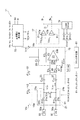
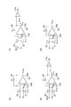
図1は、本発明の一形態に係るA/D変換器の回路図である。A/D変換器11は、いわゆるフォールディング積分型のA/D変換である第1のA/D変換動作と、巡回型A/D変換である第2のA/D変換動作を、同一の回路構成を用いて実施する。A/D変換器11は、当該A/D変換器11が有するスイッチの時系列の制御パターンの変更により、第1のA/D変換動作及び第2のA/D変換動作を実現する。
FIG. 1 is a circuit diagram of an A / D converter according to an embodiment of the present invention. The A /
図1に示されるように、A/D変換器11は、ゲインステージ15と、A/D変換回路17と、論理回路19と、D/A変換回路21と、クロック発生器61と、参照電圧発生部70と、を含む。
As shown in FIG. 1, the A /
<ゲインステージ>
ゲインステージ15は、ディジタル値に変換されるアナログ信号である入力値VINを受ける入力15aと、演算値VOPを送出する出力15bと、を含む。また、ゲインステージ15は、シングルエンド型の演算増幅回路23と、第1のキャパシタ25と、第2のキャパシタ27と、第3のキャパシタ29と、を含む。
<Gain stage>
The
演算増幅回路23は、第1の入力23aと、出力23bと、第2の入力23cと、を含む。出力23bから送出される信号の位相は、第1の入力23aに与えられた信号の位相に対して反転する。例えば、第1の入力23aは反転入力端子である。第2の入力23cは、非反転入力端子である。例えば、演算増幅回路23の第2の入力23cは、基準電位線LCOMに接続される。従って、第2の入力23cは、基準電位VCOMを受ける。
The
第1のキャパシタ25、第2のキャパシタ27及び第3のキャパシタ29は、各種の信号値の格納及び演算のための容量である。第3のキャパシタ29の容量C2は、第1のキャパシタ25の容量C1aより大きい。また、第3のキャパシタ29の容量C2は、第2のキャパシタ27の容量C1bより大きい。これら容量C1a及び容量C1bによれば、フォールディング積分型A/D変換である第1のA/D変換動作において入力される入力値VINは、容量比(C1a/C2,C1b/C2)に従って減衰される。従って、フォールディング積分型A/D変換において出力される入力値VINの電圧範囲は、キャパシタの容量比に従って小さくなる。このような構成により、シングルエンド構成の当該A/D変換器11を構成できる。
The
より詳細には、第3のキャパシタ29の容量C2は、第1のキャパシタ25の容量C1aの2倍である。また、第3のキャパシタ29の容量C2は、第2のキャパシタ27の容量C1bの2倍である。すなわち、C1a=1/2×C2及びC1b=1/2×C2といった関係が成立する。このようなキャパシタを有するA/D変換器11によれば、フォールディング積分型A/D変換において入力される入力値VINは、1/2に減衰される。そして、減衰された入力値VINがサンプリング及び積分される。従って、フォールディング積分型A/D変換において出力されるアナログ信号である演算値VOPの電圧範囲は、キャパシタの容量比に従って1/2となる。これにより、巡回型A/D変換である第2のA/D変換動作において、シングルエンド構成のA/D変換器に適した入力電圧が提供される。
More specifically, the capacitance C 2 of the
ゲインステージ15は、複数のスイッチ43,47,49,51,53を含む。複数のスイッチ43,47,49,51,53は、第1のキャパシタ25、第2のキャパシタ27及び第3のキャパシタ29を、演算増幅回路23に接続する。なお、図1に示されるスイッチ43,47,49,51,53の配置は一例である。スイッチ43,47,49,51,53は、クロック発生器61において生成される制御信号により制御される。
The
<A/D変換回路>
A/D変換回路17は、ゲインステージ15の出力15bからの演算値VOPに基づき、第1の変換参照電圧VRCH及び/又は第2の変換参照電圧VRCLに応じてディジタル値Dを生成する。
<A/D conversion circuit>
The A /
A/D変換回路17は、例えば2個のコンパレータ17a,17b(比較器)を含む。A/D変換器17は、コンパレータ17a,17bのいずれか一方を用いて1ビットのディジタル値Dを生成する。また、A/D変換器17は、コンパレータ17a,17bの両方を用いて2ビットのディジタル値Dを生成する。
The A /
コンパレータ17aは、アナログ信号と第1の変換参照電圧VRCHと比較することにより、比較結果信号であるビット(B1)を生成する。コンパレータ17bは、アナログ信号を第2の変換参照電圧VRCLと比較することにより、比較結果信号であるビット(B0)を生成する。第1の変換参照電圧VRCH及び第2の変換参照電圧VRCLは、後述する参照電圧発生部70から提供される。ディジタル値Dは、A/D変換値を示す。ディジタル値Dは、例えば1ビット(B0)又は2ビット(B0,B1)である。各ビット(B0,B1)は、「1」又は「0」を取り得る。1ビットのディジタル値Dは、(B1)である。2ビットのディジタル値Dは、(B0+B1)である。
The
なお、コンパレータ17aにおいて、第1の変換参照電圧VRCHが提供される入力は、キャパシタ(不図示)を介して基準電位VCOMに接続されてもよい。この構成によれば、高周波ノイズのためのフィルタリングを行うことが可能になる。
In the
A/D変換回路17が1ビットのディジタル値Dを生成するとき、ビット(B1)の値により1回の積分動作又は一巡回毎のディジタル値Dは、2値(D=0又はD=1)を取り得る。このとき、A/D変換回路17では、コンパレータ17aが動作する。従って、1ビットのディジタル値Dを生成するときに基準として用いられる信号は、第1の変換参照電圧VRCHである。この場合には、コンパレータ17aは、以下のように動作する。
VOP≧VRCHのとき B1=1
VOP<VRCHのとき B1=0
When the A /
When V OP ≧ V RCH B 1 = 1
When V OP <V RCH B 1 = 0
A/D変換回路17が2ビットのディジタル値Dを生成するとき、ビット(B0,B1)の組み合わせにより1回の積分動作又は一巡回毎のディジタル値Dが(D=0,D=1,D=2)を取り得る。この場合、コンパレータ17a,17bは、以下のように動作する。
VOP>VRCHのとき B1=1,B0=1
VRCL<VOP≦VRCHのとき B1=0,B0=1
VOP≦VRCLのとき B1=0,B0=0
When the A /
When V OP > V RCH B 1 = 1, B 0 = 1
When V RCL <V OP ≦ V RCH B 1 = 0, B 0 = 1
When V OP ≦ V RCL B 1 = 0, B 0 = 0
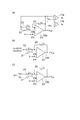
<参照電圧発生部>
図2は、図1に示された参照電圧発生部70の構成を示す回路図である。図2に示されるように、参照電圧発生部70は、A/D変換回路17に提供される第1の変換参照電圧VRCH及び第2の変換参照電圧VRCLを生成する。参照電圧発生部70は、基準電圧源33,35,36,37,38と接続される。基準電圧源33は参照電圧発生部70に第1の基準参照電圧VRHを提供する。基準電圧源35は参照電圧発生部70に第2の基準参照電圧VRLを提供する。基準電圧源36は参照電圧発生部70に電圧(VC+ΔVT)を提供する。基準電圧源37は参照電圧発生部70に電圧(VC)を提供する。基準電圧源38は参照電圧発生部70に電圧(VC−ΔVT)を提供する。また、参照電圧発生部70は、ゲインステージ15の出力15bと接続される。ゲインステージ15の出力15bは参照電圧発生部70に演算値VOPを提供する。さらに、参照電圧発生部70は、コンパレータ17aに第1の変換参照電圧VRCHを提供する。参照電圧発生部70は、コンパレータ17bに第2の変換参照電圧VRCLを提供する。
<Reference voltage generator>
FIG. 2 is a circuit diagram showing a configuration of reference
参照電圧発生部70は、第1の論理回路71と、第2の論理回路72と、第1の参照電圧発生回路73と、第2の参照電圧発生回路74と、スイッチ75,76と、を含む。第1の参照電圧発生回路73は、第1の論理回路71から提供される制御信号φHL,φML,φLLに基づいて、第1の変換参照電圧VRCHを生成する。第2の参照電圧発生回路74は、制御信号SI,SAに基づいて、第1の変換参照電圧VRCH及び第2の変換参照電圧VRCLを生成する。スイッチ75,76は、第2の論理回路72から提供される制御信号φCH1,φCH2に基づいて、第1の参照電圧発生回路73と第2の参照電圧発生回路74とを選択的にコンパレータ17aに接続する。従って、第1の参照電圧発生回路73で生成された第1の変換参照電圧VRCH及び第2の参照電圧発生回路74で生成された第1の変換参照電圧VRCHの一方がコンパレータ17aに提供される。
The reference
第1の論理回路71は、ゲインステージ15の出力15bと、基準電圧源37と、に接続される。第1の論理回路71は、基準電圧源37から提供された電圧(VC)に対する演算値VOPの大小関係を取得し、制御信号φHL,φML,φLLを生成する。第1の論理回路71は、以下のように動作する。
n=1,2であるとき、φHL=0,φML=1,φLL=0
n≧3であるとき、
VOP≧VC(n≧3):φHL=0,φML=0,φLL=1
VOP<VC(n≧3):φHL=1,φML=0,φLL=0
The
When n = 1, 2, φ HL = 0, φ ML = 1, φ LL = 0
When n ≧ 3,
V OP ≧ V C (n ≧ 3): φ HL = 0, φ ML = 0, φ LL = 1
V OP <V C (n ≧ 3): φ HL = 1, φ ML = 0, φ LL = 0
なお、制御信号φMLは、第1の論理回路71とは別の論理回路において生成されてもよい。すなわち、制御信号φMLは、演算値VOPに基づくことなく生成されてもよい。
The control signal φ ML may be generated in a logic circuit different from the
ここで、nはゲインステージ15におけるフォールディング積分動作の数を示す。例えば、n=2とは、ゲインステージ15における2回目のフォールディング積分動作であることを示す。上記の動作によれば、1回目及び2回目のフォールディング積分動作であるとき、制御信号(φHL=0,φML=1,φLL=0)により、スイッチ73bは導通とされ、スイッチ73a,73cは非導通とされる。また、3回目以降のフォールディング積分動作であって、2回目のフォールディング積分動作の結果がVC≧VOPであるとき、制御信号(φHL=0,φML=0,φLL=1)により、スイッチ73aが導通とされ、スイッチ73b,73cが非導通とされる。一方、3回目以降のフォールディング積分動作であって、2回目のフォールディング積分動作の結果がVC<VOPであるとき、制御信号(φHL=1,φML=0,φLL=0)により、スイッチ73cは導通とされ、スイッチ73a,73bは非導通とされる。
Here, n indicates the number of folding integration operations in the
なお、第1の論理回路71における比較動作は、コンパレータ17aの出力を利用して行われてもよい。この場合には、参照電圧発生部70は、A/D変換回路17と接続される。
Note that the comparison operation in the
第2の論理回路72は、制御信号φCH1,φCH2を生成する。制御信号φCH1は、スイッチ75の開閉動作を制御する。制御信号φCH2は、スイッチ76の開閉動作を制御する。第2の論理回路72は、以下のように動作する。
第1のA/D変換動作であるとき:φCH1=1,φCH2=0
第2のA/D変換動作であるとき:φCH1=0,φCH2=1
The
When the first A / D conversion operation is performed: φ CH1 = 1, φ CH2 = 0
When the second A / D conversion operation is performed: φ CH1 = 0, φ CH2 = 1
第1の参照電圧発生回路73は、第1のA/D変換動作のための第1の変換参照電圧VRCHを生成する。第1の参照電圧発生回路73には、電圧(VC,VC+ΔVT,VC−ΔVT)が提供される。第1の参照電圧発生回路73は、スイッチ73a,73b,73cを含む。スイッチ73aは、制御信号φLLにより開閉動作が制御される。スイッチ73bは、制御信号φMLにより開閉動作が制御される。スイッチ73cは、制御信号φHLにより開閉動作が制御される。第1の参照電圧発生回路73は、制御信号φHL,φML,φLLに基づき、第1の変換参照電圧VRCHとして、電圧(VC,VC+ΔVT,VC−ΔVT)のうちいずれか一つを選択的に出力する。それぞれの電圧(VC)及び電圧(ΔVT)は、下記式(1A),(1B),(1C)により示される。
ここで、式(1B)におけるdは、演算値VOPと演算値VOPの上限値との間の余裕、及び、演算値VOPと演算値VOPの下限値との間の余裕を設定する値であり、0<d<1の範囲における所定の数値に設定される。例えば、d=0.25とされる。
The first reference
Here, d in Formula (1B), a margin between the operation value V OP and the upper limit value of the operation value V OP, and sets the margin between the operation value V OP and the lower limit value of the operation value V OP And is set to a predetermined numerical value in the range of 0 <d <1. For example, d = 0.25.
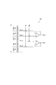
図3は、図2に示された第2の参照電圧発生回路74の構成を示す回路図である。図3に示されるように、第2の参照電圧発生回路74は、第2のA/D変換動作のための第1の変換参照電圧VRCH及び第2の変換参照電圧VRCLを生成する。第2の参照電圧発生回路74は、第1の基準参照電圧VRH及び第2の基準参照電圧VRLに基づき、第1の変換参照電圧VRCH及び第2の変換参照電圧VRCLを生成する。第1の基準参照電圧VRH及び第2の基準参照電圧VRLは、基準電圧源33,35から提供される。第2の参照電圧発生回路74は、第1の基準参照電圧VRH及び第2の基準参照電圧VRLに基づき、所定の抵抗値を有する抵抗R1〜R5に応じて、電圧(VRC1H,VRC2H,VRC2L,VRC1L)を生成する。第2のA/D変換動作では、制御信号SAによって制御されるスイッチの動作により、第1の変換参照電圧VRCHとして電圧(VRC2H)が提供され、第2の変換参照電圧VRCLとして電圧(VRC2L)が提供される。
FIG. 3 is a circuit diagram showing a configuration of second reference
この第2の参照電圧発生回路74によれば、第1の変換参照電圧VRCHは、第1の基準参照電圧VRHと第2の基準参照電圧VRLとの間の中央値より高く且つ第1の基準参照電圧VRHより低い。また、第2の変換参照電圧VRCLは、第1の基準参照電圧VRHと第2の基準参照電圧VRLとの間の中央値より低く且つ第2の基準参照電圧VRLより高い。このように第1の変換参照電圧VRCH及び第2の変換参照電圧VRCLが生成されるので、第1のA/D変換動作及び第2のA/D変換動作が適切に実施される。
According to the second reference
例えば、抵抗R1,R2,R3,R4,R5の抵抗値を、抵抗R1=2R、抵抗R2=R、抵抗R3=2R、抵抗R4=R、抵抗R5=2R(Rは所定の抵抗値)といった値に設定することにより、第2のA/D変換動作における第1の変換参照電圧VRCH及び第2の変換参照電圧VRCLとして、以下の式により表される電圧(VRC2H,VRC2L)が提供される。
VRC2H=(5VRH+3VRL)/8
VRC2L=(3VRH+5VRL)/8
このように第1の変換参照電圧VRCH及び第2の変換参照電圧VRCLが生成されるので、より適切に第2のA/D変換動作が実施される。
For example, the resistance values of the resistors R1, R2, R3, R4, and R5 are the resistor R1 = 2R, the resistor R2 = R, the resistor R3 = 2R, the resistor R4 = R, and the resistor R5 = 2R (R is a predetermined resistance value). By setting the values, the voltages (V RC2H , V RC2L ) represented by the following expressions are used as the first conversion reference voltage V RCH and the second conversion reference voltage V RCL in the second A / D conversion operation. Is provided.
V RC2H = (5V RH + 3V RL ) / 8
V RC2L = (3V RH + 5V RL ) / 8
Since the first conversion reference voltage V RCH and the second conversion reference voltage V RCL are generated in this way, the second A / D conversion operation is more appropriately performed.
再び図1に示されるように、論理回路19は、ディジタル値Dに応じた制御信号VCONT(例えばφDH、φDL、φDS)を生成する。
As shown in FIG. 1 again, the
D/A変換回路21は、第1の出力21aと、第2の出力21bとを含む。D/A変換回路21は、第1の基準参照電圧VRH及び第2の基準参照電圧VRLの少なくともいずれか一方を、制御信号VCONTに応じて第1の出力21a及び第2の出力21bを介してゲインステージ15に提供する。第1の基準参照電圧VRH及び第2の基準参照電圧VRLは、基準電圧源33,35から提供される。
The D /
D/A変換回路21は、制御信号に応じて動作するスイッチ回路31を含む。スイッチ回路31は、第1の基準参照電圧VRH及び第2の基準参照電圧VRLのいずれかを、D/A変換回路21が第1の出力21aに提供するように動作する。スイッチ回路31は、第1の基準参照電圧VRH及び第2の基準参照電圧VRLのいずれかを、D/A変換回路21が第2の出力21bに提供するように動作する。
The D /
スイッチ回路31は、スイッチ31a,31b,31cを含む。スイッチ回路31は、スイッチ31a,31bを動作させることにより、第1の基準参照電圧VRHを第1の出力21aに提供すると共に、第2の基準参照電圧VRLを第2の出力21bに提供する。また、スイッチ回路31は、スイッチ31a,31cを動作させることにより、第1の基準参照電圧VRHを第1の出力21a及び第2の21bに提供する。さらに、スイッチ回路31は、スイッチ31b,31cを動作させることにより、第2の基準参照電圧VRLを第1の出力21a及び第2の21bに提供する。
The
D/A変換回路21の第1の出力21aは、第1のキャパシタ25の一端に接続される。D/A変換回路21の第2の出力21bは、第2のキャパシタ27の一端に接続される。スイッチ31a,31b,31cの開閉は、それぞれ、論理回路19からの制御信号φDH,φDS,φDLによって制御される。従って、ディジタル値Dは、動作させるべき制御信号φDH,φDS,φDLを決定する。
The
ここで、第1の出力21aに提供される電圧をVDA1とし、第2の出力21bに提供される電圧をVDA2とする。そして、A/D変換回路17が1つのコンパレータ17aを用いてディジタル値Dを生成する場合には、D/A変換回路21は、A/D変換回路17からのディジタル値Dに基づく制御信号VCONTに応じて、以下のように動作する。
条件(D=1)が満たされるとき:VDA1=VRH、VDA2=VRL
条件(D=0)が満たされるとき:VDA1=VDA2=VRL
Here, it is assumed that the voltage provided to the
When condition (D = 1) is satisfied: V DA1 = V RH , V DA2 = V RL
When condition (D = 0) is satisfied: V DA1 = V DA2 = V RL
一方、A/D変換回路17が2つのコンパレータ17a,17bを用いてディジタル値Dを生成する場合には、D/A変換回路21は、A/D変換回路17からのディジタル値Dに基づく制御信号VCONTに応じて、以下のように動作する。
条件(D=2)が満たされるとき:VDA1=VDA2=VRH
条件(D=1)が満たされるとき:VDA1=VRH、VDA2=VRL
条件(D=0)が満たされるとき:VDA1=VDA2=VRL
On the other hand, when the A /
When condition (D = 2) is satisfied: V DA1 = V DA2 = V RH
When condition (D = 1) is satisfied: V DA1 = V RH , V DA2 = V RL
When condition (D = 0) is satisfied: V DA1 = V DA2 = V RL
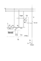
本発明の別の側面は、イメージセンサデバイスである。図4は、イメージセンサの画素を示す図面である。イメージセンサデバイスは、セルアレイと、変換器アレイとを備える。セルアレイは、二次元状に配置された複数のイメージセンサセル2aを含む。変換器アレイは、セルアレイに接続されており複数のA/D変換器11を含む。A/D変換器11は、セルアレイのカラム線8を介してイメージセンサセル2aに接続される。
Another aspect of the present invention is an image sensor device. FIG. 4 is a diagram illustrating pixels of the image sensor. The image sensor device includes a cell array and a transducer array. The cell array includes a plurality of
イメージセンサセル2aは、例えばCMOSイメージセンサセルである。フォトダイオードDFは、イメージに関連する一画素分の光Lを受ける。選択トランジスタMSのゲートは、行方向に伸びるロウ選択線Sに接続される。リセットトランジスタMRのゲートはリセット線Rに接続される。転送トランジスタMTのゲートは、行方向に伸びる転送選択線に接続される。フォトダイオードDFの一端は転送トランジスタMTを介して浮遊拡散層FDに接続される。浮遊拡散層FDは、リセットトランジスタMRを介してリセット電位線Resetに接続されると共に、トランジスタMAのゲートに接続される。トランジスタMAの一電流端子(例えばドレイン)は、選択トランジスタMSを介してカラム線8に接続される。トランジスタMAは、浮遊拡散層FDの電荷量に応じて電位を選択トランジスタMSを介してカラム線に提供する。
The
この構造のイメージセンサセル2aは、リセットレベルを示す第1の信号と該リセットレベルに重畳された信号レベルを示す第2の信号とを生成する。すなわち、イメージセンサセル2aでは、まず、リセット線Rに提供される制御信号がリセットトランジスタMRに提供され、浮遊拡散層FDがリセットされる。トランジスタMAを介して、このリセットレベルが読み出される。次に、電荷転送制御信号TXが転送トランジスタMTに提供され、フォトダイオードDFから光誘起信号電荷が浮遊拡散層に転送される。そして、トランジスタMAを介して、この信号レベルが読み出される。このように、イメージセンサセル2aは、リセットレベルを示す第1の信号S1と該リセットレベルに重畳された信号レベルを示す第2の信号S2とを生成可能である。
The
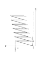
<フォールディング積分型A/D変換動作>
次に、図1に示されたA/D変換器11における第1のA/D変換動作を説明する。第1のA/D変換動作は、入力信号の標本化及び標本値の積分を繰り返し行うことによりアナログ値である入力値VINからディジタル値Dである出力値を得るためのフォールディング積分型の動作である。
<Folding integration type A / D conversion operation>
Next, the first A / D conversion operation in the A /
図5の(a)部、(b)部、(c)部及び(d)部は、第1のA/D変換動作を説明するための回路図である。第1のA/D変換動作では、前述したように、A/D変換回路17が1つのコンパレータ17aを用いてディジタル値Dを生成する。
Parts (a), (b), (c) and (d) of FIG. 5 are circuit diagrams for explaining the first A / D conversion operation. In the first A / D conversion operation, as described above, the A /
図5の(a)部に示されるように、ゲインステージ15は、第1の初期格納ステップとしての第1の格納動作を行う。このステップでは、ゲインステージ15の入力15aを介して受けた入力値VINを第1のキャパシタ25に格納する。また、ゲインステージ15の出力23bと第1の入力23aとを接続する。そして、第2のキャパシタ27は、第2の出力21bから提供される第2の基準参照電圧VRLを格納する。さらに、第3のキャパシタ29は、演算増幅回路23の出力23bと第1の入力23aとの間に接続される。
As shown in part (a) of FIG. 5, the
第1の初期格納ステップ及び以下に説明する各ステップにおける格納及び接続は、スイッチ回路31及びスイッチ43,47,49,51,53により実現される。第1の初期格納ステップでは、制御信号(φDH=0,φDS=0,φDL=1)及び制御信号(φ1=1,φ2=0,φ3=0,φR=1,φS=1)により、スイッチ31b,47,53,43は導通とされ、スイッチ31a,31c,49,51は非導通とされる。
Storage and connection in the first initial storage step and each step described below are realized by the
このとき、容量C1a,C1bに蓄積される電荷(Q1a,Q1b)は、下記式(2A),(2B)により示される。
第1の初期格納動作ステップに引き続き、A/D変換器11は、図5の(b)部又は図5の(c)部に示される、第1の演算ステップとしての第1の演算動作を行う。
Subsequent to the first initial storage operation step, the A /
第1の演算ステップでは、制御信号(φ1=0,φ2=1,φ3=0,φR=0,φS=0)により、スイッチ49は導通とされ、スイッチ47,51,53,43は非導通とされる。この回路構成によれば、第1のキャパシタ25が第1の出力21aと第1の入力23aとの間に接続され、第2のキャパシタ27が第2の出力21bと第1の入力23aとの間に接続され、第3のキャパシタ29が演算増幅回路23の出力23bと第1の入力23aとの間に接続される。
In the first calculation step, the
D/A変換回路21の第1の出力21a及び第2の出力21bには、コンパレータ17aからのディジタル値D(n)(=B1)に従ったスイッチ回路31の制御により、第1の基準参照電圧VRH又は第2の基準参照電圧VRLが提供される。
The
1回目及び2回目の第1の演算動作が行われるとき、参照電圧発生部70は、第1の変換参照電圧VRCHとして第1の閾値をA/D変換回路17に提供する。この場合、参照電圧発生部70では、制御信号(φHL=0,φML=1,φLL=0,φCH1=1,φCH2=0)により、スイッチ73b,75は導通とされ、スイッチ73a,73c,76は非導通とされる。
When the first and second first calculation operations are performed, the reference
ここで、参照電圧発生部70は、2回目の第1の演算動作の結果を利用して、制御値Eである第1の制御値または第2の制御値を生成する。制御値Eは、3回目以降の第1の演算動作に利用される閾値である第1の変換参照電圧VRCHを生成するための値である。この動作は、参照電圧発生部70の第1の論理回路71において行われる。第1の論理回路71は、以下のように動作する。VOP(2)は、2回目の第1の演算動作により生成された演算値である。
条件(VOP(2)≧VC)が満たされるとき、E=1
条件(VOP(2)<VC)が満たされるとき、E=0
Here, the reference
When the condition (V OP (2) ≧ V C ) is satisfied, E = 1
E = 0 when the condition (V OP (2) <V C ) is satisfied
具体的には、演算値VOP(2)が第1の閾値(VC)以上であるとき、制御値Eは第1の制御値(E=1)である。一方、演算値VOP(2)が第1の閾値(VC)未満であるとき、制御値Eは第2の制御値(E=0)である。なお、この制御値は、2回目の第1の演算動作の結果(演算値VOP(2))に基づくコンパレータ17aのディジタル出力(D(2)=0又は1)を利用してもよい。
Specifically, when the calculated value V OP (2) is greater than or equal to the first threshold value (V C ), the control value E is the first control value (E = 1). On the other hand, when the calculated value V OP (2) is less than the first threshold value (V C ), the control value E is the second control value (E = 0). As this control value, the digital output (D (2) = 0 or 1) of the
1回目及び2回目の第1の演算動作が行われるとき、A/D変換回路17のコンパレータ17aは、式(3)に示されるように動作する。式(3)において、D(n)=(B1)はn回目の演算動作おけるディジタル値Dが(B1)であることを示す。nはゲインステージ15におけるフォールディング積分動作の数を示す。例えば、D(1)=1は1回目のフォールディング演算動作におけるディジタル値Dが「1」であることを示す。
3回目以降の第1の演算動作が行われるとき、参照電圧発生部70及びA/D変換回路17のコンパレータ17aは、式(4)に示されるように動作する。ただし、3≦n<Mである。Mは、最大繰り返し数(積分の回数)である。
式(4)によれば、参照電圧発生部70は、第1の変換参照電圧VRCHとして電圧[VC−d×ΔVR×(2×E−1)]をA/D変換回路17に提供する。そして、A/D変換回路17は、演算値VOP(n)(3≦n<M)に基づき、第1の変換参照電圧VRCHを参照して、ディジタル値Dを生成する。
According to Expression (4), the reference
式(4)において、[VC−d×ΔVR×(2×E−1)]は、コンパレータ17aに提供される第2の閾値又は第3の閾値である。制御値Eは、第2の閾値又は第3の閾値を決定する。第2の閾値又は第3の閾値を示す数式[VC−d×ΔVR×(2×E−1)]を参照すると、制御値Eが含まれている。制御値Eは、2回目の第1の演算動作の結果に基づいて生成される値である。すなわち、3回目以降の演算動作においては、2回目の演算動作で得られた結果(制御値E)を用いて閾値(第1の変換参照電圧VRCH)を決定している。既に述べたように、式(4)におけるdは、演算値VOPと演算値VOPの上限値との間の余裕、及び、演算値VOPと演算値VOPの下限値との間の余裕を設定する値であり、0<d<1の範囲における所定の数値に設定される。例えば、d=0.25とされる。
In Expression (4), [V C −d × ΔV R × (2 × E−1)] is a second threshold value or a third threshold value provided to the
例えば、第1の制御値(E=1)であるとき、第1の制御値(E=1)を式(4)に代入すると、式(5)に示される第2の閾値(VC−d×ΔVR)が得られる。第2の閾値は、第1の閾値VCより[d×ΔVR]だけ小さい。この場合、参照電圧発生部70では、制御信号(φHL=0,φML=0,φLL=1,φCH1=1,φCH2=0)により、スイッチ73a,75が導通とされ、スイッチ73b,73c,76が非導通とされる。
一方、第2の制御値(E=0)であるとき、第2の制御値(E=0)を式(4)に代入すると、式(6)に示される第3の閾値(VC+d×ΔVR)が得られる。第3の閾値は、第1の閾値VCより[d×ΔVR]だけ大きい。この場合、参照電圧発生部70では、制御信号(φHL=1,φML=0,φLL=0,φCH1=1,φCH2=0)により、スイッチ73c,75が導通とされ、スイッチ73a,73b,76が非導通とされる。
要するに、1回目及び2回目の演算動作では、第1の変換参照電圧VRCHとして電圧(VC)がコンパレータ17aに提供される。そして、2回目の演算動作の結果に基づいて第1の制御値(E=1)が生成された場合には、第1の変換参照電圧VRCHとして電圧(VC−d×ΔVR)がコンパレータ17aに提供される。一方、2回目の演算動作の結果に基づいて、第2の制御値(E=2)が生成された場合には、第1の変換参照電圧VRCHとして電圧(VC+d×ΔVR)がコンパレータ17aに提供される。
In short, in the first and second calculation operations, the voltage (V C ) is provided to the
続いて、ゲインステージ15は、図5(d)に示される第1の格納動作を第1の格納ステップとして行う。第1の格納ステップでは、第3のキャパシタ29を演算増幅回路23の出力23bと第1の入力23aとの間に接続することで演算値VOPを容量C2に保持したままで、ゲインステージ15の入力15aからの入力値VINを第1のキャパシタ25に格納し、第2の出力21bから提供される第2の基準参照電圧VRLを第2のキャパシタ27に格納する。第1の格納ステップでは、制御信号(φDH=0,φDS=0、φDL=1)及び制御信号(φ1=1,φ2=0,φ3=0,φR=0,φS=1)により、スイッチ31b,47,43は導通とされ、スイッチ31a,31c,49,51,53は非導通とされる。
Subsequently, the
次いで、ゲインステージ15は、ディジタル値D(n−1)に基づき、図5の(b)部及び図5の(c)部に示される第1の演算動作のいずれかを選択しながら、n回目の第1の演算ステップ及び第1の格納ステップを行うフォールディング積分型A/D変換ステップを所定回数繰り返して実施する。フォールディング積分型A/D変換ステップにおいて、第1の演算ステップ及び第1の格納ステップをM回繰り返して、サンプリング及び積分を行ったときの演算値VOPは、式(7A),(7B)により示される。式(7A)において、ディジタル値D(n)は、上記式(5)又は式(6)により示される。
式(7A)の右辺第2項に示されるように、入力信号である入力値VINに1/2のゲインをかけて、M回のサンプリングを行い、フォールディング積分型のA/D変換を行うと、その出力(演算値VOP)の振幅範囲は、入力信号の振幅範囲と同じになる。 As shown in the second term on the right side of Expression (7A), the input value VIN , which is an input signal, is multiplied by a half gain, sampling is performed M times, and folding integration type A / D conversion is performed. The amplitude range of the output (calculated value V OP ) is the same as the amplitude range of the input signal.
<巡回型A/D変換動作>
次に、図1に示されたA/D変換器11における第2のA/D変換動作を説明する。第2のA/D変換動作は、巡回型A/D変換動作である。以下、A/D変換器11における、巡回型A/D変換ステップとしての巡回型A/D変換の動作を説明する。
<Circular A / D conversion operation>
Next, the second A / D conversion operation in the A /
図6の(a)部、(b)部及び(c)部は、第2のA/D変換動作を説明するための回路図である。第2のA/D変換動作では、A/D変換回路17が2つのコンパレータ17a,17bを用いてディジタル値Dを生成する。
Parts (a), (b), and (c) of FIG. 6 are circuit diagrams for explaining a second A / D conversion operation. In the second A / D conversion operation, the A /
まず、ゲインステージ15は、図6の(a)部に示されるように、第2の初期格納ステップとしての第2の格納動作を実施する。このステップでは、フォールディング積分型A/D変換ステップにおける演算値VOPである残差アナログ信号を第1のキャパシタ25、第2のキャパシタ27及び第3のキャパシタ29に格納する。このステップでは、制御信号(φDH=0,φDS=1、φDL=0)及び制御信号(φ1=1,φ2=0,φ3=1,φR=0,φS=0)により、スイッチ31c,47,51は導通とされ、スイッチ31a,31b,43,49,53は非導通とされる。また、このステップでは、フォールディング積分型A/D変換ステップにおける演算値VOPがコンパレータ17a,17bに提供される。コンパレータ17a,17bは、提供された演算値VOPに基づき、ディジタル値Dを生成する。
First, as shown in FIG. 6A, the
続いて、ゲインステージ15は、第2の初期格納ステップに引き続き、ディジタル値D(=B1+B0)の値に従って、図6の(b)部又は図6の(c)部に示されるように、第2の演算ステップとしての第2の演算動作を行う。第2の演算動作では、ゲインステージ15は、演算増幅回路23、第1のキャパシタ25、第2のキャパシタ27及び第3のキャパシタ29により演算値VOPを生成する。第2の演算動作では、第3のキャパシタ29が演算増幅回路23の出力23bと第1の入力23aとの間に接続されると共に、第1のキャパシタ25が第1の出力21aと第1の入力23aとの間に接続され、第2のキャパシタ27が第2の出力21bと第1の入力23aとの間に接続される。第2の演算ステップでは、制御信号(φ1=0,φ2=1,φ3=0,φR=0,φS=0)により、スイッチ49は導通とされ、スイッチ47,51,53,43は非導通とされる。
Subsequently, following the second initial storage step, the
D/A変換回路21の第1の出力21a及び第2の出力21bには、コンパレータ17a,17bからのディジタル値D(=B1+B0)に従ってスイッチ回路31が制御され、第1の基準参照電圧VRH又は第2の基準参照電圧VRLが提供される。
The
コンパレータ17a,17bは、以下のように動作する。
VOP>VRCHのとき D=2(B1=1,B0=1)
VRCL<VOP≦VRCHのとき D=1(B1=0,B0=1)
VOP≦VRCLのとき D=0(B1=0,B0=0)
The
When V OP > V RCH D = 2 (B 1 = 1, B 0 = 1)
When V RCL <V OP ≦ V RCH D = 1 (B 1 = 0, B 0 = 1)
When V OP ≦ V RCL D = 0 (B 1 = 0, B 0 = 0)
D=2のときには、D/A変換回路21の第1の出力21a及び第2の出力21bから第1の基準参照電圧VRHが提供されるように制御されながら図6の(b)部の動作が行われる。一方、D=0のときには、D/A変換回路21の第1の出力21a及び第2の出力21bから第2の基準参照電圧VRLが提供されるように制御されながら図6の(b)部の動作が行われる。さらに、D=1のときには、D/A変換回路21の第1の出力21a及び第2の出力21bからそれぞれ第1の基準参照電圧VRH及び第2の基準参照電圧VRLが提供されるように制御されながら図6の(c)部の動作が行われる。
When D = 2, the first reference reference voltage VRH is controlled so as to be provided from the
続いて、ゲインステージ15は、第2の演算ステップに引き続き、図6の(a)部に示されるように、第2の格納ステップとしての第2の格納動作を行う。
Subsequently, following the second calculation step, the
第2の格納ステップでは、第2の演算ステップにおける演算値VOPを第1のキャパシタ25、第2のキャパシタ27及び第3のキャパシタ29に格納する点において、第2の初期格納ステップと相違する。
The second storing step is different from the second initial storing step in that the calculated value V OP in the second calculating step is stored in the
そして、ゲインステージ15は、巡回型A/D変換ステップとして、第2の演算ステップ及び第2の格納ステップを所定回数繰り返して行う。M回の積分動作後の演算値VOP(M)の残差に対するj回目の巡回動作後に得られるディジタル値をD(j)で表すと、残差VOP(M)−VCOMとディジタル値D(j)の関係は式(8)により示される。
式(7A)のD(M)と、式(8)のD(1)〜D(N)より、アナログ値である入力値からディジタル値である出力値が得られる。
Then, the
From D (M) in Expression (7A) and D (1) to D (N) in Expression (8), an output value that is a digital value is obtained from an input value that is an analog value.
以下、本実施形態に係るA/D変換器11の作用効果について説明する。
Hereinafter, the effect of the A /
このA/D変換器11では、ゲインステージ15の出力15bから送出される演算値VOPに基づいて第1の変換参照電圧VRCHを生成する。そして、第1の変換参照電圧VRCHを参照して、ゲインステージ15からの演算値VOPがディジタル値Dに変換される。これにより、第1の変換参照電圧VRCHは、唯一の値ではなく可変値であるので、積分動作の繰り返しによってもゲインステージ15の出力15bから送出される演算値VOPが所望の範囲を超えないようにすることが可能になる。従って、このA/D変換器11は、積分演算の結果を所望の範囲に収めることができる。
The A /
このゲインステージ15では、第3のキャパシタ29の容量C2が、第1のキャパシタ25の容量C1a及び第2のキャパシタ27の容量C1bに対して2倍である。換言すると、第1のキャパシタ25及び第2のキャパシタ27と、第3のキャパシタ29との容量比が1/2である。従って、演算増幅回路23における電圧の出力範囲は、入力範囲の1/2になる。このため、このゲインステージ15によれば、1回目の積分動作によって入力信号の大きさが1/2となる。次に、2回目の積分動作では1回目の積分動作の結果と、1/2とされる演算増幅回路23の演算値VOPとが足し合される。従って、2回目の積分動作の出力の大きさは、入力値VINの大きさに対応する。これにより、第1の変換参照電圧VRCHの生成において、2回目の積分動作の出力を参照することは、入力を参照することと同じ意味である。従って、ゲインステージ15の演算値VOPを利用して、積分演算の結果を所望の範囲に収めることが可能な第1の変換参照電圧VRCHを生成することができる。
In the
図7及び図8を参照しつつ、参照電圧発生部70の作用につきさらに説明する。図7及び図8は、ゲインステージ15のフォールディング積分型A/D変換器としての動作時における入出力特性を概略的に示す図である。参照電圧発生部70は、2回目の積分動作で得られたゲインステージ15の出力に基づいて、第1の制御値又は第2の制御値を生成する。そして、参照電圧発生部70は、3回目の積分動作で得られたゲインステージ15の出力をA/D変換するための第1の変換参照電圧VRCHを、第2の閾値(VC−ΔVT)又は第3の閾値(VC+ΔVT)に基づいて生成する。そして、第1の閾値(VC)及び第1の制御値に基づいて生成された第2の閾値(VC−ΔVT)は、第1の閾値(VC)より小さい。一方、第1の閾値(VC)及び第2の制御値に基づいて生成された第3の閾値(VC+ΔVT)は、第1の閾値(VC)より大きい。その結果、ゲインステージ15の出力が大きい場合には閾値が小さくなり、ゲインステージ15の出力が小さい場合には閾値が大きくなる。
The operation of the
ここで、閾値は、ゲインステージ15の出力を所定の範囲に収めるために、演算値VOPから所定の値(ΔVR)を減じる動作(いわゆる折り返し動作)を行うか否かを判断するための値である。そうすると、第2の閾値が第1の閾値(VC)より小さい場合(VC−ΔVT)には、ゲインステージ15の出力が小さい段階で折り返し動作が実行されることになる(図7参照)。従って、ゲインステージ15の出力から上限値(Vmax)までの間の余裕をΔVm1からΔVm2へ拡大させることが可能になる。また、第3の閾値が第1の閾値(VC)より大きい場合(VC+ΔVT)には、ゲインステージ15の出力が大きい段階で折り返し動作が実行されることになる(図8参照)。従って、ゲインステージ15の出力から下限値(Vmin)までの間の余裕をΔVm3からΔVm4へ拡大させることが可能になる。
Here, the threshold value is used to determine whether or not to perform an operation of reducing a predetermined value (ΔV R ) from the calculated value V OP (so-called folding operation) in order to keep the output of the
このA/D変換器11では、コンパレータ17aの比較動作における誤差耐性を高めることが可能になる。従って、精密な参照電圧を提供するために高精度の電源を用いる必要がなくなる。
In the A /
また、第1の閾値(VC)は、第1の基準参照電圧VRHと、第2の基準参照電圧VRLとの中間値である(式(1A)参照)。この構成によれば、ゲインステージ15に入力される入力値VINの許容範囲において、第1の閾値(VC)よりも小さい第2の閾値(VC−ΔVT)を用いてA/D変換される範囲と、第1の閾値(VC)よりも大きい第2の閾値(VC+ΔVT)を用いてA/D変換される範囲と、の境界を、当該許容範囲の中間に設定することができる。
The first threshold value (V C ) is an intermediate value between the first standard reference voltage V RH and the second standard reference voltage V RL (see Expression (1A)). According to this configuration, in the allowable range of the input value VIN input to the
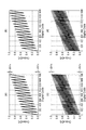
<比較例1>
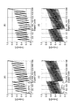
図9の(a)部〜(d)部は、シミュレーションにより求めたゲインステージのフォールディング積分型A/D変換器としての動作時における入出力特性を示す図面である。縦軸は、A/D変換前の入力値VIN(アナログ値)であり、横軸は、入力値VINをA/D変換後の値(14ビットディジタル値)である。すなわち、横軸は、入力値VIN(ディジタル値)であり、14ビットでA/D変換した結果出力されると期待されるディジタル値に換算して示している。図9の(a)部〜(d)部に示される入出力特性は、比較例に係る参照電圧発生部から提供される基準参照電圧に基づいている。比較例に係る参照電圧発生部は、基準参照電圧を生成するための閾値が一定値(第1の閾値(VC))として動作する。また、シミュレーションのための条件として、(VC=0.5V、VRH=1.0V、VRL=0V、VCOM=0V)が設定された。
<Comparative Example 1>
Parts (a) to (d) of FIG. 9 are diagrams showing input / output characteristics when the gain stage is operated as a folding integral type A / D converter obtained by simulation. The vertical axis represents the input value V IN (analog value) before A / D conversion, and the horizontal axis represents the value (14-bit digital value) after A / D conversion of the input value VIN . That is, the horizontal axis represents the input value V IN (digital value), which is converted into a digital value expected to be output as a result of A / D conversion with 14 bits. The input / output characteristics shown in the parts (a) to (d) of FIG. 9 are based on the reference reference voltage provided from the reference voltage generating part according to the comparative example. The reference voltage generation unit according to the comparative example operates with a threshold for generating the reference reference voltage as a constant value (first threshold (V C )). Further, (V C = 0.5 V, V RH = 1.0 V, V RL = 0 V, V COM = 0 V) were set as conditions for the simulation.
図9の(a)部及び図9の(b)部は、積分回数(M=16)とした場合のシミュレーション結果である。また、図9の(a)部は、理想的なフォールディング積分型A/D変換回路として、コンパレータの電圧バイアス等の誤差要因を含んでいない。一方、図9の(b)部は、実際のフォールディング積分型A/D変換回路として、コンパレータの電圧バイアス等の誤差要因を含む。図9の(a)部に示された入出力特性によれば、上限値(又は下限値)までの余裕(ΔVm)は、0.036Vであることがわかった。従って、図9の(b)部に示されるように、電圧バイアス等の誤差に対して0.036Vの余裕があることがわかった。 Part (a) of FIG. 9 and part (b) of FIG. 9 are the simulation results when the number of integrations (M = 16). Further, the part (a) of FIG. 9 does not include an error factor such as a voltage bias of a comparator as an ideal folding integration type A / D conversion circuit. On the other hand, part (b) of FIG. 9 includes an error factor such as a voltage bias of a comparator as an actual folding integration type A / D conversion circuit. According to the input / output characteristics shown in part (a) of FIG. 9, it was found that the margin (ΔV m ) up to the upper limit (or lower limit) was 0.036V. Therefore, as shown in part (b) of FIG. 9, it was found that there was a margin of 0.036V for errors such as voltage bias.
図9の(c)部及び図9の(d)部は、積分回数(M=64)とした場合のシミュレーション結果である。また、図9の(c)部は、理想的なフォールディング積分型A/D変換回路として、コンパレータの電圧バイアス等の誤差要因を含んでいない。一方、図9の(d)部は、実際のフォールディング積分型A/D変換回路として、コンパレータの電圧バイアス等の誤差要因を含む。図9の(c)部に示された入出力特性によれば、上限値(又は下限値)までの余裕(ΔVm)は、0.0077Vであることがわかった。従って、図9の(d)部に示されるように、電圧バイアス等の誤差に対して0.0077Vの余裕があることがわかった。 Part (c) of FIG. 9 and part (d) of FIG. 9 are the simulation results when the number of integrations (M = 64). 9C does not include an error factor such as a voltage bias of a comparator as an ideal folding integration type A / D conversion circuit. On the other hand, part (d) of FIG. 9 includes an error factor such as a voltage bias of a comparator as an actual folding integration type A / D conversion circuit. According to the input / output characteristics shown in part (c) of FIG. 9, the margin (ΔV m ) up to the upper limit (or lower limit) was found to be 0.0077V. Therefore, as shown in FIG. 9D, it was found that there was a margin of 0.0077V for errors such as voltage bias.
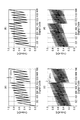
<実施例1>
図10の(a)部〜(d)部は、シミュレーションにより求めたゲインステージ15のフォールディング積分型A/D変換器としての動作時における入出力特性を示す図面である。縦軸は、A/D変換前の入力値VIN(アナログ値)であり、横軸は、入力値VINをA/D変換後の値(14ビットディジタル値)である。図10の(a)部〜(d)部に示される入出力特性は、参照電圧発生部70から提供される基準参照電圧に基づいている。また、シミュレーションのための条件として、(VC=0.5V、ΔVT=0.125V、VRH=1.0V、VRL=0V、VCOM=0V)が設定された。
<Example 1>
Parts (a) to (d) of FIG. 10 are diagrams showing input / output characteristics when the
図10の(a)部及び図10の(b)部は、積分回数(M=16)とした場合のシミュレーション結果である。また、図10の(a)部は、理想的なフォールディング積分型A/D変換回路として、コンパレータの電圧バイアス等の誤差要因を含んでいない。一方、図10の(b)部は、実際のフォールディング積分型A/D変換回路として、コンパレータ17aの電圧バイアス等の誤差要因を含む。図10の(a)部に示された入出力特性によれば、上限値(又は下限値)までの余裕(ΔVm)は、0.125Vであることがわかった。従って、図10の(b)部に示されるように、電圧バイアス等の誤差に対して0.125Vの余裕があることがわかった。また、比較例の余裕(0.036V)と比較すると、誤差耐性は3倍程度(0.125/0.036)向上することがわかった。
Part (a) of FIG. 10 and part (b) of FIG. 10 are simulation results when the number of integrations (M = 16). Further, the part (a) of FIG. 10 does not include an error factor such as a voltage bias of a comparator as an ideal folding integration type A / D conversion circuit. On the other hand, part (b) of FIG. 10 includes an error factor such as a voltage bias of the
図10の(c)部及び図10の(d)部は、積分回数(M=64)とした場合のシミュレーション結果である。また、図10の(c)部は、理想的なフォールディング積分型A/D変換回路として、コンパレータの電圧バイアス等の誤差要因を含んでいない。一方、図10の(d)部は、実際のフォールディング積分型A/D変換回路として、コンパレータ17aの電圧バイアス等の誤差要因を含む。図10の(c)部に示された入出力特性によれば、上限値(又は下限値)までの余裕(ΔVm)は、0.125Vであることがわかった。従って、図10の(d)部に示されるように、電圧バイアス等の誤差に対して0.125Vの余裕があることがわかった。また、比較例の余裕(0.0077V)と比較すると、誤差耐性は16倍程度(0.125/0.0077)向上することがわかった。
Part (c) of FIG. 10 and part (d) of FIG. 10 are simulation results when the number of integrations is set to M (64). Further, part (c) of FIG. 10 does not include an error factor such as a voltage bias of a comparator as an ideal folding integration type A / D conversion circuit. On the other hand, part (d) of FIG. 10 includes an error factor such as a voltage bias of the
<実施例2>
図11の(a)部〜(d)部は、シミュレーションにより求めたゲインステージ15のフォールディング積分型A/D変換器としての動作時における入出力特性を示す図面である。縦軸は、A/D変換前の入力値VIN(アナログ値)であり、横軸は、入力値VINをA/D変換後の値(14ビットディジタル値)である。図11の(a)部〜(d)部に示される入出力特性は、参照電圧発生部70から提供される基準参照電圧に基づいている。また、シミュレーションのための条件として、(VC=0.375V、ΔVT=0.125V、VRH=1.0V、VRL=0V、VCOM=0V)が設定された。
<Example 2>
Parts (a) to (d) of FIG. 11 are diagrams showing input / output characteristics when the
さらに、実施例2では、2回目の演算値VOPをディジタル値Dに変換するための第1の閾値として、第1の閾値(VC+ΔVR/4)を設定した。ΔVRは、上記式(1C)に示される。即ち、第1の閾値は、第1の基準参照電圧VRHと、第2の基準参照電圧VRLとの中間値(VC)よりも小さく、第2の基準参照電圧よりも大きい。 Further, in the second embodiment, the first threshold value (V C + ΔV R / 4) is set as the first threshold value for converting the second calculation value V OP into the digital value D. [Delta] V R is represented by the formula (1C). In other words, the first threshold value is smaller than the intermediate value (V C ) between the first standard reference voltage V RH and the second standard reference voltage V RL and larger than the second standard reference voltage.
図11の(a)部及び図11の(b)部は、積分回数(M=16)とした場合のシミュレーション結果である。また、図11の(a)部は、理想的なフォールディング積分型A/D変換回路として、コンパレータの電圧バイアス等の誤差要因を含んでいない。一方、図11の(b)部は、実際のフォールディング積分型A/D変換回路として、コンパレータ17aの電圧バイアス等の誤差要因を含む。図11の(a)部に示された入出力特性によれば、下限値までの余裕(ΔVm)は、0.09Vであることがわかった。従って、図11の(b)部に示されるように、電圧バイアス等の誤差に対して0.09Vの余裕があることがわかった。また、比較例の余裕(0.036V)と比較すると、誤差耐性は2.5倍程度(0.09/0.036)向上することがわかった。
Part (a) of FIG. 11 and part (b) of FIG. 11 are simulation results when the number of integrations (M = 16). 11A does not include an error factor such as a voltage bias of a comparator as an ideal folding integration type A / D conversion circuit. On the other hand, part (b) of FIG. 11 includes an error factor such as a voltage bias of the
図11の(c)部及び図11の(d)部は、積分回数(M=64)とした場合のシミュレーション結果である。また、図11の(c)部は、理想的なフォールディング積分型A/D変換回路として、コンパレータの電圧バイアス等の誤差要因を含んでいない。一方、図11の(d)部は、実際のフォールディング積分型A/D変換回路として、コンパレータ17aの電圧バイアス等の誤差要因を含む。図11の(c)部に示された入出力特性によれば、下限値までの余裕(ΔVm)は、0.072Vであることがわかった。従って、図11の(d)部に示されるように、電圧バイアス等の誤差に対して0.072Vの余裕があることがわかった。また、比較例の余裕(0.0077V)と比較すると、誤差耐性は10倍程度(0.072/0.0077)向上することがわかった。
The (c) part of FIG. 11 and the (d) part of FIG. 11 are simulation results when the number of integrations (M = 64). Further, part (c) of FIG. 11 does not include an error factor such as a voltage bias of a comparator as an ideal folding integration type A / D conversion circuit. On the other hand, part (d) of FIG. 11 includes an error factor such as a voltage bias of the
実施例2のように、閾値(VC+ΔVR/4)とする設定によれば、入力の大きさが小さい領域(換言すると暗い領域)における余裕を拡大することができる。即ち、この構成によれば、入力の許容範囲における中間値を境界点として、第1の閾値よりも小さい第2の閾値を用いてA/D変換される範囲と、第1の閾値よりも大きい第2の閾値を用いてA/D変換される範囲と、の境界を、入力の許容範囲における下限寄りに設定することができる。 As in the second embodiment, according to the setting of the threshold value (V C + ΔV R / 4), it is possible to increase a margin in a region where the input size is small (in other words, a dark region). That is, according to this configuration, an A / D-converted range using a second threshold value smaller than the first threshold value with an intermediate value in the input allowable range as a boundary point is greater than the first threshold value. The boundary between the range subjected to A / D conversion using the second threshold value can be set closer to the lower limit in the input allowable range.
<実施例3>
図12の(a)部〜(d)部は、シミュレーションにより求めたゲインステージ15のフォールディング積分型A/D変換器としての動作時における入出力特性を示す図面である。縦軸は、A/D変換前の入力値VIN(アナログ値)であり、横軸は、入力値VINをA/D変換後の値(14ビットディジタル値)である。図12の(a)部〜(d)部に示される入出力特性は、参照電圧発生部70から提供される基準参照電圧に基づいている。また、シミュレーションのための条件として、(VC=0.625V、ΔVT=0.125V、VRH=1.0V、VRL=0V、VCOM=0V)が設定された。
<Example 3>
Parts (a) to (d) of FIG. 12 are diagrams showing input / output characteristics when the
さらに、実施例3では、2回目の演算値VOPをディジタル値Dに変換するための第1の閾値として、第1の閾値(VC−ΔVR/4)を設定した。ΔVRは、上記式(1C)に示される。第1の閾値は、第1の基準参照電圧VRHと、第2の基準参照電圧VRLとの中間値(VC)よりも大きく、第1の基準参照電圧VRHよりも小さい。 Furthermore, in the third embodiment, the first threshold value (V C −ΔV R / 4) is set as the first threshold value for converting the second calculation value V OP into the digital value D. [Delta] V R is represented by the formula (1C). The first threshold value is larger than an intermediate value (V C ) between the first standard reference voltage V RH and the second standard reference voltage V RL, and smaller than the first standard reference voltage V RH .
図12の(a)部及び図12の(b)部は、積分回数(M=16)とした場合のシミュレーション結果である。また、図12の(a)部は、理想的なフォールディング積分型A/D変換回路として、コンパレータの電圧バイアス等の誤差要因を含んでいない。一方、図12の(b)部は、実際のフォールディング積分型A/D変換回路として、コンパレータ17aの電圧バイアス等の誤差要因を含む。図12の(a)部に示された入出力特性によれば、上限値までの余裕(ΔVm)は、0.09Vであることがわかった。従って、図12の(b)部に示されるように、電圧バイアス等の誤差に対して0.09Vの余裕があることがわかった。また、比較例の余裕(0.036V)と比較すると、誤差耐性は2.5倍程度(0.09/0.036)向上することがわかった。
The (a) part of FIG. 12 and the (b) part of FIG. 12 are simulation results when the number of integrations (M = 16). 12A does not include an error factor such as a voltage bias of a comparator as an ideal folding integration type A / D conversion circuit. On the other hand, part (b) of FIG. 12 includes an error factor such as a voltage bias of the
図12の(c)部及び図12の(d)部は、積分回数(M=64)とした場合のシミュレーション結果である。また、図12の(c)部は、理想的なフォールディング積分型A/D変換回路として、コンパレータの電圧バイアス等の誤差要因を含んでいない。一方、図12の(d)部は、実際のフォールディング積分型A/D変換回路として、コンパレータ17aの電圧バイアス等の誤差要因を含む。図12の(c)部に示された入出力特性によれば、上限値までの余裕(ΔVm)は、0.072Vであることがわかった。従って、図12の(d)部に示されるように、電圧バイアス等の誤差に対して0.072Vの余裕があることがわかった。また、比較例の余裕(0.0077V)と比較すると、誤差耐性は10倍程度(0.072/0.0077)向上することがわかった。
The (c) part of FIG. 12 and the (d) part of FIG. 12 are simulation results when the number of integrations (M = 64). Further, part (c) of FIG. 12 does not include an error factor such as a voltage bias of the comparator as an ideal folding integration type A / D conversion circuit. On the other hand, part (d) of FIG. 12 includes an error factor such as a voltage bias of the
実施例3のように、閾値(VC−ΔVR/4)とする設定によれば、入力の大きさが大きい領域(換言すると明るい領域)における余裕を拡大することができる。即ち、この構成によれば、入力の許容範囲における中間値を境界点として、第1の閾値よりも小さい第2の閾値を用いてA/D変換される範囲と、第1の閾値よりも大きい第2の閾値を用いてA/D変換される範囲と、の境界を、入力の許容範囲における上限寄りに設定することができる。 As in the third embodiment, according to the setting of the threshold value (V C −ΔV R / 4), it is possible to increase a margin in a region where the input size is large (in other words, a bright region). That is, according to this configuration, an A / D-converted range using a second threshold value smaller than the first threshold value with an intermediate value in the input allowable range as a boundary point is greater than the first threshold value. The boundary between the range subjected to A / D conversion using the second threshold value and the upper limit in the input allowable range can be set.
<実施例4>
実施例4では、式(4)における係数dの効果を確認した。図13の(a)部〜(c)部は、シミュレーションにより求めたゲインステージ15のフォールディング積分型A/D変換器としての動作時における入出力特性を示す図面である。縦軸は、A/D変換前の入力値VIN(アナログ値)であり、横軸は、入力値VINをA/D変換後の値(14ビットディジタル値)である。図13の(a)部〜(c)部に示される入出力特性は、参照電圧発生部70から提供される基準参照電圧に基づいている。また、シミュレーションのための条件として、(VC=0.5V、ΔVT=d×0.5V、VRH=1.0V、VRL=0V、VCOM=0V)が設定された。
<Example 4>
In Example 4, the effect of the coefficient d in Formula (4) was confirmed. Parts (a) to (c) of FIG. 13 are diagrams showing input / output characteristics when the
さらに、実施例4では、式(4)における係数dの値を、d=0、d=0.25、d=0.5のように変化させた。 Furthermore, in Example 4, the value of the coefficient d in Expression (4) was changed as d = 0, d = 0.25, and d = 0.5.
図13の(a)部は、d=0であるときの入出力特性を示す図面であり、図13の(b)部は、d=0.25であるときの入出力特性を示す図面であり、図13の(c)部は、d=0.5であるときの入出力特性を示す図面である。図13の(a)部、(b)部及び(c)部に示されるように、dの数値を変化させることにより、余裕(ΔVm)の大きさを調整できることがわかった。 Part (a) of FIG. 13 is a diagram showing input / output characteristics when d = 0, and part (b) of FIG. 13 is a diagram showing input / output characteristics when d = 0.25. FIG. 13C shows the input / output characteristics when d = 0.5. As shown in (a) part, (b) part, and (c) part of FIG. 13, it was found that the magnitude of the margin (ΔVm) can be adjusted by changing the numerical value of d.
以上、本発明をその実施形態に基づいて詳細に説明した。しかし、本発明は上記実施形態に限定されるものではない。本発明は、その要旨を逸脱しない範囲で様々な変形が可能である。 The present invention has been described in detail based on the embodiments. However, the present invention is not limited to the above embodiment. The present invention can be variously modified without departing from the gist thereof.
例えば、上記実施形態では、参照電圧発生部70は、ゲインステージ15の演算値VOPを利用して、変換参照電圧を生成したが、この構成に限定されることはない。参照電圧発生部70は、ゲインステージ15の入力15a提供される入力値VINを利用して、変換参照電圧を生成してもよい。このような構成は、図1に示された回路に対して、スイッチを追加すると共に、入力値VINを閾値と比較するためのコンパレータ(不図示)を追加することにより実現できる。例えば、スイッチ43,51を閉鎖することにより、入力15aと参照電圧発生部70が接続される。そして、スイッチ51と出力15bとの間に演算増幅回路23の出力23bが接続されないように新たなスイッチ(不図示)を設ける。このような構成によっても、上記実施形態と同様の効果を得ることができる。
For example, in the above embodiment, the reference
また、上記実施形態では、2回目の積分動作の演算結果を利用して、3回目以降の変換参照電圧を生成した。すなわち、4回目や5回目の演算に利用される変換参照電圧は、2回目の積分動作の演算結果を利用している。例えば、n回目(nは3以上の整数)の演算に利用される変換参照電圧は、(n−1)回目の積分動作の演算結果を利用して生成されてもよい。例えば、4回目の演算に利用される変換参照電圧は、3回目の積分動作の演算結果を利用して生成されてもよい。 Moreover, in the said embodiment, the conversion reference voltage after the 3rd time was produced | generated using the calculation result of the 2nd time integral operation. That is, the conversion reference voltage used for the fourth or fifth calculation uses the calculation result of the second integration operation. For example, the conversion reference voltage used for the nth calculation (n is an integer of 3 or more) may be generated using the calculation result of the (n−1) th integration operation. For example, the conversion reference voltage used for the fourth calculation may be generated using the calculation result of the third integration operation.
また、第1の閾値(VC+ΔVR/4)又は第1の閾値(VC−ΔVR/4)は、A/D変換回路17が備えるコンパレータのオフセット機能を利用して実現されてもよい。すなわち、コンパレータには電圧VCが提供され、電圧ΔVR/4はコンパレータが有するオフセット機能により提供されてもよい。
Further, the first threshold value (V C + ΔV R / 4) or the first threshold value (V C −ΔV R / 4) may be realized using the offset function of the comparator included in the A /
2a…イメージセンサセル、11…A/D変換器、15…ゲインステージ、15a…入力、15b…出力、17…A/D変換回路、17a,17b…コンパレータ、19…論理回路、21…D/A変換回路、21a…第1の出力、21b…第2の出力、23…演算増幅回路、23a…第1の入力、23b…出力、23c…第2の入力、25…第1のキャパシタ、27…第2のキャパシタ、29…第3のキャパシタ、31…スイッチ回路、31a,31b,31c,43,49,51,53…スイッチ、33,35…基準電圧源、61…クロック発生器、70…参照電圧発生部、71…第1の論理回路、72…第2の論理回路、73…第1の参照電圧発生回路、74…第2の参照電圧発生回路、B1,B0…ビット、C1a,C1b,C2…容量、D…ディジタル値、VCOM…基準電位、VCONT…制御信号、VIN…入力値、VOP…演算値、VRCH…第1の変換参照電圧、VRCL…第2の変換参照電圧、VRH…第1の基準参照電圧、VRL…第2の基準参照電圧、 2a ... image sensor cell, 11 ... A / D converter, 15 ... gain stage, 15a ... input, 15b ... output, 17 ... A / D conversion circuit, 17a, 17b ... comparator, 19 ... logic circuit, 21 ... D / A conversion circuit, 21a, first output, 21b, second output, 23, operational amplifier circuit, 23a, first input, 23b, output, 23c, second input, 25, first capacitor, 27 2nd capacitor, 29 ... 3rd capacitor, 31 ... Switch circuit, 31a, 31b, 31c, 43, 49, 51, 53 ... Switch, 33, 35 ... Reference voltage source, 61 ... Clock generator, 70 ... Reference voltage generator, 71... First logic circuit, 72... Second logic circuit, 73... First reference voltage generation circuit, 74... Second reference voltage generation circuit, B 1 , B 0 . 1a, C 1b, C ... capacity, D ... digital value, V COM ... reference potential, V CONT ... control signal, V IN ... input value, V OP ... calculation value, V RCH ... first conversion reference voltage, V RCL ... second conversion reference Voltage, V RH ... first standard reference voltage, V RL ... second standard reference voltage,
Claims (6)
前記ディジタル値に変換される前記アナログ信号を受ける入力、前記アナログ信号に基づく信号を生成する演算増幅回路、及び、前記演算増幅回路において生成された信号を送出する出力、を含むゲインステージと、
前記ゲインステージの前記入力に提供される前記アナログ信号、又は、前記ゲインステージの前記出力から送出される信号に基づき、変換参照電圧を生成する参照電圧発生部と、
前記ゲインステージの前記出力からの信号に基づき、前記参照電圧発生部から提供される前記変換参照電圧を参照して、1ビットのディジタル値を生成可能な比較器を含むA/D変換回路と、を備える、A/D変換器。 An A / D converter that performs an A / D conversion operation including a folding integration type operation for obtaining a digital value from an analog signal by repeatedly sampling an input signal and integrating a sample value,
A gain stage including an input for receiving the analog signal to be converted to the digital value, an operational amplifier circuit for generating a signal based on the analog signal, and an output for transmitting the signal generated in the operational amplifier circuit;
A reference voltage generator for generating a converted reference voltage based on the analog signal provided to the input of the gain stage or a signal sent from the output of the gain stage;
An A / D conversion circuit including a comparator capable of generating a 1-bit digital value with reference to the converted reference voltage provided from the reference voltage generation unit based on a signal from the output of the gain stage; An A / D converter comprising:
前記ゲインステージは、前記第1の入力に接続可能な第1のキャパシタと、前記第1の入力に接続可能な第2のキャパシタと、前記第1の入力と前記出力との間に接続される第3のキャパシタと、を有し、
前記第3のキャパシタの容量は、前記第1のキャパシタの容量及び前記第2のキャパシタの容量の2倍であり、
前記参照電圧発生部は、2回目のフォールディング積分動作で得られた前記ゲインステージから送出される前記信号に基づき、前記変換参照電圧を生成し、
前記A/D変換回路は、(n+1)回目(nは2以上の整数)のフォールディング積分動作で得られた前記ゲインステージからの前記信号に基づき、2回目のフォールディング積分動作で得られた前記ゲインステージからの前記信号に基づく前記変換参照電圧を参照して、前記ディジタル値を生成する、請求項1に記載のA/D変換器。 The operational amplifier circuit has a first input, a second input, and an output;
The gain stage is connected between a first capacitor connectable to the first input, a second capacitor connectable to the first input, and the first input and the output. A third capacitor;
The capacity of the third capacitor is twice the capacity of the first capacitor and the capacity of the second capacitor;
The reference voltage generation unit generates the conversion reference voltage based on the signal sent from the gain stage obtained in the second folding integration operation,
The A / D converter circuit is configured such that the gain obtained in the second folding integration operation is based on the signal from the gain stage obtained in the (n + 1) th folding integration operation (n is an integer of 2 or more). The A / D converter according to claim 1, wherein the digital value is generated with reference to the conversion reference voltage based on the signal from a stage.
第1の基準参照電圧及び第2の基準参照電圧の少なくとも何れか一方を、前記制御信号に応じて前記ゲインステージに提供するD/A変換回路と、をさらに備え、
前記参照電圧発生部は、
2回目の積分動作で得られた前記ゲインステージから送出される前記信号の大きさと、前記第1の基準参照電圧及び前記第2の基準参照電圧に基づく第1の閾値と、の比較により、前記ゲインステージから送出される前記信号が前記第1の閾値以上である場合に生成される第1の制御値、又は、前記ゲインステージから送出される前記信号が前記第1の閾値未満である場合に生成される第2の制御値に基づき、
前記第1の制御値であるとき、前記第1の閾値と前記第1の制御値とに基づいて第2の閾値を生成し、
前記第2の制御値であるとき、前記第1の閾値と前記第2の制御値とに基づいて第3の閾値を生成し、
前記第2の閾値は、前記第1の閾値より小さく、
前記第3の閾値は、前記第1の閾値より大きく、
(n+1)回目(nは2以上の整数)のフォールディング積分動作で得られた前記ゲインステージから送出される前記信号の大きさと、前記第2の閾値又は前記第3の閾値と、を比較した結果に基づき、前記変換参照電圧を生成する、請求項2に記載のA/D変換器。 A logic circuit that generates a control signal in accordance with the digital value generated in the A / D conversion circuit;
A D / A conversion circuit that provides at least one of the first reference voltage and the second reference voltage to the gain stage according to the control signal;
The reference voltage generator is
By comparing the magnitude of the signal transmitted from the gain stage obtained in the second integration operation with the first threshold value based on the first reference reference voltage and the second reference reference voltage, A first control value generated when the signal sent from the gain stage is greater than or equal to the first threshold value, or a case where the signal sent from the gain stage is less than the first threshold value. Based on the generated second control value,
When the first control value is generated, a second threshold value is generated based on the first threshold value and the first control value;
When it is the second control value, a third threshold value is generated based on the first threshold value and the second control value,
The second threshold is smaller than the first threshold,
The third threshold is greater than the first threshold;
A result of comparing the magnitude of the signal transmitted from the gain stage obtained in the (n + 1) -th (n is an integer of 2 or more) folding integration operation with the second threshold value or the third threshold value. The A / D converter according to claim 2, wherein the conversion reference voltage is generated based on the A / D converter.
前記第1の閾値は、前記第1の基準参照電圧と、前記第2の基準参照電圧との中間値である、請求項3に記載のA/D変換器。 The first reference voltage is greater than the second reference voltage;
4. The A / D converter according to claim 3, wherein the first threshold value is an intermediate value between the first standard reference voltage and the second standard reference voltage. 5.
前記第1の閾値は、前記第1の基準参照電圧と、前記第2の基準参照電圧との中間値よりも小さく、且つ、前記第2の基準参照電圧よりも大きい、請求項3に記載のA/D変換器。 The first reference voltage is greater than the second reference voltage;
The first threshold value is smaller than an intermediate value between the first standard reference voltage and the second standard reference voltage, and larger than the second standard reference voltage. A / D converter.
前記第1の閾値は、前記第1の基準参照電圧と、前記第2の基準参照電圧との中間値よりも大きく、且つ、前記第1の基準参照電圧よりも小さい、請求項3に記載のA/D変換器。 The first reference voltage is greater than the second reference voltage;
4. The first threshold value according to claim 3, wherein the first threshold value is larger than an intermediate value between the first standard reference voltage and the second standard reference voltage, and smaller than the first standard reference voltage. A / D converter.
Priority Applications (1)
| Application Number | Priority Date | Filing Date | Title |
|---|---|---|---|
| JP2016092820A JP6771758B2 (en) | 2016-05-02 | 2016-05-02 | A / D converter |
Applications Claiming Priority (1)
| Application Number | Priority Date | Filing Date | Title |
|---|---|---|---|
| JP2016092820A JP6771758B2 (en) | 2016-05-02 | 2016-05-02 | A / D converter |
Publications (2)
| Publication Number | Publication Date |
|---|---|
| JP2017201751A true JP2017201751A (en) | 2017-11-09 |
| JP6771758B2 JP6771758B2 (en) | 2020-10-21 |
Family
ID=60264853
Family Applications (1)
| Application Number | Title | Priority Date | Filing Date |
|---|---|---|---|
| JP2016092820A Active JP6771758B2 (en) | 2016-05-02 | 2016-05-02 | A / D converter |
Country Status (1)
| Country | Link |
|---|---|
| JP (1) | JP6771758B2 (en) |
Cited By (1)
| Publication number | Priority date | Publication date | Assignee | Title |
|---|---|---|---|---|
| WO2020095393A1 (en) * | 2018-11-07 | 2020-05-14 | 株式会社ブルックマンテクノロジ | A/d converter, image sensor device, and method of generating digital signal from analog signal |
-
2016
- 2016-05-02 JP JP2016092820A patent/JP6771758B2/en active Active
Cited By (3)
| Publication number | Priority date | Publication date | Assignee | Title |
|---|---|---|---|---|
| WO2020095393A1 (en) * | 2018-11-07 | 2020-05-14 | 株式会社ブルックマンテクノロジ | A/d converter, image sensor device, and method of generating digital signal from analog signal |
| JPWO2020095393A1 (en) * | 2018-11-07 | 2021-09-30 | 株式会社ブルックマンテクノロジ | How to generate digital signals from A / D converters, image sensor devices, and analog signals |
| JP7054269B2 (en) | 2018-11-07 | 2022-04-13 | 株式会社ブルックマンテクノロジ | How to generate digital signals from A / D converters, image sensor devices, and analog signals |
Also Published As
| Publication number | Publication date |
|---|---|
| JP6771758B2 (en) | 2020-10-21 |
Similar Documents
| Publication | Publication Date | Title |
|---|---|---|
| KR101743800B1 (en) | A/d converter, image sensor device, and method of generating digital signal from analog signal | |
| JP4837501B2 (en) | AD conversion circuit and photodetector | |
| EP3090488B1 (en) | Combining a coarse adc and a sar adc | |
| US20130341489A1 (en) | Solid-state imaging device | |
| US9432046B1 (en) | Successive approximation analog-to-digital converter | |
| US20120274488A1 (en) | Pre-charged capacitive digital-to-analog converter | |
| US8223059B2 (en) | Switched-capacitor input circuit and analog-to-digital converter including the same | |
| EP3567720B1 (en) | Mismatch and reference common-mode offset insensitive single-ended switched capacitor gain stage | |
| JP4684028B2 (en) | Pipeline A / D converter | |
| JP2011228778A (en) | A/d converter and signal processing circuit | |
| JP4751122B2 (en) | A / D converter | |
| CN111034052B (en) | Method and apparatus for enabling a wide input common mode range in a SAR ADC without additional active circuitry | |
| US20140252207A1 (en) | Analog-to-digital converter and solid-state imaging device | |
| JP6771758B2 (en) | A / D converter | |
| JP5187782B2 (en) | Cyclic A / D converter, image sensor device, and method for generating digital signal from analog signal | |
| KR101902119B1 (en) | Successive approximation ad converter using switched-capacitor da convertor | |
| JP4884518B2 (en) | Analog-to-digital converter | |
| US10505560B2 (en) | Analog-to-digital converter with noise elimination | |
| WO2010038575A1 (en) | Successive approximation type a/d converter circuit and semiconductor integrated circuit for control | |
| JP2017139583A (en) | A/d converter, image sensor device and method of generating digital signal from analog signal | |
| JP5885217B2 (en) | Solid-state imaging device | |
| JP5226085B2 (en) | Digital / analog conversion circuit | |
| JP2008141397A (en) | Cyclic a/d converter and image sensor | |
| CN107852167B (en) | Voltage amplifier for programmable voltage range | |
| JP3803649B2 (en) | D / A converter |
Legal Events
| Date | Code | Title | Description |
|---|---|---|---|
| A621 | Written request for application examination |
Free format text: JAPANESE INTERMEDIATE CODE: A621 Effective date: 20190423 |
|
| A977 | Report on retrieval |
Free format text: JAPANESE INTERMEDIATE CODE: A971007 Effective date: 20200225 |
|
| A131 | Notification of reasons for refusal |
Free format text: JAPANESE INTERMEDIATE CODE: A131 Effective date: 20200310 |
|
| A521 | Request for written amendment filed |
Free format text: JAPANESE INTERMEDIATE CODE: A523 Effective date: 20200508 |
|
| TRDD | Decision of grant or rejection written | ||
| A01 | Written decision to grant a patent or to grant a registration (utility model) |
Free format text: JAPANESE INTERMEDIATE CODE: A01 Effective date: 20200915 |
|
| A61 | First payment of annual fees (during grant procedure) |
Free format text: JAPANESE INTERMEDIATE CODE: A61 Effective date: 20200923 |
|
| R150 | Certificate of patent or registration of utility model |
Ref document number: 6771758 Country of ref document: JP Free format text: JAPANESE INTERMEDIATE CODE: R150 |
|
| R250 | Receipt of annual fees |
Free format text: JAPANESE INTERMEDIATE CODE: R250 |